° Semiconductor
MSM5416282
1/37
° Semiconductor
MSM5416282
262,144-Word
• 16-Bit Multiport DRAM
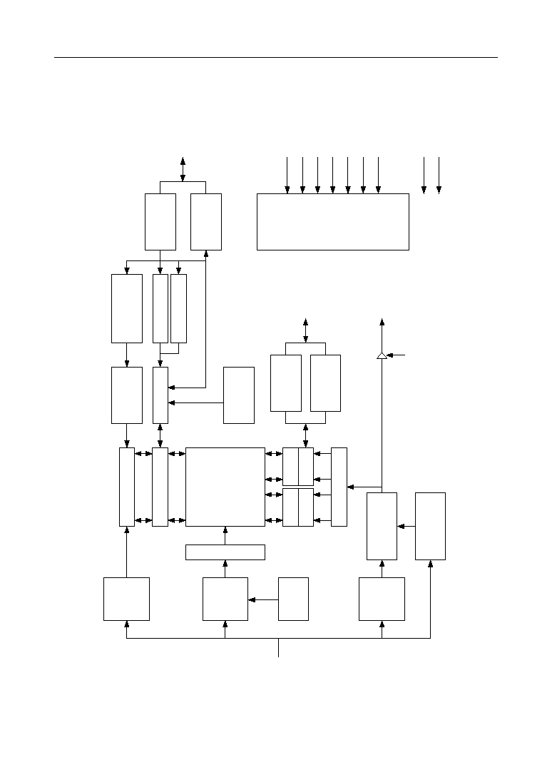
DESCRIPTION
The MSM5416282 is a 4-Mbit CMOS multiport DRAM composed of a 262,144-word by 16-bit
dynamic RAM, and a 512-word by 16-bit SAM. Its RAM and SAM operate independently and
asynchronously.
It supports three types of operations: random access to RAM port, high speed serial access to
SAM port, and bidirectional transfer of data between any selected row in the RAM port and the
SAM port. In addition to the conventional multiport DRAM operating modes, the MSM5416282
features block write and flash write functions on the RAM port, and a split data transfer
capability on the SAM port. The SAM port requires no refresh operation because it uses static
CMOS flip-flops.
FEATURES
∑ Single power supply: 5 V
±
10%
∑ Full TTL compatibility
∑ Multiport organization
RAM : 256K word • 16 bits
SAM : 512 word • 16 bits
∑ Fast page mode
∑ Write per bit
∑ Byte write
∑ Masked flash write
∑ Masked block write (8 columns)
∑ Package:
64-pin 525 mil plastic SSOP
(SSOP64-P-525-0.80-K)
(Product : MSM5416282-xxGS-K)
xx indicates speed rank.
PRODUCT FAMILY
∑ RAS only refresh
∑ CAS before RAS refresh
∑ Hidden refresh
∑ Serial read/write
∑ 512 tap location
∑ Bidirectional data transfer
∑ Split transfer
∑ Masked write transfer
∑ Refresh: 512 cycles/8 ms
Preliminary
Access Time
Cycle Time
Power Dissipation
RAM
RAM
Operating
Standby
SAM
SAM
50 ns
110 ns
180 mA
8 mA
17 ns
20 ns
60 ns
120 ns
170 mA
8 mA
18 ns
22 ns
70 ns
140 ns
160 mA
8 mA
20 ns
22 ns
Family
MSM5416282-50
MSM5416282-60
MSM5416282-70
E2L0022-17-Y1
This version: Jan. 1998
Previous version: Dec. 1996
° Semiconductor
MSM5416282
2/37
PIN CONFIGURATION (TOP VIEW)
Pin Name
Function
A0 - A8
Address Input
RAS
Row Address Strobe
CAS
Column Address Strobe
TRG
Transfer/Output Enable
WEL
Write Enable Lower
Pin Name
Function
SC
Serial Clock
SE
SAM Port Enable
DSF
Special Function Input
V
CC
Power Supply (5 V)
NC
No Connection
DQ0 - DQ15
RAM Inputs/Outputs
SDQ0 - SDQ15
SAM Inputs/Outputs
QSF
Special Function Output
V
SS
Ground (0 V)
WEU
Write Enable Upper
DQ15
SDQ15
DQ14
SDQ14
V
CC
DQ13
SDQ13
DQ12
SDQ12
V
SS
DQ11
SDQ11
DQ10
SDQ10
V
CC
DQ9
SDQ9
SDQ7
DQ7
SDQ6
DQ6
V
SS
SDQ5
DQ5
SDQ4
DQ4
V
SS
SDQ0
DQ0
SDQ1
DQ1
V
CC
SDQ2
DQ2
V
CC
SC
V
SS
V
CC
SDQ3
DQ3
V
SS
SE
TRG
A5
A4
V
CC
DQ8
V
SS
DSF
NC
CAS
QSF
A0
A1
A2
A3
V
SS
SDQ8
WEL
WEU
A6
A7
A8
RAS
1
64-Pin Plastic SSOP
2
3
4
5
6
7
8
9
10
11
13
14
15
16
17
18
19
20
12
21
22
23
24
25
26
27
28
29
30
31
32
64
63
62
61
60
59
58
57
56
55
54
53
52
51
50
49
48
47
46
45
44
43
42
41
40
39
38
37
36
35
34
33
Note:
The same power supply voltage must be provided to every V
CC
pin, and the same GND
voltage level must be provided to every V
SS
pin.
° Semiconductor
MSM5416282
4/37
ELECTRICAL CHARACTERISTICS
Absolute Maximum Ratings
Parameter
Symbol
Rating
Unit
Input Output Voltage
V
T
≠1.0 to 7.0
V
Output Current
I
OS
50
mA
Power Dissipation
P
D
1
W
Operating Temperature
T
opr
0 to 70
∞C
Storage Temperature
T
stg
≠55 to 150
∞C
Condition
Ta = 25∞C
Ta = 25∞C
Ta = 25∞C
--
--
(Note: 1)
Recommended Operating Conditions
Parameter
Symbol
Unit
Power Supply Voltage
V
CC
V
Input High Voltage
V
IH
V
Input Low Voltage
V
IL
V
Min.
4.5
2.4
≠1.0
Typ.
5.0
--
--
Max.
5.5
6.5
0.8
(Ta = 0∞C to 70∞C) (Note: 2)
Capacitance
Parameter
Symbol
Min.
Unit
Input Capacitance
C
i
--
pF
Input/Output Capacitance
C
io
--
pF
Max.
6
7
Output Capacitance
C
o
(QSF)
--
pF
7
(V
CC
= 5 V ±10%, f = 1 MHz, Ta = 25∞C)
Note:
This parameter is periodically sampled and is not 100% tested.
DC Characteristics 1
Parameter
Symbol
Condition
Output "H" Level Voltage
V
OH
I
OH
= ≠2 mA
Output "L" Level Voltage
V
OL
I
OL
= 2 mA
Input Leakage Current
I
LI
0 £ V
IN
£ V
CC
All other pins not
under test = 0 V
Min.
2.4
--
≠10
Max.
--
0.4
10
Unit
V
mA
Output Leakage Current
I
LO
0 £ V
OUT
£ 5.5 V
Output Disable
≠10
10
° Semiconductor
MSM5416282
5/37
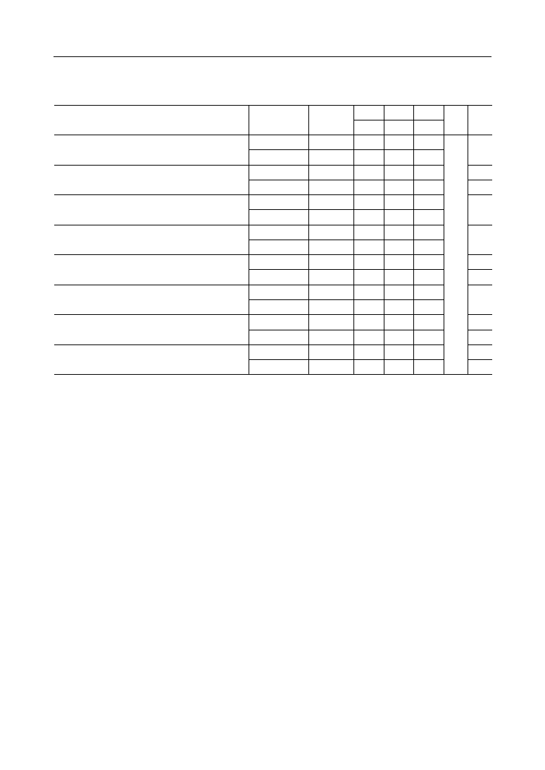
DC Characteristics 2
-50
-60
-70
Unit Note
Symbol
Item (RAM)
SAM
Max. Max. Max.
Operating Current
Standby
(RAS, CAS Cycling, t
RC
= t
RC
min.)
Active
Standby Current
(RAS, CAS = V
IH
)
RAS Only Refresh Current
(RAS Cycling, CAS = V
IH
, t
RC
= t
RC
min.)
Page Mode Current
(RAS = V
IL
, CAS Cycling, t
PC
= t
PC
min.)
CAS before RAS Refresh Current
(RAS Cycling, CAS before RAS, t
RC
= t
RC
min.)
Data Transfer Current
(RAS, CAS Cycling, t
RC
= t
RC
min.)
Flash Write Current
(RAS, CAS Cycling, t
RC
= t
RC
min.)
Block Write Current
(RAS, CAS Cycling, t
RC
= t
RC
min.)
Standby
Active
Standby
Active
Standby
Active
Standby
Active
Standby
Active
Standby
Active
Standby
Active
(V
CC
= 5 V ±10%, Ta = 0∞C to 70∞C)
140
130
120
mA
3, 4
I
CC1
180
170
160
17
8
8
8
60
55
55
3, 4
140
130
120
3, 4
180
170
160
17
150
140
130
3, 4
200
190
180
18
120
110
100
3, 4
160
150
140
3, 4
130
120
110
3, 4
170
160
150
17
130
120
110
3, 4
170
160
150
3, 4
130
120
110
3, 4
170
160
150
3, 4
I
CC1
A
I
CC2
I
CC2
A
I
CC3
I
CC3
A
I
CC4
I
CC4
A
I
CC5
I
CC5
A
I
CC6
I
CC6
A
I
CC7
I
CC7
A
I
CC8
I
CC8
A