1/24
° Semiconductor
MSM5432126/8
DESCRIPTION
The MSM5432126/8 is a new generation Graphics DRAM organized in a 131,072-word • 32-bit
configuration. The technology used to fabricate the MSM5432126/8 is OKI's CMOS silicon gate
process technology. The device operates with a single 5 V power supply.
FEATURES
∑ 131,072-word • 32-bit organization
∑ Single 5 V power supply,
±
10% tolerance
∑ Refresh: 512 cycles/8 ms
∑ Fast Page Mode with Extended Data Out (EDO)
∑ Write per bit (MSM5432128 only)
∑ Byte write, Byte read
∑ RAS only refresh
∑ CAS before RAS refresh
∑ Hidden refresh
∑ Package:
64-pin 525 mil plastic SSOP
(SSOP64-P-525-0.80-K)
(Product : MSM5432126-xxGS-K)
(Product : MSM5432128-xxGS-K)
xx indicates speed rank.
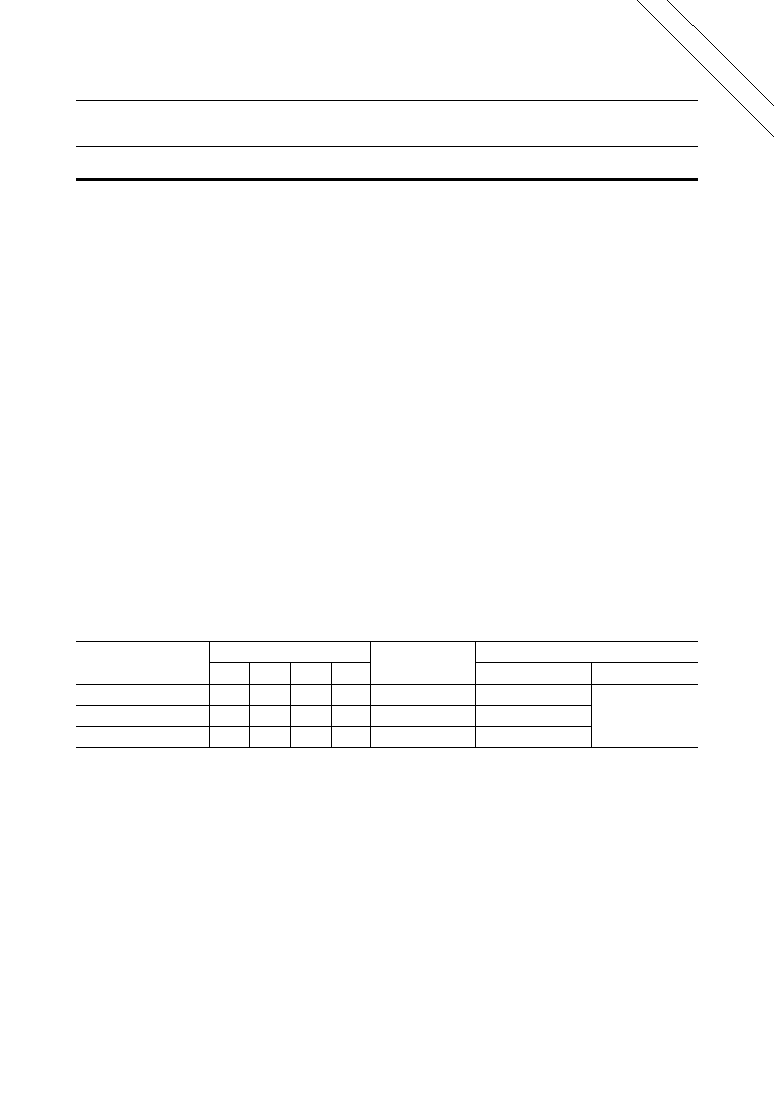
PRODUCT FAMILY
° Semiconductor
MSM5432126/8
131,072-Word
• 32-Bit DYNAMIC RAM : FAST PAGE MODE TYPE WITH EDO
Preliminary
Family
t
RAC
50 ns
60 ns
Operating (Max.)
907 mW
880 mW
Power Dissipation
Cycle Time
(Min.)
110 ns
130 ns
MSM5432126/8-50
MSM5432126/8-60
t
AA
25 ns
30 ns
t
CAC
15 ns
18 ns
Standby (Max.)
Access Time (Max.)
11 mW
t
OEA
15 ns
18 ns
45 ns
935 mW
100 ns
MSM5432126/8-45
23 ns 13 ns 13 ns
This version: Jan. 1998
Previous version: Dec. 1996
E2L0045-17-Y1
2/24
° Semiconductor
MSM5432126/8
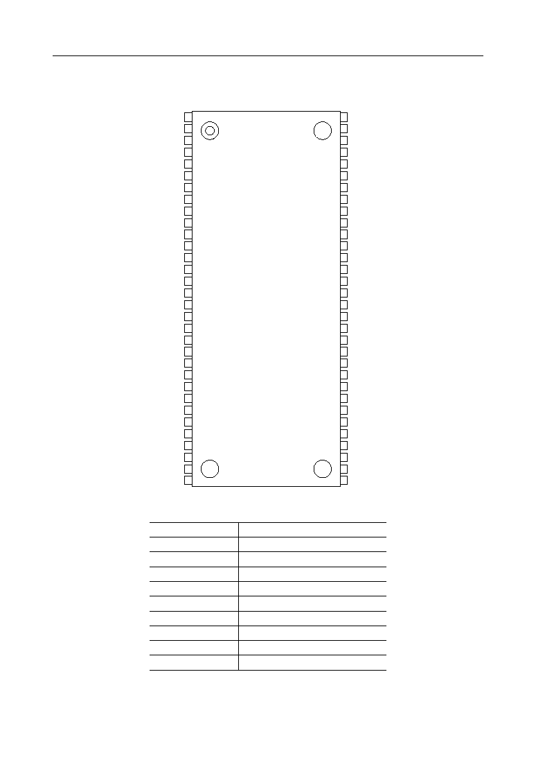
PIN CONFIGURATION (TOP VIEW)
Pin Name
Function
A0 - A8
Address Input
Power Supply (5 V)
Ground (0 V)
NC
No Connection
V
CC
V
SS
DQ0 - DQ31
Data Input / Data Output
RAS
Row Address Strobe
CAS1 - CAS4
Column Address Strobe
Write Per Bit
* / Write Enable
WB* / WE
OE
Output Enable
Note:
The same power supply voltage must be provided to every V
CC
pin, and the same GND
voltage level must be provided to every V
SS
pin.
*:
MSM5432128 only
1
V
CC
64-Pin Plastic SSOP
V
SS
2
DQ0
DQ31
3
DQ1
DQ30
4
DQ2
DQ29
5
DQ3
DQ28
6
V
CC
V
CC
7
DQ4
DQ27
8
DQ5
DQ26
9
DQ6
DQ25
10
DQ7
DQ24
11
V
SS
V
SS
DQ8
DQ23
13
DQ9
DQ22
14
DQ10
DQ21
15
DQ11
DQ20
16
V
CC
V
CC
17
DQ12
DQ19
18
DQ13
DQ18
19
DQ14
DQ17
20
DQ15
DQ16
V
SS
V
SS
NC
CAS1
NC
CAS2
NC
CAS3
WB* / WE
CAS4
RAS
OE
NC
A8
A0
A7
A1
A6
A2
A5
A3
A4
V
CC
V
SS
12
21
22
23
24
25
26
27
28
29
30
31
32
64
63
62
61
60
59
58
57
56
55
54
53
52
51
50
49
48
47
46
45
44
43
42
41
40
39
38
37
36
35
34
33
3/24
° Semiconductor
MSM5432126/8
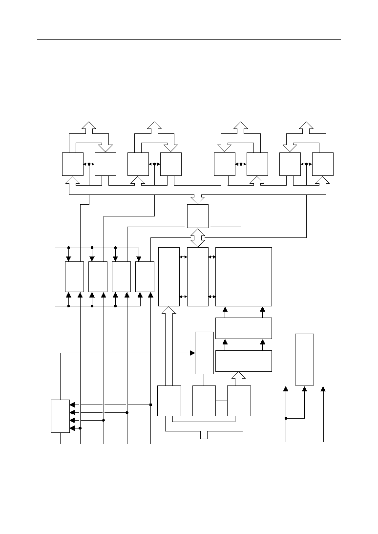
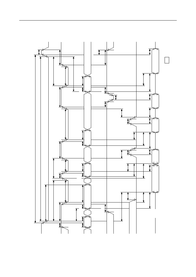
BLOCK DIAGRAM
RAS
CAS4
CAS3
A0 - A8
WB / WE
OE
DQ8 - DQ15
DQ16 - DQ23
V
CC
V
SS
DQ0 - DQ7
DQ24 - DQ31
CAS2
CAS1
Timing
Generator
Refresh
Control Clock
Column
Address
Buffers
Internal
Address
Counter
Row
Address
Buffers
Row
Deco-
ders
Word
Drivers
Memory
Cells
Sense Amps
Column Decoders
8
8
9
9
I/O
Controller
I/O
Controller
32
I/O
Selector
Input
Buffers
Output
Buffers
Output
Buffers
Input
Buffers
32
8
8
8
8
8
8
8
8
On-chip
V
BB
Generator
Input
Buffers
Output
Buffers
Output
Buffers
Input
Buffers
8
8
8
8
8
8
8
8
I/O
Controller
I/O
Controller
4/24
° Semiconductor
MSM5432126/8
ELECTRICAL CHARACTERISTICS
Absolute Maximum Ratings
Recommended Operating Conditions
Input High Voltage
Power Supply Voltage
Input Low Voltage
V
CC
V
SS
V
IH
V
IL
Max.
5.5
0
V
CC
+ 1.0
0.3
V
V
V
V
Typ.
5.0
0
--
--
Min.
4.5
0
3.0
≠0.3
(Ta = 0∞C to 70∞C)
Parameter
Unit
Symbol
Capacitance
Input Capacitance
C
IN
C
IO
pF
pF
Input / Output Capacitance
Max.
8
9
Typ.
--
--
(V
CC
= 5 V ±10%, Ta = 25∞C, f = 1 MHz)
Parameter
Unit
Symbol
Rating
≠0.5 to 7.0
50
1
0 to 70
≠55 to 150
V
mA
W
∞C
∞C
Voltage on Any Pin Relative to V
SS
Short Circuit Output Current
Power Dissipation
Operating Temperature
Storage Temperature
V
T
I
OS
P
D
T
opr
T
stg
Parameter
Unit
Symbol
5/24
° Semiconductor
MSM5432126/8
DC Characteristics
Average Power
Supply Current
(CAS before RAS Refresh)
RAS = cycling,
CAS before RAS
1, 2, 4
mA
130
140
--
--
I
CC5
Average Power
Supply Current
(Fast Page Mode)
RAS = V
IL
,
CAS cycling,
t
HPC
= Min.
1, 2, 4
160
165
--
--
I
CC4
mA
Input Leakage Current
Output High Voltage
Condition
Note
Average Power
Supply Current
(Operating)
Power Supply
Current (Standby)
Output Low Voltage
Output Leakage Current
Unit
Average Power
Supply Current
(RAS Only Refresh)
Parameter
I
OH
= ≠0.1 mA
I
OL
= 0.1 mA
0 V
<
V
IN
<
V
CC
;
All other pins not
under test = 0 V
0 V
<
V
OUT
<
5.5 V
Output Disable
RAS, CAS cycling,
t
RC
= Min.
RAS V
CC
≠ 0.2 V,
CAS V
CC
≠ 0.2 V
RAS = cycling,
CAS = V
IH
,
t
RC
= Min.
V
V
mA
mA
1, 2, 3
mA
mA
1, 2, 3
mA
Max.
V
CC
0.8
10
10
130
2
130
Min.
2.0
0
≠10
≠10
--
Max.
V
CC
0.8
10
10
140
2
140
Min.
2.0
0
≠10
≠10
--
--
--
--
--
Symbol
V
OH
V
OL
I
LI
I
LO
I
CC1
I
CC2
I
CC3
MSM5432126/8
-60
MSM5432126/8
-50
(V
CC
= 5 V ±10%, Ta = 0∞C to 70∞C)
150
--
170
--
Max.
V
CC
0.8
10
10
150
2
150
Min.
2.0
0
≠10
≠10
--
--
--
MSM5432126/8
-45
Notes:
1. Specified values are obtained with minimum cycle time.
2. I
CC
is dependent on output loading. Specified values are obtained with the output
open.
3. Address can be changed once or less while RAS = V
IL
.
4. Address can be changed once or less while CAS = V
IH
.
6/24
° Semiconductor
MSM5432126/8
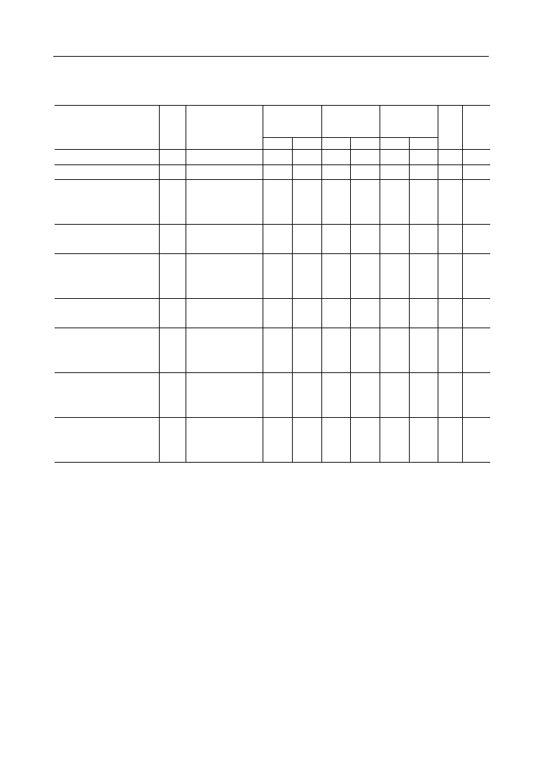
AC Characteristics (1/2)
Parameter
Symbol
Note
Unit
--
t
RC
t
PRWC
t
AA
t
CAC
t
CPA
t
RASP
t
CAS
t
RCD
Max.
Min.
Max.
Min.
MSM5432126/8
-60
MSM5432126/8
-50
--
--
t
HPC
t
RAC
t
REZ
t
RSH
t
CSH
t
T
t
RP
t
RAS
t
RAD
t
ASR
t
RAH
t
ASC
t
CAH
t
AR
t
RCS
t
RCH
t
RRH
t
WCS
t
WCH
--
t
RWC
t
RAL
t
CRP
t
CP
Access Time from Column Address
Column Address Hold Time referenced to RAS
Column Address Set-up Time
Row Address Set-up Time
Access Time from CAS
Column Address Hold Time
CAS Pulse Width
CAS Precharge Time (Hyper Page Mode)
Access Time from CAS Precharge
CAS to RAS Precharge Time
CAS Hold Time
Output Buffer Turn-off Delay Time from RAS
Fast Page Mode Cycle Time
Fast Page Mode Read-Modify-Write Cycle Time
Row Address Hold Time
RAS Pulse Width (Hyper Page Mode Only)
Random Read or Write Cycle Time
RAS to CAS Delay Time
Read Command Hold Time
Read Command Set-up Time
Read Modify Write Cycle
RAS Precharge Time
Read Command Hold Time referenced to RAS
Access Time from RAS
RAS to Column Address Delay Time
Column Address to RAS Lead Time
RAS Pulse Width
RAS Hold Time
Transition Time (Rise and Fall)
Write Command Set-up Time
Write Command Hold Time
ns
--
130
110
ns
30
--
25
--
ns
18
--
15
--
ns
35
--
30
--
ns
35
3
35
3
ns
100k
60
100k
50
ns
--
80
70
ns
10k
9
10k
8
9
20
20
ns
--
24
22
ns
60
--
50
--
5
ns
20
3
20
3
ns
--
64
--
54
ns
--
14
--
14
ns
--
60
--
50
ns
10k
60
10k
50
10
15
15
0
0
9
7
0
0
10
8
40
35
0
0
6, 12
0
0
6
0
0
0
0
10
8
4, 10
4, 9
4, 13
4, 9,10
3
ns
42
35
ns
30
25
ns
ns
ns
ns
ns
ns
ns
ns
ns
ns
ns
--
170
145
ns
--
28
--
24
8
6
9
8
ns
ns
8, 12
--
--
--
--
--
--
--
--
--
--
--
--
--
--
--
--
--
--
--
--
--
--
--
--
t
CEZ
Output Buffer Turn-off Delay Time from CAS
5
ns
20
3
20
3
t
CRL
CAS "H" to RAS "H" Lead Time
0
0
ns
--
--
t
RCL
RAS "H" to CAS "H" Lead Time
0
0
ns
--
--
t
DOH
Data Output Hold after CAS Low
11
3
3
ns
--
--
MSM5432126/8
-45
Max.
--
23
13
28
35
100k
--
10k
--
45
20
--
--
--
10k
32
22
--
--
--
--
--
--
--
--
--
--
--
--
--
--
20
--
--
--
Min.
100
--
--
--
3
45
65
7
20
20
--
3
49
12
45
45
15
0
6
0
7
30
0
0
0
0
7
135
22
6
7
3
0
0
3
(V
CC
= 5 V ±10%, Ta = 0∞C to 70∞C) Note 1, 2, 3
13
15
12
12
12
12
7/24
° Semiconductor
MSM5432126/8
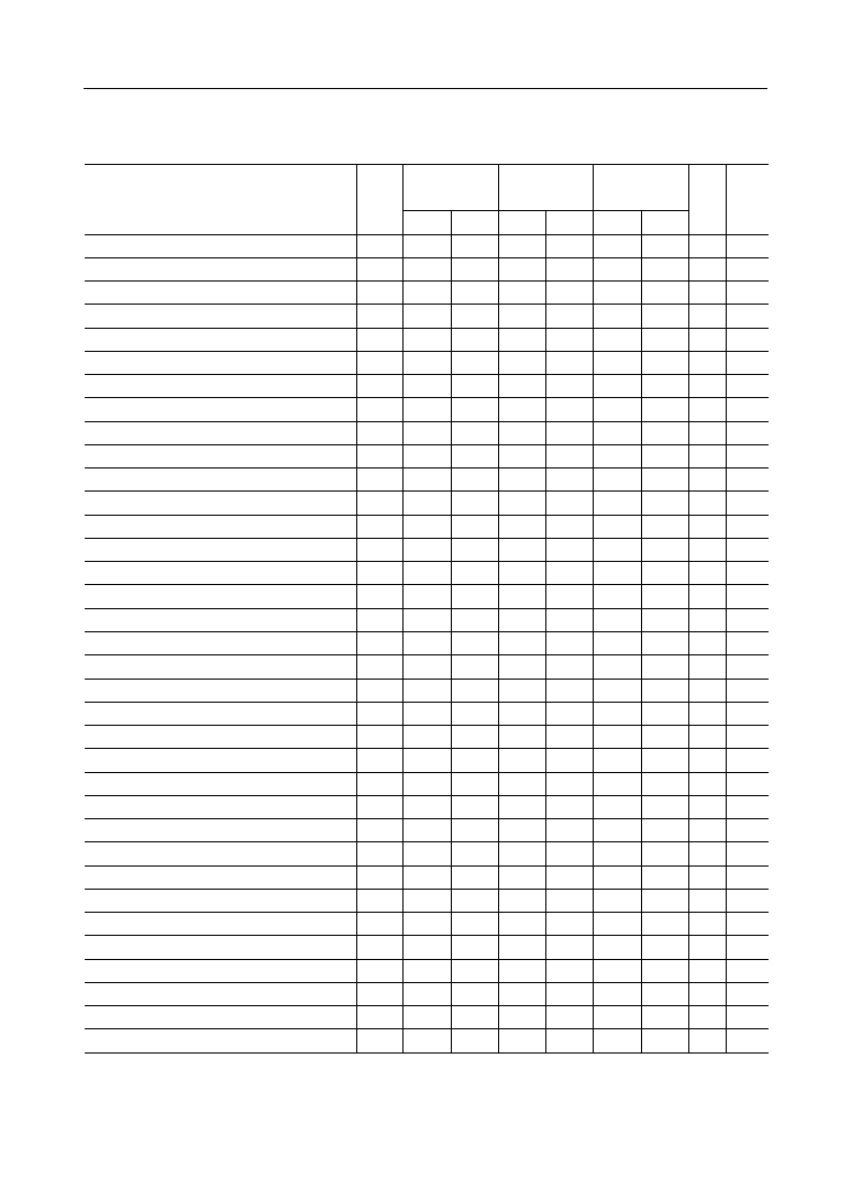
AC Characteristics (2/2)
Parameter
Symbol
Note
Unit
--
t
DS
t
RWD
t
CWD
t
DZC
t
DZO
t
CSR
t
REF
t
WSR
Max.
Min.
Max.
Min.
MSM5432126/8
-60
MSM5432126/8
-50
t
DHR
t
AWD
t
OEA
t
CHR
t
RPC
t
OEZ
t
OEH
t
ROH
t
RWH
t
MS
t
MH
t
DH
Column Address to WE Delay Time
CAS Hold Time for CAS before RAS Cycle
CAS Set-up Time for CAS before RAS Cycle
CAS to WE Delay Time
Data Hold Time
Data Hold Time referenced to RAS
Data Set-up Time
Data to CAS Delay Time
Data to OE Delay Time
Write-Per-Bit Mask Data Hold Time
Write-Per-Bit Mask Data Set-up Time
OE Command Hold Time
Refresh Period
RAS Hold Time referenced to OE
RAS Precharge to CAS Active Time
RAS to WE Delay Time
WB Hold Time
Access Time from OE
WB Set-up Time
Output Buffer Turn-off Delay Time from OE
ns
--
0
0
ns
40
35
ns
0
0
ns
0
0
ns
20
3
20
3
ns
10
8
ns
80
70
ms
8
8
0
0
ns
40
35
ns
50
45
ns
18
15
ns
10
9
ns
10
8
ns
10
10
ns
12
10
8
7
0
0
10
8
8
8
ns
ns
ns
ns
ns
10
8
7, 12
7, 12
8
--
--
--
--
--
--
--
--
--
--
--
--
--
--
--
--
--
--
--
--
--
--
--
--
--
--
--
--
--
--
--
--
--
--
--
--
t
WCR
t
WP
t
RWL
t
CWL
Write Command to CAS Lead Time
Write Command to RAS Lead Time
Write Command Hold Time referenced to RAS
Write Command Pulse Width
40
35
10
9
10
9
10
9
ns
ns
ns
ns
--
--
--
--
--
--
--
--
t
WEZ
Output Buffer Turn-off Delay Time from WE
3
3
ns
20
20
5
5
t
OCH
OE "L" to CAS "H" Lead Time
ns
10
10
--
--
t
CHO
CAS "H" to OE "L" Lead Time
ns
10
10
--
--
t
OEP
High-Z Command Pulse Width
ns
12
10
--
--
t
OED
OE to Data-in Delay Time
ns
12
12
--
--
16
16
16
16
t
CPT
CAS Precharge Time (Refresh Counter Test)
ns
30
25
--
--
MSM5432126/8
-45
--
Max.
Min.
0
32
0
0
20
3
6
65
8
0
30
42
13
8
6
10
10
6
0
7
7
--
--
--
--
--
--
--
--
--
--
--
--
--
--
--
--
--
--
30
8
8
8
--
--
--
--
3
20
10
--
10
--
10
--
12
--
20
--
t
WPE
WB/WE Pulse Width (Output Disable)
ns
12
10
--
--
10
--
14
15
12
13
12
(V
CC
= 5 V ±10%, Ta = 0∞C to 70∞C) Note 1, 2, 3

8/24
° Semiconductor
MSM5432126/8
Notes:
1. An initial pause of 200 ms is required after power-up followed by any 8 RAS cycles
(Example : RAS only refresh) before proper device operation is achieved. In case of
using internal refresh counter, a minimum of 8 CAS before RAS cycles instead of 8 RAS
cycles are required.
2. The AC characteristics assume at t
T
= 3 ns.
3. V
IH
(Min.) and V
IL
(Max.) are reference levels for measuring timing of input signals.
Also, transition times are measured between V
IH
and V
IL
. Input levels at the AC testing
are 3.0 V/0 V.
4. Data outputs are measured with a load of 30 pF.
DOUT reference levels : V
OH
/V
OL
= 2.0 V/0.8 V.
5. t
REZ
(Max.), t
CEZ
(Max.), t
WEZ
(Max.) and t
OEZ
(Max.) define the time at which the
outputs achieve the open circuit condition and are not referenced to output voltage
levels. This parameter is sampled and not 100% tested.
6. Either t
RCH
or t
RRH
must be satisfied for a read cycle.
7. These parameters are referenced to CAS leading edge of early write cycles and to WE
leading edge in OE controlled write cycles and read modify write cycles.
8. t
WCS
, t
RWD
, t
CWD
and t
AWD
are not restrictive operating parameters. They are included
in the data sheet as electrical characteristics only. If t
WCS
t
WCS
(Min.), the cycle is an
early write cycle and the data out pin will remain open circuit throughout the entire
cycle; If t
RWD
t
RWD
(Min.), t
CWD
t
CWD
(Min.) and t
AWD
t
AWD
(Min.), the cycle is
a read modify write cycle and the data out will contain data read from the selected cell:
If neither of the above sets of conditions is satisfied, the condition of the data out is
indeterminate.
9. Operation within the t
RCD
(Max.) limit ensures that t
RAC
(Max.) can be met.
t
RCD
(Max.) is specified as a reference point only: If t
RCD
is greater than the specified
t
RCD
(Max.) limit, then access time is controlled by t
CAC
.
10. Operation within the t
RAD
(Max.) limit ensures that t
RAC
(Max.) can be met. t
RAD
(Max.)
is specified as a reference point only: If t
RAD
is greater than the specified t
RAD
(Max.)
limit, then access time is controlled by t
AA
.
11. This is guaranteed by design. (t
DOH
= t
CAC
- output transition time) This parameter is
not 100% tested.
12. These parameters are determined by the earliest falling edge of CAS1, CAS2, CAS3, or
CAS4.
13. These parameters are determined by the latest rising edge of CAS1, CAS2, CAS3, or
CAS4.
14. t
CWL
should be satisfied by all CASes.
15. t
CP
and t
CPT
are determined by the time that all CASes are high.
16. Only MSM5432128.
9/24
° Semiconductor
MSM5432126/8
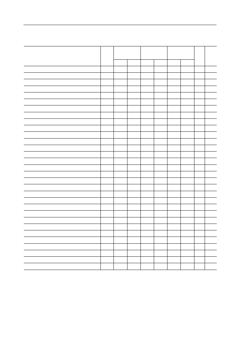
CASn-DQ FUNCTION TABLE
CAS1
H
H
CAS2
H
H
CAS3
H
H
CAS4
H
L
DQ0-7
*
*
DQ8-15
*
*
DQ16-23
*
*
DQ24-31
*
Enable
H
H
L
H
*
*
Enable
*
H
H
L
L
*
*
Enable
Enable
H
L
H
H
*
Enable
*
*
H
L
H
L
*
Enable
*
Enable
H
L
L
H
*
Enable
Enable
*
H
L
L
L
*
Enable
Enable
Enable
L
H
H
H
Enable
*
*
*
L
H
H
L
Enable
*
*
Enable
L
H
L
H
Enable
*
Enable
*
L
H
L
L
Enable
*
Enable
Enable
L
L
H
H
Enable
Enable
*
*
L
L
H
L
Enable
Enable
*
Enable
L
L
L
H
Enable
Enable
Enable
*
L
L
L
L
Enable
Enable
Enable
Enable
Read cycle
Write cycle
Enable
Valid Data-out
Write Data
*
High-Z
Don't Care
WRITE CYCLE FUNCTION TABLE
A
B
RAS falling edge
CODE
CAS or WB / WE falling edge
Function
C
WB / WE
DQ
DQ
L
Write mask
Write data
H (*2)
Don't care
Write data
RWM (*1)
Write per bit
RW
Normal write
Write mask : 'L' = Mask, 'H' = No mask
(*1):
MSM5432128 only.
(*2):
In case of MSM5432126, don't care.
10/24
° Semiconductor
MSM5432126/8
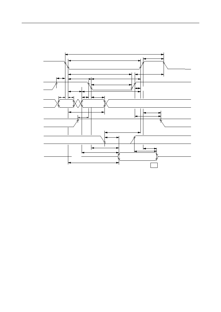
TIMING WAVEFORM
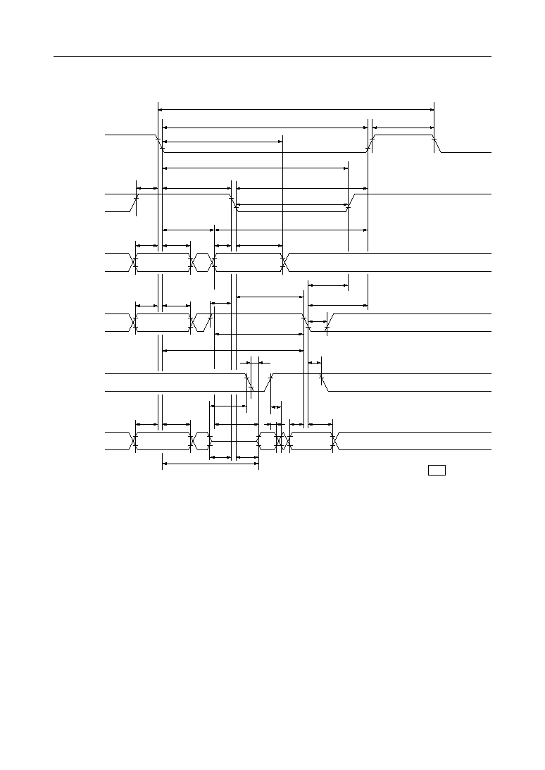
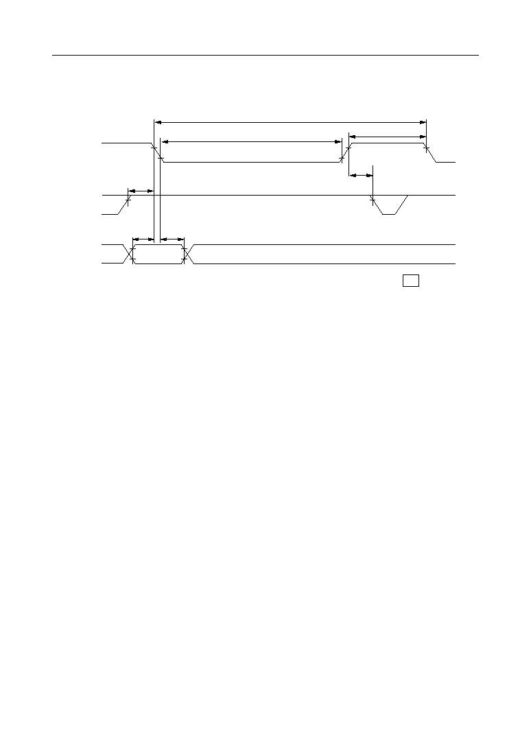
Read Cycle (Outputs Controlled by RAS)
,
,,
RAS
Address
WB / WE
DQ0 - DQ31
CAS1
|
CAS4
,
"H" or "L"
OE
t
RC
t
RAS
t
RP
t
CRP
t
CSH
t
CRP
t
RCD
t
RSH
t
CAS
t
RAD
t
ASR
t
RAH
t
ASC
t
CAH
t
RAL
Row
Column
t
RCS
t
RRH
t
RCH
t
ROH
t
OEA
t
CAC
t
AA
t
OEZ
t
REZ
Open
Valid Data-out
t
CRL
t
AR
t
RAC
11/24
° Semiconductor
MSM5432126/8
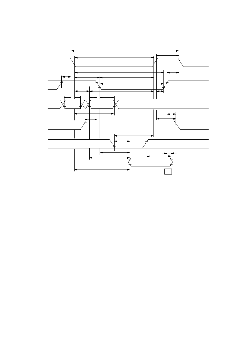
Read Cycle (Outputs Controlled by CAS)
,
,,
RAS
Address
WB / WE
DQ0 - DQ31
CAS1
|
CAS4
,
"H" or "L"
OE
t
RC
t
RAS
t
RP
t
AR
t
CRP
t
CSH
t
CRP
t
RCD
t
RSH
t
CAS
t
RAD
t
ASR
t
RAH
t
ASC
t
CAH
t
RAL
Row
Column
t
RCS
t
RRH
t
RCH
t
AA
t
ROH
t
OEA
t
CAC
t
OEZ
t
CEZ
Open
Valid Data-out
t
RCL
t
RAC
12/24
° Semiconductor
MSM5432126/8
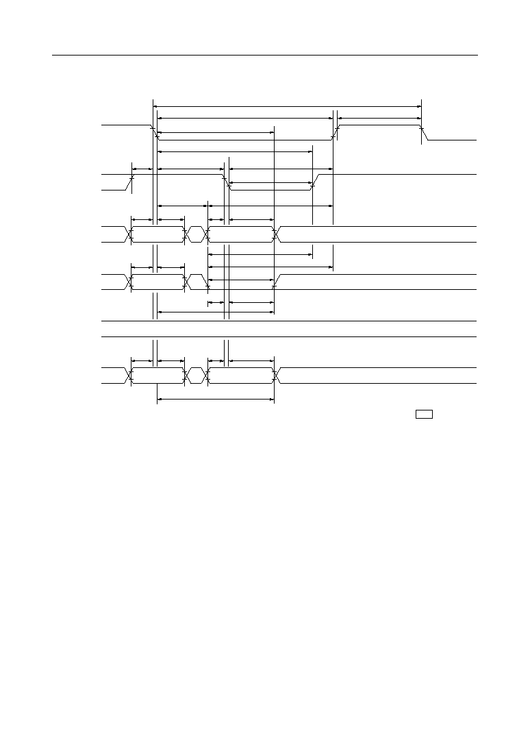
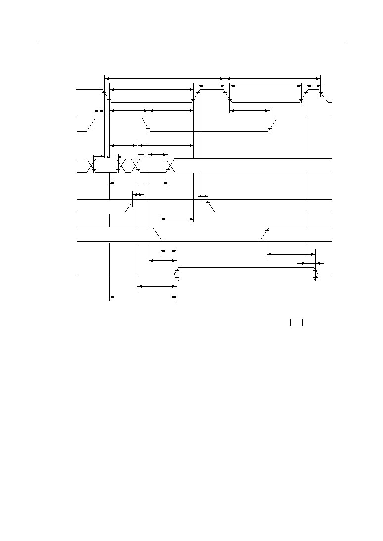
Write Cycle (Early Write)
RAS
CAS1
|
CAS4
Address
t
RC
t
RAS
t
RP
t
RCD
t
CAS
t
RSH
t
CSH
t
CRP
t
AR
t
RAD
t
RAL
Row
Column
t
RAH
t
ASC
t
CAH
t
ASR
"H" or "L"
WB / WE
A
t
RWH
t
WP
t
WSR
DQ0 - DQ31
,
,,
B
C
t
MH
t
DS
t
DH
t
MS
OE
,,,,
t
RWL
t
CWL
t
DHR
t
WCH
t
WCR
t
WCS
13/24
° Semiconductor
MSM5432126/8
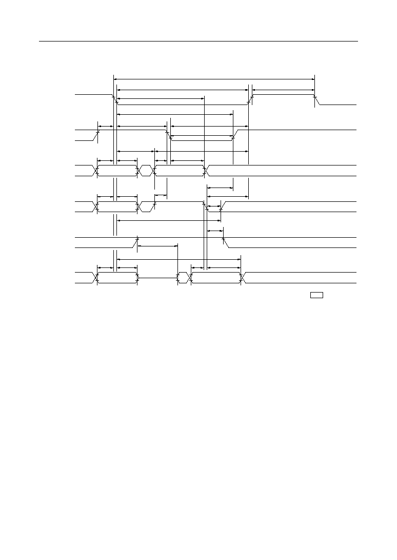
Write Cycle (OE Control Write)
RAS
CAS1
|
CAS4
Address
t
RC
t
RAS
t
RP
t
RCD
t
CAS
t
RSH
t
CSH
t
CRP
t
AR
t
RAD
t
RAL
Row
Column
t
RAH
t
ASC
t
CAH
t
ASR
"H" or "L"
WB / WE
A
t
RWH
t
WSR
DQ0 - DQ31
B
C
t
MH
t
DS
t
DH
t
MS
OE
,
,,,
t
RWL
t
CWL
t
DHR
t
WCR
t
WP
t
OEH
,,
t
OED
t
RCS
14/24
° Semiconductor
MSM5432126/8
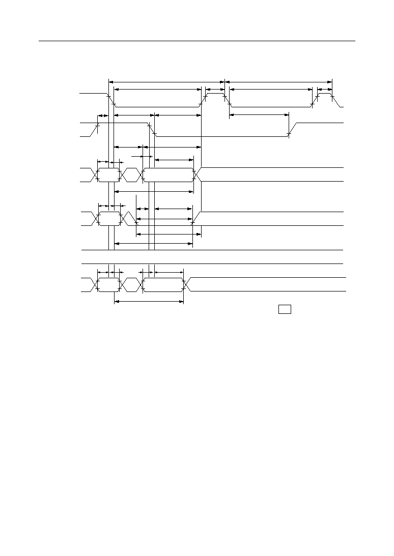
Read Modify Write Cycle
RAS
CAS1
|
CAS4
Address
t
RWC
t
RAS
t
RP
t
RCD
t
CAS
t
RSH
t
CSH
t
CRP
t
AR
t
RAD
t
RAL
Row
Column
t
RAH
t
ASC
t
CAH
t
ASR
"H" or "L"
WB / WE
,
A
t
RWH
t
WSR
DQ0 - DQ31
B
C
t
AA
t
DS
t
DH
t
MS
OE
,,
t
RWL
t
CWL
t
RWD
t
WP
t
OEH
t
AWD
t
OEA
t
RAC
t
CAC
t
MH
t
OED
t
OEZ
t
RCS
OUT
t
DZC
t
DZO
t
CWD
15/24
° Semiconductor
MSM5432126/8
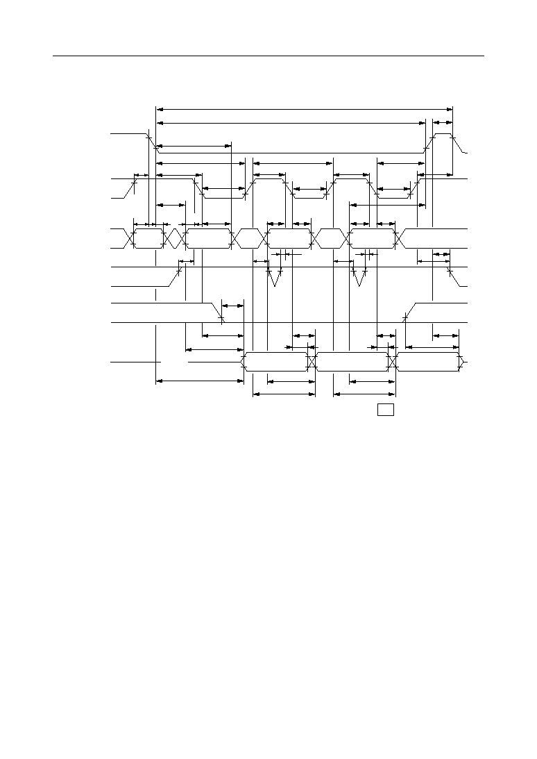
Fast Page Mode Read Cycle with EDO
RAS
Address
WB / WE
DQ0 - DQ31
CAS1
|
CAS4
OE
,
,
Row
Column
t
CRP
t
RP
t
RASP
t
CAS
"H" or "L"
,
Column
,
Column
t
RCD
t
CP
t
CAS
t
CAS
t
HPC
t
CAH
t
ASC
t
RAD
t
RCS
t
RRH
t
AR
t
AA
Valid
Data-out
t
RAH
t
ASR
t
CAH
t
ASC
t
CAH
t
ASC
t
RC
t
CSH
t
CRP
t
CP
t
RSH
t
RAL
t
RCH
t
RCS
t
RCH
t
RCS
t
RCH
t
CAC
Open
t
RAC
Valid
Data-out
Valid
Data-out
t
OEA
t
CAC
t
CAC
t
REZ
t
DOH
t
DOH
t
OEZ
t
AA
t
AA
t
CPA
t
CPA
16/24
° Semiconductor
MSM5432126/8
Fast Page Mode Write Cycle (Early Write)
RAS
Address
WB / WE
DQ0 - DQ31
CAS1
|
CAS4
OE
"H" or "L"
t
ASR
Row
Column
Column
Column
A
,
B
t
RAH
t
ASC
t
RAD
t
CAH
t
ASC
t
CAH
t
CAH
t
ASC
t
CRP
t
RCD
t
CAS
t
AR
t
RP
t
RASP
t
RC
t
CSH
t
HPC
t
RSH
t
CRP
t
CAS
t
CAS
t
CP
t
RAL
t
WSR
t
RWH
t
CWL
t
WCS
t
WP
t
WCH
t
CWL
t
WCS
t
WP
t
WCH
t
CWL
t
WCS
t
WP
t
WCH
t
RWL
t
WCR
t
MS
t
MH
C
t
DS
t
DH
C
t
DS
t
DH
C
t
DS
t
DH
,
,
,
t
CP
t
DHR
17/24
° Semiconductor
MSM5432126/8
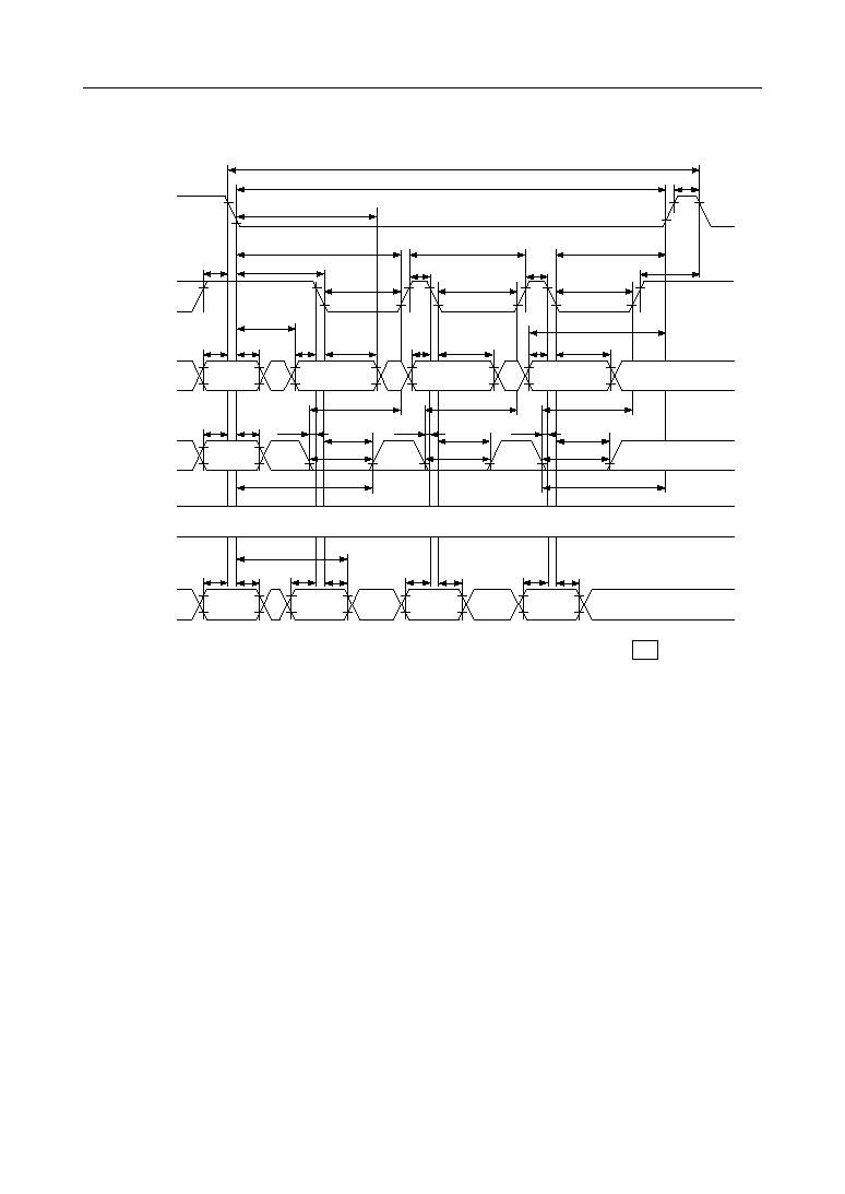
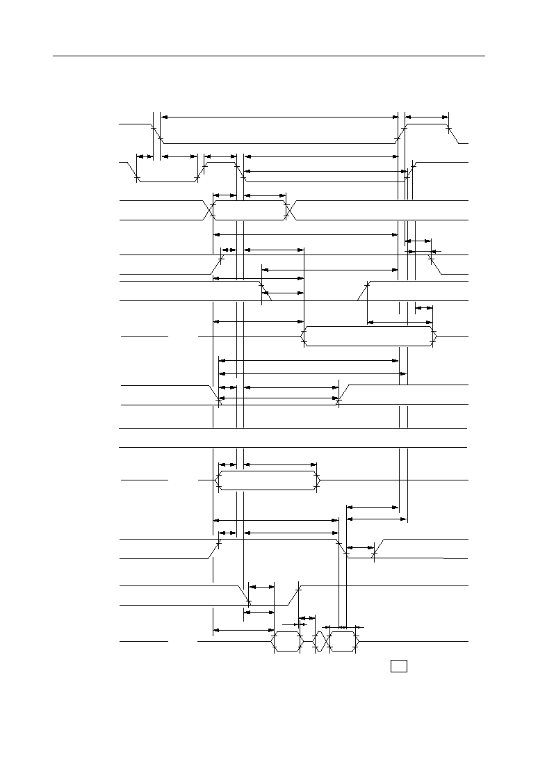
Fast Page Mode Read Modify Write Cycle
RAS
Address
WB / WE
DQ0 - DQ31
CAS1
|
CAS4
OE
"H" or "L"
t
ASR
Row
Column
Column
Column
A
,
B
t
RAH
t
ASC
t
RAD
t
CAH
t
ASC
t
CAH
t
CAH
t
ASC
t
CRP
t
RCD
t
CAS
t
AR
t
RP
t
RASP
t
RC
t
CSH
t
PRWC
t
RSH
t
CRP
t
CAS
t
CAS
t
CP
t
RAL
t
WSR
t
RWH
t
CWD
t
RCS
t
CWD
t
RWD
t
MS
t
MH
t
CP
t
AWD
t
WP
t
CWL
t
AWD
t
CWL
t
WP
t
CWD
t
RWL
t
CWL
t
WP
t
OEA
,,
t
OEA
t
AWD
t
OEA
,
t
OEH
,
t
AA
t
OEZ
t
OED
OUT
t
RAC
t
CAC
t
DH
t
DS
t
AA
t
OEZ
t
OED
OUT
t
DH
t
DS
t
CAC
OUT
t
CAC
t
AA
t
DS
t
DH
t
OEZ
t
OED
C
C
C
t
ROH
18/24
° Semiconductor
MSM5432126/8
RAS Only Refresh Cycle
RAS
Address
CAS1
|
CAS4
t
CRP
t
RP
t
RAS
t
RPC
,
,,,
Row
t
ASR
t
RAH
t
RC
"H" or "L"
Note: DQs are open, WB / WE, OE = "H" or "L"

19/24
° Semiconductor
MSM5432126/8
CAS before RAS Refresh Cycle
RAS
CASn
t
RP
t
RAS
Open
t
RC
t
RPC
t
CP
t
CSR
t
CHR
t
CEZ
t
RP
DQ0 - DQ31
Note: WB / WE, OE, A0 - A8 = "H" or "L"
20/24
° Semiconductor
MSM5432126/8
Hidden Refresh Read Cycle
RAS
CAS1
|
CAS4
Address
OE
"H" or "L"
,
WB / WE
DQ0 - DQ31
,
,,
t
RC
t
RC
t
RAS
t
RP
t
RAS
t
RP
t
AR
t
CRP
t
RCD
t
RSH
t
CHR
t
RAD
t
ASR
t
RAH
t
ASC
t
CAH
Row
Column
t
RCS
t
RAL
t
RRH
t
AA
t
ROH
t
OEA
t
CAC
t
RAC
t
OEZ
Valid Data-out
t
REZ
21/24
° Semiconductor
MSM5432126/8
Hidden Refresh Write Cycle
RAS
Address
WB / WE
DQ0 - DQ31
CAS1
|
CAS4
OE
"H" or "L"
t
ASR
Row
Column
t
CRP
t
RC
t
ASC
t
RP
t
RAS
t
RCD
t
RSH
t
RAD
t
CAH
t
RAH
t
RAL
t
RWL
t
CHR
t
RAS
t
RC
t
RP
t
AR
,,,
t
WP
t
WCH
,,
t
WCR
t
WCS
,
t
WSR
t
RWH
C
A
t
DHR
t
MS
t
MH
t
DH
t
DS
B
22/24
° Semiconductor
MSM5432126/8
RAS
Address
WB / WE
DQ0 - DQ31
CAS1
|
CAS4
OE
t
RAS
t
ASC
t
CPT
t
RSH
t
CAH
t
CAS
"H" or "L"
,,,
t
WP
t
CWL
t
RP
Valid Data-out
Open
t
AA
t
CEZ
t
CAC
,
Open
t
RCS
t
RWL
Valid
Data-out
t
RCS
t
AWD
t
CWD
t
RWL
t
WP
t
CWL
t
CAC
t
OEZ
t
CHR
t
CSR
Column
t
RCH
t
RRH
,
,
t
OEZ
t
OEA
t
ROH
t
WCH
t
WCS
t
DH
Valid
Data-in
,
t
DS
t
DH
t
OED
t
OEA
,
t
DS
Valid Data-in
Read Cycle
Write Cycle
WB / WE
OE
DQ0 - DQ31
Read Modify Write Cycle
WB / WE
OE
DQ0 - DQ31
Open
t
AA
t
AA
t
RAL
CAS before RAS Refresh Counter Test Cycle
23/24
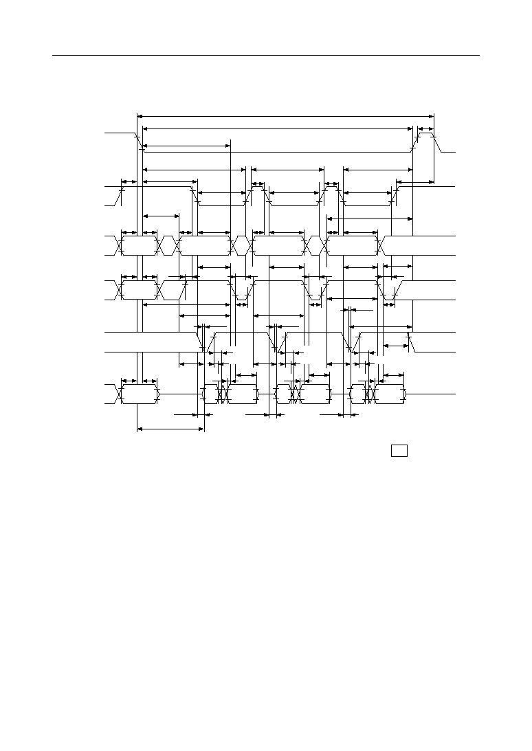
° Semiconductor
MSM5432126/8
"H" or "L"
t
AR
RAS
CAS1
|
CAS4
Address
Row
Column
Column
Column
t
RASP
t
RC
t
RP
t
CRP
t
RCD
t
CSH
t
CAS
t
HPC
t
CP
t
CAS
t
CP
t
CAS
t
CP
t
CAS
t
RSH
t
CRP
t
ASR
t
RAH
t
ASC
t
RAD
t
CAH
t
ASC
t
CAH
t
ASC
t
CAH
Column
t
ASC
t
CAH
t
RAL
WB / WE
t
RCS
t
RRH
t
RCH
t
RCH
t
WPE
OE
,
t
OEA
t
RAC
t
CAC
t
AA
t
CHO
t
OEP
t
OCH
t
OEP
DQ0 - DQ31
t
AA
t
CAC
t
DOH
t
CPA
Valid
Data-out
Valid
Data-out
t
OEZ
t
OEA
Valid*
Data-out
t
AA
t
CAC
t
OEZ
Valid*
Data-out
t
WEZ
t
OEA
t
AA
t
CAC
Valid
Data-out
t
REZ
* : Same Data
Open
t
RCS
Fast Page Mode Read with EDO High-Z Operation
24/24
° Semiconductor
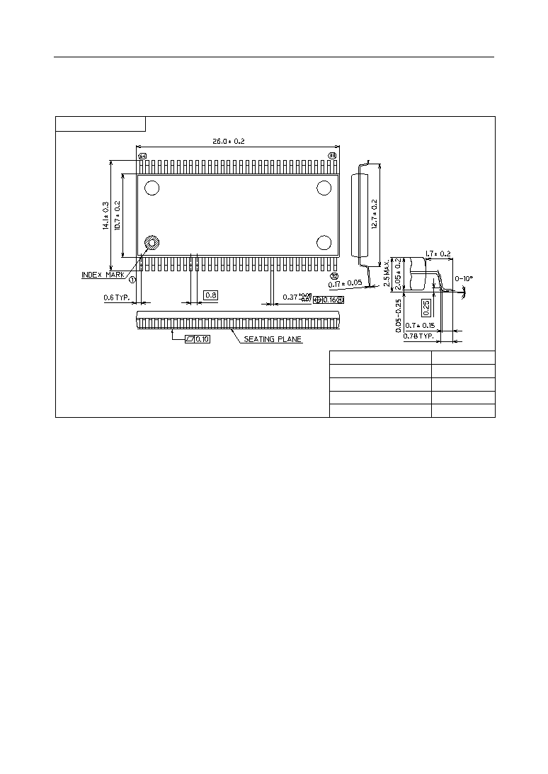
MSM5432126/8
(Unit : mm)
PACKAGE DIMENSIONS
Notes for Mounting the Surface Mount Type Package
The SOP, QFP, TSOP, SOJ, QFJ (PLCC), SHP and BGA are surface mount type packages, which
are very susceptible to heat in reflow mounting and humidity absorbed in storage.
Therefore, before you perform reflow mounting, contact Oki's responsible sales person for the
product name, package name, pin number, package code and desired mounting conditions
(reflow method, temperature and times).
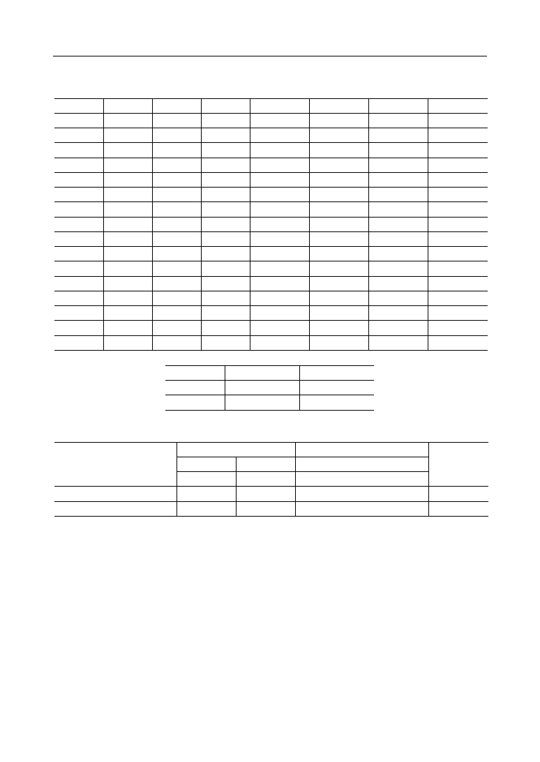
SSOP64-P-525-0.80-K
Package material
Lead frame material
Pin treatment
Solder plate thickness
Package weight (g)
Epoxy resin
42 alloy
Solder plating
5 mm or more
1.34 TYP.
Mirror finish