
MSM54C865
° Semiconductor
1/44
DESCRIPTION
The MSM54C865 is a 512Kbit CMOS multiport DRAM composed of a 65,536-word by 8-bit
dynamic RAM and a 256-word by 8-bit SAM. Its RAM and SAM operate independently and
asynchronously.
The MSM54C865 supports three types of operaton: random access to RAM port, high speed serial
access to SAM port and bidirectional transfer of data between any selected row in the RAM port
and the SAM port. In addition to the conventional multiport DRAM operating modes, the
MSM54C865 features the block write and flash write functions on the RAM port and a split data
transfer capability on the SAM port. The SAM port requires no refresh operation because it uses
static CMOS flip-flops.
FEATURES
∑ Single power supply: 5 V
±
10%
∑ Full TTL compatibility
∑ Multiport organization
RAM : 64K word • 8 bits
SAM : 256 word • 8 bits
∑ Fast page mode
∑ Write per bit
∑ Masked flash write
∑ Masked block write
∑ RAS only refresh
∑ CAS before RAS refresh
∑ Hidden refresh
∑ Serial read/write
∑ 256 tap location
∑ Bidirectional data transfer
∑ Split transfer
∑ Masked write transfer
∑ Refresh :256 cycles/4 ms
∑ Package options:
40-pin 475 mil plastic ZIP
(ZIP40-P-475-1.27)
(Product : MSM54C865-xxZS)
40-pin 400 mil plastic SOJ
(SOJ40-P-400-1.27)
(Product : MSM54C865-xxJS)
xx indicates speed rank.
PRODUCT FAMILY
° Semiconductor
MSM54C865
65,536-Word
• 8-Bit Multiport DRAM
Family
MSM54C865-70
MSM54C865-80
MSM54C865-10
Access Time
RAM
SAM
70 ns
25 ns
80 ns
25 ns
100 ns
25 ns
Cycle Time
RAM
SAM
140 ns
30 ns
150 ns
30 ns
180 ns
30 ns
Power Dissipation
Operating
120 mA
110 mA
100 mA
Standby
8 mA
8 mA
8 mA
E2L0011-17-Y1
This version: Jan. 1998
Previous version: Dec. 1996
MSM54C865
° Semiconductor
2/44
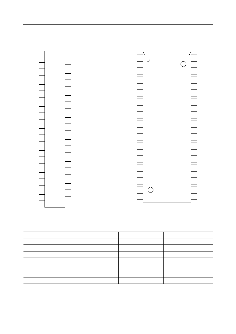
PIN CONFIGURATION (TOP VIEW)
W6/IO6
W8/IO8
SIO5
SIO7
V
SS1
SIO1
SIO3
DT/OE
W2/IO2
V
SS3
V
CC1
RAS
A6
NC
A4
V
CC2
A3
A1
QSF
DSF
SC
SIO1
SIO2
SIO3
SIO4
DT/OE
W1/IO1
W2/IO2
W3/IO3
W4/IO4
V
CC1
WB/WE
NC
RAS
NC
NC
A6
A5
A4
V
CC2
V
SS1
SIO8
SIO7
SIO6
SIO5
SE
W8/IO8
W7/IO7
W6/IO6
W5/IO5
V
SS2
DSF
NC
CAS
QSF
A0
A1
A2
A3
A7
1
2
3
4
5
6
7
8
9
10
11
12
13
14
15
16
17
18
19
20
40
39
38
37
36
35
34
33
32
31
30
29
28
27
26
25
24
23
22
21
2
4
6
8
10
12
14
16
18
20
22
24
26
28
30
32
34
36
38
40
1
3
5
7
9
11
13
15
17
19
21
23
25
27
29
31
33
35
37
39
40-Pin Plastic SOJ
40-Pin Plastic ZIP
W5/IO5
W7/IO7
SE
SIO6
SIO8
SC
SIO2
SIO4
W1/IO1
W3/IO3
W4/IO4
WB/WE
NC
V
SS2
A5
NC
A7
A2
A0
CAS
Pin Name
A0 - A7
W1/IO1 - W8/IO8
SIO1 - SIO8
RAS
CAS
WB/WE
DT/OE
Function
Address Input
RAM Inputs/Outputs
SAM Inputs/Outputs
Row Address Strobe
Column Address Strobe
Write per Bit/Write Enable
Transfer/Output Enable
Pin Name
SC
SE
DSF
QSF
V
CC
V
SS
NC
Function
Serial Clock
SAM Port Enable
Special Function Input
Special Function Output
Power Supply (5 V)
Ground (0 V)
No Connection
Note :
The same power supply voltage must be provided to every V
CC
pin, and the same GND
voltage level must be provided to every V
SS
pin.
MSM54C865
° Semiconductor
3/44
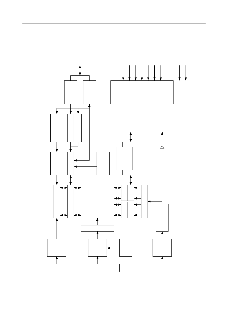
BLOCK DIAGRAM
Column
Address
Buffer
Row
Address
Buffer
Refresh
Counter
A0 - A7
SAM
Address
Buffer
SAM Address
Counter
Row Decoder
Column Decoder
Sense Amp.
256 • 256 • 8
RAM ARRAY
Gate
SAM
Gate
SAM
SIO1
- SIO8
QSF
Serial Decoder
Block Write
Control
I/O Control
Flash Write
Control
SAM Input
Buffer
SAM Output
Buffer
Column Mask
Register
Color Register
Mask Register
RAM Input
Buffer
RAM Output
Buffer
Timing
Generator
RAS
CAS
DT/OE
WB/WE
DSF
SC
SE
V
CC
V
SS
W1/IO1
- W8/IO8
MSM54C865
° Semiconductor
4/44
ELECTRICAL CHARACTERISTICS
Absolute Maximum Ratings
Parameter
Input Output Voltage
Output Current
Power Dissipation
Operating Temperature
Storage Temperature
Symbol
V
T
I
OS
P
D
T
opr
T
stg
Condition
Ta = 25∞C
Ta = 25∞C
Ta = 25∞C
--
--
Rating
≠1.0 to 7.0
50
1
0 to 70
≠55 to 150
Unit
V
mA
W
∞C
∞C
(Note: 16)
Recommended Operating Conditions
Parameter
Power Supply Voltage
Input High Voltage
Input Low Voltage
Symbol
V
CC
V
IH
V
IL
Min.
4.5
2.4
≠1.0
Unit
V
V
V
(Ta = 0∞C to 70∞C) (Note: 17)
Typ.
5.0
--
--
Max.
5.5
6.5
0.8
Capacitance
Parameter
Input Capacitance
Input/Output Capacitance
Output Capacitance
Symbol
C
I
C
I/O
C
O
(QSF)
Min.
--
--
--
Unit
pF
pF
pF
(V
CC
= 5 V ±10%, f = 1 MHz, Ta = 25∞C)
Max.
7
9
9
Note:
This parameter is periodically sampled and is not 100% tested.
DC Characteristics 1
Parameter
Output "H" Level Voltage
Output "L" Level Voltage
Input Leakage Current
Output Leakage Current
Symbol
V
OH
V
OL
I
LI
I
LO
Condition
I
OH
= ≠2 mA
I
OL
= 2 mA
0 £ V
IN
£ V
CC
0 £ V
OUT
£ 5.5 V
Min.
2.4
--
≠10
≠10
Unit
V
mA
All other pins not
Output Disable
Max.
--
0.4
10
10
under test = 0 V

MSM54C865
° Semiconductor
5/44
DC Characteristics 2
-70
-80
-10
Unit Note
Symbol
Item (RAM)
SAM
Max. Max. Max.
85
75
65
mA
1, 2
I
CC1
Operating Current
Standby
120
110
100
1, 2
(RAS, CAS Cycling, t
RC
= t
RC
min.)
Active
8
8
8
Standby Current
50
45
40
1, 2
(RAS, CAS = V
IH
)
85
75
65
1, 2
RAS Only Refresh Current
120
110
100
1, 2
(RAS Cycling, CAS = V
IH
, t
RC
= t
RC
min.)
70
65
60
1, 2
Page Mode Current
120
110
100
1, 2
(RAS = V
IL
, CAS Cycling, t
PC
= t
PC
min.)
85
75
65
1, 2
CAS before RAS Refresh Current
120
110
100
1, 2
(RAS Cycling, CAS before RAS, t
RC
= t
RC
min.)
85
75
65
1, 2
Data Transfer Current
120
110
100
1, 2
(RAS, CAS Cycling, t
RC
= t
RC
min.)
85
75
65
1, 2
Flash Write Current
120
110
100
1, 2
(RAS, CAS Cycling, t
RC
= t
RC
min.)
85
75
65
1, 2
Block Write Current
120
110
100
1, 2
(RAS, CAS Cycling, t
RC
= t
RC
min.)
I
CC1A
I
CC2
I
CC2A
I
CC3
I
CC3A
I
CC4
I
CC4A
I
CC5
I
CC5A
I
CC6
I
CC6A
I
CC7
I
CC7A
I
CC8
I
CC8A
Standby
Active
Standby
Active
Standby
Active
Standby
Active
Standby
Active
Standby
Active
Standby
Active
(V
CC
= 5 V ±10%, Ta = 0∞C to 70∞C)
3

MSM54C865
° Semiconductor
6/44
AC Characteristics (1/3)
Parameter
Symbol
Note
Unit
ns
180
150
--
140
ns
55
40
35
--
ns
25
25
20
--
ns
50
45
40
--
ns
35
3
35
3
35
3
ns
100k
100
100k
80
100k
70
t
RC
t
PRWC
t
AA
t
CAC
t
CPA
t
RASP
t
CAS
t
RCD
Max.
Min.
Max.
Min.
Max.
Min.
-10
-80
-70
ns
100
90
--
90
ns
10k
25
10k
25
10k
20
13
20
20
20
ns
55
50
--
45
t
PC
t
RAC
ns
100
80
70
--
9
ns
20
0
20
0
20
0
t
OFF
ns
--
70
--
60
--
60
ns
--
25
--
25
--
20
t
RSH
ns
--
100
--
80
--
70
t
CSH
t
T
t
RP
ns
10k
100
10k
80
10k
70
t
RAS
t
RAD
13
20
15
15
t
ASR
0
0
0
t
RAH
10
10
10
t
ASC
0
0
0
t
CAH
15
15
15
t
AR
70
55
55
t
RCS
0
0
0
t
RCH
10
0
0
0
t
RRH
10
0
0
0
t
WCH
15
15
15
t
WCR
70
55
55
t
WP
15
15
15
t
RWL
25
20
20
t
CWL
25
20
20
7, 13
7, 14
7, 14
7, 13
6
ns
75
55
50
ns
50
40
35
ns
ns
ns
ns
ns
ns
ns
ns
ns
ns
ns
ns
ns
ns
235
195
--
195
t
RWC
t
RAL
t
CRP
ns
--
55
--
40
--
35
10
10
10
t
CP
10
10
10
ns
ns
--
--
--
--
--
--
--
--
--
--
--
--
--
--
--
--
--
--
--
--
--
--
--
--
--
--
--
--
--
--
--
--
--
--
--
--
--
--
--
--
--
--
--
--
--
--
--
--
--
--
--
--
--
--
--
--
--
--
--
--
--
Access Time from Column Address
Column Address Hold Time referenced to RAS
Column Address Set-up Time
Row Address Set-up Time
Access Time from CAS
Column Address Hold Time
CAS Pulse Width
CAS Precharge Time (Fast Page Mode)
Access Time from CAS Precharge
CAS to RAS Precharge Time
CAS Hold Time
Write Command to CAS Lead Time
Output Buffer Turn-off Delay
Fast Page Mode Cycle Time
Fast Page Mode Read Modify Write Cycle Time
Row Address Hold Time
RAS Pulse Width (Fast Page Mode Only)
Random Read or Write Cycle Time
RAS to CAS Delay Time
Read Command Hold Time
Read Command Set-up Time
Read Modify Write Cycle Time
RAS Precharge Time
Read Command Hold Time referenced to RAS
Write Command to RAS Lead Time
Access Time from RAS
RAS to Column Address Delay Time
Column Address to RAS Lead Time
RAS Pulse Width
RAS Hold Time
Transition Time (Rise and Fall)
Write Command Hold Time referenced to RAS
Write Command Pulse Width
Write Command Hold Time
t
CPN
10
10
10
ns
--
--
--
CAS Precharge Time
(V
CC
= 5 V ±10%, Ta = 0∞C to 70∞C) Note 4, 5, 6

MSM54C865
° Semiconductor
7/44
Parameter
Symbol
Note
Unit
ns
55
45
45
ns
0
0
0
ns
0
0
0
ns
20
0
10
0
10
0
ns
10
10
10
t
RWD
t
CWD
t
DZC
t
DZO
t
CSR
t
REF
t
WSR
Max.
Min.
Max.
Min.
Max.
Min.
-10
-80
-70
ns
130
100
100
ms
4
4
4
0
0
0
t
AWD
ns
80
65
65
ns
25
--
20
--
20
--
t
OEA
ns
20
10
10
ns
10
10
10
t
CHR
ns
0
0
0
t
RPC
t
OEZ
t
OEH
ns
15
15
15
t
ROH
t
RWH
15
15
15
t
MS
0
0
0
t
MH
15
15
15
t
THS
0
0
0
t
THH
15
15
15
t
TLS
0
0
0
t
TLH
15
15
15
12
12
ns
ns
ns
ns
ns
ns
ns
ns
10k
10k
10k
t
RTH
80
65
60
ns
10k
10k
10k
t
ATH
30
30
25
ns
t
CTH
25
25
20
ns
t
ESR
t
REH
ns
0
0
0
15
15
15
ns
12
Column Address to WE Delay Time
CAS Hold Time for CAS before RAS Cycle
CAS Set-up Time for CAS before RAS Cycle
CAS to WE Delay Time
Data to CAS Delay Time
Data to OE Delay Time
SE Set-up Time referenced to RAS
Write Per Bit Mask Data Hold Time
Write Per Bit Mask Data Set-up Time
OE Command Hold Time
Refresh Period
SE Hold Time referenced to RAS
RAS Hold Time referenced to OE
RAS Precharge to CAS Active Time
RAS to WE Delay Time
WB Hold Time
Access Time from OE
WB Set-up Time
Output Buffer Turn-off Delay from OE
DT Low Hold Time referenced to Column Address
(Real Time Read Transfer)
DT Low Hold Time referenced to CAS
(Real Time Read Transfer)
--
--
--
--
--
--
--
--
--
--
--
--
--
--
--
--
--
--
--
--
--
--
--
--
--
--
--
--
--
--
--
--
--
--
--
--
--
--
--
--
--
--
--
--
--
--
--
--
--
--
--
--
--
--
--
--
--
--
--
--
--
--
--
--
--
--
DT High Hold Time
DT High Set-up Time
DT Low Hold Time
DT Low Set-up Time
DT Low Hold Time referenced to RAS
(Real Time Read Transfer)
ns
--
0
--
0
--
0
t
DS
ns
70
55
55
t
DHR
ns
15
15
15
t
DH
11
11
Data Hold Time
Data Hold Time referenced to RAS
Data Set-up Time
--
--
--
--
--
--
t
WCS
0
0
0
ns
--
--
--
Write Command Set-up Time
12
ns
--
20
--
10
--
10
t
OED
OE to Data Delay Time
(V
CC
= 5 V ±10%, Ta = 0∞C to 70∞C) Note 4, 5, 6
9
7
t
FSR
0
0
0
ns
DSF Set-up Time referenced to RAS
--
--
--
t
RFH
15
15
15
ns
DSF Hold Time referenced to RAS (1)
--
--
--
t
FHR
70
55
55
ns
DSF Hold Time referenced to RAS (2)
--
--
--
t
FSC
0
0
0
ns
DSF Set-up Time referenced to CAS
--
--
--
t
CFH
15
15
15
ns
DSF Hold Time referenced to CAS
--
--
--
AC Characteristics (2/3)

MSM54C865
° Semiconductor
8/44
Parameter
Symbol
Note
Unit
ns
10
10
10
ns
25
25
25
ns
5
5
5
ns
25
25
25
t
SCC
t
SCP
t
SCA
t
SOH
Max.
Min.
Max.
Min.
Max.
Min.
-10
-80
-70
ns
30
30
30
t
SC
ns
10
10
10
8
ns
25
--
25
25
t
SEA
ns
25
25
25
t
SE
t
SEP
ns
20
0
20
0
20
0
t
SEZ
t
SRD
t
SZE
0
0
0
t
SZS
0
0
0
t
SWS
5
5
5
t
SWH
15
15
15
t
SWIS
5
5
5
t
SWIH
15
15
15
8
9
ns
--
--
--
ns
ns
ns
ns
ns
ns
t
SDD
ns
50
40
40
Access Time from SC
SC Pulse Width (SC High Time)
SC Cycle Time
SC Precharge Time (SC Low Time)
RAS to Serial Input Delay Time
SE Pulse Width
Access Time from SE
SE Precharge Time
Serial Write Disable Hold Time
Serial Write Disable Set-up Time
Serial Write Enable Set-up Time
Serial Input to SE Delay Time
Serial Input to First SC Delay Time
Serial Output Buffer Turn-off Delay from SE
Serial Output Hold Time from SC
Serial Write Enable Hold Time
--
--
--
--
--
--
--
--
--
--
--
--
--
--
--
--
--
--
--
--
--
--
--
25
20
20
--
--
--
--
--
--
--
--
--
--
--
--
--
--
--
--
--
--
--
--
--
RAS to First SC Delay Time (Serial Input)
ns
--
15
--
15
--
15
t
TSD
ns
50
10
40
10
40
10
t
SDZ
ns
30
25
25
t
SRS
9
Serial Output Buffer Turn-off Delay from RAS
(Pseudo Write Transfer)
DT to First SC Delay Time (Read Transfer)
Last SC to RAS Set-up Time (Serial Input)
--
--
--
(V
CC
= 5 V ±10%, Ta = 0∞C to 70∞C) Note 4, 5, 6
t
SDS
0
0
0
t
SDH
15
15
15
ns
ns
--
--
--
--
--
--
Serial Input Hold Time
Serial Input Set-up Time
t
TRP
70
60
60
t
TP
30
20
20
t
RSD
100
80
70
t
ASD
50
45
45
t
CSD
25
25
20
t
TSL
5
5
5
ns
ns
ns
ns
ns
ns
Column Address to First SC Delay Time (Read Transfer)
RAS to First SC Delay Time (Read Transfer)
DT to RAS Precharge Time
Last SC to DT Lead Time (Real Time Read Transfer)
DT
Precharge Time
--
--
--
--
--
--
--
--
--
--
--
--
--
--
--
--
--
--
CAS to First SC Delay Time (Read Transfer)
t
STS
30
30
25
ns
Split Transfer Set-up Time
--
--
--
t
STH
30
30
25
ns
Split Transfer Hold Time
--
--
--
t
SQD
--
--
--
ns
SC-QSF Delay Time
25
25
25
t
TQD
ns
DT-QSF Delay Time
t
CQD
ns
CAS-QSF Delay Time
t
RQD
ns
RAS-QSF Delay Time
--
--
--
25
25
25
--
--
--
35
35
35
--
--
--
85
75
75
AC Characteristics (3/3)

MSM54C865
° Semiconductor
9/44
Notes:
1. These parameters depend on output loading. Specified values are obtained with the
output open.
2. These parameters are masured at minimum cycle test.
3. I
CC2
(Max.) are mesured under the condition of TTL input level.
4. V
IH
(Min.) and V
IL
(Max.) are reference levels for measuring timing of input signals.
Also, transition times are measured between V
IH
and V
IL
.
5. An initial pause of 200 ms is required after power-up followed by any 8 RAS cycles
(DT/OE "high") and any 8 SC cycles before proper divice operation is achieved. In
the case of using an internal refresh counter, a minimum of 8 CAS before RAS
initialization cycles in stead of 8 RAS cycles are required.
6. AC measurements assume t
T
= 5 ns.
7. RAM port outputs are mesured with a load equivalent to 1 TTL load and 100 pF.
Output reference levels are V
OH
/V
OL
= 2.4 V/1.0 V.
8. SAM port outputs are measured with a load equivalent to 1 TTL load and 30 pF.
Output reference levels are V
OH
/V
OL
= 2.0 V/1.0 V.
9. t
OFF
(Max.), t
OEZ
(Max.), t
SDZ
(Max.) and t
SEZ
(Max.) difine the time at which the
outputs achieve the open circuit condition and are not reference to output voltage
levels.
10. Either t
RCH
or t
RRH
must be satisfied for a read cycle.
11. These parameters are referenced to CAS leading edge of early write cycles and to
WB/WE leading edge in OE controlled write cycles and read modify write cycles.
12. t
WCS
, t
RWD
, t
CWD
and t
AWD
are not restrictive operating parameters. They are
included in the data sheet as electrical characteristics only.
If t
WCS
t
WCS
(Min.), the cycle is an early write cycle, and the data out pin will
remain open circuit (high impedance) throughout the entire cycle : If t
RWD
t
RWD
(Min.), t
CWD
t
CWD
(Min.) and t
AWD
t
AWD
(Min.) the cycle is a read-write cycle
and the data out will contain data read from the selected cell : If neither of the above
sets of conditions is satisfied, the condition of the data out (at access time) is
indterminate.
13. Operation within the t
RCD
(Max.) limit ensures that t
RAC
(Max.) can be met. t
RCD
(Max.) is specified as a reference point only : If t
RCD
is greater than the specified t
RCD
(Max.) limit, then access time is controlled by t
CAC
.
14. Operation within the t
RAD
(Max.) limit ensures that t
RAC
(Max.) can be met. t
RAD
(Max.) is specified as a reference point only : If t
RAD
is greater than the specified t
RAD
(Max.) limit, then access time is controlled by t
AA
.
15. Input levels at the AC parameter measurement are 3.0 V/0 V.
16. Stresses greater than those listed under "Absolute Maximum Ratings" may cause
permenent damege to the device.
17. All voltages are referenced to V
SS
.
MSM54C865
° Semiconductor
10/44
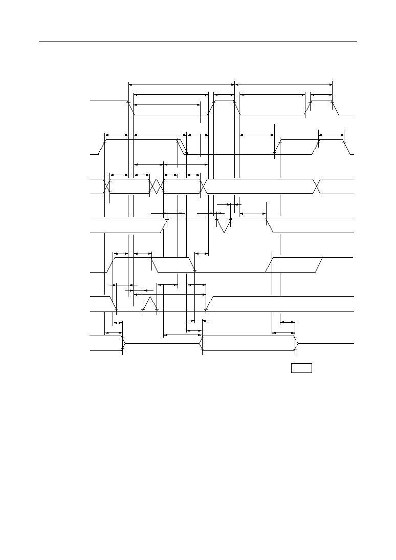
TIMING WAVEFORM
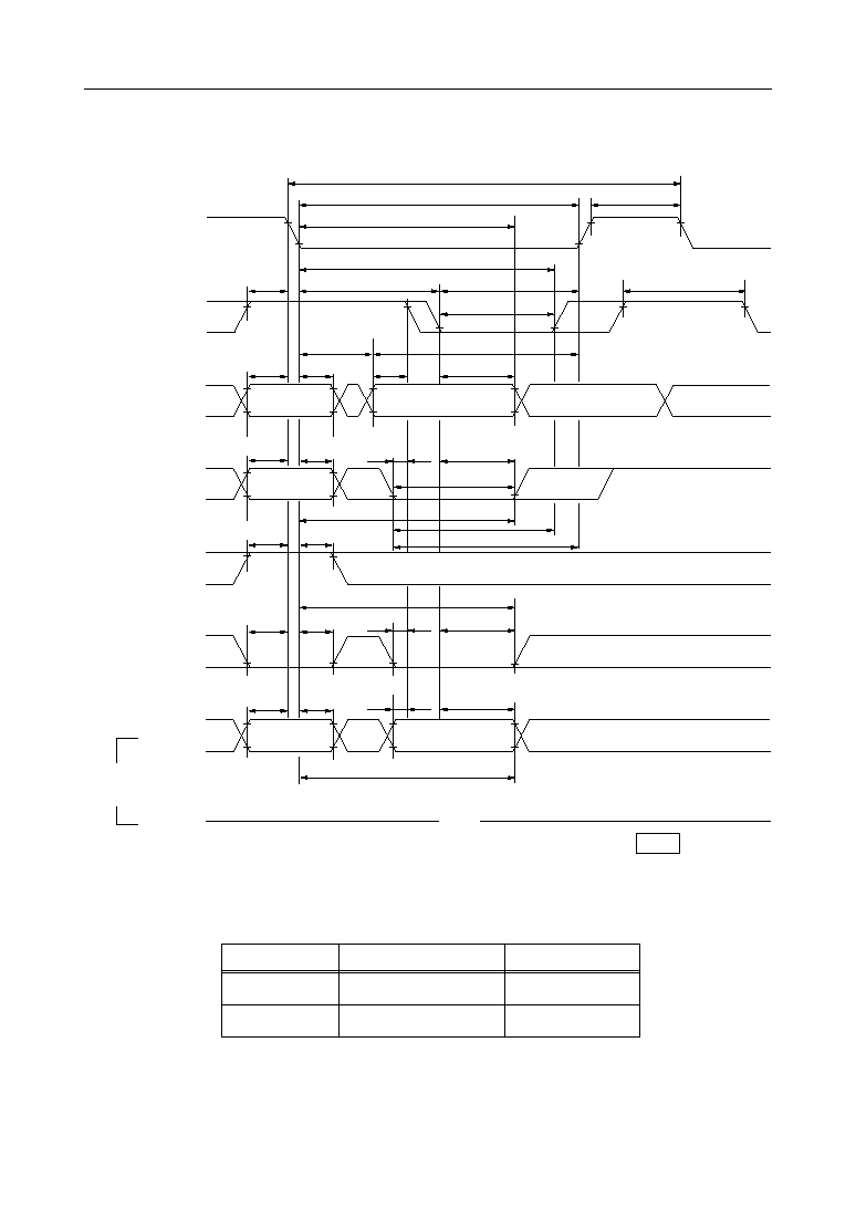
Read Cycle
"H" or "L"
RAS
CAS
A0 - A7
WB/WE
DT/OE
DSF
IN
OUT
W1/IO1 -
W8/IO8
V
IH
V
IL
≠
≠
,,
,
,
,,
V
IH
V
IL
≠
≠
V
IH
V
IL
≠
≠
V
IH
V
IL
≠
≠
V
IH
V
IL
≠
≠
V
IH
V
IL
≠
≠
V
IH
V
IL
≠
≠
V
OH
V
OL
≠
≠
t
RC
t
RAS
t
RP
t
AR
t
CSH
t
CRP
t
RCD
t
RSH
t
CPN
t
CAS
t
RAD
t
RAL
t
ASR
t
RAH
t
ASC
t
CAH
Row Address
Column Address
t
RCS
t
RCH
t
RRH
t
ROH
t
THS
t
THH
t
FSR
t
RFH
t
FHR
t
FSC
t
CFH
t
OEA
t
DZO
t
CAC
t
AA
t
RAC
t
OFF
t
OEZ
Open
Valid Data-out
MSM54C865
° Semiconductor
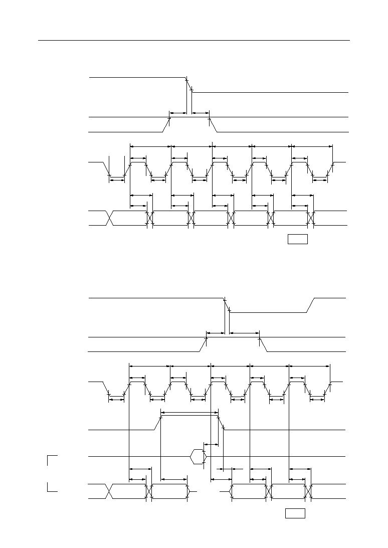
11/44
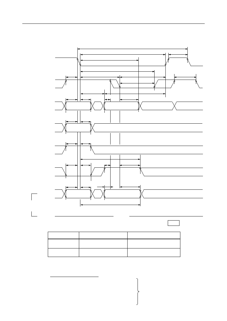
Write Cycle (Early Write)
"H" or "L"
RAS
CAS
A0 - A7
WB/WE
DT/OE
DSF
IN
OUT
W1/IO1 -
W8/IO8
V
IH
V
IL
≠
≠
V
IH
V
IL
≠
≠
V
IH
V
IL
≠
≠
V
IH
V
IL
≠
≠
V
IH
V
IL
≠
≠
V
IH
V
IL
≠
≠
V
IH
V
IL
≠
≠
V
OH
V
OL
≠
≠
,,
,
,,
,
t
RC
t
RAS
t
RP
t
AR
t
CSH
t
CRP
t
RCD
t
RSH
t
CAS
t
CPN
t
RAD
t
RAL
t
ASR
t
RAH
t
ASC
t
CAH
Row Address
Column Address
t
WSR
t
RWH
t
WCS
t
WCH
t
WP
t
WCR
t
CWL
t
RWL
t
THS
t
THH
t
FHR
t
FSR
t
RFH
t
FSC
t
CFH
t
MS
t
MH
t
DS
t
DH
WM1 Data
Valid Data-in
t
DHR
Open
*1
*1 WB/WE
0
1
W1/IO1 - W8/IO8
WM1 data
Don't Care
Cycle
Write per Bit
Normal Write
WM1 data:
0: Write Disable
1: Write Enable
MSM54C865
° Semiconductor
12/44
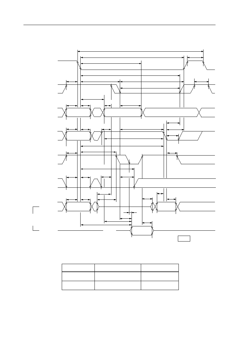
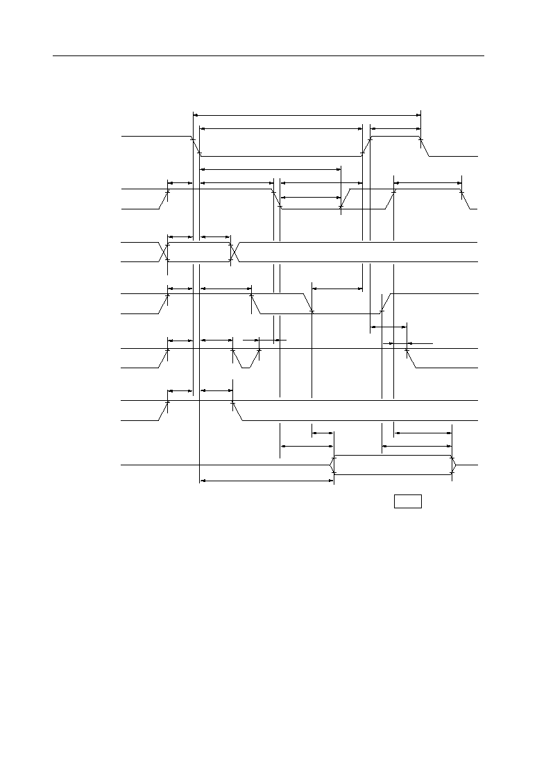
Write Cycle (OE Control)
"H" or "L"
RAS
CAS
A0 - A7
WB/WE
DT/OE
DSF
IN
OUT
W1/IO1 -
W8/IO8
V
IH
V
IL
≠
≠
V
IH
V
IL
≠
≠
V
IH
V
IL
≠
≠
V
IH
V
IL
≠
≠
V
IH
V
IL
≠
≠
V
IH
V
IL
≠
≠
V
IH
V
IL
≠
≠
V
OH
V
OL
≠
≠
,,
,
t
RC
t
RAS
t
RP
t
AR
t
CSH
t
CRP
t
RCD
t
RSH
t
CPN
t
CAS
t
RAD
t
RAL
t
ASR
t
RAH
t
ASC
t
CAH
Row Address
Column Address
t
CWL
t
RWL
t
WP
t
WSR
t
RWH
*1
t
WCR
t
OEH
t
THS
t
FHR
t
FSR
t
RFH
t
FSC
t
CFH
t
MS
t
MH
t
DS
t
DH
WM1 Data
Valid Data-in
t
DHR
Open
*1 WB/WE
0
1
W1/IO1 - W8/IO8
WM1 data
Don't Care
Cycle
Write per Bit
Normal Write
WM1 data:
0: Write Disable
1: Write Enable
MSM54C865
° Semiconductor
13/44
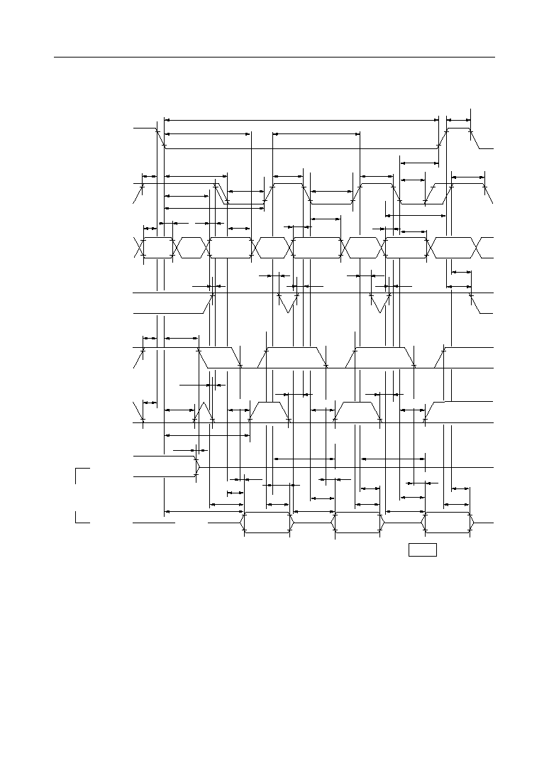
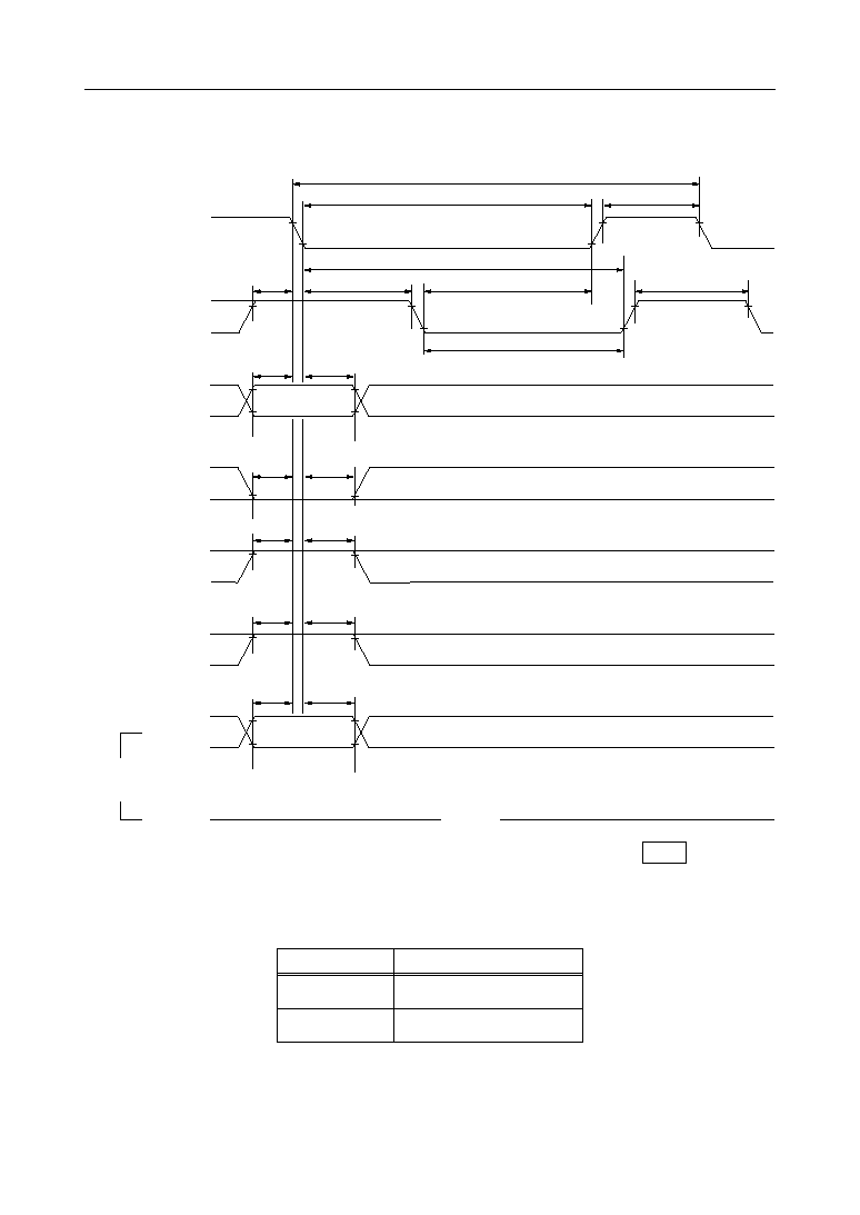
Read Modify Write Cycle
"H" or "L"
RAS
CAS
A0 - A7
WB/WE
DT/OE
DSF
IN
OUT
W1/IO1 -
W8/IO8
V
IH
V
IL
≠
≠
V
IH
V
IL
≠
≠
V
IH
V
IL
≠
≠
V
IH
V
IL
≠
≠
V
IH
V
IL
≠
≠
V
IH
V
IL
≠
≠
V
IH
V
IL
≠
≠
V
OH
V
OL
≠
≠
,,
,
t
RWC
t
RAS
t
RP
t
AR
t
CSH
t
CRP
t
RCD
t
RSH
t
CPN
t
RAD
t
ASR
t
RAH
t
ASC
t
CAH
Row Address
Column Address
t
WSR
t
RWH
t
RCS
t
CWD
t
CWL
t
RWL
t
WP
*1
t
AWD
t
RWD
t
THS
t
THH
t
OEH
t
FHR
t
FSR
t
RFH
t
FSC
t
CFH
t
DZC
t
MS
t
MH
t
DZO
t
OED
t
DS
t
DH
WM1 Data
Valid
Data-in
t
OEA
t
CAC
t
AA
t
RAC
t
OEZ
Open
Valid
Data-out
t
CAS
*1 WB/WE
0
1
W1/IO1 - W8/IO8
WM1 data
Don't Care
Cycle
Write per Bit
Normal Write
WM1 data:
0: Write Disable
1: Write Enable
MSM54C865
° Semiconductor
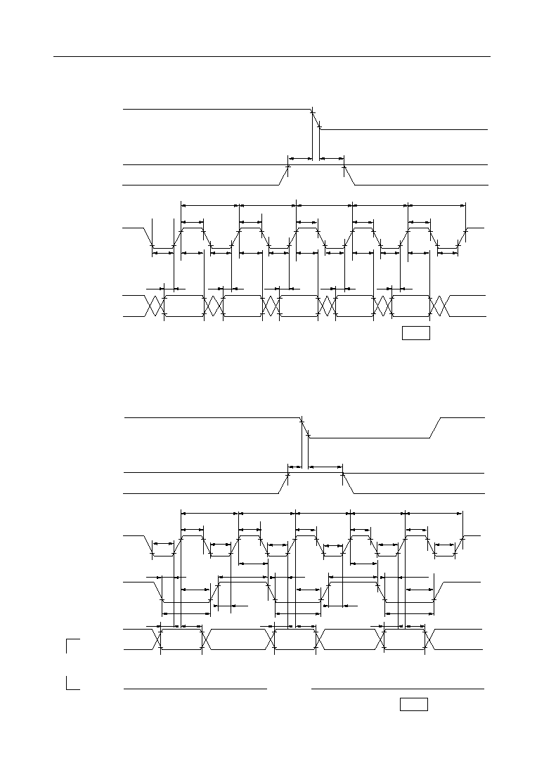
14/44
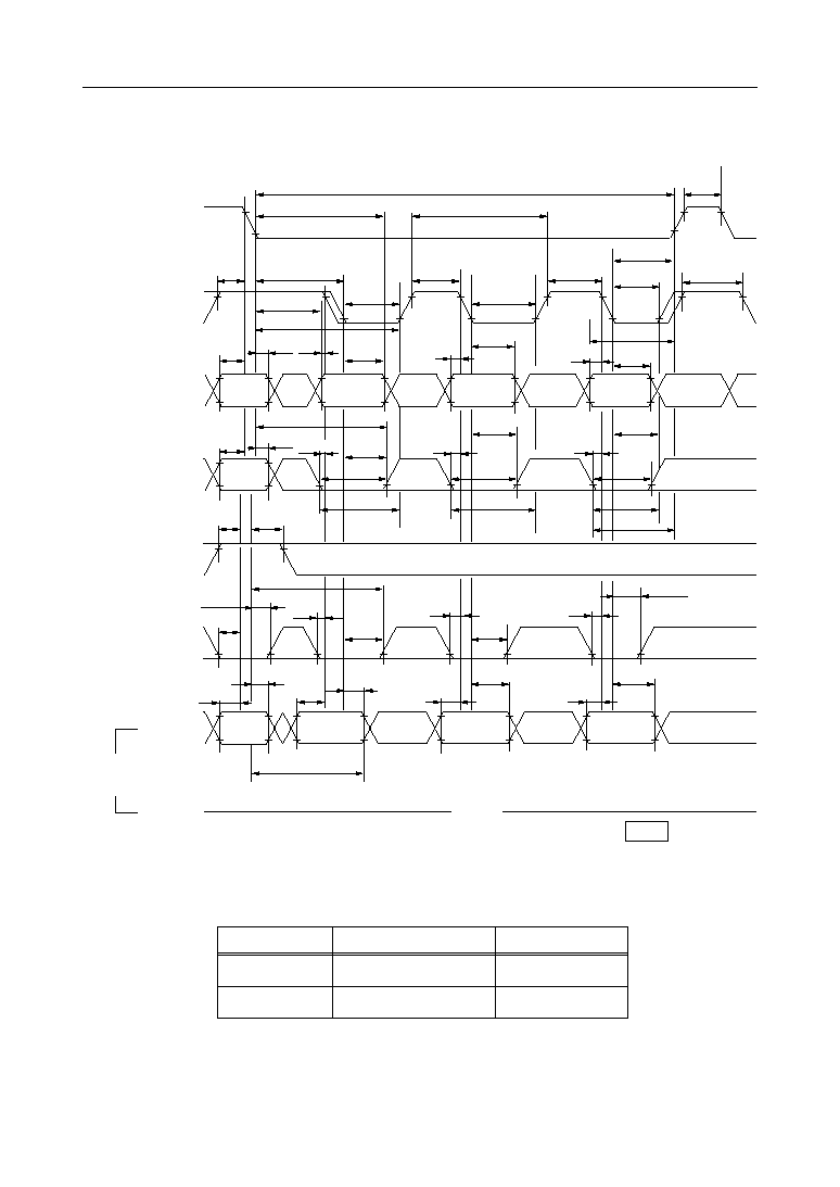
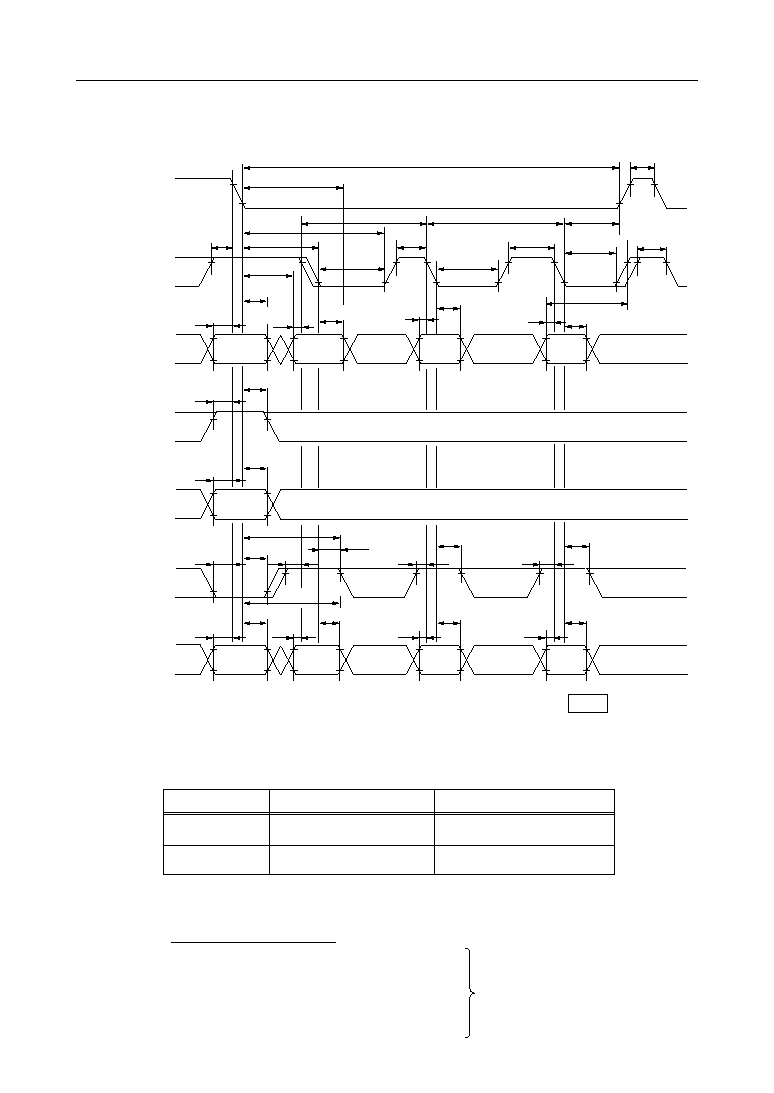
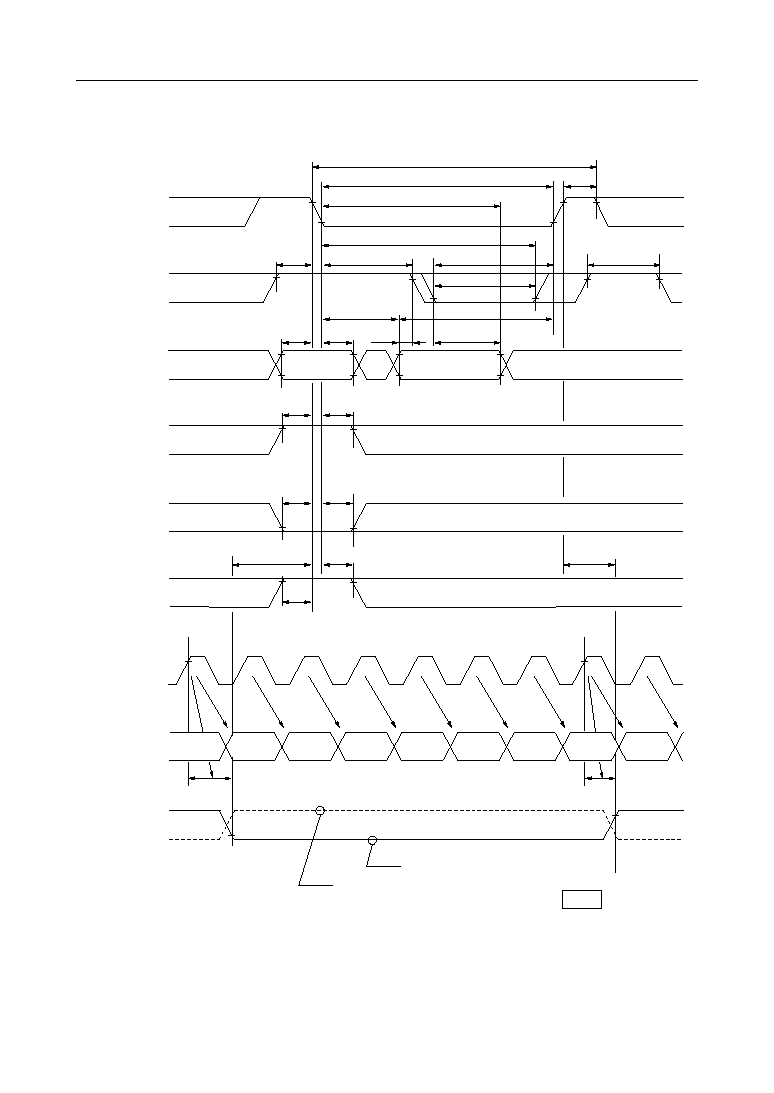
Fast Page Mode Read Cycle
"H" or "L"
RAS
CAS
A0 - A7
WB/WE
DT/OE
DSF
IN
OUT
W1/IO1 -
W8/IO8
V
IH
V
IL
≠
≠
V
IH
V
IL
≠
≠
V
IH
V
IL
≠
≠
V
IH
V
IL
≠
≠
V
IH
V
IL
≠
≠
V
IH
V
IL
≠
≠
V
IH
V
IL
≠
≠
V
OH
V
OL
≠
≠
,
,
,
,
,
,
t
RASP
t
RP
t
AR
t
PC
t
CRP
t
RCD
t
CAS
t
CP
t
CAS
t
CP
t
RSH
t
CAS
t
CPN
t
RAD
t
CSH
t
ASR
t
RAH
t
ASC
t
CAH
t
ASC
t
CAH
t
RAL
t
ASC
t
CAH
Row
Address
Column
Address 1
Column
Address 2
Column
Address n
t
RCS
t
RCH
t
RCS
t
RCH
t
RCS
t
RCH
t
RRH
t
THS
t
THH
t
FSC
t
FSR
t
THH
t
CFH
t
FSC
t
CFH
t
FSC
t
CFH
t
FHR
t
DZO
t
CPA
t
CPA
t
OEA
t
CAC
t
AA
t
RAC
t
OFF
t
OEZ
t
OEA
t
CAC
t
AA
t
OFF
t
OEZ
t
OEA
t
CAC
t
AA
t
OFF
t
OEZ
Open
Data-out 1
Data-out 2
Data-out n
MSM54C865
° Semiconductor
15/44
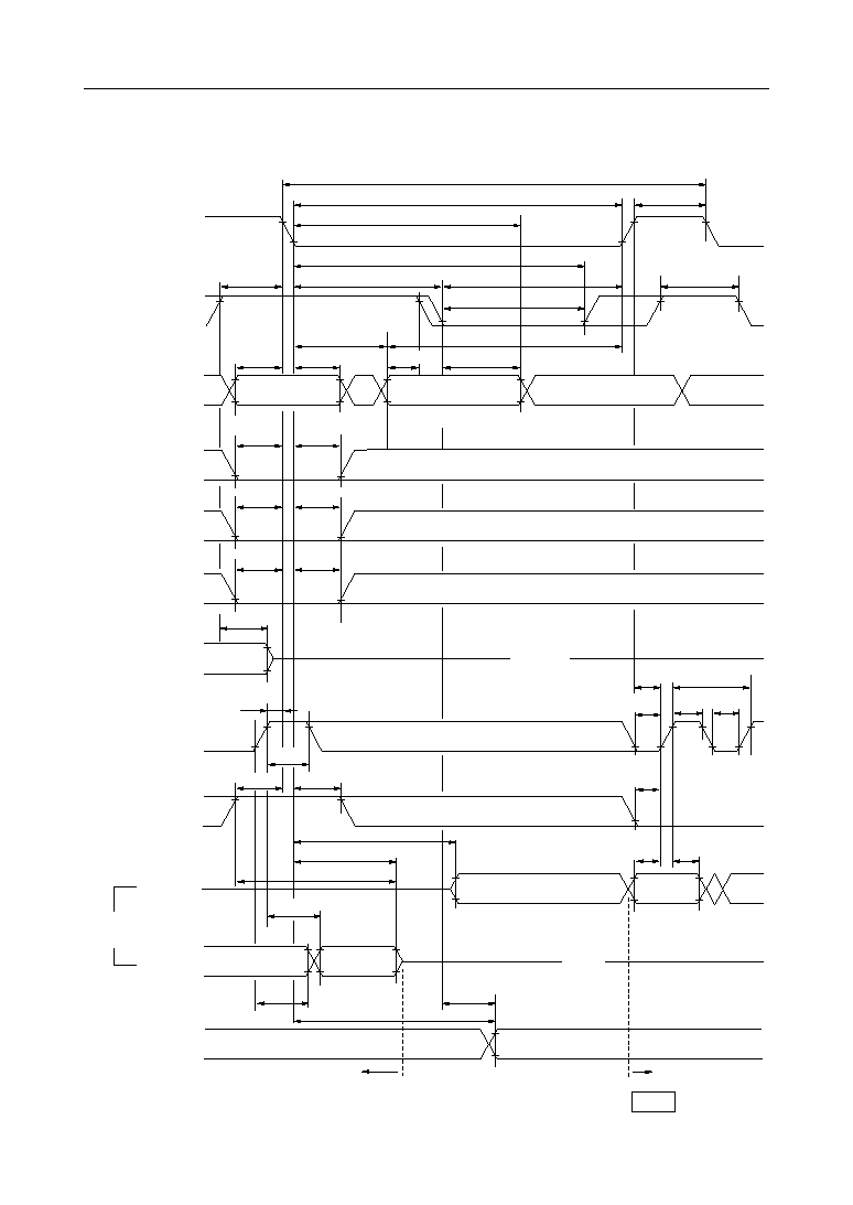
Fast Page Mode Write Cycle (Early Write)
"H" or "L"
RAS
CAS
A0 - A7
WB/WE
DT/OE
DSF
IN
OUT
W1/IO1 -
W8/IO8
V
IH
V
IL
≠
≠
V
IH
V
IL
≠
≠
V
IH
V
IL
≠
≠
V
IH
V
IL
≠
≠
V
IH
V
IL
≠
≠
V
IH
V
IL
≠
≠
V
IH
V
IL
≠
≠
V
OH
V
OL
≠
≠
,
,
,,,
,
t
RASP
t
RP
t
AR
t
PC
t
CRP
t
RCD
t
CAS
t
CP
t
CAS
t
CP
t
CAS
t
RSH
t
CPN
t
RAD
t
CSH
t
ASR
t
RAH
t
ASC
t
CAH
t
ASC
t
CAH
t
ASC
t
RAL
t
CAH
Row
Address
Column
Address 1
Column
Address 2
Column
Address n
t
WCR
t
WSR
t
RWH
t
WCS
t
WCH
t
WP
t
WCS
t
WCH
t
WP
t
WCS
t
WCH
t
WP
t
THS
t
THH
t
CWL
t
CWL
t
CWL
t
RWL
t
FHR
t
RFH
t
FSR
t
FSC
t
CFH
t
FSC
t
CFH
t
FSC
t
CFH
t
MH
t
MS
t
DS
t
DH
t
DS
t
DH
t
DS
t
DH
t
DHR
WM1
Data
Data-in 1
Data-in 2
Data-in n
Open
*1
*1 WB/WE
0
1
W1/IO1 - W8/IO8
WM1 data
Don't Care
Cycle
Write per Bit
Normal Write
WM1 data:
0: Write Disable
1: Write Enable
MSM54C865
° Semiconductor
16/44
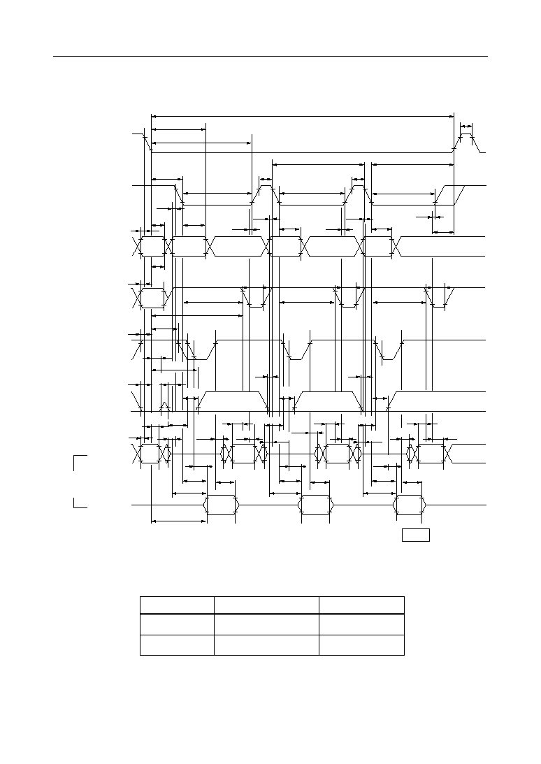
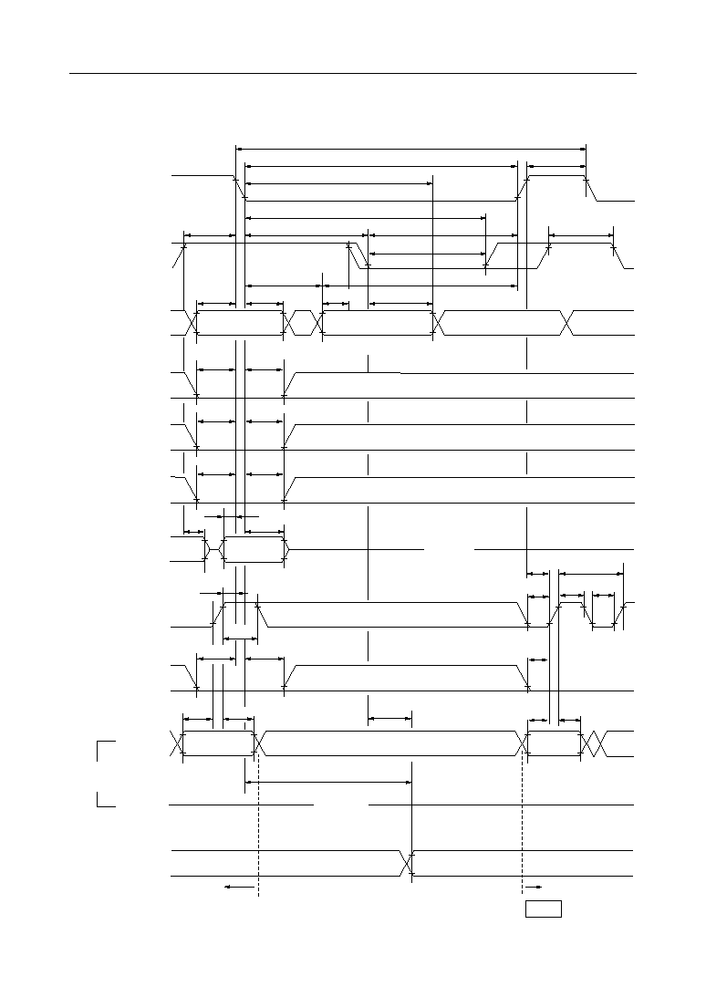
Fast Page Mode Read Modify Write Cycle
"H" or "L"
RAS
CAS
A0 - A7
WB/WE
DT/OE
DSF
IN
OUT
W1/IO1 -
W8/IO8
V
IH
V
IL
≠
≠
V
IH
V
IL
≠
≠
V
IH
V
IL
≠
≠
V
IH
V
IL
≠
≠
V
IH
V
IL
≠
≠
V
IH
V
IL
≠
≠
V
IH
V
IL
≠
≠
V
OH
V
OL
≠
≠
,
,
,
t
RASP
t
RP
t
AR
t
CSH
t
PRWC
t
RSH
t
RCD
t
CAS
t
CP
t
CAS
t
CP
t
CAS
t
ASC
t
ASR
t
RAH
t
CAH
t
CWL
t
ASC
t
CAH
t
CWL
t
ASC
t
CAH
t
CWL
t
RWL
Row
Address
Column
Address 1
Column
Address 2
Column
Address n
t
RWH
t
WSR
t
WP
t
WP
t
WP
*1
t
CWD
t
CWD
t
CWD
t
RWD
t
THS
t
THH
t
RFH
t
FHR
t
FSR
t
FSC
t
FSC
t
FSC
t
CFH
t
CFH
t
CFH
t
MH
t
MS
t
DZO
t
DZC
t
DS
t
OED
t
DH
t
DZO
t
DZC
t
OED
t
DS
t
DH
t
DZO
t
DZC
t
DS
t
OED
t
DH
WM1
Data
Data-
in 1
Data-
in 2
Data-
in n
t
OEA
t
CAC
t
AA
t
RAC
t
OEZ
t
OEA
t
CAC
t
AA
t
OEZ
t
OEA
t
CAC
t
OEZ
t
AA
Data-
out 1
Data-
out 2
Data-
out n
*1 WB/WE
0
1
W1/IO1 - W8/IO8
WM1 data
Don't Care
Cycle
Write per Bit
Normal Write
WM1 data:
0: Write Disable
1: Write Enable
MSM54C865
° Semiconductor
17/44
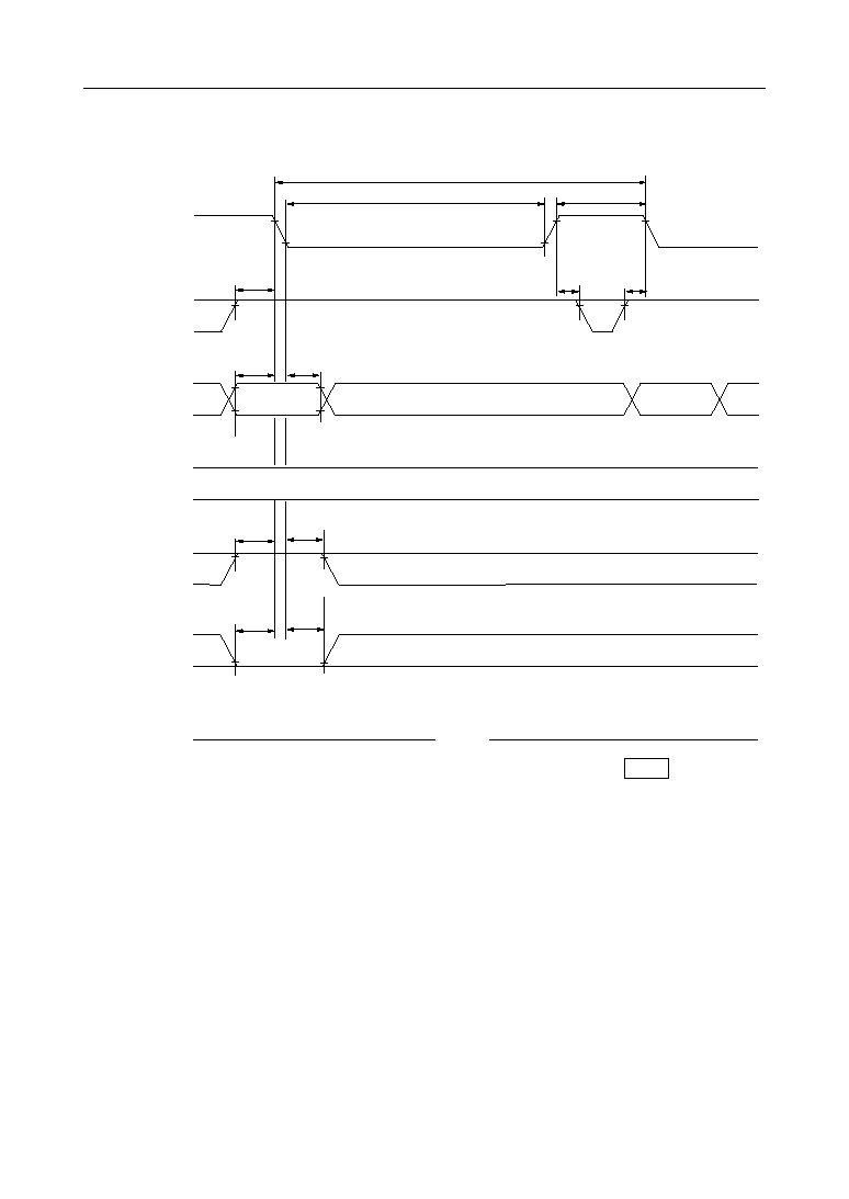
RAS Only Refresh Cycle
"H" or "L"
RAS
CAS
A0 - A7
WB/WE
DT/OE
DSF
W1/IO1 -
W8/IO8
V
IH
V
IL
≠
≠
V
IH
V
IL
≠
≠
V
IH
V
IL
≠
≠
V
IH
V
IL
≠
≠
V
IH
V
IL
≠
≠
V
IH
V
IL
≠
≠
,,,
,,,
V
OH
V
OL
≠
≠
t
RC
t
RAS
t
RP
t
CRP
t
RPC
t
CRP
t
ASR
t
RAH
Row Address
t
THS
t
THH
t
FSR
t
RFH
Open
MSM54C865
° Semiconductor
18/44
CAS before RAS Refresh Cycle
"H" or "L"
RAS
CAS
WB/WE
DT/OE
DSF
W1/IO1 -
W8/IO8
V
IH
V
IL
≠
≠
V
IH
V
IL
≠
≠
V
IH
V
IL
≠
≠
V
IH
V
IL
≠
≠
V
IH
V
IL
≠
≠
V
OH
V
OL
≠
≠
,,,
,
t
RP
t
RC
t
RP
t
RAS
t
RPC
t
CSR
t
CPN
t
CHR
t
OFF
Open
Note: A0 - A7 = Don't care ("H" or "L")
MSM54C865
° Semiconductor
19/44
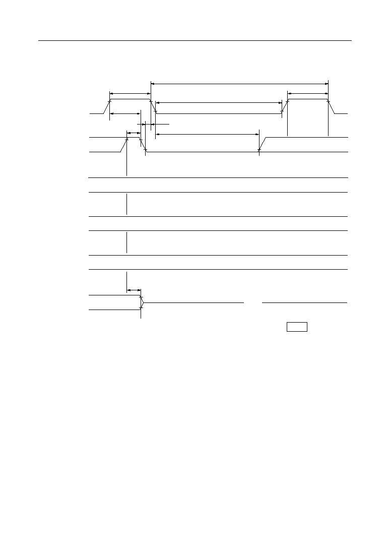
Hidden Refresh Cycle
"H" or "L"
RAS
CAS
A0 - A7
WB/WE
DT/OE
DSF
W1/IO1 -
W8/IO8
V
IH
V
IL
≠
≠
V
IH
V
IL
≠
≠
V
IH
V
IL
≠
≠
V
IH
V
IL
≠
≠
V
IH
V
IL
≠
≠
V
IH
V
IL
≠
≠
V
OH
V
OL
≠
≠
,,
,
,
,
t
RC
t
RC
t
RAS
t
AR
t
RP
t
RAS
t
RP
t
CRP
t
RCD
t
RSH
t
CHR
t
CPN
t
RAD
t
RAL
t
ASR
t
RAH
t
ASC
t
CAH
Row Address
Column
Address
t
RCS
t
RRH
t
WSR
t
RWH
t
THS
t
THH
t
ROH
t
FSR
t
RFH
t
FSC
t
CFH
t
FHR
t
OEZ
t
OFF
t
OEA
t
CAC
t
AA
t
OFF
t
OEZ
Valid Data-out
MSM54C865
° Semiconductor
20/44
Load Color Register Cycle
"H" or "L"
RAS
CAS
A0 - A7
WB/WE
DT/OE
DSF
IN
OUT
W1/IO1 -
W8/IO8
V
IH
V
IL
≠
≠
V
IH
V
IL
≠
≠
V
IH
V
IL
≠
≠
V
IH
V
IL
≠
≠
V
IH
V
IL
≠
≠
V
IH
V
IL
≠
≠
V
IH
V
IL
≠
≠
V
OH
V
OL
≠
≠
,,,
,,
t
RC
t
RAS
t
RP
t
CRP
t
CSH
t
RCD
t
RSH
t
CAS
t
CPN
t
ASR
t
RAH
Row Address
t
WSR
t
RWH
t
CWL
t
RWL
t
WP
t
WCR
t
THS
t
WCH
t
OEH
t
FSR
t
RFH
t
DHR
t
DS
t
DH
t
DS
t
DH
Color Data-in
(Delayed Write)
Color Data-in
(Early Write)
MSM54C865
° Semiconductor
21/44
Read Color Register Cycle
"H" or "L"
RAS
CAS
A0 - A7
WB/WE
DT/OE
DSF
V
IH
V
IL
≠
≠
V
IH
V
IL
≠
≠
V
IH
V
IL
≠
≠
V
IH
V
IL
≠
≠
V
IH
V
IL
≠
≠
V
IH
V
IL
≠
≠
,
,
,
,,
V
OH
V
OL
≠
≠
W1/IO1 -
W8/IO8
t
RC
t
RAS
t
RP
t
CSH
t
CRP
t
RCD
t
RSH
t
CAS
t
CPN
t
ASR
t
RAH
Row Address
t
THS
t
THH
t
ROH
t
RRH
t
RCH
t
WSR
t
RWH
t
RCS
t
FSR
t
RFH
t
OEA
t
CAC
t
OFF
t
OEZ
t
RAC
Valid Data-out
MSM54C865
° Semiconductor
22/44
Flash Write Cycle
"H" or "L"
RAS
CAS
A0 - A7
WB/WE
DT/OE
DSF
IN
OUT
W1/IO1 -
W8/IO8
V
IH
V
IL
≠
≠
V
IH
V
IL
≠
≠
V
IH
V
IL
≠
≠
V
IH
V
IL
≠
≠
V
IH
V
IL
≠
≠
V
IH
V
IL
≠
≠
V
IH
V
IL
≠
≠
V
OH
V
OL
≠
≠
,,
,,
t
RC
t
RAS
t
RP
t
CSH
t
CRP
t
RCD
t
RSH
t
CPN
t
CAS
t
ASR
t
RAH
Row Address
t
WSR
t
RWH
t
TLS
t
TLH
t
FSR
t
RFH
t
MS
t
MH
WM1 Data
Open
WM1 Data
0
1
Cycle
Flash Write Disable
Flash Write Enable
MSM54C865
° Semiconductor
23/44
Block Write Cycle
"H" or "L"
RAS
CAS
A0 - A7
WB/WE
DT/OE
DSF
IN
OUT
W1/IO1 -
W8/IO8
V
IH
V
IL
≠
≠
V
IH
V
IL
≠
≠
V
IH
V
IL
≠
≠
V
IH
V
IL
≠
≠
V
IH
V
IL
≠
≠
V
IH
V
IL
≠
≠
V
IH
V
IL
≠
≠
V
OH
V
OL
≠
≠
,,,
,
t
RC
t
RAS
t
RP
t
AR
t
CSH
t
CRP
t
RCD
t
RSH
t
CAS
t
CPN
t
RAD
t
RAL
t
ASR
t
RAH
t
ASC
t
CAH
Row Address
Column Address
(A2C - A7C)
t
WSR
t
RWH
*1
t
THS
t
THH
t
FHR
t
FSR
t
RFH
t
FSC
t
CFH
t
MS
t
MH
t
DS
t
DH
t
DHR
*2
*3
Open
*1 WB/WE
0
1
*2 W1/IO1 - W8/IO8
WM1 data
Don't Care
Cycle
Masked Block Write
Block Write (Non Mask)
WM1 data:
0: Write Disable
1: Write Enable
*3) COLUMN SELECT
W1/IO1 ≠ Column 0 (A1C = 0, A0C = 0)
W2/IO2 ≠ Column 1 (A1C = 0, A0C = 1)
W3/IO3 ≠ Column 2 (A1C = 1, A0C = 0)
W4/IO4 ≠ Column 3 (A1C = 1, A0C = 1)
Wn/IOn
= 0 : Disable
= 1 : Enable
MSM54C865
° Semiconductor
24/44
Fast Page Mode Block Write Cycle
"H" or "L"
RAS
CAS
A0 - A7
DT/OE
WB/WE
DSF
V
IH
V
IL
≠
≠
V
IH
V
IL
≠
≠
V
IH
V
IL
≠
≠
V
IH
V
IL
≠
≠
V
IH
V
IL
≠
≠
V
IH
V
IL
≠
≠
,,,
,
,
,
,
V
IH
V
IL
≠
≠
W1/IO1 -
W8/IO8
t
RASP
t
RP
t
AR
t
CRP
t
CSH
t
RCD
t
PC
t
CAS
t
CP
t
PC
t
RSH
t
CAS
t
CP
t
CAS
t
CPN
t
RAD
t
RAH
t
ASR
t
ASC
t
CAH
t
ASC
t
CAH
t
ASC
t
CAH
t
RAL
Row
Address
A2C -
A7C
A2C -
A7C
A2C -
A7C
t
THS
t
THH
t
WSR
t
RWH
*1
t
FHR
t
FSR
t
MH
t
RFH
t
FSC
t
CFH
t
FSC
t
CFH
t
FSC
t
CFH
t
DHR
t
MS
t
DS
t
DH
t
DS
t
DH
t
DS
t
DH
*2
*3
*3
*3
*1 WB/WE
0
1
*2 W1/IO1 - W8/IO8
WM1 data
Don't Care
Cycle
Masked Block Write
Block Write (Non Mask)
WM1 data:
0: Write Disable
1: Write Enable
*3) COLUMN SELECT
W1/IO1 ≠ Column 0 (A1C = 0, A0C = 0)
W2/IO2 ≠ Column 1 (A1C = 0, A0C = 1)
W3/IO3 ≠ Column 2 (A1C = 1, A0C = 0)
W4/IO4 ≠ Column 3 (A1C = 1, A0C = 1)
Wn/IOn
= 0 : Disable
= 1 : Enable
MSM54C865
° Semiconductor
25/44
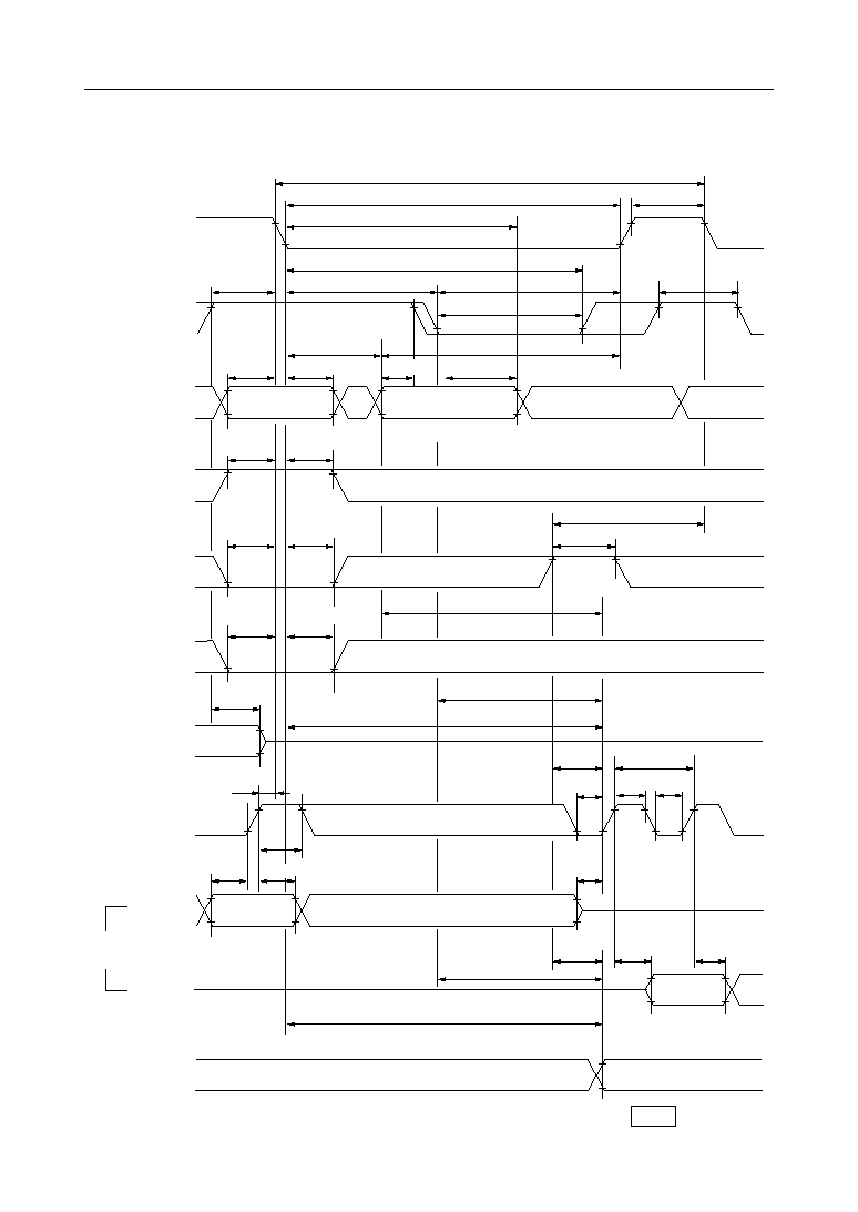
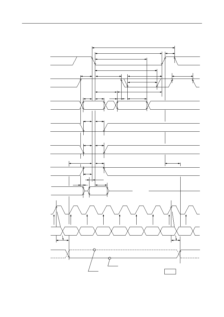
Read Transfer Cycle (Previous Transfer is Write Transfer Cycle)
,
"H" or "L"
RAS
CAS
A0 - A7
WB/WE
DT/OE
DSF
V
IH
V
IL
≠
≠
V
IH
V
IL
≠
≠
V
IH
V
IL
≠
≠
V
IH
V
IL
≠
≠
V
IH
V
IL
≠
≠
V
IH
V
IL
≠
≠
W1/IO1 -
W8/IO8
,
V
OH
V
OL
≠
≠
SC
V
IH
V
IL
≠
≠
IN
V
IH
V
IL
≠
≠
OUT
V
OH
V
OL
≠
≠
SIO1 -
SIO8
QSF
V
OH
V
OL
≠
≠
t
RC
t
RAS
t
RP
t
AR
t
CSH
t
CRP
t
RCD
t
RSH
t
CPN
t
CAS
t
ASR
t
RAH
t
RAD
t
ASC
t
CAH
t
RAL
Row Address
SAM Start Address
A0 - A7: TAP
t
WSR
t
RWH
t
TRP
t
TLS
t
TLH
t
TP
t
FSR
t
RFH
t
ASD
t
OFF
t
RSD
t
CSD
t
SRS
t
SC
t
TSD
t
SCC
t
SCP
t
SC
t
SCP
Inhibit Rising Transient
t
SDS
t
SDH
t
SZS
Valid Data-in
t
CQD
t
TQD
t
SCA
t
SOH
Valid
Data-out
t
RQD
TAP MSB (A7)
Note: SE = V
IL
MSM54C865
° Semiconductor
26/44
Real Time Read Transfer Cycle
"H" or "L"
RAS
CAS
A0 - A7
WB/WE
DT/OE
DSF
V
IH
V
IL
≠
≠
V
IH
V
IL
≠
≠
V
IH
V
IL
≠
≠
V
IH
V
IL
≠
≠
V
IH
V
IL
≠
≠
V
IH
V
IL
≠
≠
W1/IO1 -
W8/IO8
V
OH
V
OL
≠
≠
SC
V
IH
V
IL
≠
≠
IN
V
IH
V
IL
≠
≠
OUT
V
OH
V
OL
≠
≠
SIO1 -
SIO8
QSF
V
OH
V
OL
≠
≠
Note: SE = V
IL
,
,,
,,,
t
RC
t
RAS
t
RP
t
AR
t
CSH
t
CRP
t
RCD
t
RSH
t
CAS
t
CPN
t
RAD
t
ASR
t
RAH
t
ASC
t
CAH
t
RAL
Row Address
SAM Start Address
A0 - A7: TAP
t
WSR
t
RWH
t
ATH
t
CTH
t
TRP
t
TLS
t
RTH
t
TP
t
FSR
t
RFH
t
OFF
t
SCC
t
SC
t
SCP
t
TSL
t
TSD
t
SCA
t
SOH
t
TQD
Open
t
SCA
t
SOH
Valid
Data-out
Valid
Data-out
Valid
Data-out
Valid
Data-out
Valid
Data-out
Previous Row Data
New Row Data
TAP MSB (A7)
MSM54C865
° Semiconductor
27/44
Split Read Transfer Cycle
,
"H" or "L"
RAS
CAS
A0 - A7
WB/WE
DT/OE
DSF
V
IH
V
IL
≠
≠
V
IH
V
IL
≠
≠
V
IH
V
IL
≠
≠
V
IH
V
IL
≠
≠
V
IH
V
IL
≠
≠
V
IH
V
IL
≠
≠
SC
V
IH
V
IL
≠
≠
QSF
V
OH
V
OL
≠
≠
Note: SE = V
IL
,
,
,
,,
...............
...............
V
OH
V
OL
≠
≠
SIO1 -
SIO8
t
RC
t
RAS
t
RP
t
AR
t
CRP
t
CSH
t
RCD
t
RSH
t
CPN
t
CAS
t
RAD
t
RAL
t
ASR
t
RAH
t
ASC
t
CAH
Row Address
SAM Start
Address (n)
A0 - A6: TAP
t
WSR
t
RWH
t
TLS
t
TLH
t
STS
t
RFH
t
STH
t
FSR
255
(127)
n
(n+128)
n+1
(n+129)
n+2
(n+130)
125
(253)
126
(254)
n+128
(n)
127
(255)
t
SQD
254
(126)
255
(127)
n
(n+128)
n+1
(n+129)
n+2
(n+130)
125
(253)
126
(254)
127
(255)
t
SQD
Lower SAM 0 to 127
Upper SAM 128 to 255
MSM54C865
° Semiconductor
28/44
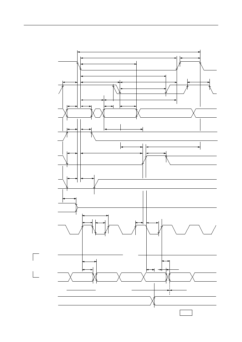
Pseudo Write Transfer Cycle
"H" or "L"
RAS
CAS
A0 - A7
WB/WE
DT/OE
DSF
V
IH
V
IL
≠
≠
V
IH
V
IL
≠
≠
V
IH
V
IL
≠
≠
V
IH
V
IL
≠
≠
V
IH
V
IL
≠
≠
V
IH
V
IL
≠
≠
SC
V
IH
V
IL
≠
≠
QSF
V
OH
V
OL
≠
≠
SIO1 -
SIO8
,
V
OH
V
OL
≠
≠
W1/IO1 -
W8/IO8
V
OH
V
OL
≠
≠
OUT
IN
V
IH
V
IL
≠
≠
SE
V
IH
V
IL
≠
≠
t
RC
t
RAS
t
RP
t
AR
t
CSH
t
CRP
t
RCD
t
RSH
t
CAS
t
CPN
t
ASR
t
RAH
t
RAD
t
ASC
t
RAL
t
CAH
Row Address
SAM Start Address
A0 - A7: TAP
t
WSR
t
RWH
t
TLS
t
TLH
t
FSR
t
RFH
t
OFF
Open
t
SRD
t
SCC
t
SCP
t
SC
t
SCP
t
SRS
Inhibit Rising Transient
t
SC
t
ESR
t
REH
t
SWS
t
SDD
t
SDZ
t
SEZ
t
SDS
t
SDH
Valid
Data-in
t
SCA
Valid Data-out
Valid
Data-out
Open
t
SOH
t
RQD
t
CQD
TAP MSB (A7)
Serial Output Data
Serial Input Data
MSM54C865
° Semiconductor
29/44
Write Transfer Cycle
"H" or "L"
RAS
CAS
A0 - A7
WB/WE
DT/OE
DSF
V
IH
V
IL
≠
≠
V
IH
V
IL
≠
≠
V
IH
V
IL
≠
≠
V
IH
V
IL
≠
≠
V
IH
V
IL
≠
≠
V
IH
V
IL
≠
≠
SC
V
IH
V
IL
≠
≠
QSF
V
OH
V
OL
≠
≠
SIO1 ~
SIO8
V
OH
V
OL
≠
≠
W1/IO1 -
W8/IO8
V
OH
V
OL
≠
≠
OUT
IN
V
IH
V
IL
≠
≠
SE
V
IH
V
IL
≠
≠
,
t
RC
t
RAS
t
RP
t
AR
t
CRP
t
CSH
t
RCD
t
RSH
t
CAS
t
CPN
t
RAD
t
ASR
t
RAH
t
ASC
t
RAL
t
CAH
Row Address
SAM Start Address
A0 - A7: TAP
t
WSR
t
RWH
t
TLS
t
TLH
t
FSR
t
RFH
t
MS
t
OFF
t
MH
WM1 Data
Open
t
SRD
t
SCC
t
SCP
t
SC
t
SCP
t
SRS
Inhibit Rising Transient
t
SC
t
ESR
t
REH
t
SWS
t
SDS
t
SDH
Valid Data-in
t
CQD
t
SDS
t
SDH
Valid
Data-in
Valid
Data-in
t
RQD
Open
TAP MSB (A7)
Previous
Row Data
New Row Data
WM1 data: 0: Transfer Disable
1: Transfer Enable
MSM54C865
° Semiconductor
30/44
Split Write Transfer Cycle
,
"H" or "L"
RAS
CAS
A0 - A7
WB/WE
DT/OE
DSF
V
IH
V
IL
≠
≠
V
IH
V
IL
≠
≠
V
IH
V
IL
≠
≠
V
IH
V
IL
≠
≠
V
IH
V
IL
≠
≠
V
IH
V
IL
≠
≠
SC
V
IH
V
IL
≠
≠
QSF
V
OH
V
OL
≠
≠
Note: SE = V
IL
SIO1 -
SIO8
V
OH
V
OL
≠
≠
W1/IO1 -
W8/IO8
V
IH
V
IL
≠
≠
,
,
,
,,
...............
...............
t
RC
t
RAS
t
RP
t
AR
t
CSH
t
CRP
t
RCD
t
RSH
t
CPN
t
CAS
t
RAD
t
RAL
t
ASR
t
RAH
t
ASC
t
CAH
Row Address
SAM Start
Address (n)
A0 - A6: TAP
t
WSR
t
RWH
t
TLS
t
TLH
t
STS
t
RFH
t
STH
t
FSR
t
MS
t
OFF
t
MH
Open
WM1 Data
t
SQD
t
SQD
255
(127)
n
(n+128)
n+1
(n+129)
n+2
(n+130)
125
(253)
126
(254)
n+128
(n)
127
(255)
255
(127)
n
(n+128)
n+1
(n+129)
n+2
(n+130)
125
(253)
126
(254)
n+128
(n)
127
(255)
Lower SAM 0 to 127
Upper SAM 128 to 255
MSM54C865
° Semiconductor
31/44
Serial Read Cycle (SE = V
IL
)
Serial Read Cycle (SE Controlled Outputs)
"H" or "L"
RAS
DT/OE
V
IH
V
IL
≠
≠
V
IH
V
IL
≠
≠
SC
V
IH
V
IL
≠
≠
Note: SE = V
IL
,
,,
V
OH
V
OL
≠
≠
SIO1 -
SIO8
t
THS
t
THH
t
SCC
t
SCC
t
SCC
t
SCC
t
SCC
t
SC
t
SC
t
SC
t
SC
t
SC
t
SCP
t
SCP
t
SCP
t
SCP
t
SCP
t
SCP
t
SCA
t
SCA
t
SCA
t
SCA
t
SCA
t
SOH
t
SOH
t
SOH
t
SOH
t
SOH
Valid
Data-out
Valid
Data-out
Valid
Data-out
Valid
Data-out
Valid
Data-out
Valid
Data-out
,
"H" or "L"
RAS
DT/OE
V
IH
V
IL
≠
≠
V
IH
V
IL
≠
≠
SC
V
IH
V
IL
≠
≠
,,
,
SE
V
IH
V
IL
≠
≠
IN
OUT
V
IH
V
IL
≠
≠
V
OH
V
OL
≠
≠
SIO1 -
SIO8
t
THS
t
THH
t
SCC
t
SCC
t
SCC
t
SCC
t
SCC
t
SC
t
SC
t
SC
t
SC
t
SC
t
SCP
t
SCP
t
SCP
t
SCP
t
SCP
t
SCP
t
SEP
t
SZE
t
SCA
t
SOH
t
SEZ
t
SEA
t
SCA
t
SCA
t
SOH
t
SCA
t
SOH
Open
Valid
Data-out
Valid
Data-out
Valid
Data-out
Valid
Data-out
Valid
Data-out
MSM54C865
° Semiconductor
32/44
Serial Write Cycle (SE = V
IL
)
Serial Write Cycle (SE Controlled Inputs)
"H" or "L"
RAS
DT/OE
V
IH
V
IL
≠
≠
V
IH
V
IL
≠
≠
SC
V
IH
V
IL
≠
≠
Note: SE = V
IL
,
,
V
IH
V
IL
≠
≠
SIO1 -
SIO8
t
THS
t
THH
t
SCC
t
SCC
t
SCC
t
SCC
t
SCC
t
SC
t
SC
t
SC
t
SC
t
SC
t
SDH
t
SDH
t
SDH
t
SDH
t
SDH
t
SCP
t
SCP
t
SCP
t
SCP
t
SCP
t
SCP
t
SDS
t
SDS
t
SDS
t
SDS
t
SDS
Valid
Data-in
Valid
Data-in
Valid
Data-in
Valid
Data-in
Valid
Data-in
,
"H" or "L"
RAS
DT/OE
V
IH
V
IL
≠
≠
V
IH
V
IL
≠
≠
SC
V
IH
V
IL
≠
≠
IN
OUT
V
IH
V
IL
≠
≠
V
OH
V
OL
≠
≠
SIO1 -
SIO8
V
IH
V
IL
≠
≠
,,
,
SE
t
THS
t
THH
t
SCC
t
SCC
t
SCC
t
SCC
t
SCC
t
SC
t
SC
t
SC
t
SC
t
SC
t
SCP
t
SCP
t
SCP
t
SCP
t
SCP
t
SCP
t
SWIH
t
SWIH
t
SWS
t
SWH
t
SEP
t
SWS
t
SWH
t
SEP
t
SWS
t
SWH
t
SWIS
t
SE
t
SDS
t
SDH
t
SDS
t
SDH
t
SE
t
SWIS
t
SE
t
SDS
t
SDH
Valid
Data-in
Valid
Data-in
Valid
Data-in
Open

MSM54C865
° Semiconductor
33/44
PIN FUNCTION
Address Input : A0 - A7
The 16 address bits decode an 8-bit location of the 525,288 locations in the MSM54C865-JS/ZS
memory array. The address bits are multiplexed to 8 address input pins (A0 to A7) as standard
DRAM. 8 row address bits are latched at the falling edge of RAS. The following 8 column address
bits are latched at the falling edge of CAS.
Row Address Strobe : RAS
RAS is a basic RAM control signal. The RAM port is in standby mode when the RAS level is
"high". As the standard DRAM's RAS signal function, RAS is control input that latches the row
address bits and random access cycle begins at the falling edge of RAS.
In addition to the conventional RAS signal function, the level of the input signals, CAS, DT/
OE, WB/WE, DSF, and SE, at the falling edge of RAS, determines the MSM54C865-JS/ZS
operation modes.
Column Address Strobe : CAS
As the standard DRAM's CAS signal function, CAS is the control signal that latches the column
address input and the states of the special function input DSF to select, in conjunction with the
RAS control, either read/write operations or the special block write feature on the RAM port
when the DSF is held "low" at the falling edge of RAS. CAS also acts as a RAM port output enable
signal.
Data Transfer/Out Enable : DT/OE
DT/OE is also a control input signal having multiple functions. As the standard DRAM's OE
signal function, DT/OE is used as an output enable control when DT/OE is "high" at the falling
edge of RAS.
In addition to the conventional OE signal function, a data transfer operation is started between
the RAM port and the SAM port when DT/OE is "low" at the falling edge of RAS.
Write per Bit/ Write Enable : WB/WE
WB/WE is also a control input signal having multiple functions. As the standard DRAM's WE
signal function, it is used to write data into the memory on the RAM port when WB/WE is "high"
at the falling edge of RAS.
In addition to the conventional WE signal function, the WB/WE determines the write-per-bit
function when WB/WE is "low" at the falling edge of RAS, during RAM port operations. The
WB/WE is "high" at the falling edge of RAS, the data is transferred from RAM to SAM (read
transfer). When WB/WE is "low" at the falling edge of RAS, the data is transferred SAM to RAM
(write transfer).

MSM54C865
° Semiconductor
34/44
Write Mask Data/Data Input and Output : W1/IO1 - W8/IO8
W1/IO1 - W8/IO8 have the functions of both Input/Output and a control input signal. As the
standard DRAM's I/O pins, input data on the W1/IO1 - W8/IO8 are written into the RAM port
during the write cycle. The input data is latched at the falling edge of either CAS or WB/WE,
whichever occurs later. The RAM data out buffers, which will output read data from RAS, CAS,
DT/OE and column address are satisfied and the output data will remain valid as long as CAS
and DT/OE are kept "low". The outputs will return to the high impedance state at the rising edge
of either CAS or DT/OE, whichever occurs earlier. In addition to the conventional I/O function,
the W1/IO1 - W8/IO8 have the function to set the mask data, which select mask input pins out
of eight input pins, W1/IO1 - W8/IO8, at the falling edge of RAS. Data is written to the DRAM
on data lines where the write-mask data is a logic "1". The write-mask data is valid for only one
cycle.
Serial Clock : SC
SC is a main serial cycle control input signal. All operation of SAM port are synchronized with
the serial clock SC. Data is shifted in or out of the SAM registers at the rising edge of SC. In a serial
read , the output data becomes valid on the SIO pins after the maximum specified serial access
time t
SCA
from the rising edge of SC.
The SC also increments the 8 bits serial pointer which is used to select the SAM address. The
pointer address is incremented in a wrap-around mode to select sequential locations after the
setting location which is determined by the column address in the read transfer cycle. When the
pointer reaches the most significant address location (decimal 255), the next SC clock will place
it at the least significant address location (decimal 0).
The SC must be held data constant V
IH
or V
IL
level during read/pseudo write/write-transfer
operations and should not be clocked while the SAM port is in the standby mode to prevent the
SAM pointer from being incremented.
Serial Enable : SE
The SE is a serial access enable control and serial read/write control signal. In a serial read cycle,
SE is used as an output control. In a serial write cycle, SE is used as a write enable control. When
SE is "high", serial access is disable, however, the serial address pointer location is still
incremented when SC is clocked even when SE is "high".
Special Function Input : DSF
The DSF is latched at the falling edge of RAS and CAS and allows for the selection of several
RAM port and transfer operating modes. In addition to the conventional multiport DRAM, the
special function consisting of flash write, block write, load/read color register and split read/
write transfer can be invoked.
Special Function Output : QSF
QSF is an output signal which, during split register mode, indicates which half of the split SAM
is being accessed. QSF "low" indicates that the lower split SAM (0-127) is being accessed. QSF
'high" indicates that the upper SAM (128-255) is being accessed.
QSF is monitored so that after it toggles and after allowing for a delay of t
STS
, split read/write
transfer operation can be performed on the non-active SAM.

MSM54C865
° Semiconductor
35/44
Serial Input/Output : SIO1 - SIO8
Serial input/output mode is determined by the most recent read, write or pseudo write transfer
cycle. When a read transfer cycle is performed, the SAM port is in the output mode. When a write
or pseudo write transfer cycle is performed, the SAM port is switched from output mode to input
mode.
MSM54C865
° Semiconductor
36/44
OPERATION MODES
Table-1 shows the function truth table for a listing of all available RAM ports and transfer
operation of MSM54C865.
The RAM port and data transfer operations are determined by the state of CAS, DT/OE, WB/
WE, SE and DSF at the falling edge of RAS and by the level of DSF at the falling edge of CAS.
Table-1. Function Truth Table
RASÿ
CAS DT/OE WB/WE DSF SE
CASÿ
DSF
ADDRESS
RASÿ CASÿ
W/IO
RASÿ CASÿ CAS/WEÿ
Write
Mask
Register
WM Color
Function
0
*
*
*
*
1
0
0
0
0
1
0
0
0
1
1
0
0
1
*
1
0
1
0
*
1
0
1
1
*
1
1
0
0
*
1
1
0
0
*
1
1
0
1
*
1
1
1
0
*
1
1
1
0
*
1
1
1
1
*
--
*
*
*
*
*
0
1
*
0
1
*
*
Row
Row
Row
Row
Row
Row
Row
Row
Row
Row
Row
--
TAP
TAP
TAP
TAP
TAP
Column
*
Column
*
*
WM1
*
WM1
*
*
WM1
WM1
WM1
*
*
*
--
*
*
--
*
*
--
--
--
--
--
*
*
*
*
*
Din
--
*
Din
--
Color
--
WM1
--
WM1
--
--
WM1
WM1
WM1
--
--
--
--
--
--
--
--
--
--
--
--
--
--
--
--
--
Use
Use
--
Use
Load
C.B.R Refresh
Masked Write Transfer
Pseudo Write Transfer
Split Write Transfer
Read Transfer
Split Read Transfer
Write per Bit
Masked Block Write
Masked Flash Write
Read Write
Block Write
Load Color Register
Column
A2c-7c
Column
Select
Column
A2c-7c
Column
Select
Load
Use
Load
Use
Load
Use
Load
Use
Load
Use
If the DSF is 'high" at the falling edge of RAS, special functions such as split transfer, flash write,
and load/read color register can be invoked. If the DSF is "low" at the falling edge of RAS and
"high" at the falling edge of CAS, the block write feature can be invoked.
If the DSF is "low" at the falling edge of RAS and CAS, only the conventional multiport DRAM
operating feature can be invoked.

MSM54C865
° Semiconductor
37/44
RAM PORT OPERATION
Fast Page Mode
Fast page mode allows data to be transferred into or out of multiple column locations of the
same row by performing multiple CAS cycle during a single activity for a period up to 100m
seconds. For the initial fast page mode access, the output data is valid after the specified access
times from RAS, CAS, column address and DT/OE.
For all subsequent fast page mode read operations, the output data is valid after the specified
access times from CAS, column address and DT/OE. When the write-per-bit function is enabled,
the mask data latched at the falling edge of RAS is maintained throughout the fast page mode
write or read or read modify write cycle.
RAS-Only Refresh
The data in the DRAM requires periodic refreshing to prevent data loss. Refreshing is
accomplished by performing a memory cycle at each of the 256 rows in the DRAM array within
the specified 4 ms refresh period.
Although any normal memory cycle will perform the refresh operation, this function is most
easily accomplished with "RAS-Only" cycle.
Block Write
Block write allows for the data in the color register to be written into 4 consecutive column
address locations starting from a selectively controlled on an I/O basis and column mask
capability is also available.
Block write cycle is performed by holding CAS, DT/OE "high" and DSF "low" at the falling edge
of RAS and by holding DSF "high" at the falling edge of CAS. The state of the WB/WE input at
the falling edge of RAS determines whether or not the I/O data mask is enabled (WB/WE must
be "low" to enable the I/O mask or "high" to disable mask). At the falling edge of RAS, a valid
row address and I/O mask data are also specified. At the falling edge of CAS, the starting column
address location and column mask data must be provided. During a block write cycle, the 2 least
significant column address locations (A0C, A1C) are internally controlled and only the 6 most
significant column addresses (A2C - A7C) are latched at the falling edge of CAS.
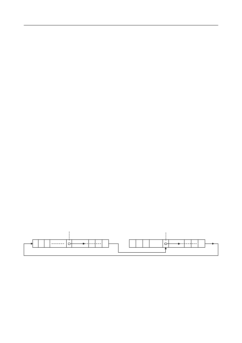
MSM54C865
° Semiconductor
38/44
SAM PORT OPERATION
Single Register Mode
High speed serial read or write operation can be performed through the SAM port independent
of the RAM port operation, except during read/write transfer cycles.
The preceding transfer operation determines the direction of data flow through the SAM port.
If the preceding transfer is a read transfer, the SAM port is in the output made. If the preceding
transfer is write or pseudo write transfer, the SAM port is in the input mode.
The pseudo write transfer only switches the SAM port from output mode to input mode (Data
is not transffered from SAM port to RAM port).
Serial data can be read out of the SAM after a read transfer has been performed. The data is
shifted out of the SAM starting at any of the 256 bits locations.
The TAP location corresponds to the column address selected at the falling edge of CAS during
the read or write transfer cycle. The SAM register is configured as a circular data register. The
data is shifted out sequentially starting from the selected TAP location to the most significant bit
(255) and then wraps around the least significant bit (0).
Split Register Mode
In split register mode, data can be shifted into or out of one half of the SAM while a split read
or split write transfer is being performed on the other half of the SAM.
Conventional (non split) read, write, or pseudo write transfer cycle must precede any split read
or split write transfers. The split read and write transfers will not change the SAM port mode set
by preceding conventional transfer operation. In the split register mode, serial data can be shifted
in or out of one of the split SAM registers starting from any at the 128 TAP locations, excluding
the last address of each split SAM. Data is shifted in or out sequentially starting from the selected
TAP location to the most significant bit (127 or 255) of the first split SAM. Then the SAM pointer
moves to the TAP location selected for the second split SAM to shift data in or out sequentially
starting from this TAP location to the most significant bit (255 or 127) and finally wraps around
to the least significant bit.
0 1 2
127
128
255
TAP
TAP
129
MSM54C865
° Semiconductor
39/44
DATA TRANSFER OPERATION
The MSM54C865 features two types of bidirectional data transfer capability between RAM and
SAM, as shown in Figure 1 below.
1) Conventional (non split) transfer : 256 words by 8 bits of data can be loaded from RAM to SAM
(Read transfer) or from SAM to RAM (write transfer).
2) Split transfer : 128 words by 8 bits of data can be loaded from the lower/upper half of the RAM
to the lower/upper half of the SAM (Split read transfer) or from the lower/upper half of SAM
to the lower/upper half of RAM (Split write transfer).
The conventional transfer and split transfer modes are controlled by the DSF input signal.
256 • 256 • 8
Memory
Array
256 • 8
256 • 128 • 8
Memory
Array
128 • 8
256 • 128 • 8
Memory
Array
128 • 8
1) Conventional Transfer
2) Split Transfer
Figure 1.
The MSM54C865 supports five types of transfer operation : Read transfer, Split read transfer,
Write transfer, Pseudo write transfer and Split write transfer as shown in truth table. Data
transfer is invoked by holding the DT/OE signal "low" at the falling edge of RAS. The type of
transfer operation is determined by the state of CAS, WB/WE, SE and DSF latched at the falling
edge of RAS. During conventional transfer operations, the SAM port is switched from input to
output mode (Read transfer) or output to input mode (Write/Pseudo write transfer) whereas it
remains unchanged during split transfer operation (Split read transfer or Split write transfer).

MSM54C865
° Semiconductor
40/44
Read Transfer Operation
Read transfer consists of loading a selected row of data from the RAM into the SAM register.
A read transfer is invoked by holding CAS "high" , DT/OE "low", WB/WE "high", and DSF "low"
at the falling edge of RAS. The low address selected at the falling edge of RAS determines the
RAM row to be transferred into the SAM. The transfer cycle is completed at the rising edge of DT/
OE. When the transfer is completed, the SAM port is set into the output mode. In a read/real time
read transfer cycle, the transfer of a new row of data is completed at the rising edge of DT/OE
and this data becomes valid on the SIO lines after the specified access time t
SCA
from the rising
edge of the subsequent SC cycles. The start address of the serial pointer of the SAM is determined
by the column address selected at the falling edge of CAS. In a read transfer cycle (which is
preceded by a write transfer cycle), SC clock must be held at a constant V
IL
or V
IH
, after the SC
high time has been satisfied. A rising edge of the SC clock must not occur until after the specified
delay t
TSD
from the rising edge of DT/OE.
In a real time transfer cycle ( which is preceded by another read transfer cycle), the previous
row data appears on the SIO lines until the DT/OE signal goes "high" and the serial access time
t
SCA
for the following serial clock is satisfied. This feature allows for the first bit of the new row
of data to appear on the serial output as soon as the last bit of the previous row has been strobed
without any timing loss. To make this continuous data flow possible, the rising edge of DT/OE
must be synchronized with RAS, CAS and the subsequent rising edge of SC (t
RTH
, t
CTH
, and t
TSL
/
t
TSD
must be satisfied).
Write Transfer Operation
Write transfer cycle consists of loading the content of the SAM register into a selected row of
the RAM. If the SAM data to be transferred must first be loaded through the SAM, a pseudo write
transfer operation must precede the write transfer cycles. A write transfer is invoked by holding
CAS "high", DT/OE "low", WB/WE "low", SE "low" and DSF "low" at the falling edge of RAS. This
write transfer is selectively controlled per RAM I/O block by setting the mask data on the Wi/
Oi lines at the falling edge of RAS. The row address selected at the falling edge of RAS determines
the RAM row address into which the data will be transferred. The column address selected at the
falling edge of CAS determines the start address of the serial pointer of the SAM. After the write
transfer is completed, the SIO lines are set in the input mode so that serial data synchronized with
the SC clock can be loaded. When consecutive write transfer operations are performed, new data
must not be written into the serial register until the RAS cycle of the preceding write transfer is
completed. Consequently, the SC clock must be held at a constant V
IL
or V
IH
during the RAS
cycle. A rising edge of the SC clock is only allowed after the specified delay t
SRD
from the rising
edge of RAS, at which time a new row of data can be written in the serial register.
Pseudo Write Transfer Operation
Pseudo write transfer cycle must be performed before loading data into the serial register after
a read transfer operation has been executed. The only purpose of a pseudo write transfer is to
change SAM port mode from output mode to input mode (A data transfer from SAM to RAM
does not occur). After the serial register is loaded with new data, a write transfer is invoked by
holding CAS "high", DT/OE "low", WB/WE "low", SE "high" and DSF "low" at the falling edge
of RAS. The timing conditions are the same as the one for the write transfer cycle except for the
state of SE at the falling edge of RAS.

MSM54C865
° Semiconductor
41/44
Split Data Transfer and QSF
The MSM54C865 features a bidirectional split data transfer capability between the RAM and
SAM. During split data transfer operation, the serial register is split into two halves which can
be controlled independently. Split read or split write transfer operation can be performed to or
from one half of the serial register while serial data can be shifted into or out of the other half of
the serial register. The most significant column address location (A7C) is controlled internally to
determine which half of the serial register will be reloaded from the RAM. QSF is an output which
indicates which half of the serial register is in an active state. QSF changes state when the last SC
clock is applied to active split SAM.
Split Read Transfer Operation
Split read transfer consists of loading 128 words by 8 bits of data from a selected row of the split
RAM into the corresponding non-active split SAM register. Serial data can be shifted out from
of the other half of the split SAM register simultaneously. During split read transfer operation,
the RAM port input clocks do not have to be synchronized with the serial clock SC, thus
eliminating timing restrictions as in the case of real time read transfers. A split read transfer can
be performed after a delay of t
STS
, from the change of state of the QSF output, is satisfied.
Conventional (non-split) read transfer operation must be preceded by split read transfer
cycles.
Split Write Transfer Operation
Split write transfer consists of loading 128 words by 8 bits of data from the non-active split SAM
register into a selected row of the corresponding split RAM. Serial data can be shifted into the
other half of the split SAM register simultaneously. During split write transfer operation, the
RAM port input clocks do not have to be synchronized with the serial clock SC, thus allowing
for real time transfer. A split write transfer can be performed after a delay of t
STS
, from the change
of state of the QSF output, is satisfied.
A pseudo write transfer operation must precede split write transfer. The purpose of the pseudo
write transfer operation is to switch the SAM port from output mode to input mode and to set
the initial TAP location prior to split write transfer operation.
Transfer Operation Without CAS
During all transfer cycles, the CAS input clock must be cycled, so that the column addresses
are latched at the falling edge of CAS, to set the SAM TAP location.
TAP Location in Split Transfer
1) In a split transfer operation, column address A0C through A6C must be latched at the falling
edge of CAS in order to set the TAP location in one of the split SAM registers. During a split
transfer, column address A7C is controlled internally and therefore it is ignored internally at the
falling edge of CAS. During a split transfer, it is not permissible to set the last address location
(A0C-A6C = 7F), in either the lower SAM or the upper SAM, as the TAP location.

MSM54C865
° Semiconductor
42/44
POWER-UP
Power must be applied to the RAS and DT/OE input signals to pull them "high" before or at
the same time as the V
CC
supply is turned on. After power-up, a pause of 200 ms minimum is
required with RAS and DT/OE held "high". After the pause, a minimum of 8 RAS and 8 SC
dummy cycles must be performed to stabilize the internal circuitry, before valid read, write or
transfer operations can begin. During the initialization period, the DT/OE signal must be held
"high". If the internal refresh counter is used, a minimum 8 CAS before RAS cycles are required
instead of 8 RAS cycles.
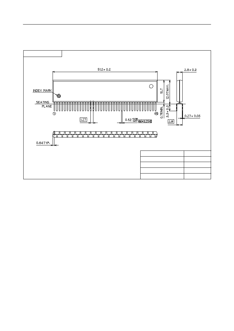
MSM54C865
° Semiconductor
43/44
(Unit : mm)
PACKAGE DIMENSIONS
ZIP40-P-475-1.27
Package material
Lead frame material
Pin treatment
Solder plate thickness
Package weight (g)
Epoxy resin
42 alloy
Solder plating
5 mm or more
3.46 TYP.
Mirror finish
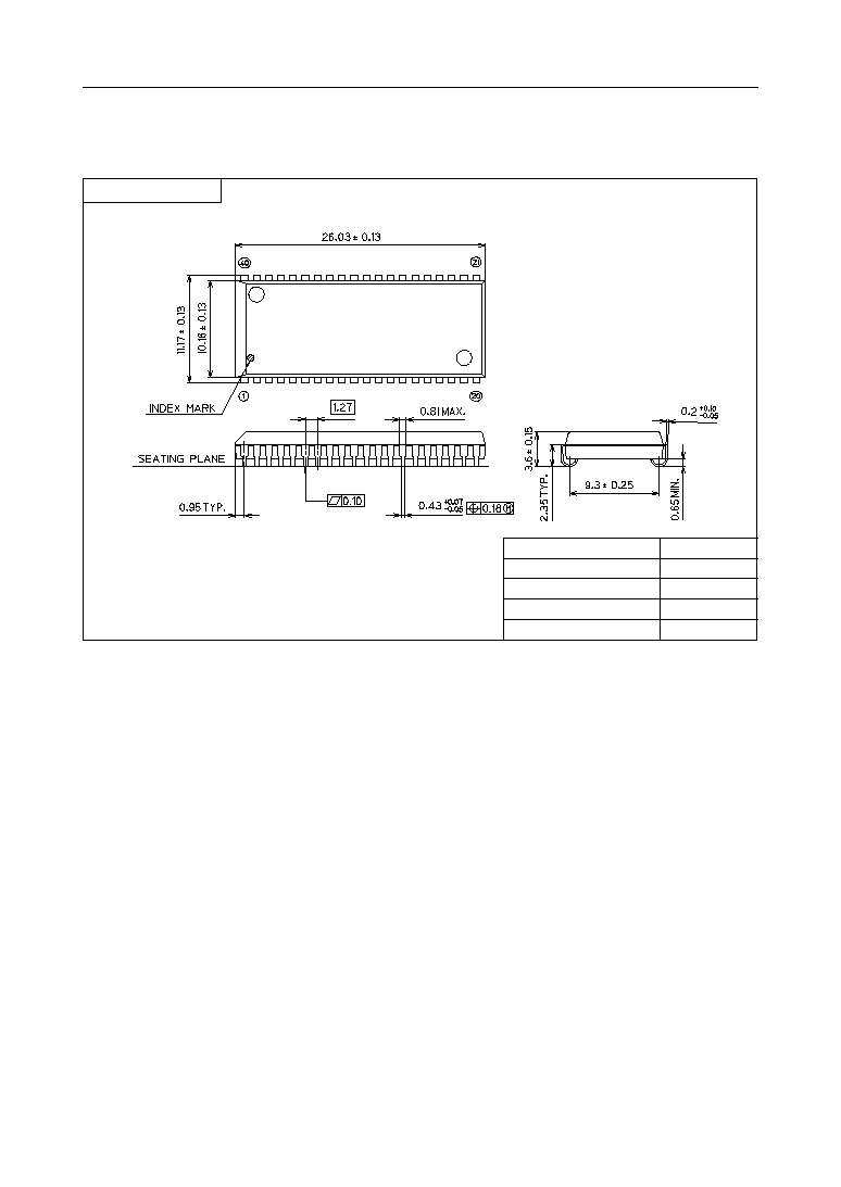
MSM54C865
° Semiconductor
44/44
(Unit : mm)
Notes for Mounting the Surface Mount Type Package
The SOP, QFP, TSOP, SOJ, QFJ (PLCC), SHP and BGA are surface mount type packages, which
are very susceptible to heat in reflow mounting and humidity absorbed in storage.
Therefore, before you perform reflow mounting, contact Oki's responsible sales person for the
product name, package name, pin number, package code and desired mounting conditions
(reflow method, temperature and times).
SOJ40-P-400-1.27
Package material
Lead frame material
Pin treatment
Solder plate thickness
Package weight (g)
Epoxy resin
42 alloy
Solder plating
5 mm or more
1.70 TYP.
Mirror finish