
1/66
° Semiconductor
MSM54V25632A
DESCRIPTION
The MSM54V25632A is a synchronous graphics random access memory organized as 128 K words
• 32 bits • 2 banks.
This device can operate up to 100 MHz by using synchronous interface. In addition, it has 8-column
Block Write function and Write per bit function which improves performance in graphics
systems.
FEATURES
∑ 131,072 words • 32 bits • 2 banks memory
∑ Single 3.3 V
±
0.3 V power supply
∑ LVTTL compatible inputs and outputs
∑ All input signals are latched at rising edge of system clock
∑ Auto precharge and controlled precharge
∑ Internal pipelined operation: column address can be changed every clock cycle
∑ Dual internal banks controlled by A9 (Bank Address: BA)
∑ Independent byte operation via DQM0 to DQM3
∑ 8-column Block Write function
∑ Persistent write per bit function
∑ Programmable burst sequence (Sequential/Interleave)
∑ Programmable burst length (1, 2, 4, 8 and full page)
∑ Programmable CAS latency (1, 2 and 3)
∑ Burst stop function (full-page burst)
∑ Power Down operation and Clock Suspend operation
∑ Auto refresh and self refresh capability
∑ 1,024 refresh cycles/16 ms
∑ Package:
100-pin plastic QFP
(QFP100-P-1420-0.65-BK4)
(Product : MSM54V25632A-xxAGBK4)
xx indicates speed rank.
PRODUCT FAMILY
° Semiconductor
MSM54V25632A
131,072-Word
• 32-Bit • 2-Bank Synchronous Graphics RAM
MSM54V25632A-10
Family
MSM54V25632A-12
100-pin Plastic QFP (14 • 20 mm)
100
Clock Frequency
MHz (Max.)
83
Package
E2L0068-19-61
This version: Jun. 1999
Previous version: Sep. 1998
2/66
° Semiconductor
MSM54V25632A
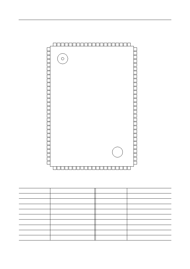
PIN CONFIGURATION (TOP VIEW)
DQ3
100-Pin Plastic QFP
1
V
CC
Q
2
DQ4
3
DQ5
4
V
SS
Q
5
DQ6
6
DQ7
7
V
CC
Q
8
DQ16
9
DQ17
10
V
SS
Q
11
DQ18
12
DQ19
13
V
CC
Q
14
V
CC
15
V
SS
16
DQ20
17
DQ21
18
V
SS
Q
19
DQ22
20
DQ23
21
V
CC
Q
22
DQM0
23
DQM2
24
WE
25
CAS
26
RAS
27
CS
28
BA (A9)
29
NC
30
DQ28
V
CC
Q
DQ27
DQ26
V
SS
Q
DQ25
DQ24
V
CC
Q
DQ15
DQ14
V
SS
Q
DQ13
DQ12
V
CC
Q
V
SS
V
CC
DQ11
DQ10
V
SS
Q
DQ9
DQ8
V
CC
Q
NC
DQM3
DQM1
CLK
CKE
DSF
NC
A8
80
79
78
77
76
75
74
73
72
71
70
69
68
67
66
65
64
63
62
61
60
59
58
57
56
55
54
53
52
51
A0
31
A1
32
A2
33
A3
34
V
CC
35
NC
36
NC
37
NC
38
NC
39
NC
40
NC
41
NC
42
NC
43
NC
44
NC
45
V
SS
46
A4
47
A5
48
A6
49
A7
50
DQ2
V
SS
Q
DQ1
DQ0
V
CC
NC
NC
NC
NC
NC
NC
NC
NC
NC
NC
V
SS
DQ31
DQ30
V
SS
Q
DQ29
100
99
98
97
96
95
94
93
92
91
90
89
88
87
86
85
84
83
82
81
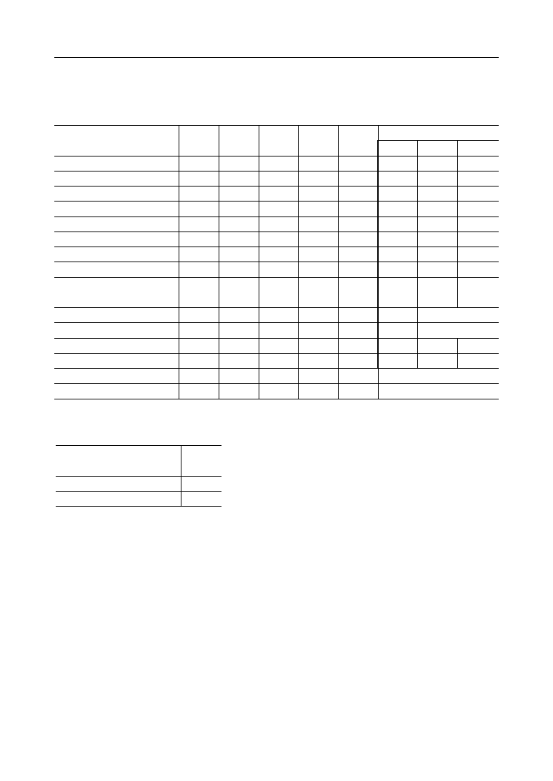
Pin Name
Function
Pin Name
Function
A0 - A9
Address Inputs
DQM0 - DQM3
DQ Mask Enable
A0 - A8
Row Address Inputs
DSF
Special Function Enable
A0 - A7
Column Address Inputs
CKE
Clock Enable
A9
Bank Address
CLK
System Clock Input
DQ0 - DQ31
Data Inputs/Outputs
V
CC
Supply Voltage
CS
Chip Select
V
SS
Ground
RAS
Row Address Strobe
V
CC
Q
Supply Voltage for DQ
CAS
Column Address Strobe
V
SS
Q
Ground for DQ
WE
Write Enable
NC
No Connection
Note:
The same power supply voltage must be provided to every V
CC
pin and V
CC
Q pin.
The same GND voltage level must be provided to every V
SS
pin and V
SS
Q pin.
3/66
° Semiconductor
MSM54V25632A
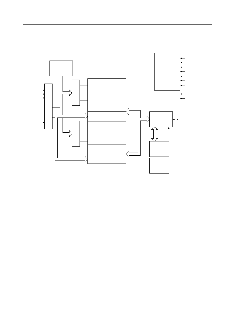
BLOCK DIAGRAM
A0
DQ0 to 31
DQM0 to 3
32
32
32
A1
A2
A9
Address Buffers
Column Decoders
Sense Amplifiers
4Mb
Memory Cells
Bank - A
Row Decoders
Column Decoders
Sense Amplifiers
4Mb
Memory Cells
Bank - B
Refresh
Counter
I/O Buffers
Color
Register
(32 bits)
Mask
Register
(32 bits)
Row Decoders
CLK
CKE
CS
RAS
CAS
WE
DSF
V
CC
V
SS
Timing
Generator
4/66
° Semiconductor
MSM54V25632A
PIN DESCRIPTION
*
Notes:
1. When CS is set "High" at a clock transition from "Low" to "High", all inputs except CLK, CKE, DQM0,
DQM1, DQM2, and DQM3 are invalid.
2. When issuing an active, read or write command, the bank is selected by A9.
3. The auto precharge function is enabled or disabled by the A8 input when the read or write command is
issued.
A9
0
1
Active, read or write
Bank A
Bank B
A8
0
Operation
After the end of burst, bank A holds the active status.
A9
0
0
0
After the end of burst, bank B holds the active status.
1
1
After the end of burst, bank A is precharged automatically.
After the end of burst, bank B is precharged automatically.
1
1
4. When issuing a precharge command, the bank to be precharged is selected by the A8 and A9 inputs.
A8
0
0
1
A9
0
1
X
Operation
Bank A is precharged.
Bank B is precharged.
Both banks A and B are precharged.
CLK
Fetches all inputs at the "H" edge.
CKE
Masks system clock to deactivate the subsequent CLK operation.
If CKE is deactivated, system clock will be masked so that the subsequent CLK operation is
deactivated. CKE should be asserted at least one cycle prior to a new command.
Row & column multiplexed.
Row address: RA0 ≠ RA8
Column address: CA0 ≠ CA7
RAS
CAS
WE
Functionality depends on the combination. For details, see the function truth table.
DQM0 -
DQM3
Masks the read data of two clocks later when DQM0 - DQM3 are set "H" at the "H" edge of the clock signal.
Masks the write data of the same clock when DQM0 - DQM3 are set "H" at the "H" edge of the clock signal.
Address
DQi
Data inputs/outputs are multiplexed on the same pin.
CS
Disables or enables device operation by asserting or deactivating all inputs except CLK, CKE,
DQM0, DQM1, DQM2 and DQM3.
Selects bank to be activated during row address latch time and selects bank for precharge and read/
write during column address latch time. A9 = "L" : Bank A, A9 = "H" : Bank B
BA (A9)
DSF
DSF is part of the inputs of graphics command of the MSM54V25632A.
If DSF is inactive (Low level), MSM54V25632A operates just like SDRAM.

5/66
° Semiconductor
MSM54V25632A
COMMAND OPERATION
Mode Register Set Command (CS, RAS, CAS, WE, DSF = "Low")
The MSM54V25632A has the mode register that defines the operation mode "CAS Latency,
Burst Length, Burst Sequence". The mode register is composed of ten bits of memories
corresponding to address inputs A0 - A8 and BA. The Mode Register Set command should be
executed just after the MSM54V25632A is powered on. Before entering this command, all banks
must be precharged. Next command can be issued after t
RSC
.
Special Mode Register Set Command (CS, RAS, CAS, WE = "Low", DSF = "High")
The MSM54V25632A has the 32-bit color register for block write operation and the 32-bit mask
register for write per bit operation. The Special Mode Register Set command performs loading
mask register or color register. When A5 is "high", The mask data presented on the DQ0 - DQ31
is latched into the mask register. When A6 is "high", The color data presented on the DQ0 - DQ31
is latched into the color register. The Special Mode Register Set command must be executed
before Masked Block Write and Write Per Bit operations. Next command can be issued after
t
RSC
.
Auto Refresh Command (CS, RAS, CAS, DSF = "Low", WE, CKE = "High")
The Auto Refresh command performs refresh automatically by the address counter. The refresh
operation must be performed 1024 times within 16 ms and the next command can be issued after
t
RC
from last Auto Refresh command. Before entering this command, all banks must be
precharged.
Self Refresh Entry/Exit Command (CS, RAS, CAS, DSF, CKE = "Low", WE = "High")
The self refresh operation continues after the Self Refresh Entry command is entered, with CKE
level left "low". This operation terminates by making CKE level "high". The self refresh
operation is performed automatically by the internal address counter on the MSM54V25632A
chip. In self refresh mode, no external refresh control is required. Before entering self refresh
mode, all banks must be precharged. Next command can be issued after t
RC
.
Single Bank Precharge Command (CS, RAS, WE, DSF, A8 = "Low", CAS = "High")
The Single Bank Precharge command triggers bank precharge operation. Precharge bank is
selected by BA.
All Banks Precharge Command (CS, RAS, WE, DSF = "Low", CAS, A8 = "High")
The All Bank Precharge command triggers precharge of both bank A and bank B.

6/66
° Semiconductor
MSM54V25632A
Bank Active and Masked Write Disable Command (CS, RAS, DSF = "Low", CAS, WE =
"High")
The Bank Active command activates the bank selected by BA. The Bank Active command
corresponds to conventional DRAM's RAS falling operation. Row addresses "A0 - A8 and BA"
are strobed. After this command, the write command and block write command for that bank
works as the no write per bit operation.
Bank Active and Masked Write Enable Command (CS, RAS = "Low", CAS, WE, DSF =
"High")
The Bank Active command activates the bank selected by BA. The Bank Active command
corresponds to conventional DRAM's RAS falling operation. Row addresses "A0 - A8 and BA"
are strobed. After this command, the write command and block write command for that bank
works as the write per bit operation.
Write Command (CS, CAS, WE, DSF, A8 = "Low", RAS = "High")
The Write command is required to begin burst write operation. Then burst access initial bit
column address is strobed.
Write with Auto Precharge Command (CS, CAS, WE, DSF = "Low", RAS, A8 = "High")
The Write with Auto Precharge command is required to begin burst write operation with
automatic precharge after the burst write. Any command that interrupts this operation cannot
be issued.
Masked Block Write Command (CS, CAS, WE, A8 = "Low", RAS, DSF = "High")
The Masked Block Write command is required to begin block write operation with column
mask. The masked block write operation performs writing in the 8 memory cells selected by
column addresses "A3 - A7". In this operation, data in color register is written to memory cells
with the column mask functions. At the same time, this command can perform write per bit
operation. The block write operation is not bursted.
7/66
° Semiconductor
MSM54V25632A
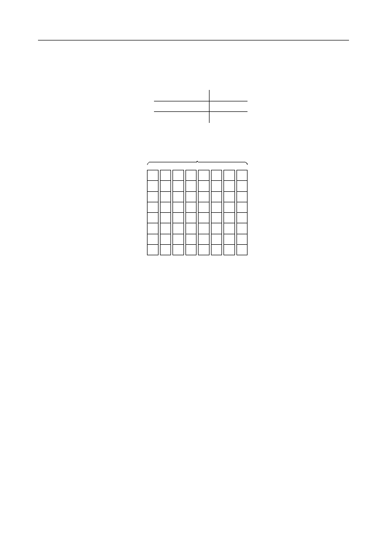
1
DQ0
8 Column • 8 DQ
Note : Location "*" can not be loaded.
Color Register
I/O Mask
Column Mask
11001110
11111010
10010011
1
*
*
1
*
*
1
1
1
*
*
1
*
*
1
0
0
*
*
0
*
*
0
0
0
*
*
0
*
*
0
1
1
*
*
1
*
*
1
*
*
*
*
*
*
*
*
1
1
*
*
1
*
*
1
*
*
*
*
*
*
*
*
Column 7
Column 6
Column 5
Column 4
Column 3
Column 2
Column 1
Column 0
DQ1
DQ2
DQ3
DQ4
DQ5
DQ6
DQ7
Remark: 1. This diagram shows only for DQ0 - 7. The other DQ is similar as this.
Column Mask
DQ0 - 7
: Column Mask for DQ0 - 7
DQ8 - 15 : Column Mask for DQ8 - 15
DQ16 - 23: Column Mask for DQ16 - 23
DQ24 - 31: Column Mask for DQ24 - 31
Write per Bit
Mask data = Mask Register + DQMi
DQMi is prior to data of Mask Register.
Block Write Function

8/66
° Semiconductor
MSM54V25632A
Masked Block Write with Auto Precharge Command (CS, CAS, WE = "Low", RAS, DSF,
A8 = "High")
The Masked Block Write with Auto Precharge command performs precharging at the bank
selected by BA automatically after Masked Block Write.
Read Command (CS, CAS, DSF, A8 = "Low", RAS, WE = "High")
The Read command is required to begin burst read operation. Then burst access initial bit
column address is strobed.
Read with Auto Prechaege Command (CS, CAS, DSF = "Low", RAS, WE, A8 = "High")
The Read with Auto Precharge command is required to begin burst read operation with auto
precharge after the burst read. Any command that interrupts this operation cannot be issued.
No Operation Command (CS, DSF = "Low", RAS, CAS, WE = "High")
The No Operation command does not trigger any operation.
Device Deselect Command (CS = "High")
The Device Deselect command disables the RAS, CAS, WE, DSF and Address input. This
command does not trigger any operation.
Data Write/Output Enable Command (DQMi = "Low")
The Data Write/Output Enable command enables DQ0 - DQ31 in read or write.
The each DQM0, 1, 2 and 3 corresponds to DQ0 - DQ7, DQ8 - DQ15, DQ16 - DQ23 and DQ24
- DQ31 respectively.
Data Mask/Output Disable Command (DQMi = "High")
The Data Mask/Output Disable command disables DQ0 - DQ31. In read cycle output buffers
are disabled after 2 clocks . In write cycle input buffers are disabled at the same clock. The each
DQM0, 1, 2 and 3 corresponds to DQ0 - DQ7, DQ8 - DQ15, DQ16 - DQ23 and DQ24 - DQ31
respectively.
Burst Stop Command (CS, WE, DSF = "Low", RAS, CAS = "High")
The Burst Stop command stops burst access when the access is in full page. After the Burst Stop
command is entered, the output buffer goes into high impedance state.
9/66
° Semiconductor
MSM54V25632A
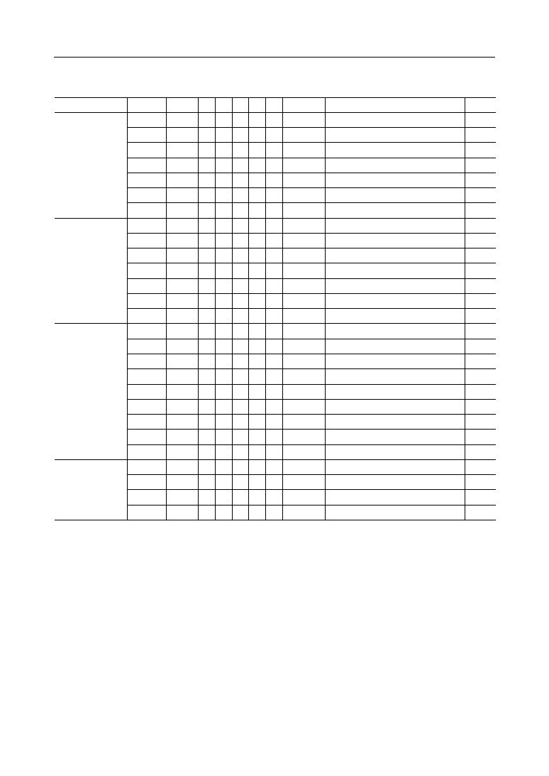
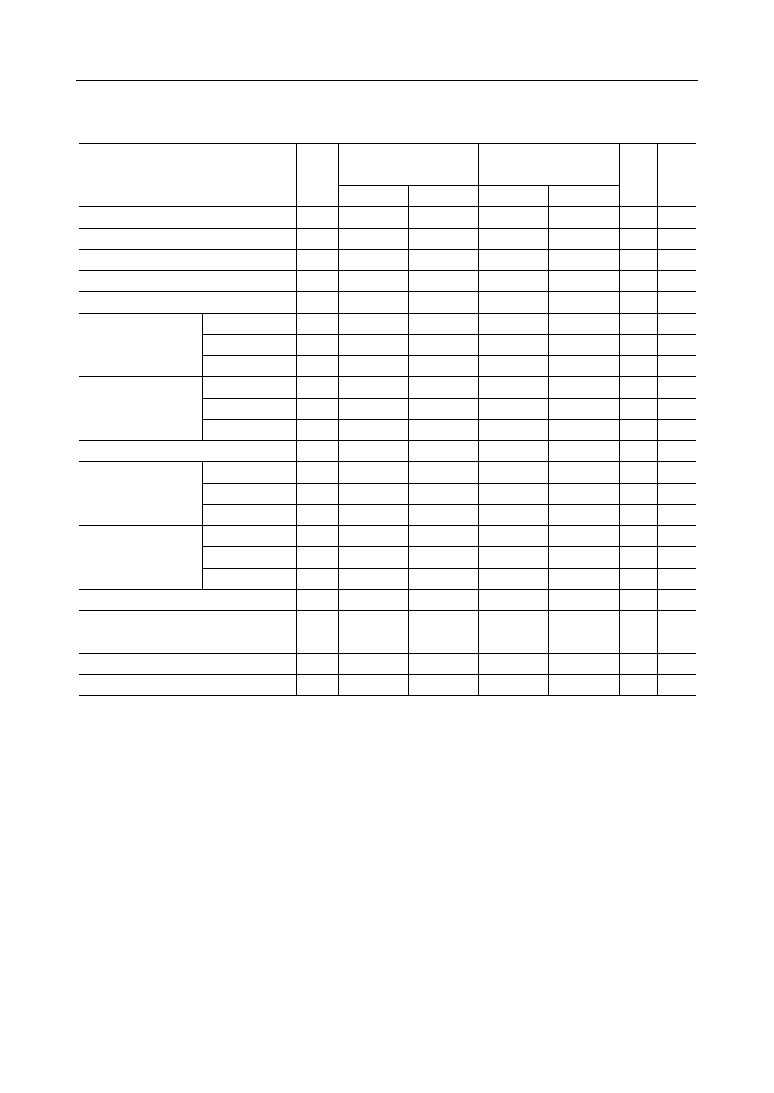
TRUTH TABLE
Command Truth Table
DQM Truth Table
Function
DQMi
Data Write/Output Enable
L
Data Mask/Output Disable
H
Function
CS
RAS
CAS
WE
DSF
Address
A9
A8
A7 - A0
Device Deselect
H
•
•
•
•
•
•
•
No Operation
L
H
H
H
L
•
•
•
Burst Stop in Full Page
L
H
H
L
L
•
•
•
Read
L
H
L
H
L
BA
L
CA
Read with Auto Precharge
L
H
L
H
L
BA
H
CA
Write
L
H
L
L
L
BA
L
CA
Write with Auto Precharge
L
H
L
L
L
BA
H
CA
Masked Block Write
L
H
L
L
H
BA
L
CA
Masked Block Write with Auto
Precharge
L
H
L
L
H
BA
H
CA
Bank Activate
L
L
H
H
L
BA
RA
Bank Activate with WPB Enable
L
L
H
H
H
BA
RA
Precharge Select Bank
L
L
H
L
L
BA
L
•
Precharge All Banks
L
L
H
L
L
•
H
•
Mode Register Set
L
L
L
L
L
OP. CODE
Special Register Set
L
L
L
L
H
OP. CODE
10/66
° Semiconductor
MSM54V25632A
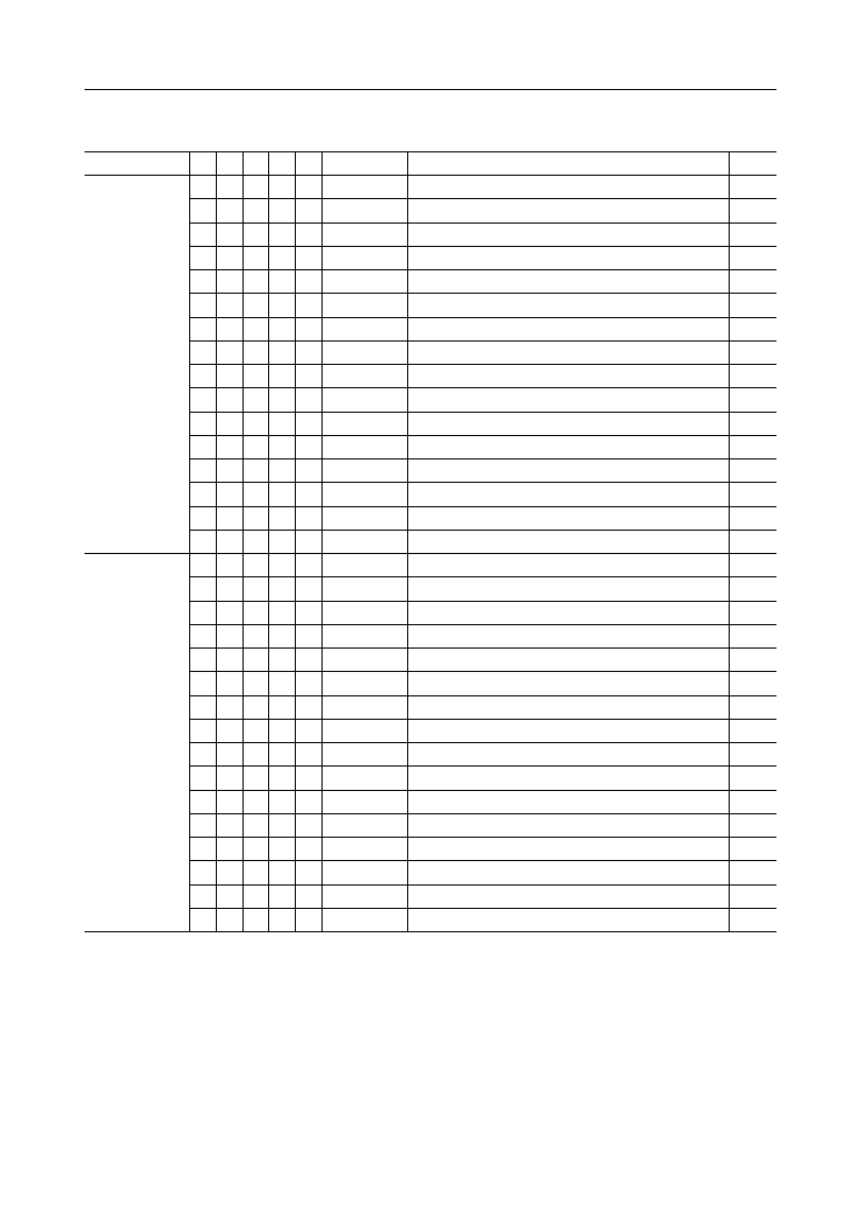
Function Truth Table (1/5)
Current State
CS RAS CAS WE DSF
Address
Note
Action
Idle
H
•
•
•
•
•
NOP or Power Down
L
H
H
H
•
•
NOP or Power Down
L
H
H
L
H
•
ILLEGAL
L
H
H
L
L
•
2
ILLEGAL
L
H
L
H
H
•
ILLEGAL
L
H
L
H
L
BA, CA, A8
2
ILLEGAL
L
H
L
L
H
BA, CA, A8
2
ILLEGAL
L
H
L
L
L
BA, CA, A8
2
ILLEGAL
L
L
H
H
H
BA, RA
Row Active with WPB
L
L
H
H
L
BA, RA
Row Active
L
L
H
L
H
•
ILLEGAL
L
L
H
L
L
BA, A8
3
NOP
L
L
L
H
H
•
ILLEGAL
L
L
L
H
L
•
4
Auto Refresh/Self refresh
L
L
L
L
H
Op-Code
Special Register Write
L
L
L
L
L
Op-Code
Mode Register Write
Row Active
(ACT)
H
•
•
•
•
•
NOP
L
H
H
H
•
•
NOP
L
H
H
L
H
•
ILLEGAL
L
H
H
L
L
•
2
ILLEGAL
L
H
L
H
H
•
ILLEGAL
L
H
L
H
L
BA, CA, A8
Read
L
H
L
L
H
BA, CA, A8
Block Write
L
H
L
L
L
BA, CA, A8
Write
L
L
H
H
H
BA, RA
2
ILLEGAL
L
L
H
H
L
BA, RA
2
ILLEGAL
L
L
H
L
H
•
ILLEGAL
L
L
H
L
L
BA, A8
Precharge
L
L
L
H
H
•
ILLEGAL
L
L
L
H
L
•
ILLEGAL
L
L
L
L
H
Op-Code
Special Register Write
L
L
L
L
L
Op-Code
ILLEGAL
Note 1
2
11/66
° Semiconductor
MSM54V25632A
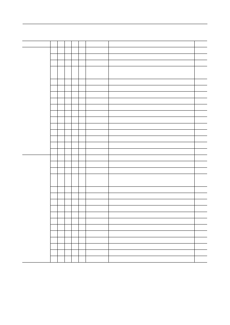
Current State
CS RAS CAS WE DSF
Address
Note
Action
Read
(RD)
H
•
•
•
•
•
NOP (Continue Row Active after Burst ends)
L
H
H
H
•
•
NOP (Continue Row Active after Burst ends)
L
H
H
L
H
•
ILLEGAL
L
H
H
L
L
•
1, 2, 4, 8 Burst Length; ILLEGAL
Full Page Burst; Burst Stop ∆ Bank Active
L
H
L
H
H
•
ILLEGAL
L
H
L
H
L
BA, CA, A8
Term Burst, new Read
L
H
L
L
H
BA, CA, A8
Term Burst, start Block Write
L
H
L
L
L
BA, CA, A8
Term Burst, start Write
L
L
H
H
H
BA, RA
ILLEGAL
L
L
H
H
L
BA, RA
ILLEGAL
L
L
H
L
H
•
ILLEGAL
L
L
H
L
L
BA, A8
Term Burst, execute Row Precharge
L
L
L
H
H
•
ILLEGAL
L
L
L
H
L
•
ILLEGAL
L
L
L
L
H
Op-Code
ILLEGAL
L
L
L
L
L
Op-Code
ILLEGAL
NOP (Continue Row Active after Burst ends)
NOP (Continue Row Active after Burst ends)
ILLEGAL
1, 2, 4, 8 Burst Length; ILLEGAL
Full Page Burst; Burst Stop ∆ Row Active
ILLEGAL
Term Burst, start Read
Term Burst, new Block Write
Term Burst, new Write
ILLEGAL
ILLEGAL
ILLEGAL
Term Burst, execute Row Precharge
ILLEGAL
ILLEGAL
ILLEGAL
ILLEGAL
Write/Block Write
(WT/BW)
H
•
•
•
•
•
L
H
H
H
•
•
L
H
H
L
H
•
L
H
H
L
L
•
L
H
L
H
H
•
L
H
L
H
L
BA, CA, A8
L
H
L
L
H
BA, CA, A8
L
H
L
L
L
BA, CA, A8
L
L
H
H
H
BA, RA
2
L
L
H
H
L
BA, RA
2
L
L
H
L
H
•
L
L
H
L
L
BA, A8
L
L
L
H
H
•
L
L
L
H
L
•
L
L
L
L
H
Op-Code
L
L
L
L
L
Op-Code
Note 1
2
2
Function Truth Table (2/5)

12/66
° Semiconductor
MSM54V25632A
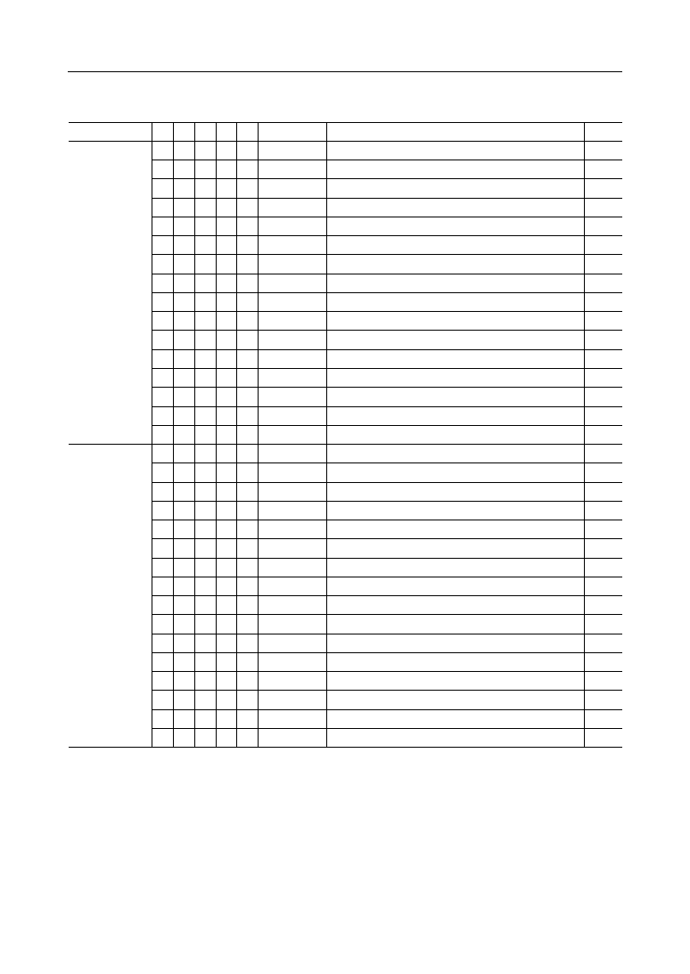
Current State
CS RAS CAS WE DSF
Address
Note
Action
Read with Auto
Precharge
(RAP)
H
•
•
•
•
•
L
H
H
H
•
•
L
H
H
L
H
•
L
H
H
L
L
•
L
H
L
H
H
•
L
H
L
H
L
BA, CA, A8
L
H
L
L
H
BA, CA, A8
L
H
L
L
L
BA, CA, A8
L
L
H
H
H
BA, RA
2
L
L
H
H
L
BA, RA
2
L
L
H
L
H
•
L
L
H
L
L
BA, A8
2
L
L
L
H
H
•
L
L
L
H
L
•
L
L
L
L
H
Op- Code
L
L
L
L
L
Op- Code
Note 1
NOP (Continue Burst to End and enter Row Precharge)
NOP (Continue Burst to End and enter Row Precharge)
ILLEGAL
ILLEGAL
ILLEGAL
ILLEGAL
ILLEGAL
ILLEGAL
ILLEGAL
ILLEGAL
ILLEGAL
ILLEGAL
ILLEGAL
ILLEGAL
ILLEGAL
ILLEGAL
Write/Block
Write with Auto
Precharge
(WAP/BWAP)
H
•
•
•
•
•
L
H
H
H
•
•
L
H
H
L
H
•
L
H
H
L
L
•
L
H
L
H
H
•
L
H
L
H
L
BA, CA, A8
L
H
L
L
H
BA, CA, A8
L
H
L
L
L
BA, CA, A8
L
L
H
H
H
BA, RA
2
L
L
H
H
L
BA, RA
2
L
L
H
L
H
•
L
L
H
L
L
BA, A8
2
L
L
L
H
H
•
L
L
L
H
L
•
L
L
L
L
H
Op- Code
L
L
L
L
L
Op- Code
NOP (Continue Burst to End and enter Row Precharge)
NOP (Continue Burst to End and enter Row Precharge)
ILLEGAL
ILLEGAL
ILLEGAL
ILLEGAL
ILLEGAL
ILLEGAL
ILLEGAL
ILLEGAL
ILLEGAL
ILLEGAL
ILLEGAL
ILLEGAL
ILLEGAL
ILLEGAL
Function Truth Table (3/5)
13/66
° Semiconductor
MSM54V25632A
Current State
CS RAS CAS WE DSF
Address
Note
Action
Precharging
(PRE)
H
•
•
•
•
•
2
2
2
2
2
2
3
NOP ∆ Idle after t
RP
L
H
H
H
•
•
NOP ∆ Idle after t
RP
L
H
H
L
H
•
ILLEGAL
L
H
H
L
L
•
ILLEGAL
L
H
L
H
H
•
ILLEGAL
L
H
L
H
L
BA, CA, A8
ILLEGAL
L
H
L
L
H
BA, CA, A8
ILLEGAL
L
H
L
L
L
BA, CA, A8
ILLEGAL
ILLEGAL
ILLEGAL
ILLEGAL
NOP ∆ Idle after t
RP
ILLEGAL
ILLEGAL
Special Register Write
ILLEGAL
L
L
H
H
H
BA, RA
L
L
H
H
L
BA, RA
L
L
H
L
H
•
L
L
H
L
L
BA, A8
L
L
L
H
H
•
L
L
L
H
L
•
L
L
L
L
H
Op-Code
L
L
L
L
L
Op-Code
Note 1
Refreshing
(REF)
H
•
•
•
•
•
NOP ∆ Idle after t
RC
L
H
H
H
•
•
NOP ∆ Idle after t
RC
L
H
H
L
H
•
ILLEGAL
L
H
H
L
L
•
ILLEGAL
L
H
L
H
H
•
ILLEGAL
ILLEGAL
ILLEGAL
ILLEGAL
L
H
L
H
L
BA, CA, A8
L
H
L
L
H
BA, CA, A8
L
H
L
L
L
BA, CA, A8
ILLEGAL
ILLEGAL
ILLEGAL
ILLEGAL
ILLEGAL
ILLEGAL
ILLEGAL
ILLEGAL
L
L
H
H
H
BA, RA
L
L
H
H
L
BA, RA
L
L
H
L
H
•
L
L
H
L
L
BA, A8
L
L
L
H
H
•
L
L
L
H
L
•
L
L
L
L
H
Op-Code
L
L
L
L
L
Op-Code
Function Truth Table (4/5)

14/66
° Semiconductor
MSM54V25632A
Current State
CS RAS CAS WE DSF
Address
Note
Action
NOP
NOP
ILLEGAL
ILLEGAL
ILLEGAL
ILLEGAL
ILLEGAL
ILLEGAL
ILLEGAL
ILLEGAL
ILLEGAL
ILLEGAL
ILLEGAL
ILLEGAL
ILLEGAL
ILLEGAL
Mode Register
Access
(MRA)
H
•
•
•
•
•
L
H
H
H
•
•
L
H
H
L
H
•
L
H
H
L
L
•
L
H
L
H
H
•
L
H
L
H
L
BA, CA, A8
L
H
L
L
H
BA, CA, A8
L
H
L
L
L
BA, CA, A8
L
L
H
H
H
BA, RA
L
L
H
H
L
BA, RA
L
L
H
L
H
•
L
L
H
L
L
BA, A8
L
L
L
H
H
•
L
L
L
H
L
•
L
L
L
L
H
Op-Code
L
L
L
L
L
Op-Code
Note 1
Special Mode
Register
Access
(SMRA)
H
•
•
•
•
•
NOP
L
H
H
H
•
•
NOP
L
H
H
L
H
•
ILLEGAL
L
H
H
L
L
•
ILLEGAL
L
H
L
H
H
•
ILLEGAL
ILLEGAL
ILLEGAL
ILLEGAL
L
H
L
H
L
BA, CA, A8
L
H
L
L
H
BA, CA, A8
L
H
L
L
L
BA, CA, A8
ILLEGAL
ILLEGAL
ILLEGAL
ILLEGAL
ILLEGAL
ILLEGAL
ILLEGAL
ILLEGAL
L
L
H
H
H
BA, RA
L
L
H
H
L
BA, RA
L
L
H
L
H
•
L
L
H
L
L
BA, A8
L
L
L
H
H
•
L
L
L
H
L
•
L
L
L
L
H
Op-Code
L
L
L
L
L
Op-Code
Function Truth Table (5/5)
Notes:
1. All inputs are enabled when CKE is set high for at least 1 cycle prior to the inputs.
2. Illegal to bank in specified state, but may be legal in some cases depending on the state of bank
selection.
3. NOP to bank precharging or in idle state. Precharges activated bank by BA or A8.
4. Illegal if any bank is not idle.
ABBREVIATIONS
RA = Row Address
BA = Bank Address
NOP = No OPeration command
CA = Column Address
AP = Auto Precharge
• = High or Low level (Don't care)
15/66
° Semiconductor
MSM54V25632A
Function Truth Table for CKE
Current State
(n) CKEn-1
Address
H
•
•
•
•
•
L
H
•
•
•
•
L
L
H
H
H
•
L
L
H
H
L
•
L
L
H
L
•
•
L
L
L
•
•
•
L
•
•
•
•
•
H
•
•
•
•
•
L
H
•
•
•
•
L
L
H
H
H
•
L
L
H
H
L
•
L
L
H
L
•
•
L
L
L
•
•
•
L
•
•
•
•
•
H
•
•
•
•
•
H
H
•
•
•
•
H
L
H
H
H
•
H
L
H
H
L
•
H
L
H
L
•
•
H
L
L
H
L
•
H
L
L
L
H
•
H
•
•
•
•
•
H
•
•
•
•
•
L
•
•
•
•
•
L
•
•
•
•
•
Self Refresh
(SREF)
Power Down
(PD)
All Banks Idle
Any State Other
Action
INVALID
Exit Self Refresh ∆ ABI
Exit Self Refresh ∆ ABI
ILLEGAL
ILLEGAL
ILLEGAL
NOP (Maintain Self Refresh)
INVALID
Exit Power Down ∆ ABI
Exit Power Down ∆ ABI
ILLEGAL
ILLEGAL
ILLEGAL
NOP (Continue power down mode)
Refer to Table
Enter Power Down
Enter Power Down
ILLEGAL
ILLEGAL
ILLEGAL
Enter Self Refresh
Refer to Operations in Table
Begin Clock Suspend Next Cycle
Enable Clock of Next Cycle
Continue Clock Suspension
CKEn
•
H
H
H
H
H
L
•
H
H
H
H
H
L
H
L
L
L
L
L
L
H
L
H
L
(ABI)
than Listed Above
H
L
L
L
L
•
ILLEGAL
L
L
•
•
•
•
•
NOP
L
•
•
•
•
•
•
•
•
•
•
•
•
•
•
•
•
•
•
•
•
L
•
•
•
•
•
•
Note
5
5
5
5
5
5
5
5
5
5
5
5
5
5
6
6
6
6
6
6
6
6
6
CS RAS CAS WE DSF
Notes:
5. If the minimum set-up time t
PDE
is satisfied when CKE transitions from "L" to "H", CKE
operates asynchronously so that a command can be input in the same internal clock cycle.
6. Power-down and self refresh can be entered only when all the banks are in an idle state.
16/66
° Semiconductor
MSM54V25632A
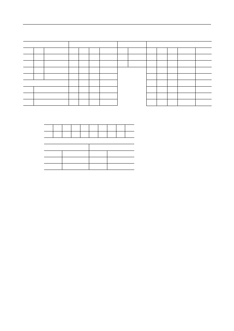
Mode Set Address Keys
Special Mode Set Address Keys
A6
A5
A4
CL
A3
BT
A2
A1
A0
BT = 0
BT = 1
CAS Latency (CL)
Burst Type (BT)
Burst Length (BL)
TM
A7
A8
Mode Setting
0
0
Reserved
1
0
Reserved
0
1
Burst
0
Single Bit
1
Length
A9
Operation Code
Write Burst Length
0
0
0
Reserved
0
Sequential
0
0
0
1
1
0
0
1
1
Interleave
0
0
1
2
2
0
1
0
0
1
0
4
4
0
1
1
0
1
1
8
8
1
2
3
1
0
0
Reserved
1
0
0
Reserved Reserved
1
0
1
Reserved
1
0
1
Reserved Reserved
1
1
0
Reserved
1
1
0
Reserved Reserved
1
1
1
Reserved
1
1
1
Full Page Reserved
Reserved
1
1
Note :
If LC and LM are both high (1), data of Mask and Color register will be unknown.
POWER ON SEQUENCE
1. With CKE = "H", DQM = "H" and the other inputs in NOP state, turn on the power
supply and start the system clock.
2. After the V
CC
voltage has reached the specified level, pause for 200 ms or more with
the input kept in NOP state.
3. Issue the precharge all bank command.
4. Apply an Auto-refresh eight or more times.
5. Enter the mode register setting command.
0
A9
0
A8
0
A7
LC
A6
LM
A5
0
A4
0
A3
0
A2
0
A1
0
A0
A6
Load Color (LC)
Function
A5
Load Mask (LM)
Function
Disable
Disable
Enable
Enable
0
0
1
1
17/66
° Semiconductor
MSM54V25632A
Burst Length and Sequence
BL = 2
Starting Address
Sequential Type
Interleave Type
(column address A0, binary)
0
0, 1
Not supported
1
1, 0
Not supported
BL = 4
Starting Address
Sequential Type
Interleave Type
(column address A1 - A0, binary)
00
0, 1, 2, 3
0, 1, 2, 3
01
1, 2, 3, 0
1, 0, 3, 2
10
2, 3, 0, 1
2, 3, 0, 1
11
3, 0, 1, 2
3, 2, 1, 0
BL = 8
Starting Address
Sequential Type
Interleave Type
(column address A2 - A0, binary)
000
0, 1, 2, 3, 4, 5, 6, 7
0, 1, 2, 3, 4, 5, 6, 7
001
1, 2, 3, 4, 5, 6, 7, 0
1, 0, 3, 2, 5, 4, 7, 6
010
2, 3, 4, 5, 6, 7, 0, 1
2, 3, 0, 1, 6, 7, 4, 5
011
3, 4, 5, 6, 7, 0, 1, 2
3, 2, 1, 0, 7, 6, 5, 4
100
4, 5, 6, 7, 0, 1, 2, 3
4, 5, 6, 7, 0, 1, 2, 3
101
5, 6, 7, 0, 1, 2, 3, 4
5, 4, 7, 6, 1, 0, 3, 2
110
6, 7, 0, 1, 2, 3, 4 ,5
6, 7, 4, 5, 2, 3, 0, 1
111
7, 0, 1, 2, 3, 4, 5, 6
7, 6, 5, 4, 3, 2, 1, 0
BL = Full : Sequential only
18/66
° Semiconductor
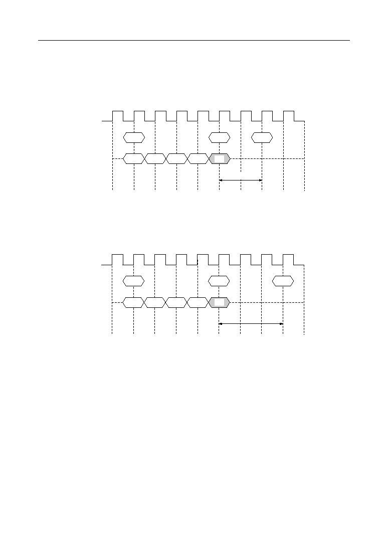
MSM54V25632A
PRECHARGE
Read Interrupted by Precharge
CL = 1
: At the same clock as the last read data.
CL = 2 or 3
: One clock earlier than the last read data.
0
1
2
3
4
5
6
7
8
BL = 4
(t
RAS
is satisfied)
Hi-Z
CLK
DQ
CL = 1
Q2
Q3
Q4
RD
PRE
Hi-Z
DQ
CL = 2
RD
PRE
DQ
CL = 3
RD
PRE
Hi-Z
Q1
Q2
Q3
Q4
Q1
Q2
Q3
Q4
Q1
19/66
° Semiconductor
MSM54V25632A
AUTO PRECHARGE
Read with Auto Precharge
0
1
2
3
4
5
6
7
8
BL = 4
(t
RAS
is satisfied)
Hi-Z
CLK
DQ
CL = 1
Q2
Q3
Q4
RAP
Hi-Z
DQ
CL = 2
RAP
DQ
CL = 3
RAP
Hi-Z
Auto precharge starts
Auto precharge starts
Auto precharge starts
Q1
Q2
Q3
Q4
Q1
Q2
Q3
Q4
Q1
20/66
° Semiconductor
MSM54V25632A
Write with Auto Precharge
0
1
2
3
4
5
6
7
8
BL = 4
(t
RAS
is satisfied)
Hi-Z
CLK
DQ
CL = 1
WAP
Hi-Z
DQ
CL = 2
WAP
DQ
CL = 3
WAP
Hi-Z
Auto precharge starts
Auto precharge starts
Auto precharge starts
D2
D3
D4
D1
D2
D3
D4
D1
D2
D3
D4
D1
Block Write with Auto Precharge
0
1
2
3
4
5
(t
RAS
is satisfied)
Hi-Z
CLK
DQ
CL = 1
BWAP
Hi-Z
DQ
CL = 2
DB
BWAP
DQ
CL = 3
BWAP
Hi-Z
Auto precharge starts
Auto precharge starts
Auto precharge starts
t
BWC
DB
DB
21/66
° Semiconductor
MSM54V25632A
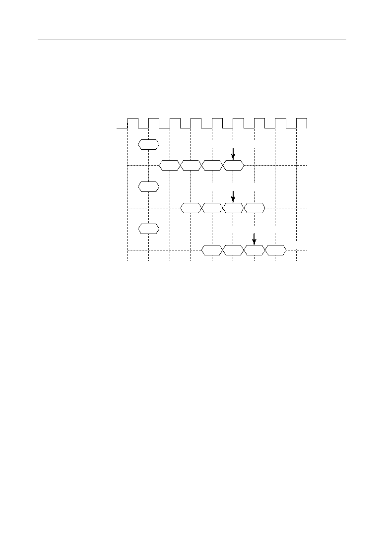
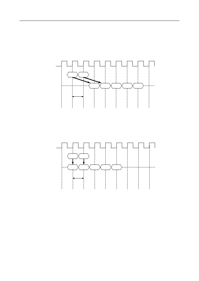
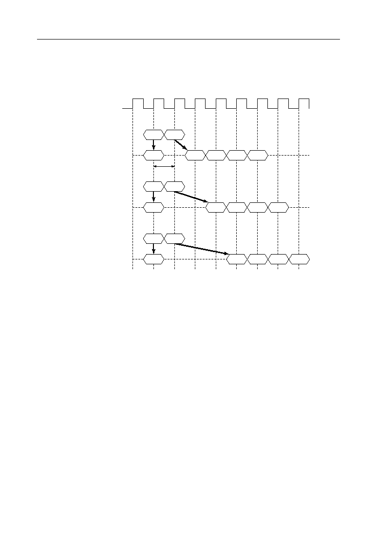
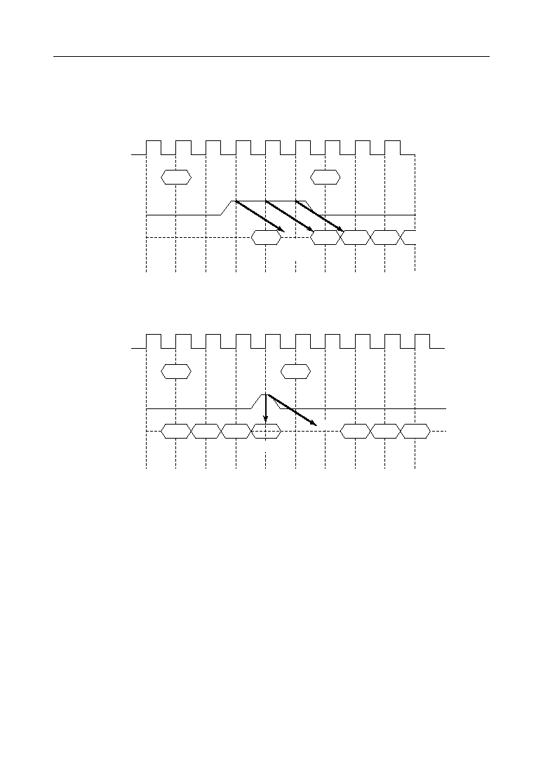
READ/WRITE COMMAND INTERVAL
Read to Read Command Interval
0
1
2
3
4
5
6
7
8
BL = 4, CL = 2
Hi-Z
CLK
DQ
QB1
QB2
QB3
QB4
RD-A
RD-B
QA1
1 cycle
Write to Write Command Interval
0
1
2
3
4
5
6
7
8
BL = 4, CL = 2
Hi-Z
CLK
DQ
DB1
DB2
DB3
DB4
WT-A
WT-B
DA1
1 cycle
22/66
° Semiconductor
MSM54V25632A
Write to Read Command Interval
0
1
2
3
4
5
6
7
8
BL = 4
Hi-Z
CLK
DQ
CL = 1
QB2
QB3
QB4
WT-A
RD-B
DQ
CL = 2
DQ
CL = 3
QB1
DA1
1 cycle
Hi-Z
QB2
QB3
QB4
WT-A
RD-B
QB1
DA1
Hi-Z
QB2
QB3
QB4
WT-A
RD-B
QB1
DA1

23/66
° Semiconductor
MSM54V25632A
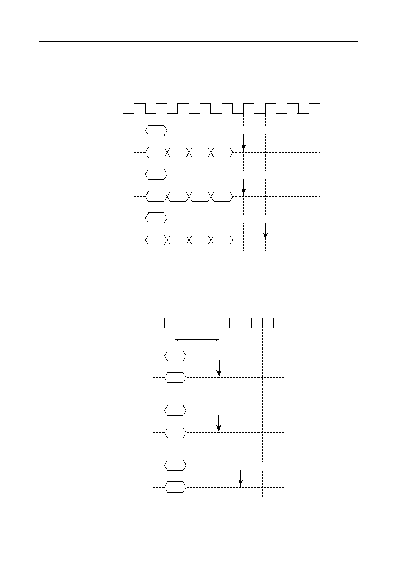
Block Write to Write/Block Write Command Interval
Block Write to Read Command Interval
0
1
2
3
4
5
6
7
8
Hi-Z
CLK
DQ
BW-A
DB
DA
BW-B
CL = 2
t
BWC
DQ
BW-A
DB1
DB2
DB3
DB4
DA
WT-B
BL = 4, CL = 2
t
BWC
0
1
2
3
4
5
6
7
8
Hi-Z
CLK
DQ
CL = 1
BW-A
DQ
CL = 2
DQ
CL = 3
QB2
QB3
QB4
QB1
DA
RD-B
t
BWC
Hi-Z
BW-A
QB2
QB3
QB4
QB1
DA
RD-B
t
BWC
Hi-Z
BW-A
QB2
QB3
QB4
QB1
DA
RD-B
t
BWC
24/66
° Semiconductor
MSM54V25632A
Read to Write/Block Write Command Interval
0
1
2
3
4
5
6
7
8
CL = 1, 2, 3
Hi-Z
CLK
DQM
RD-A
WT-B
DQ
DB2
DB3
DB4
DB1
1 cycle
BL = 8, CL = 1, 2
0
1
2
3
4
5
6
7
8
9
CLK
DQM
CL = 1
RD-A
WT-B
DQ
QA2
QA3
QA4
QA1
DB2
DB3
DB1
Hi-Z is
necessary
DQM
CL = 2
RD-A
WT-B
DQ
QA1
QA2
QA3
DB2
DB3
DB1
Hi-Z is
necessary
25/66
° Semiconductor
MSM54V25632A
0
1
2
3
4
5
6
7
8
ex.) CL = 3, BL = 4
CLK
DQM
RD-A
WT-B
DQ
QA1
DB2
DB3
DB1
Hi-Z is
necessary
ex.) CL = 1, BL = 4
CLK
DQM
WT-A
RD-B
DQ
DA1
QB2
QB3
Hi-Z
DA2
DA3
|
0
1
2
3
4
5
6
7
8
9
QB4
Note
Note : DQM can mask both data-in and data-out in this special case.
26/66
° Semiconductor
MSM54V25632A
BURST TERMINATION
Burst Stop Command in Full Page
0
1
2
3
4
5
6
7
8
BL = Full Page, CL = 1, 2, 3
Hi-Z
CLK
D2
D3
D4
WT
BST
CL = 1, 2, 3
DQ
D1
0
1
2
3
4
5
6
7
8
BL = Full Page, CL = 1, 2, 3
Hi-Z
CLK
Q2
Q3
RD
BST
CL = 1
DQ
Q1
Hi-Z
Q2
Q3
CL = 2
DQ
Q1
Hi-Z
Q2
Q3
CL = 3
DQ
Q1
27/66
° Semiconductor
MSM54V25632A
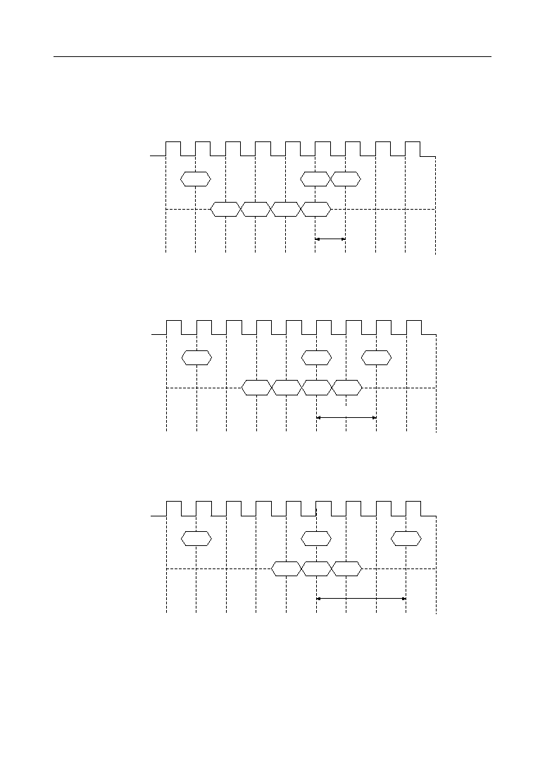
Precharge Termination in READ Cycle
0
1
2
3
4
5
6
7
8
BL = X, CL = 1
CLK
RD
PRE
ACT
DQ
Q1
Q3
Q4
Q2
Hi-Z
t
RP
0
1
2
3
4
5
6
7
8
BL = X, CL = 2
CLK
RD
PRE
ACT
DQ
Q1
Q3
Q4
Q2
Hi-Z
t
RP
0
1
2
3
4
5
6
7
8
BL = X, CL = 3
CLK
RD
PRE
ACT
DQ
Q1
Q3
Q2
Hi-Z
t
RP
28/66
° Semiconductor
MSM54V25632A
Precharge Termination in WRITE Cycle
0
1
2
3
4
5
6
7
8
BL = X, CL = 1, 2
CLK
WT
PRE
ACT
DQ
D3
D2
D1
D4
Hi-Z
t
RP
D5
Note : D5 data will not be written
0
1
2
3
4
5
6
7
8
BL = X, CL = 3
CLK
WT
PRE
ACT
DQ
D3
D2
D1
Hi-Z
t
RP
D4
D5
Note : D5 data will not be written

29/66
° Semiconductor
MSM54V25632A
ELECTRICAL CHARACTERISTICS
Note :
All voltages are referenced to V
SS
.
Absolute Maximum Ratings
Parameter
Unit
Symbol
Voltage on Power Supply Pin
Relative to GND
V
CC
, V
CC
Q
V
Voltage on Input Pin Relative to GND
V
T
V
Short Circuit Output Current
I
OS
mA
Power Dissipation
P
D
W
Storage Temperature
T
stg
∞C
Condition
--
--
--
Ta = 25∞C
--
Rating
≠1.0 to 4.6
≠1.0 to V
CC
+ 0.5 £ 4.6
50
1
Operating Temperature
T
opr
∞C
--
0 to 70
≠55 to 150
Caution:
Exposing the device to stress above those listed in Absolute Maximum Ratings could
cause permanent damage. The device is not meant to be operated under conditions
outside the limits described in the operational section of this specification. Exposure to
Absolute Maximum Rating conditions for extended periods may affect device reliability.
Recommended Operating Conditions
Parameter
Min.
Symbol
Power Supply Voltage
V
CC
3.0
Input High Voltage
V
IH
2.0
Input Low Voltage
V
IL
≠0.3
Typ.
3.3
--
--
Max.
3.6
V
CC
+ 0.3
0.8
Unit
V
V
V
(Ta = 0∞C to 70∞C)
Capacitance
Parameter
Min.
Symbol
Input Capacitance
(CLK, CKE, CS, RAS, CAS, WE, DSF, DQM)
C
I1
--
C
I2
--
Input/Output Capacitance
(DQ0 - DQ31)
C
I/O
--
Max.
6
6
7
Unit
pF
pF
pF
(V
CC
= 3.3 V ±0.3 V, Ta = 25∞C, f = 1 MHz)
Input Capacitance (A0 - A9)
DC Characteristics 1
Parameter
Symbol
Test Condition
I
OH
= ≠2 mA
Output High Voltage
V
OH
Unit
V
Max.
--
Min.
2.4
I
OL
= 2 mA
Output Low Voltage
V
OL
V
0.4
--
0 V £ V
I
£ 3.6 V;
All other pins not under test = 0 V
Input Leakage Current
I
LI
mA
10
≠10
D
OUT
is disabled, 0 V £ V
O
£ 3.6 V
Output Leakage Current
I
LO
mA
10
≠10
30/66
° Semiconductor
MSM54V25632A
DC Characteristics 2
Notes 1.
I
CC1
depends on output loading and cycle rates. Specified values are obtained with the
output open. In addition to this, I
CC1
is measured on condition that addresses are
changed only one time during t
CK (MIN.)
.
2.
I
CC4
depends on output loading and cycle rates. Specified values are obtained with the
output open. In addition to this, I
CC4
is measured on condition that addresses are
changed only one time during t
CK (MIN.)
.
3.
I
CC5
is measured on condition that addresses are changed only one time during t
CK
(MIN.)
.
Parameter
Symbol
Test Condition
Burst length = 1, t
RAS
t
RAS (MIN.)
,
t
RP
t
RP (MIN.)
,
I
O
= 0 mA
Operating Current
I
CC1
Unit
Max.
Note
155
175
mA
1
CKE £ V
IL (MAX.),
t
CK
= 15 ns
Precharge Standby Current I
CC2
P
mA
4
CKE £ V
IL (MAX.)
, t
CK
= ∑
in Power Down Mode
I
CC2
PS
3
CKE V
IH (MIN.)
, t
CK
= 15 ns,
Precharge Standby Current
CS V
IH (MIN.)
,
in Non Power Down Mode
I
CC2
N
60
Input signals are changed one time during 30 ns.
mA
CKE V
IH (MIN.)
, t
CK
= ∑,
I
CC2
NS
30
Input signals are stable.
CKE £ V
IL (MAX.)
, t
CK
= 15 ns
Active Standby Current
I
CC3
P
mA
4
CKE £ V
IL (MAX.)
, t
CK
= ∑
in Power Down Mode
I
CC3
PS
3
CKE V
IH (MIN.)
, t
CK
= 15 ns,
Active Standby Current
CS V
IH (MIN.)
,
in Non Power Down Mode
I
CC3
N
70
Input signals are changed one time during 30 ns.
mA
CKE V
IH (MIN.)
, t
CK
= ∑,
I
CC3
NS
35
Input signals are stable.
t
CK
t
CK (MIN.)
,
Operating Current
I
CC4
120
130
I
O
= 0 mA
(Burst Mode)
180
240
170
mA
2
230
t
RC
t
RC (MIN.)
Refresh Current
I
CC5
CKE £ 0.2 V
Self Refresh Current
I
CC6
mA
3
t
CK
t
CK (MIN.)
, I
O
= 0 mA,
Operating Current
CAS cycle = 20 ns
(Block Write Mode)
I
CC7
mA
240
CAS Latency = 1
CAS Latency = 2
CAS Latency = 3
-12
-10
4
3
60
30
4
3
70
35
3
240
165
145
mA
3
Max.
31/66
° Semiconductor
MSM54V25632A
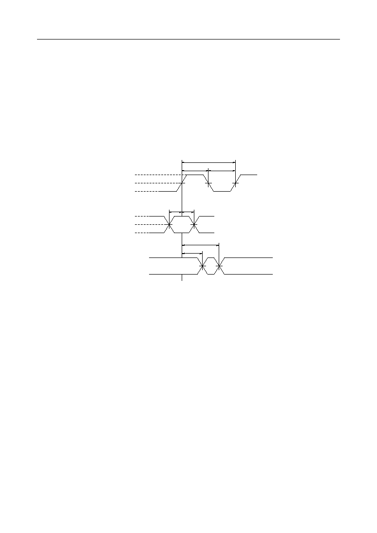
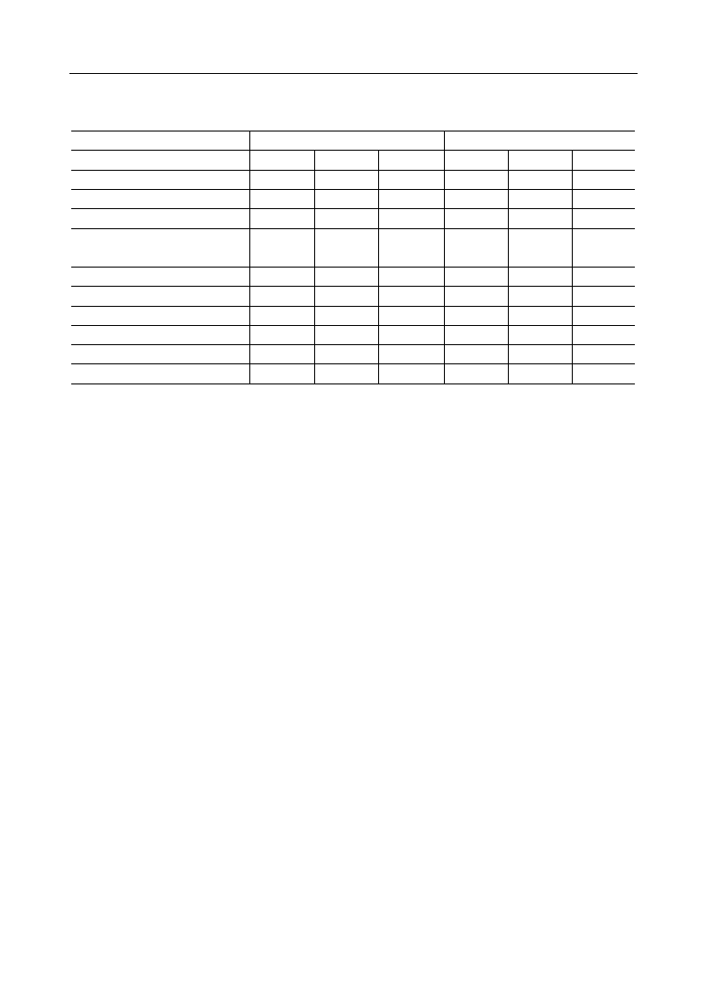
AC Characteristics
Test conditions
∑ AC measurements assume t
T
= 1 ns.
∑ Reference level for measuring timing of input signals is 1.4 V. Transition times are measured
between V
IH
and V
IL
.
∑ If t
T
is longer than 1 ns, reference level for measuring timing of input signals is V
IH (MIN.)
and V
IL
(MAX)
.
∑ An access time is measured at 1.4 V.
2.8 V
t
CK
1.4 V
CLK
V
SS
2.8 V
1.4 V
Input
V
SS
t
CH
t
CL
t
Setup
t
Hold
Output
1.4 V
1.4 V
t
OH
t
AC
32/66
° Semiconductor
MSM54V25632A
Synchronous Characteristics
Parameter
Unit Note
MSM54V25632A
-10
CAS Latency = 3 t
CK3
Min.
10
Max.
(100 MHz)
ns
Symbol
Min.
12
Max.
(83 MHz)
Clock Cycle Time
CAS Latency = 2 t
CK2
15
(66 MHz)
ns
18
(55 MHz)
CAS Latency = 1 t
CK1
30
(33 MHz)
ns
36
(28 MHz)
CAS Latency = 3 t
AC3
--
9
ns
1
--
10
Access Time from CLK CAS Latency = 2 t
AC2
--
13
ns
1
--
15
CAS Latency = 1 t
AC1
--
27
ns
1
--
32
--
--
--
--
8
12
26
--
--
--
--
--
--
CLK High Level Width
t
CH
3.5
--
ns
4
CLK Low Level Width
t
CL
3.5
--
ns
4
Data-out Hold Time
t
OH
3
--
ns
3
Data-out Low-impedance Time
t
LZ
0
--
ns
0
Data-out
CAS Latency = 3 t
HZ3
3
8
ns
3
High-impedance Time
CAS Latency = 2 t
HZ2
3
12
ns
3
CAS Latency = 1 t
HZ1
3
26
ns
3
Data-in Setup Time
t
DS
3
--
ns
3.5
Data-in Hold Time
t
DH
1
--
ns
1.5
Address Setup Time
t
AS
3
--
ns
3.5
Address Hold Time
t
AH
1
--
ns
1.5
CKE Setup Time
t
CKS
3
--
ns
3.5
CKE Hold Time
t
CKH
1
--
ns
1.5
MSM54V25632A
-12
t
CMS
3
--
ns
3.5
--
Command (CS, RAS, CAS, WE, DSF,
DQM) Setup Time
t
CMH
1
--
ns
1.5
--
Command (CS, RAS, CAS, WE, DSF,
DQM) Hold Time
Note
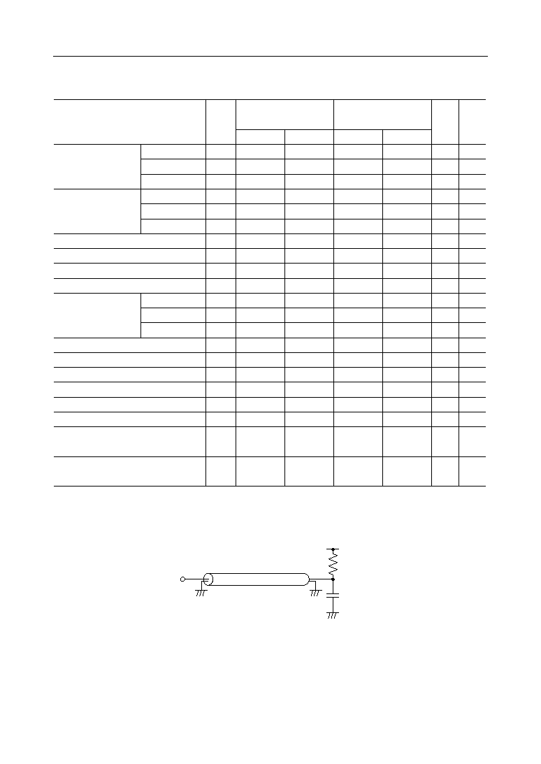
1.
Output load.
Output
Z = 50 W
30 pF
50 W
1.4 V
33/66
° Semiconductor
MSM54V25632A
Asynchronous Characteristics
MSM54V25632A
-12
Parameter
Unit Note
MSM54V25632A
-10
t
RC
Min.
90
Max.
ns
Symbol
Min.
108
REF to REF/ACT Command Period
t
RAS
60
120,000
ns
72
120,000
ACT to PRE Command Period
t
RP
30
ns
36
PRE to ACT Command Period
t
RCD
30
ns
36
Delay Time ACT to READ/WRITE Command
t
RRD
20
ns
24
ACT (0) to ACT (1) Command Period
CAS Latency = 3 t
DPL3
20
ns
24
Data-in to PRE
CAS Latency = 2 t
DPL2
20
ns
24
Command Period
CAS Latency = 1 t
DPL1
20
ns
24
CAS Latency = 3 t
DAL3
5
CLK
5
Data-in to ACT (REF)
CAS Latency = 2 t
DAL2
3
CLK
3
Command Period
CAS Latency = 1 t
DAL1
2
CLK
2
(Auto Precharge)
t
BWC
20
ns
24
Block Write Cycle Time
CAS Latency = 3 t
BPL3
30
ns
36
Block Write Data-in
CAS Latency = 2 t
BPL2
30
ns
36
to PRE Command
CAS Latency = 1 t
BPL1
30
ns
36
Period
CAS Latency = 3 t
BAL3
6
CLK
6
Block Write Data-in
Active (REF)
Command Period
(Auto Precharge)
CAS Latency = 2 t
BAL2
4
CLK
4
CAS Latency = 1 t
BAL1
2
CLK
2
t
RSC
20
ns
20
Mode Register Set Cycle Time
t
T
1
30
ns
1
30
Transition Time
t
REF
--
16
ms
16
Refresh Time
--
--
--
--
--
--
--
--
--
--
--
--
--
--
--
--
--
--
--
--
--
--
--
--
--
--
--
--
--
--
--
--
--
--
--
--
--
Max.
t
PDE
8
ns
10
CKE Setup Time
--
--
(Precharge Power Down Exit)
34/66
° Semiconductor
MSM54V25632A
TIMING WAVEFORM
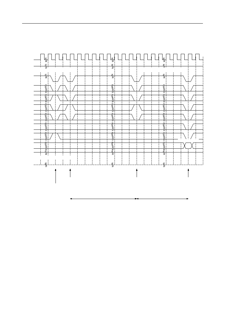
AC Parameters for Read Timing
(BL = 2, CL = 2)
CLK
0
CKE
CS
RAS
CAS
WE
A9
(BA)
A8
ADD
DQM
0 - 3
DQ
P
Q
,
y
|
~
Q
Hi-Z
t
CKH
t
CMS
t
CMH
t
CK
t
CH
t
CKS
t
CMS
t
CMH
t
CL
z
P
Q
z
~
~
P
Q
P
Q
z
P
Q
z
~
P
z
P
z
P
P
z
P
z
,
y
,
y
,
y
|
|
,
y
|
|
P
Q
Q
Q
~
Q
~
~
Q
z
P
Q
z
~
P
Q
P
Q
z
~
P
Q
,
y
z
P
,
y
z
|
P
z
z
P
P
|
|
|
,
y
,
y
t
AS
t
AH
DSF
Q
,
y
Q
,
y
|
~
|
~
Q
Q
,
y
Q
,
y
|
~
t
RC
t
RAS
t
RRD
t
RP
t
RCD
t
LZ
t
OH
t
OH
t
AC
t
AC
t
HZ
1
2
3
4
5
6
7
8
9
10
11
12
13
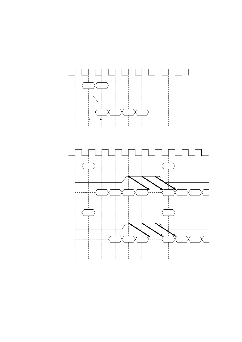
Auto Precharge
Start for Bank B
ACT-A
RD-A
ACT-B
RAP-B
PRE-A
ACT-A
35/66
° Semiconductor
MSM54V25632A
AC Parameters for Write Timing
(BL = 4, CL = 2)
CLK
CKE
CS
RAS
CAS
WE
A9
(BA)
A8
ADD
DQM
0 - 3
DQ
Hi-Z
0
DSF
t
CMS
t
CMH
t
AS
t
AH
t
CMS
t
CMH
t
DS
t
DH
t
RCD
t
RRD
t
DAL
t
DPL
t
RP
t
RC
t
CKH
Q
,
y
|
~
|
~
|
~
Q
z
P
Q
P
P
z
P
P
z
z
P
,
y
,
y
Q
|
|
|
,
y
|
,
y
|
P
P
P
Q
,
y
Q
|
~
Q
|
~
Q
z
P
Q
z
~
P
Q
~
~
Q
Q
Q
,
y
|
~
Q
|
~
,
y
Q
Q
Q
~
~
~
Q
~
Q
~
Q
Q
P
Q
z
~
~
P
Q
z
~
P
Q
~
P
Q
~
,
y
|
~
1
2
3
4
5
6
7
8
9
21
20
19
18
17
16
15
14
13
12
11
10
t
CKS
Auto Precharge
Start for Bank B
Auto Precharge
Start for Bank A
ACT-A
ACT-B
WAP-A
ACT-A
WAP-B
WAP-A
PRE-A
ACT-A
36/66
° Semiconductor
MSM54V25632A
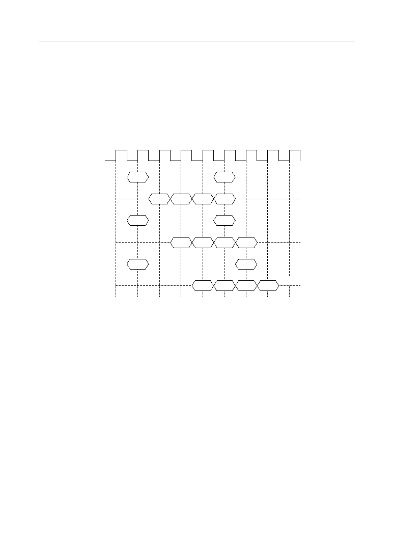
Relationship between Frequency and Latency
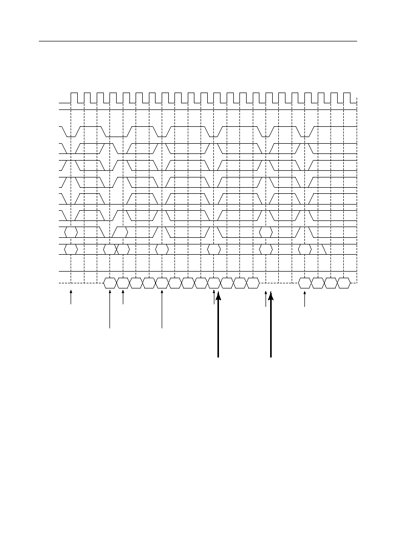
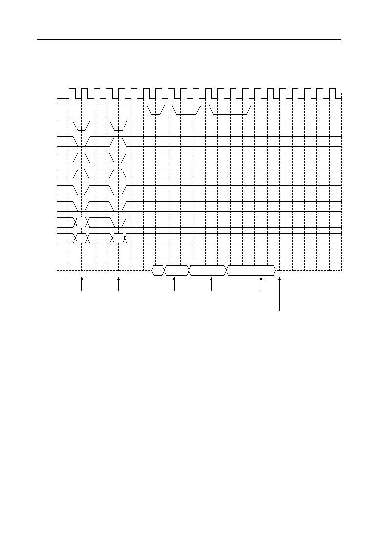
Rate
36
MSM54V25632A-12
18
12
30
MSM54V25632A-10
15
10
Clock Cycle Time [ns]
28
55
83
33
66
100
Frequency [MHz]
1
2
3
1
2
3
CAS Latency
1
2
3
1
2
3
[t
RCD
]
2
4
6
2
4
6
RAS Latency
(CAS Latency + [t
RCD
])
3
6
9
3
6
9
[t
RC
]
2
4
6
2
4
6
[t
RAS
]
1
2
2
1
2
2
[t
RRD
]
1
2
3
1
2
3
[t
RP
]
1
2
2
1
2
2
[t
DPL
]
2
3
5
2
3
5
[t
DAL
]
37/66
° Semiconductor
MSM54V25632A
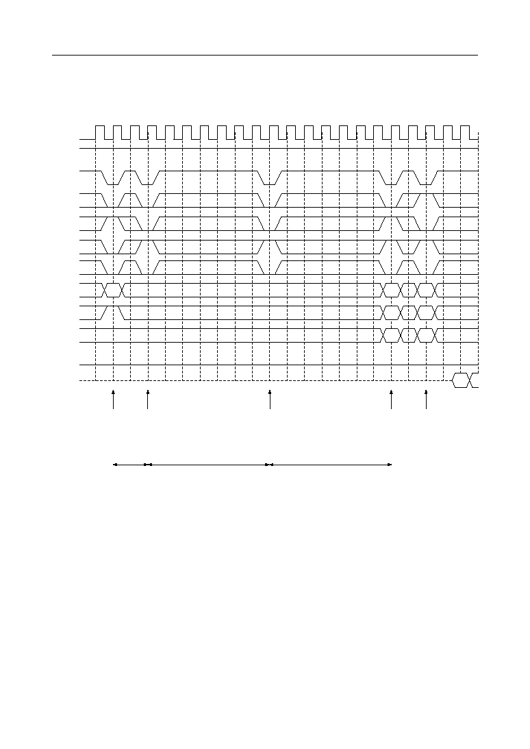
Power on Sequence and Auto Refresh (Initialization)
0
2
3
5
6
8
9
10 11
13
15
17 18
20 21
CLK
CKE
CS
RAS
CAS
WE
A9
(BA)
A8
ADD
DQM
0 - 3
DQ
DSF
PRE
(All Banks)
REF
REF
Hi-Z
t
RC
t
RC
MRA
~
~
Q
Q
z
z
P
P
~
P
Q
z
~
P
P
Q
Q
z
P
Q
z
~
~
P
Q
Q
,
y
|
~
Q
Q
,
y
Q
,
y
|
~
|
~
Q
z
z
~
P
P
Q
Q
P
z
P
P
z
P
z
P
~
P
Q
,
y
|
,
y
,
y
|
|
z
~
1
4
7
12
14
16
19
ADDRESS KEY
High level is necessary
8 refresh cycles are necessary
High level is necessary
38/66
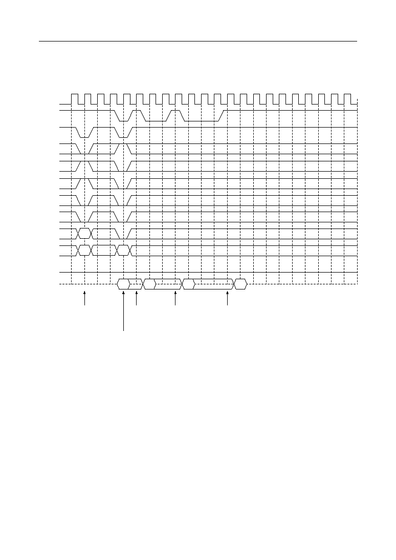
° Semiconductor
MSM54V25632A
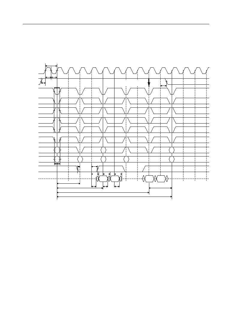
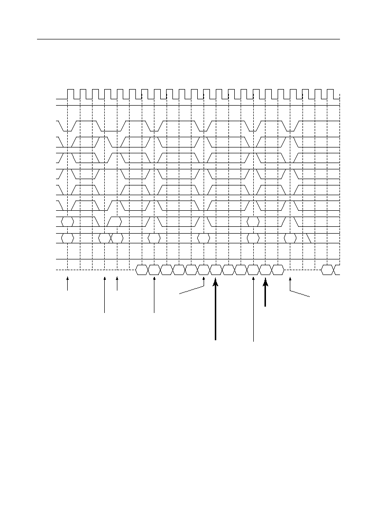
Mode Register Set
(BL = 4, CL = 2)
CLK
CKE
CS
RAS
CAS
WE
A9
(BA)
A8
ADD
DQM
0 - 3
DQ
0
2
3
4
5
6
9
11 12
14 15
17 18
20 21
DSF
PRE
(All Banks)
MRA
ACT
t
RP
Hi-Z
H
z
P
P
|
~
~
Q
Q
,
y
|
|
,
y
|
,
y
z
|
|
,
y
z
|
|
P
P
,
y
|
,
y
z
z
~
~
z
~
~
P
P
Q
Q
z
z
,
y
z
|
|
P
P
|
,
y
,
y
|
|
,
y
z
|
,
y
z
|
~
~
~
~
Q
Q
1
7
8
10
13
16
19
t
RSC
(20 ns)
ADDRESS KEY
39/66
° Semiconductor
MSM54V25632A
Auto Refresh
(CL = 2)
CLK
CKE
H
CS
RAS
CAS
WE
A9
(BA)
A8
ADD
DQM
0 - 3
DQ
0
DSF
PRE
REF
REF
ACT
RD
t
RP
t
RC
t
RC
z
z
P
z
P
z
P
P
|
,
y
|
~
~
Q
~
Q
Q
,
y
|
|
~
Q
Q
,
y
,
y
z
P
,
y
|
~
Q
,
y
|
~
Q
,
y
,
y
Q
~
z
z
~
~
P
Q
P
Q
z
P
Q
z
z
P
P
|
P
,
,
y
y
z
z
|
|
P
P
L
1
2
3
4
5
6
7
8
9
10 11 12 13 14 15 16 17 18 19 20 21
Q1

40/66
° Semiconductor
MSM54V25632A
Self Refresh (Entry and Exit)
CLK
CKE
CS
RAS
CAS
WE
A9
(BA)
A8
ADD
DQM
0 - 3
DQ
DSF
PRE
SREF
entry
SREF
Exit
SREF
entry
or
(ACT)
SREF
Exit
Next clock
enable
Next
clock
enable
ACT
t
RP
t
RC
t
RC
0
1
2
3
7
8
9
10 11
17 18 19 20 21
4
12
L
,
y
P
z
P
z
P
P
,
y
z
|
,
y
z
|
P
Q
,
y
|
~
z
,
y
|
~
Q
,
y
|
~
Q
|
~
Q
,
y
z
|
P
,
y
|
P
|
P
P
,
y
|
,
y
|
Q
~
Q
|
~
Q
Q
~
~
Q
z
z
P
P
z
z
z
z
P
P
41/66
° Semiconductor
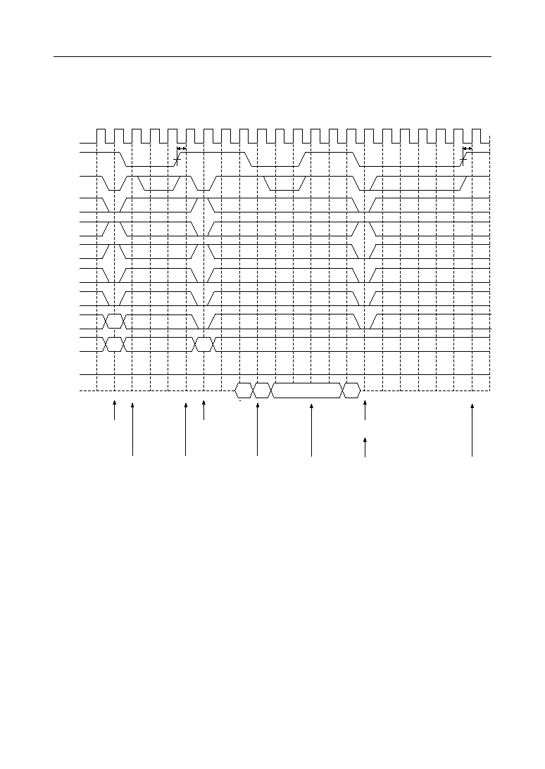
MSM54V25632A
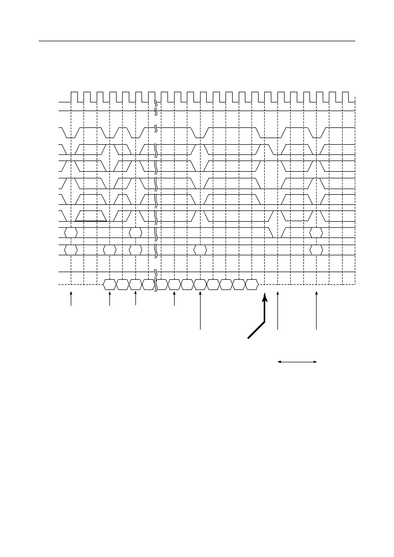
Auto Precharge after Read Burst
(BL = 4, CL = 3)
CLK
CKE
H
CS
RAS
CAS
WE
A9
(BA)
A8
ADD
DQM
0 - 3
DQ
0
DSF
ACT-A
ACT-B
RD-A
RAP-B
ACT-B
RAP-A
L
Hi-Z
AP-B
AP-A
RAP-B
,
y
|
~
z
~
z
z
|
~
Q
z
z
P
z
P
Q
z
P
Q
,
y
Q
,
,
y
y
|
|
|
P
z
P
|
~
~
~
Q
,
y
|
~
~
Q
,
y
|
~
Q
~
Q
~
P
Q
~
z
P
z
~
P
Q
~
z
~
z
P
P
,
y
|
|
,
y
|
|
,
y
,
y
|
1
2
3
4
5
6
7
8
9
10 11 12 13 14 15 16 17 18 19 20 21
QBb2
QBb1
QAb4
QAb3
QAb2
QAb1
QBa4
QBa3
QBa2
QBa1
QAa4
QAa3
QAa2
QAa1
CBb
RBb
CAa
CBa
RBa
CAb
RAa
RAa
RBb
RBa
42/66
° Semiconductor
MSM54V25632A
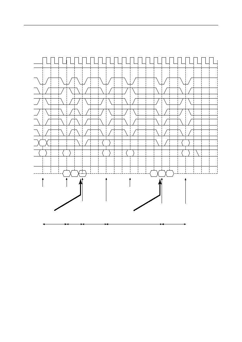
Auto Precharge after Write Burst
(BL = 4, CL = 3)
CLK
CKE
CS
RAS
CAS
WE
A9
(BA)
A8
ADD
DQM
0 - 3
DQ
DSF
H
0
ACT-A
ACT-B
WT-A
WAP-B
WAP-A
WAP-B
L
Hi-Z
AP-B
ACT-B
AP-A
|
|
|
~
Q
|
,
y
|
,
y
|
,
y
|
~
~
Q
Q
Q
,
y
Q
,
y
|
~
,
y
Q
P
z
P
P
z
z
z
P
,
y
P
Q
,
y
|
~
|
~
Q
,
y
|
,
y
|
,
y
~
Q
Q
~
Q
Q
~
~
Q
~
P
Q
z
P
Q
z
~
z
P
Q
P
Q
z
~
~
P
Q
1
2
3
4
5
6
7
8
9
10 11 12 13 14 15 16 17 18 19 20 21
DBb4
DBb3
DBb2
DBb1
DAb4
DAb3
DAb2
DAb1
DBa4
DBa3
DBa2
DBa1
DAa4
DAa3
DAa2
DAa1
CBb
RBb
CAa
CBa
RBa
CAb
RAa
RAa
RBb
RBa
43/66
° Semiconductor
MSM54V25632A
Full Page READ Cycle
(CL = 3)
CLK
CKE
H
CS
RAS
CAS
WE
A9
(BA)
A8
ADD
DQM
0 - 3
DQ
0
DSF
ACT-A
RD-A
ACT-B
RD-B
Burst cannot
end in Full
Page mode
PRE-B
ACT-B
L
Hi-Z
Burst stop
Command
t
RP
,
y
,
y
,
y
z
,
y
z
|
P
P
z
P
z
z
z
P
|
,
y
|
,
y
|
,
y
z
P
,
y
z
P
,
y
z
|
,
,
,
y
y
y
|
|
~
~
Q
Q
,
y
z
,
y
,
,
y
y
|
|
,
y
,
y
Q
,
y
Q
Q
|
~
|
Q
,
y
|
~
,
y
|
~
~
Q
~
Q
~
1
2
3
4
5
6
7
8
9
10 11 12 13 14 15 16 17 18 19 20 21
QBa+3 QBa+4 QBa+5
QBa+2
QBa+1
QBa
QAa+1
QAa
QAa≠1
QAa≠2
QAa+1
QAa
RBb
RBa
CBa
RBa
RBb
QAa≠3
CAa
RAa
RAa
44/66
° Semiconductor
MSM54V25632A
Full Page WRITE Cycle
(CL = 3)
CLK
CKE
H
CS
RAS
CAS
WE
A9
(BA)
A8
ADD
DQM
0 - 3
DQ
1
DSF
ACT-A
WT-A
ACT-B
Burst cannot
end in Full
Page mode
WT-B
PRE-B
ACT-B
L
Hi-Z
Burst stop
Command
t
RP
P
Q
~
P
Q
z
~
,
y
,
y
Q
Q
,
y
|
~
~
z
~
,
y
|
~
,
y
Q
Q
|
~
Q
z
z
P
Q
z
P
Q
~
Q
~
Q
z
z
P
P
P
Q
z
~
P
Q
z
z
~
P
P
Q
Q
P
P
z
z
z
,
y
|
z
P
z
P
,
y
,
y
,
y
|
,
y
|
0
3
2
5
4
7
6
9
8
11
10
13
12
15
14
17
16
19
18
21
20
RBb
RBb
CBa
CAa
RAa
RAa
RBa
RBa
DBa+3 DBa+4
DBa+2
DBa+1
DBa
DAa+1
DAa
DAa≠1
DAa+3
DAa+2
DAa+1
DAa
45/66
° Semiconductor
MSM54V25632A
PRE (Precharge) Termination of Burst
(BL = 2, 4, 8, Full, CL = 3)
CLK
CKE
CS
RAS
CAS
WE
A9
(BA)
A8
ADD
DQM
0 - 3
DQ
0
1
DSF
DQM
0 - 3
ACT-A
WT-A
RD-A
ACT-A
PRE-A
PRE Command
Termination
L
Hi-Z
H
PRE-A
ACT-A
PRE Command
Termination
t
DPL
t
RP
t
RP
t
RAS
t
RCD
~
~
~
Q
Q
,
y
z
P
,
y
z
P
P
|
P
,
y
z
P
,
y
z
|
,
y
z
|
|
|
,
y
,
y
|
,
y
|
|
~
Q
~
Q
Q
~
z
~
Q
~
z
~
z
P
Q
~
z
P
Q
P
Q
~
~
P
Q
z
~
z
P
P
z
P
~
~
Q
~
Q
Q
P
2
3
4
5
6
7
8
9
10 11 12 13 14 15 16 17 18 19 20 21
QAb3
QAb2
QAb1
DAa1
RAc
CAa
RAb
CAb
RAa
RAa
RAb
RAc
DAa2
46/66
° Semiconductor
MSM54V25632A
Clock Suspension during Burst Read (using CKE Function)
(BL = 4, CL = 3)
CLK
CKE
CS
RAS
CAS
WE
A9
(BA)
A8
ADD
DQM
0 - 3
DQ
0
DSF
DQM
0 - 3
ACT-A
RD-A
1-CLOCK
SUSPENDED
2-CLOCK
SUSPENDED
3-CLOCK
SUSPENDED
Hi-Z
(turn off)
at end of burst
L
z
z
P
P
|
,
,
y
y
z
z
|
|
P
P
|
,
,
y
y
|
|
~
~
~
Q
Q
z
z
P
P
|
P
P
|
,
,
y
y
z
z
|
|
P
P
P
|
P
~
Q
~
~
~
Q
Q
~
Q
|
1
2
3
4
5
6
7
8
9
10 11 12 13 14 15 16 17 18 19 20 21
QAa2
QAa3
QAa4
CAa
RAa
RAa
QAa1
47/66
° Semiconductor
MSM54V25632A
Clock Suspension during Burst Write (using CKE Function)
(BL = 4, CL = 3)
P
Q
z
z
~
~
P
P
Q
Q
P
z
z
P
P
,
,
y
y
|
|
z
z
~
~
P
P
Q
Q
z
z
P
Q
P
z
z
P
P
z
z
P
,
,
y
y
z
z
|
|
P
P
,
y
z
,
y
Q
~
~
Q
Q
,
y
|
|
|
CLK
CKE
CS
RAS
CAS
WE
A9
(BA)
A8
ADD
DQM
0 - 3
DQ
0
DSF
DQM
0 - 3
L
CAa
RAa
RAa
ACT-A
1-CLOCK
SUSPENDED
2-CLOCK
SUSPENDED
3-CLOCK
SUSPENDED
WT-A
DAa4
DAa3
DAa2
DAa1
1
2
3
4
5
6
7
8
9
10 11 12 13 14 15 16 17 18 19 20 21
48/66
° Semiconductor
MSM54V25632A
Power Down Mode and Clock Suspension
(BL = 4, CL = 2)
CLK
CKE
CS
RAS
CAS
WE
A9
(BA)
A8
ADD
DQM
0 - 3
DQ
0
DSF
DQM
0 - 3
L
VALID
ACT-A
RD-A
ACTIVE STANDBY
PRECHARGE STANDBY
PRE-A
PD
PD Entry
PD Exit
Clock Mask
Start
Clock Mask
End
PD
t
CKS
t
PDE
,
y
|
~
Q
z
~
,
y
|
~
,
y
~
~
Q
Q
,
y
|
~
|
,
y
|
|
~
~
Q
~
P
Q
P
z
~
~
P
Q
~
Q
~
~
~
Q
z
z
P
,
y
|
,
y
|
,
y
|
|
|
~
Q
,
y
|
|
~
~
Q
z
z
~
,
y
|
,
y
1
2
3
4
5
6
7
8
9
10 11 12 13 14 15 16 17 18 19 20 21
CAa
RAa
RAa
QAa4
QAa3
QAa2
QAa1
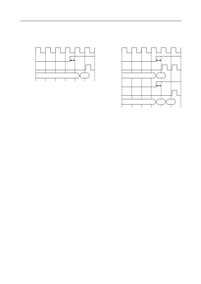
49/66
° Semiconductor
MSM54V25632A
CLOCK Suspend Exit & Power Down Exit
,
CLK
2) Power Down (= Precharge Power Down) Exit
(CASE 1)
CKE
Internal
CLK
Command
(CASE 2)
CKE
Internal
CLK
Command
Note 2
ACT
NOP
ACT
t
PDE
Note 2
< t
PDE
Note 3
Note 4
CLK
1) Clock Suspend (= Active Power Down) Exit
CKE
Internal
CLK
Command
Note 1
RD
t
CKS
Notes: 1.
Active power down: one or both bank active state.
2.
Precharge power down: both bank precharge state.
3.
t
PDE
: Asynchronous AC parameter. Time for Power Down Exit Setup Time. Only
valid at precharge power down exit.
4.
t
CKS
< t
PDE
, NOP should be issued. And new command can be issued after 1 Clock.
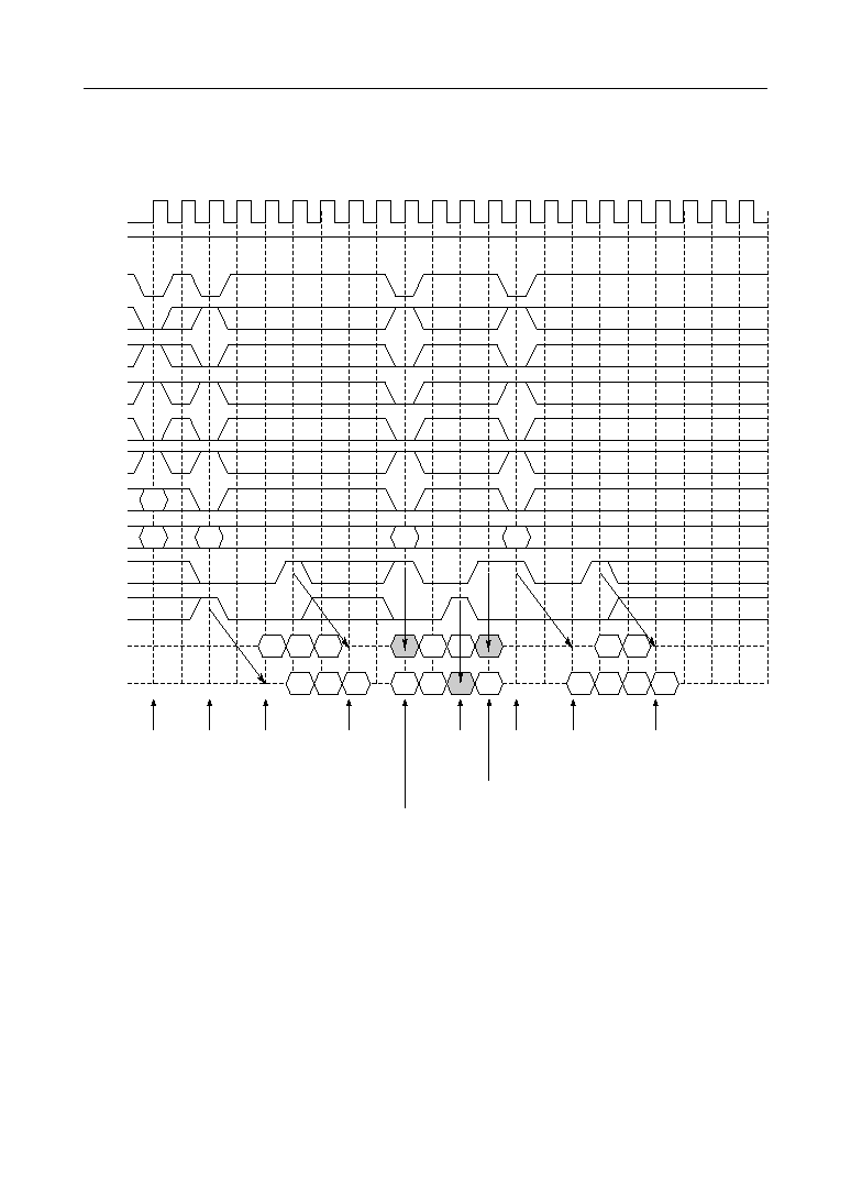
50/66
° Semiconductor
MSM54V25632A
Byte Read/Write Operation (by DQM)
(BL = 4, CL = 2)
CLK
CKE
CS
RAS
CAS
WE
A9
(BA)
A8
ADD
DQM
DQM1
0
DSF
DQM0
H
ACT-B
RD-B
Byte of
DQ8 - 15
not Read
Byte of
DQ0 - 7
not Read
Byte of DQ0 - 7
not Write
WT-B
Byte of
DQ8 - 15
not Write
Byte of
DQ0 - 7
not Read
Byte of
DQ0 - 7
not Read
Byte of DQ0 - 7
not Write
DQ
0 - 7
DQ
8 - 15
Q
P
,
y
z
P
Q
z
P
,
y
|
~
Q
~
P
Q
z
~
P
Q
z
z
z
P
z
P
,
y
|
~
Q
,
y
Q
~
P
Q
Q
~
Q
~
Q
Q
P
Q
z
~
P
Q
,
y
|
,
y
,
y
|
,
y
,
y
Q
z
P
Q
P
P
z
P
,
y
|
~
Q
,
y
|
~
Q
,
y
Q
~
~
Q
Q
1
2
3
4
5
6
7
8
9
10 11 12 13 14 15 16 17 18 19 20 21
QBa4
QBa3
QBa2
DBb2
DBb1
DBb4
QBc2
QBc1
QBc3 QBc4
QBa1
QBa3
QBa2
DBb2 DBb3
QBc2 QBc3
RBa
RBa
CBa
CBb
CBc
RD-B
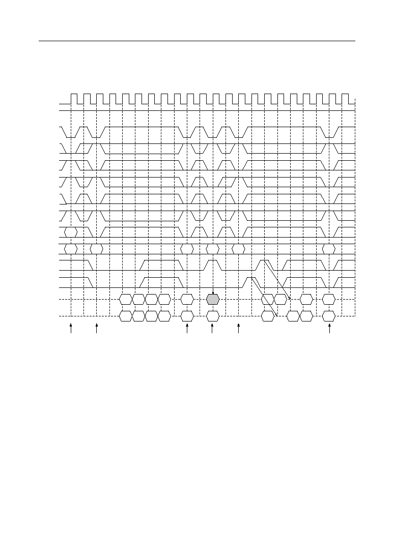
51/66
° Semiconductor
MSM54V25632A
Burst Read and Single Write
(BL = 4, CL = 2)
CLK
CKE
CS
RAS
CAS
WE
A9
(BA)
A8
ADD
DQM1
DQ
0 - 7
DQ
8 - 15
0
DSF
DQM0
ACT-B
RD-B
Single
WT
Single
WT
RD
Single
WT
H
Write
Masking
z
z
P
P
P
,
y
P
P
z
P
,
y
Q
Q
z
,
y
|
~
z
P
,
y
|
P
|
z
~
Q
Q
z
P
,
y
P
P
Q
,
y
z
|
,
y
z
|
P
z
P
,
y
z
P
Q
P
|
P
|
~
Q
P
,
y
|
|
,
y
z
P
Q
,
y
Q
Q
Q
Q
,
y
Q
~
,
y
|
~
~
Q
,
y
|
~
Q
~
Q
|
~
Q
1
2
3
4
5
6
7
8
9
10 11 12 13 14 15 16 17 18 19 20 21
QBa1 QBa2 QBa3 QBa4
DBb
DBc
CBb
CBc
CBd
CBe
DBe
QBd1
CBa
RBa
RBa
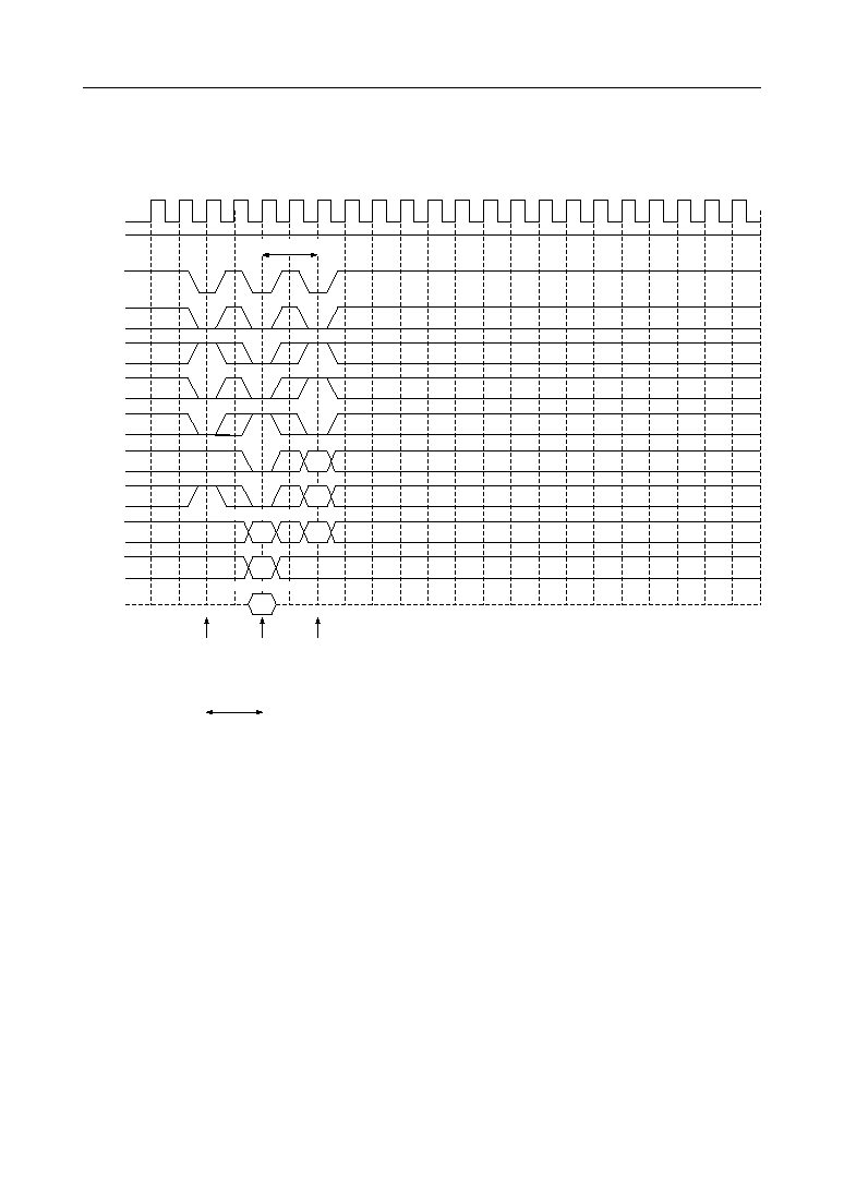
52/66
° Semiconductor
MSM54V25632A
Special Mode Register Set
(BL = 4, CL = 2)
z
P
,
y
Q
z
P
|
~
Q
~
Q
z
~
P
Q
|
P
,
y
z
P
,
y
,
y
Q
z
z
P
~
~
Q
,
,
y
y
|
|
,
,
y
y
|
|
~
~
Q
z
z
z
~
~
P
Q
z
z
z
P
,
y
z
,
,
y
y
z
z
|
|
P
,
y
z
|
P
,
,
y
y
|
|
,
y
|
CLK
CKE
CS
RAS
CAS
WE
A9
(BA)
A8
ADD
DQM
0 - 3
DQ
0
DSF
SMRA
PRE
(All Banks)
Remark Special Register Set command can be input at any state.
ACT
is valid
H
Hi-Z
t
RP
1
2
3
4
5
6
7
8
9
10 11 12 13 14 15 16 17 18 19 20 21
t
RSC
(20 ns)
ADDRESS KEY
Color or Mask data
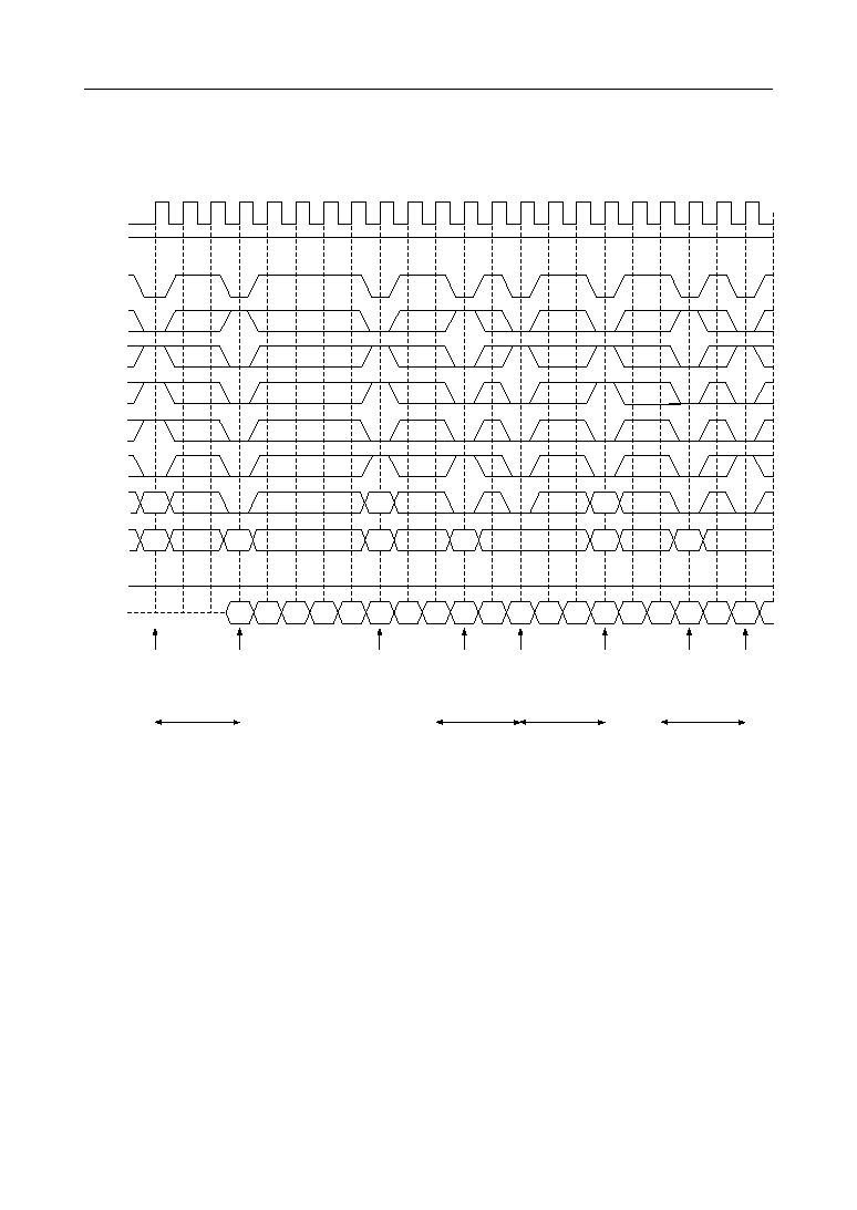
53/66
° Semiconductor
MSM54V25632A
Random Row Write with WPB
(BL = 8, CL = 3)
,
y
|
~
~
z
~
Q
~
~
Q
~
P
Q
,
y
Q
Q
z
P
z
z
,
y
,
y
z
P
P
z
z
~
z
|
|
~
,
y
,
y
Q
P
|
|
~
Q
~
P
Q
|
~
Q
,
y
|
,
y
z
P
Q
z
,
y
z
z
|
,
y
z
P
z
P
z
,
y
~
,
y
|
|
,
y
,
y
|
CLK
CKE
CS
RAS
CAS
WE
A9
(BA)
A8
ADD
DQ
0
DSF
DQM
0 - 3
ACT-A
with WPB
WT-A
WPB is enabled.
ACT-B
WT-B
WPB is disabled.
WT-A
WPB is disabled.
PRE-A
PRE-B
ACT-A
H
L
t
RCD
t
DPL
t
RP
t
DPL
DAa1 DAa2 DAa3 DAa4 DAa5 DAa6 DAa7 DAa8 DBa1 DBa2 DBa3 DBa4 DBa5 DBa6 DBa7 DBa8 DAb1 DAb2 DAb3
RAa
RAa
CAa
RBa
RBa
CBa
RAb
RAb
CAb
1
2
3
4
5
6
7
8
9
10 11 12 13 14 15 16 17 18 19 20 21
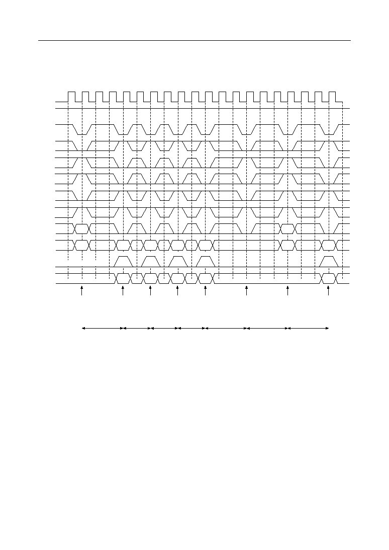
54/66
° Semiconductor
MSM54V25632A
Block Write (Page at Same Bank)
(CL = 3)
CLK
CKE
CS
RAS
CAS
WE
A9
(BA)
A8
ADD
DQ
0
DSF
DQM
0 - 3
ACT-B
BW-B
BW-B
BW-B
BW-B
BW-B
WPB is enabled.
PRE-B
ACT-B
with WPB
H
t
RCD
t
RCD
t
RP
t
BPL
t
BWC
t
BWC
z
z
z
P
Q
~
P
Q
|
~
Q
P
z
P
Q
,
y
Q
,
y
,
y
Q
P
z
~
~
P
Q
|
~
Q
z
P
z
,
y
|
~
|
z
z
~
~
,
y
Q
~
Q
Q
,
y
|
~
~
,
y
|
~
|
~
~
~
z
P
~
|
~
~
z
P
Q
z
P
Q
z
~
~
P
Q
P
,
y
|
z
P
z
z
z
z
P
,
y
,
y
|
|
,
y
|
|
|
,
y
,
y
|
|
|
z
z
~
~
~
P
Q
|
~
Q
,
y
1
2
3
4
5
6
7
8
9
10
11
12
13
14
15
16
17
18
19
RBa
RBa
CBa
CM
CBb
CBc
CBd
CM
CM
CM
CM
I/O Mask
I/O Mask
I/O Mask
I/O Mask
L = No I/O Mask
RBb
CBc
RBb
I/O Mask
t
BWC
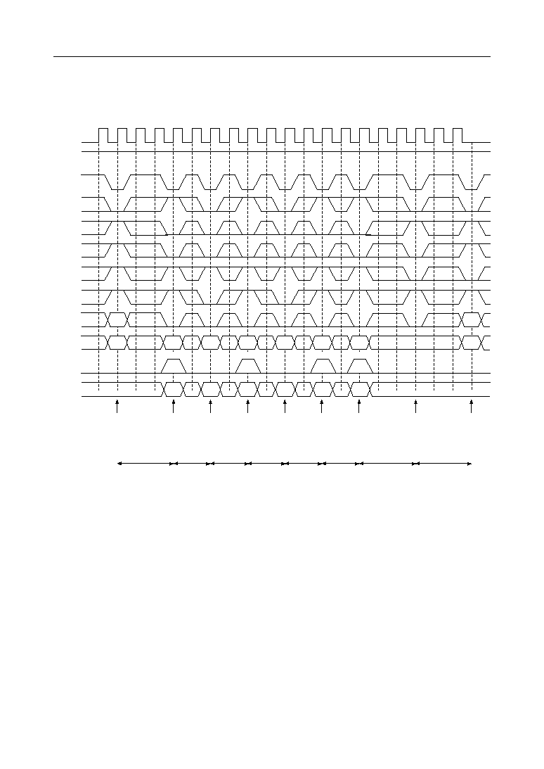
55/66
° Semiconductor
MSM54V25632A
Block Write (Page at Same Bank) Changing Color and Mask Data
(CL = 3)
Q
Q
~
~
,
y
Q
z
P
,
y
|
~
~
|
~
Q
,
y
Q
,
y
|
~
z
P
Q
~
Q
Q
~
Q
P
Q
z
P
Q
z
z
~
~
~
P
Q
,
y
,
y
,
y
|
|
|
z
~
z
~
P
Q
,
y
|
~
Q
P
,
y
z
P
,
y
|
|
P
z
P
z
z
|
~
,
y
,
y
|
,
y
|
|
Q
,
y
z
,
y
,
y
|
,
y
z
,
y
|
~
~
Q
Q
~
~
~
Q
P
z
P
z
z
z
P
CLK
CKE
CS
RAS
CAS
WE
A9
(BA)
A8
ADD
DQ
0
DSF
DQM
0 - 3
ACT-B
with WPB
BW-B
SMRA
(Mask data)
BW-B
SMRA
(Color data)
PRE-B
ACT-B
BW-B
BW-B
H
t
RCD
t
BPL
t
BWC
t
RSC
(20 ns)
t
BWC
t
RSC
(20 ns)
t
BWC
t
RCD
CM
RBa
RBa
CBa
20h
CBb
40h
CBc
CBd
RBb
RBb
Mask
CM
Color
CM
CM
I/O Mask
I/O Mask
I/O Mask
I/O Mask
1
2
3
4
5
6
7
8
9
10
11
12
13
14
15
16
17
18
19
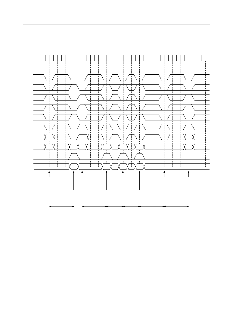
56/66
° Semiconductor
MSM54V25632A
Interleaved Block Write
(CL = 3)
CLK
CKE
CS
RAS
CAS
WE
A9
(BA)
A8
ADD
DQ
0
DSF
DQM
0 - 3
ACT-A
BW-A
BW-B
BW-B
BW-A
ACT-B
PRE-B
H
L
t
RP
t
BPL
t
BWC
t
BWC
t
RCD
t
RCD
Column Mask
z
|
z
~
Q
~
z
~
~
Q
,
y
|
P
~
~
~
P
Q
,
y
z
z
~
~
z
P
Q
~
P
Q
z
P
Q
z
P
,
y
Q
~
Q
Q
Q
,
y
z
|
~
Q
~
~
Q
P
,
y
z
,
y
z
|
,
y
z
|
P
P
,
y
z
|
,
y
|
|
P
|
,
y
z
P
,
y
z
|
,
y
z
|
1
2
3
4
5
6
7
8
9
10
11
12
13
14
15
16
17
18
19
ACT-B
CM
RAa
RAa
CAa RBa
CBa
CAb
CBb
RBa
CM
CM
CM
RBb
RBb
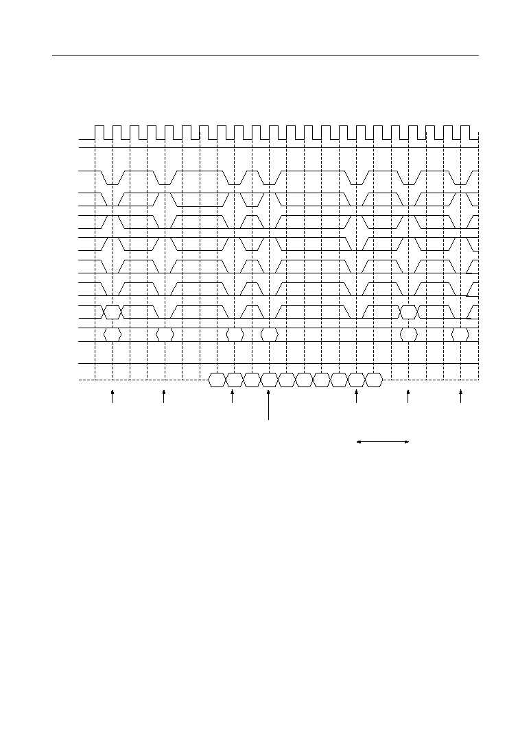
57/66
° Semiconductor
MSM54V25632A
Random Column Read (Page with Same Bank)
(BL = 4, CL = 3)
~
~
Q
Q
Q
~
z
P
Q
z
P
z
P
,
y
|
~
,
y
Q
z
P
Q
z
P
Q
z
~
Q
,
y
|
~
Q
~
Q
,
y
Q
z
P
Q
Q
P
~
z
|
~
~
Q
P
Q
~
P
Q
Q
P
Q
,
y
|
~
,
y
|
~
Q
,
y
Q
|
,
y
,
y
|
~
,
y
Q
Q
,
y
|
|
,
y
Q
CLK
CKE
CS
RAS
CAS
WE
A9
(BA)
A8
ADD
DQ
0
DSF
DQM
0 - 3
ACT-A
RD-A
RD-A
PRE-A
ACT-A
RD-A
RD-A
H
L
t
RP
RAa
RAa
CAa
CAb
CAc
RAa
CAa
RAa
QAa1 QAa2 QAa3 QAa4 QAb1 QAb2 QAc1 QAc2 QAc3 QAc4
1
2
3
4
5
6
7
8
9
10 11 12 13 14 15 16 17 18 19 20 21

58/66
° Semiconductor
MSM54V25632A
Random Column Write (Page with Same Bank)
(BL = 4, CL = 3)
CLK
CKE
CS
RAS
CAS
WE
A9
(BA)
A8
ADD
DQ
0
DSF
DQM
0 - 3
ACT-B
WT-B
WT-B
WT-B
WT-B
ACT-B
PRE-B
H
L
t
RP
DBb2 DBc1 DBc2 DBc3 DBc4
DBd1
DBa2
DBa1
DBa3 DBa4 DBb1
1
2
3
4
5
6
7
8
9
10 11 12 13 14 15 16 17 18 19 20 21
P
z
P
z
P
z
z
P
z
z
,
y
|
Q
~
~
Q
Q
Q
~
,
y
z
P
,
y
z
,
y
z
|
,
y
z
|
|
P
,
y
z
P
,
y
z
P
,
,
,
y
y
y
z
z
z
|
|
P
P
RBa
CBa
CBb
CBc
RBd
CBd
P
P
z
P
z
z
P
z
z
z
RBa
RBd
z
P
Q
z
~
~
P
Q
z
P
Q
z
P
Q
z
~
z
,
y
,
y
|
,
y
,
y
,
y
|
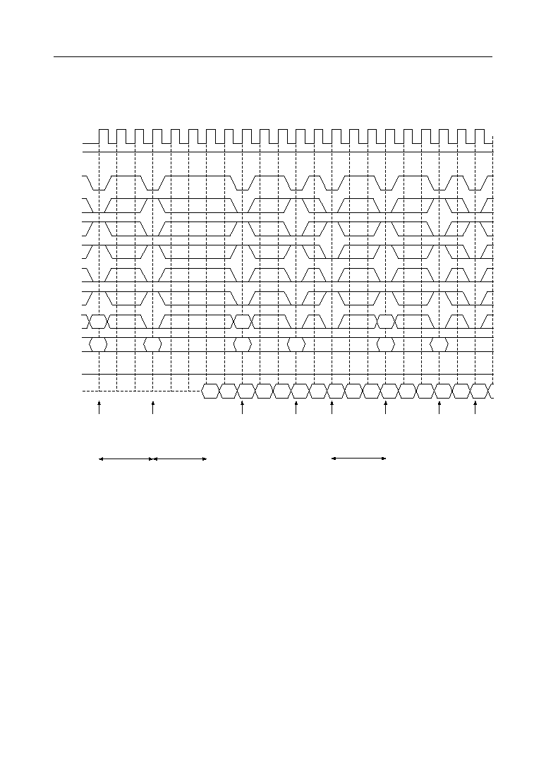
59/66
° Semiconductor
MSM54V25632A
Random Row Read
(BL = 8, CL = 3)
,
,
y
y
z
z
|
|
|
P
P
~
Q
~
z
~
Q
Q
~
Q
P
z
~
Q
P
~
|
~
|
~
P
Q
,
y
z
P
|
P
,
y
z
|
P
z
z
P
z
~
|
,
y
|
|
P
,
y
z
|
,
y
z
P
z
P
z
P
Q
P
z
|
~
~
|
~
P
Q
P
Q
z
P
Q
,
y
|
,
y
,
y
P
|
z
P
P
P
z
z
CLK
CKE
CS
RAS
CAS
WE
A9
(BA)
A8
ADD
DQ
0
DSF
DQM
0 - 3
ACT-B
ACT-B
ACT-A
RD-B
RD-B
RD-A
PRE-B
PRE-A
H
L
t
RP
t
RCD
CL
RBa
RBa
RAa
RBb
CBa
RAa
CAa
RBb
CBb
QAa1 QAa2 QAa3 QAa4 QAa5 QAa6 QAa7
QBa2
QBa1
QBa3 QBa4 QBa5 QBa6 QBa7 QBa8
QAa8
1
2
3
4
5
6
7
8
9
10 11 12 13 14 15 16 17 18 19 20 21
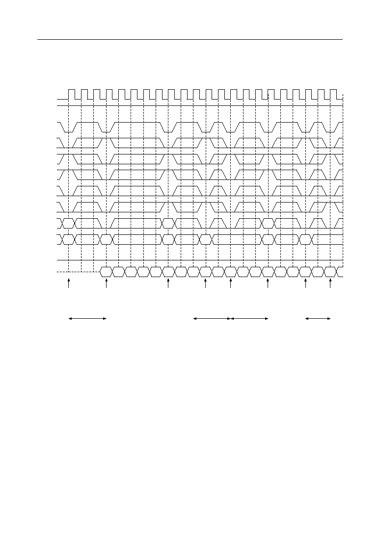
60/66
° Semiconductor
MSM54V25632A
Random Row Write
(BL = 8, CL = 3)
|
P
|
P
,
y
z
,
y
,
y
z
P
P
|
P
~
Q
z
Q
~
|
|
|
~
z
P
Q
~
P
Q
z
~
~
Q
~
~
P
Q
~
z
P
,
y
P
P
z
z
Q
~
Q
|
~
~
,
y
z
|
~
|
~
,
y
|
P
Q
~
,
y
|
|
Q
Q
~
Q
~
~
~
Q
~
Q
Q
~
~
~
CLK
CKE
CS
RAS
CAS
WE
A9
(BA)
A8
ADD
DQ
0
DSF
DQM
0 - 3
ACT-A
ACT-A
PRE-A
PRE-B
WT-A
WT-B
WT-A
H
L
t
DPL
t
RCD
t
RP
t
DPL
DBa1 DBa2 DBa3 DBa4 DBa5 DBa6 DBa7 DBa8 DAb1 DAb2 DAb3
DAa2
DAa1
RAa
CBa
RAb
RAb
CAb
DAa3 DAa4 DAa5
DAa7 DAa8
RAa
CAa
1
2
3
4
5
6
7
8
9
10 11 12 13 14 15 16 17 18 19 20 21
ACT-B
RBa
RBa
DAa6
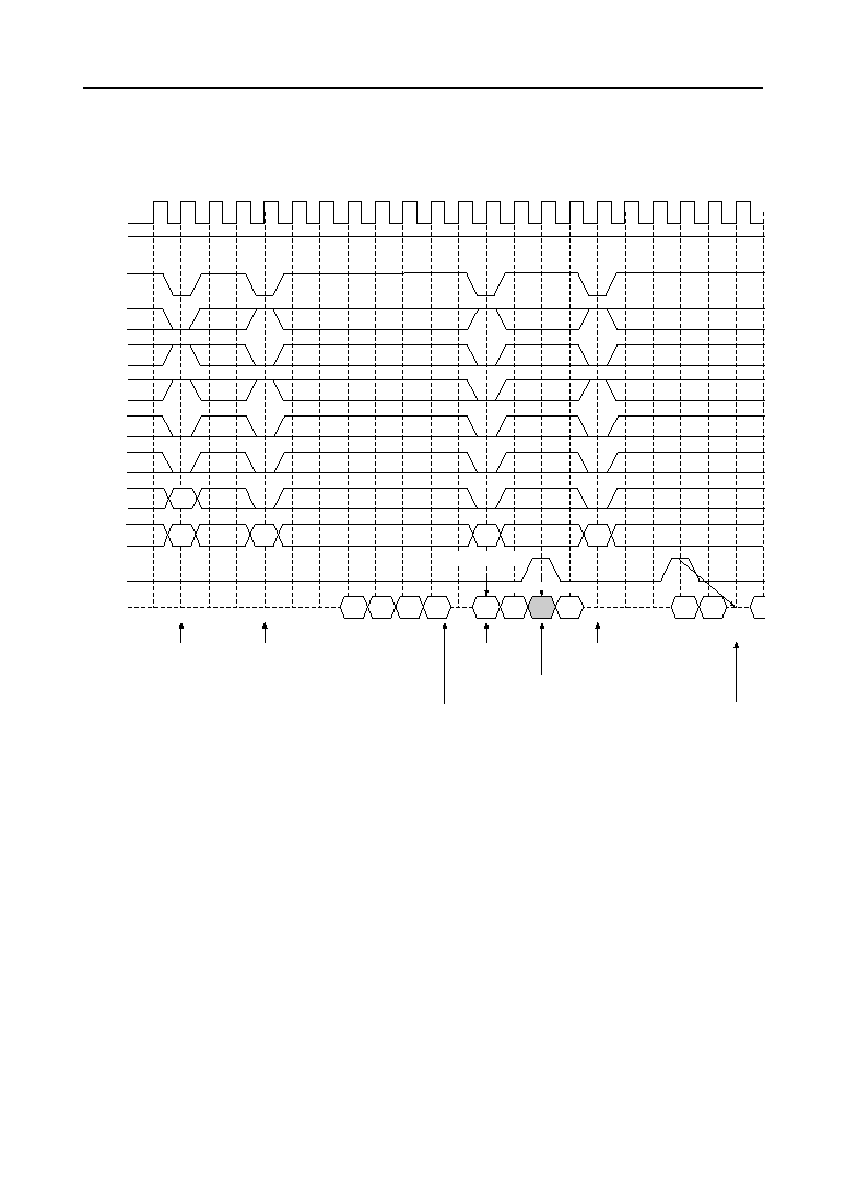
61/66
° Semiconductor
MSM54V25632A
READ and WRITE
(BL = 4, CL = 3)
~
z
~
,
y
|
~
Q
,
y
|
~
z
,
y
,
y
z
,
y
|
,
y
|
,
y
|
|
~
Q
,
y
|
z
P
z
P
|
,
y
z
|
,
y
z
|
,
y
z
|
P
z
,
y
z
z
|
P
z
~
P
Q
z
P
z
~
z
~
P
Q
z
P
CLK
CKE
CS
RAS
CAS
WE
A9
(BA)
A8
ADD
DQ
0
DSF
DQM
0 - 3
ACT-A
RD-A
WT-A
RD-A
Hi-Z at the end of Burst function
0-clock latency
2-clock latency
Hi-Z
H
RAa
CAa
CAb
CAc
DAb1 DAb2
DAb4
QAc1 QAc2
QAa1
RAa
QAa2 QAa3 QAa4
1
2
3
4
5
6
7
8
9
10 11 12 13 14 15 16 17 18 19 20 21
Write latency = 0
Write Masking
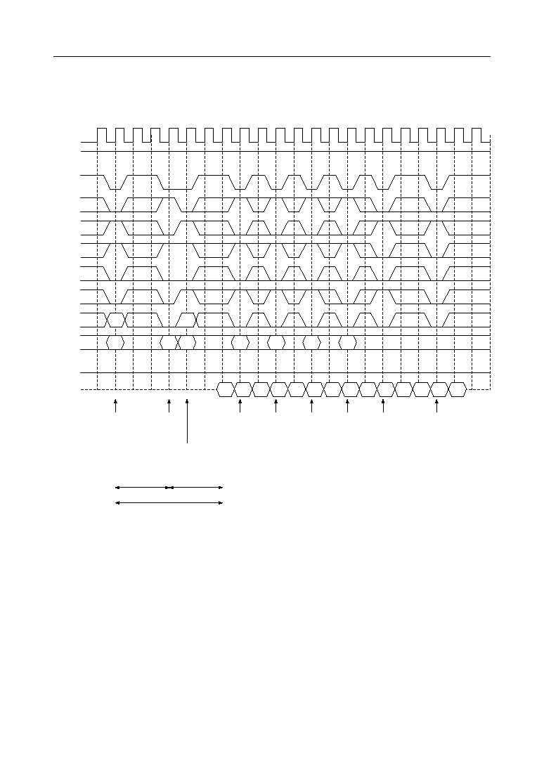
62/66
° Semiconductor
MSM54V25632A
Interleaved Column READ Cycle
(BL = 4, CL = 3)
~
~
Q
Q
Q
Q
P
P
z
,
y
|
z
P
z
|
~
Q
,
y
z
,
y
z
|
~
Q
~
,
y
|
~
|
|
~
~
Q
~
,
y
|
Q
Q
,
y
Q
,
y
P
P
P
P
Q
,
y
Q
,
y
|
~
|
~
Q
Q
P
P
z
z
P
|
,
y
z
~
Q
Q
,
y
|
~
,
y
|
~
Q
CLK
CKE
CS
RAS
CAS
WE
A9
(BA)
A8
ADD
DQ
0
DSF
DQM
0 - 3
ACT-A
RD-A
RD-B
RD-B
RD-B
RD-A
PRE-B
PRE-A
ACT-B
H
L
t
RCD
t
RRD
CL
RAa
CAa RBa
CBa
CBb
CBc
CAb
RAa
QBc1 QBc2 QAb1 QAb2 QAb3 QAb4
QAa2
QAa1
QAa3 QAa4 QBa1 QBa2 QBb1 QBb2
RBa
1
2
3
4
5
6
7
8
9
10 11 12 13 14 15 16 17 18 19 20 21
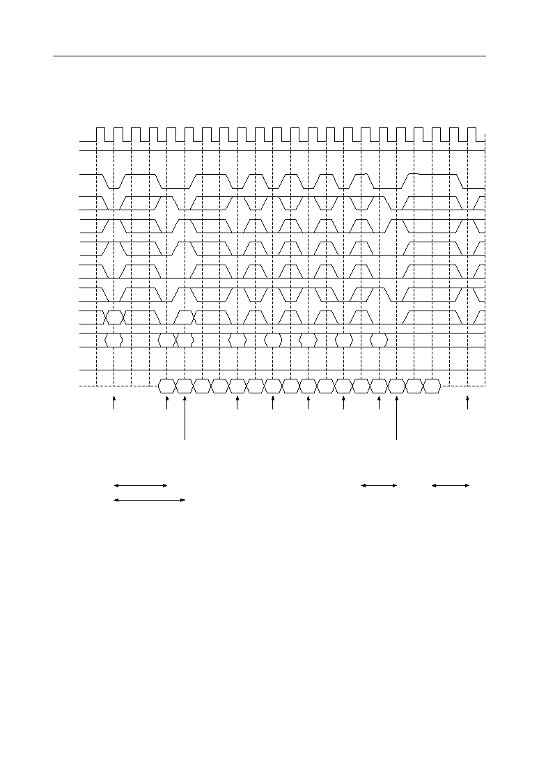
63/66
° Semiconductor
MSM54V25632A
Interleaved Column WRITE Cycle
(BL = 4, CL = 3)
z
z
P
P
P
P
|
|
,
y
|
~
Q
Q
|
~
Q
Q
z
~
~
P
Q
|
~
Q
~
Q
P
|
z
~
P
Q
Q
z
,
y
P
Q
~
~
~
P
Q
P
Q
,
y
|
,
y
|
~
|
|
~
~
~
P
Q
P
Q
z
~
~
~
~
z
~
P
Q
~
P
Q
z
CLK
CKE
CS
RAS
CAS
WE
A9
(BA)
A8
ADD
DQ
0
DSF
DQM
0 - 3
ACT-A
WT-A
WT-B
WT-B
WT-B
WT-A
WT-B
PRE-B
ACT-B
PRE-A
H
L
t
RCD
t
RRD
t
DPL
t
DPL
RAa
CAa RBa
CBa
CBb
CBc
CAb
CBd
RAa
DBc1 DBc2 DAb1 DAb2 DBd1 DBd2 DBd3 DBd4
DAa2
DAa1
DAa3 DAa4 DBa1 DBa2 DBb1 DBb2
RBa
1
2
3
4
5
6
7
8
9
10 11 12 13 14 15 16 17 18 19 20 21
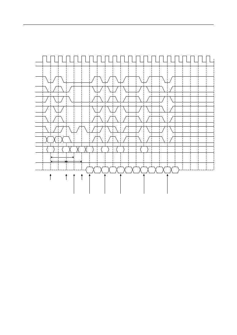
64/66
° Semiconductor
MSM54V25632A
Full Page Random Column Read
(BL = Full Page, CL = 2)
,
,
y
y
|
|
|
,
y
P
Q
,
y
|
|
~
~
Q
|
~
|
~
P
z
P
z
,
y
z
|
P
,
y
z
,
y
z
|
|
Q
~
~
~
Q
~
Q
,
y
z
,
y
z
|
|
P
,
y
z
|
P
Q
P
,
y
|
z
P
P
|
CLK
CKE
CS
RAS
CAS
WE
A9
(BA)
A8
ADD
DQ
0
DSF
DQM
0 - 3
ACT-A
ACT-B
RD-B
RD-A
RD-A
RD-A
RD-B
RD-B
PRE-B
(PRE Termination)
H
L
t
RCD
t
RRD
t
RCD
RAa
RBa CAa CBa CAb
CBb
CAc
CBc
QAc3 QBc1 QBc2 QBc3
Hi-Z
QBa1
QAa1
QAb1 QAb2 QBb1 QBb2 QAc1 QAc2
RBa
RAa
1
2
3
4
5
6
7
8
9
10 11 12 13 14 15 16 17 18 19 20 21
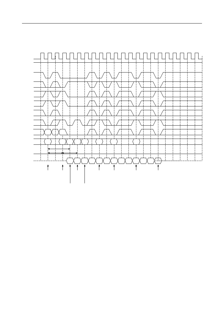
65/66
° Semiconductor
MSM54V25632A
Full Page Random Column Write
(BL = Full Page, CL = 2)
z
z
P
P
,
y
z
P
|
~
,
y
z
,
y
z
|
,
y
Q
,
y
,
y
|
~
|
~
Q
|
~
~
|
|
|
P
~
Q
~
P
z
P
z
P
z
z
|
,
y
,
y
Q
z
P
z
z
P
z
P
|
|
~
Q
,
y
z
P
Q
,
y
,
y
,
y
|
P
CLK
CKE
CS
RAS
CAS
WE
A9
(BA)
A8
ADD
DQ
0
DSF
DQM
0 - 3
ACT-A
ACT-B
WT-B
WT-B
WT-B
PRE-B
(PRE Termination)
WT-A
WT-A
WT-A
H
L
t
RCD
t
RRD
t
RCD
RAa
RBa CAa CBa CAb
CBb
CAc
CBc
DAc3 DBc1 DBc2 DBc3
DBa1
DAa1
DAb1 DAb2 DBb1 DBb2 DAc1 DAc2
RBa
RAa
1
2
3
4
5
6
7
8
9
10 11 12 13 14 15 16 17 18 19 20 21
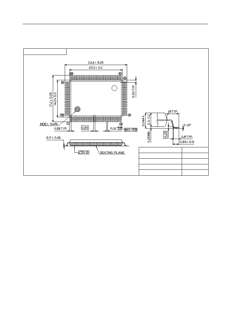
66/66
° Semiconductor
MSM54V25632A
(Unit : mm)
PACKAGE DIMENSIONS
Notes for Mounting the Surface Mount Type Package
The SOP, QFP, TSOP, TQFP, LQFP, SOJ, QFJ (PLCC), SHP, and BGA are surface mount type
packages, which are very susceptible to heat in reflow mounting and humidity absorbed in
storage. Therefore, before you perform reflow mounting, contact Oki's responsible sales person
on the product name, package name, pin number, package code and desired mounting conditions
(reflow method, temperature and times).
QFP100-P-1420-0.65-BK4
Package material
Lead frame material
Pin treatment
Solder plate thickness
Package weight (g)
Epoxy resin
42 alloy
Solder plating
5 mm or more
1.54 TYP.
Mirror finish

NOTICE
1.
The information contained herein can change without notice owing to product and/or
technical improvements. Before using the product, please make sure that the information
being referred to is up-to-date.
2.
The outline of action and examples for application circuits described herein have been
chosen as an explanation for the standard action and performance of the product. When
planning to use the product, please ensure that the external conditions are reflected in the
actual circuit, assembly, and program designs.
3.
When designing your product, please use our product below the specified maximum
ratings and within the specified operating ranges including, but not limited to, operating
voltage, power dissipation, and operating temperature.
4.
Oki assumes no responsibility or liability whatsoever for any failure or unusual or
unexpected operation resulting from misuse, neglect, improper installation, repair, alteration
or accident, improper handling, or unusual physical or electrical stress including, but not
limited to, exposure to parameters beyond the specified maximum ratings or operation
outside the specified operating range.
5.
Neither indemnity against nor license of a third party's industrial and intellectual property
right, etc. is granted by us in connection with the use of the product and/or the information
and drawings contained herein. No responsibility is assumed by us for any infringement
of a third party's right which may result from the use thereof.
6.
The products listed in this document are intended for use in general electronics equipment
for commercial applications (e.g., office automation, communication equipment,
measurement equipment, consumer electronics, etc.). These products are not authorized
for use in any system or application that requires special or enhanced quality and reliability
characteristics nor in any system or application where the failure of such system or
application may result in the loss or damage of property, or death or injury to humans.
Such applications include, but are not limited to, traffic and automotive equipment, safety
devices, aerospace equipment, nuclear power control, medical equipment, and life-support
systems.
7.
Certain products in this document may need government approval before they can be
exported to particular countries. The purchaser assumes the responsibility of determining
the legality of export of these products and will take appropriate and necessary steps at their
own expense for these.
8.
No part of the contents cotained herein may be reprinted or reproduced without our prior
permission.
9.
MS-DOS is a registered trademark of Microsoft Corporation.
Copyright 1999 Oki Electric Industry Co., Ltd.
Printed in Japan
E2Y0002-29-11