
° Semiconductor
MSM6262-xx
1/52
GENERAL DESCRIPTION
The MSM6262-xx is a dot matrix LCD controller which is fabricated by OKI's low power
consumption CMOS silicon gate technology. In combination with 8-bit microcontroller, the
MSM6262-xx can control the dot matrix character type LCD module.
The MSM6262-xx is provided with a serial data transfer output. So, a maximum of 160 characters
can be controlled by combining this device with the MSM5259, MSM5839C, or MSM5260.
The MSM6262-xx is recommended for use in an LCD panel which is capable of displaying 81 to
160 characters. If an LCD panel of which display capacity is 80 characters or less is used, the
MSM6222B-xx is recommended.
The MSM6262-xx is best suited to be used as an LCD controller for applications such as electronic
typewriters, POS system terminals, and data banks.
FEATURES
∑ Dot matrix LCD controller/driver for three different font configuration
(5 x 7 dots, 5 x 11 dots and 5 x 12 dots)
∑ Up to 160 characters can be controlled
(Display data RAM ... 160 x 9-bit)
∑ On-chip character generator ROM (CGROM) for 256 different characters
5 x 7 dots ... 128 characters
5 x 11 dots ... 96 characters
5 x 12 dots ... 32 characters
∑ On-chip character generator RAM (CGRAM) (32 x 8-bit)
5 x 8 dots ... 4 kinds
5 x 12 dots ... 2 kinds
∑ Easy interface with Z80, 6809, 80C49, and 80C51
∑ Underline function
∑ Shift function for g, i, p, q and y
∑ Selectable driving duty
° Semiconductor
MSM6262-xx
DOT MATRIX LCD CONTROLLER WITH 48-DOT COMMON DRIVER
E2B0033-27-Y2
Duty
Font Configuration (dots)
Cursor Display
Display (characters x lines)
1/16
5 x 7
80 x 2
1/24
5 x 11
80 x 2
1/32
5 x 7
40 x 4
1/48
5 x 11
40 x 4
Available
Available
Available
Available
∑ Package :
80-pin plastic QFP (QFP80-P-1420-0.80-BK) (Product name : MSM6262-xxGS-BK)
xx indicates code number.
This version: Nov. 1997
Previous version: Mar. 1996
° Semiconductor
MSM6262-xx
2/52
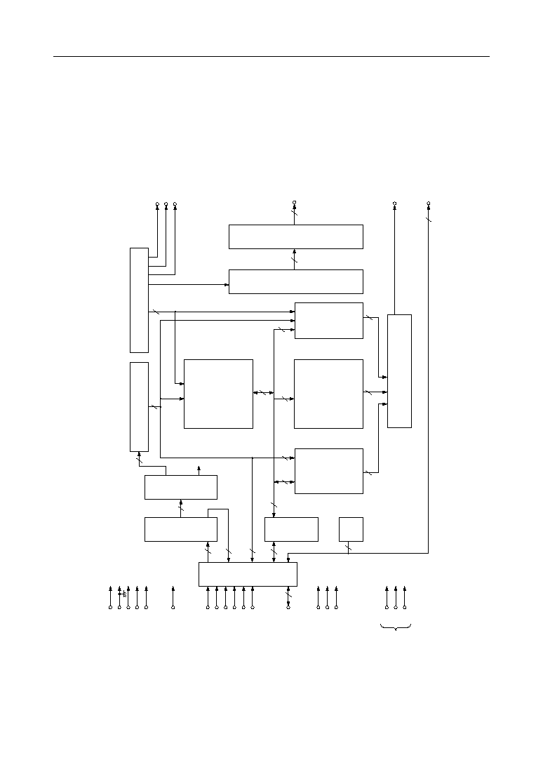
BLOCK DIAGRAM
V
DD
V
SS
OSC1
OSC2
OSC3
RESET
68 series/80 series
CS
R/W
(
WR
)
E
(
RD
)
A0
A1
8
DB
0
- DB
7
TEST1
TEST2
TEST3
V
1
V
4
V
5
LCD driving
voltage
Input/
Output
buffer
9
6
8
8
2
Instruc-
tion
register
(I/R)
Instruc-
tion
decoder
9
8
Address counter (ADC)
8
Display data RAM
(DDRAM)
160 x 9 bits
8
Timing generator
48
48
CP
LOAD
DF
DO
BUSY1 OUT
BUSY2 OUT
48-bit
shift
register
COM-
MON
signal
driver
1
1
Cursor
blink,
under-line
function
control
Character generator
ROM (CGROM),
11,680 bits
8
9
5
Parallel / Serial converter
5
8
5
Character
generator
RAM
(CGRAM),
256 bits
9
Busy
flag
Data
register
(DR)
2
COM1 - COM48

° Semiconductor
MSM6262-xx
3/52
V
DD
To the inside of the device
OSC1, 68 series/80 series, CS
R/W (WR), E (RD)
A0, A1
V
DD
V
DD
To the inside of the device
Applicable pin:
Applicable pins:
RESET
V
DD
From the inside of the device
V
DD
V
DD
To the inside of of the device
V
DD
To the inside of the device
OSC2, OSC3
Applicable pins:
V
DD
From the inside of the device
Applicable pins: DB
0
- DB
7
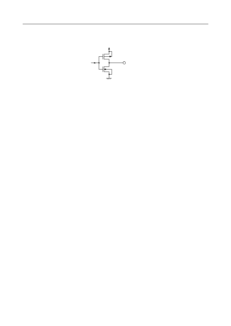
INPUT AND OUTPUT CONFIGURATION
Input pin
Input /Output pin
° Semiconductor
MSM6262-xx
4/52
From the inside of the device
CP, LOAD, DF, DO,
BUSY1 OUT, BUSY2 OUT
Applicable pins:
Output pin

° Semiconductor
MSM6262-xx
5/52
PIN CONFIGURATION (TOP VIEW)
1
2
3
4
5
6
7
8
9
10
11
12
13
14
15
16
17
18
19
20
21
22
23
24
64
63
62
61
60
59
58
57
56
55
54
53
52
51
50
49
48
47
46
45
44
43
42
41
25
26
27
28
29
30
31
32
33
34
35
36
37
38
39
40
80
79
78
77
76
75
74
73
72
71
70
69
68
67
66
65
COM 46
COM 47
COM 48
V
SS
(GND)
OSC1
OSC2
OSC3
TEST1
TEST2
TEST3
RESET
68 series/80 series
CS
E (RD)
R/W (WR)
A0
A1
DB
0
DB
1
DB
2
DB
3
DB
4
DB
5
DB
6
COM 29
COM 28
COM 27
COM 26
COM 25
COM 24
COM 23
COM 22
COM 21
COM 20
COM 19
COM 18
COM 17
COM 16
COM 15
COM 14
COM 13
COM 12
COM 11
COM 10
COM 9
COM 8
COM 7
COM 6
COM 45
COM 44
COM 43
COM 42
COM 41
COM 40
COM 39
COM 38
COM 37
COM 36
COM 35
COM 34
COM 33
COM 32
COM 31
COM 30
DB
7
BUSY 1 OUT
BUSY 2 OUT
DF
LOAD
CP
DO
V
DD
V
1
V
4
V
5
COM 1
COM 2
COM 3
COM 4
COM 5
80-Pin Plastic QFP
° Semiconductor
MSM6262-xx
6/52
PIN DESCRIPTIONS
Symbol
Type
OSC1
OSC2, OSC3
RESET
68 series/80 series
CS
R/W (WR)
E (RD)
A0, A1
DB
0
- DB
7
TEST1 - TEST3
V
DD
, V
SS
V
1
, V
4,
V
5
DO
CP
LOAD
DF
COM1 - COM48
BUSY1 OUT
BUSY2 OUT
I/O
I
I
I
I
I
I
I/O
I
O
O
O
O
O
O
O
Clock oscillating pins required for internal operation upon receipt
of the LCD drive signal and CPU instruction.
Reset pin
Selection pin for either 68 series CPU or 80 series CPU
Chip select pin. By setting CS at "L" level, MSM6262-xx
is set at selecting condition.
R/W pin of 68 series CPU shall be connected to this pin,
while WR pin shall be connected to this pin in the case of
80 series CPU.
E pin of 68 series CPU shall be connected to this pin,
while RD pin shall be connected to this pin in the case of
80 series CPU.
The address bus of CPU shall be connected to these pins.
Instruction code is set by these pins.
The data bus of CPU shall be connected to these pins. These
pins are used to set the data of the instruction or to read
the data.
Test pins. Normally these pins should be set at V
SS
or
open.
Voltage supply pins. V
DD
is also used for the common
bias voltage level to drive the LCD.
Common bias voltage input pins to drive the LCD
Serial data output pin for SEGMENT drivers
Clock pulse output pin. The clock output from this pin
enables the character pattern data, which is output from
DO, to input to the SEGMENT drivers (MSM5839C or MSM5259).
Load signal output pin. The character pattern data to
the SEGMENT drivers, which was output from DO and
CP, is loaded to the LCD output of the SEGMENT
drivers, synchronized with the COMMON signal.
B-type AC signal output pin to drive the LCD
COMMON signal output pins to drive the LCD
This pin shows the internal condition of MSM6262-xx.
"H" shows that MSM6262-xx is in internal operation,
while "L" shows that MSM6262-xx is ready to receive
the instruction from the CPU.
This pin shows that MSM6262-xx is in internal operation
based on the instruction from the CPU, or MSM6262-xx
is in display revising operation based on the instruction
from the CPU.
"H" shows that MSM6262-xx is in internal operation,
while "L" shows that the display on the LCD has been
established and the MSM6262-xx is ready to receive an
instruction.
Description
--
--

° Semiconductor
MSM6262-xx
7/52
ABSOLUTE MAXIMUM RATINGS
Parameter
Symbol
Condition
Rating
Unit
Applicable Pin
Supply Voltage
V
DD
Ta = 25∞C, V
DD
≠V
SS
V
≠0.3 to +7.0
V
DD,
V
SS
Supply Voltage
for Driving LCD
V
1
, V
4
, V
5
Ta = 25∞C
V
DD
≠ 12 to
V
DD
+ 0.3
V
V
1
, V
4
, V
5
Input Voltage
V
IN
Ta = 25∞C
≠0.3 to V
DD
+ 0.3
V
OSC1, RESET
68 series / 80 series
CS, A0, A1, R/W (WR)
E (RD), DB
0
- DB
7
Power Dissipation
P
D
Ta = 25∞C
500
mW
Storage Temperature
T
STG
≠≠
≠55 to +125
∞C
≠≠
≠≠
RECOMMENDED OPERATING CONDITOINS
Parameter
Symbol
Condition
Range
Unit
Applicable Pin
Supply Voltage
V
DD
V
4.5 to 5.5
V
DD,
GND
LCD Driving Voltage
V
LCD
1/5 bias, V
DD
≠V
5
3.0 to 11
V
Operating Temperature
∞C
≠≠
1/6, 1/7 bias, V
DD
≠V
5
4.0 to 11
1/8 bias, V
DD
≠V
5
4.5 to 11
V
V
V
DD,
V
1
, V
4
, V
5
≠20 to +75
≠≠
≠≠
Note: For bias, refer to *3 in the section "DC Characteristics".
T
op

° Semiconductor
MSM6262-xx
8/52
ELECTRICAL CHARACTERISTICS
DC Characteristics
*1.
This is applicable to the voltage drop which is caused between V
DD
, V
1
, V
4
, V
5
and COM1
- COM48 when a current of 50 mA is flowed in/out to/from all of COM1 - COM48. (When
the output level is either V
DD
or V
1
, it should be applied only when the current flows in.
When the output level is either V
4
or V
5
, it should be applied only when the current flows
in.
In this case, +5V is applied to V
DD
and V
1
, while ≠6 V is applied to V
4
and V
5
.)
*2.
This is applicable to the current which flows in to V
DD
under following conditions.
V
DD
= 5 V, V
SS
= 0 V, V
1
= 2.8 V, V
4
= -3.8 V, V
5
= ≠6 V, No load, No interface with CPU
*3.
V
1
to V
5
should be set at as follows.
Parameter
Symbol
Condition
Min.
Typ.
Max.
Unit
Applicable Pin
CS, R/W (WR)
E (RD), A0, A1
DB
0
- DB
7
DB
0
- DB
7
OSC1, RESET
68series/80series
DO, LOAD, DF
CP
BUSY1 OUT
BUSY2 OUT
I
O
= ± 50 mA
COM1 - COM48
CS, R/W (WR)
E (RD), A0, A1
OSC1, 68series/
80series
Supply Current
I
DD1
I
DD2
*2
*2
V
DD
(V
DD
= 4.5 to 5.5 V , Ta = ≠20 to +75∞C)
LCD Driving
Voltage
V
DD
≠V
5
V
1
, V
4
, V
5
RESET
"H" Input Voltage
"L" Input Voltage
"H" Output Voltage
"L" Output Voltage
"H" Input Voltage
"L" Input Voltage
"H" Output Voltage
"L" Output Voltage
"H" Output Voltage
"L" Output Voltage
"H" Output Voltage
"L" Output Voltage
V
IH1
V
IL1
V
OH1
V
OL1
V
IH2
V
IL2
V
OH2
V
OL2
V
OH3
V
OL3
V
OH4
COM Voltage Drop
"H" Input Current
"L" Input Current
"H" Input Current
V
OL4
V
COM
I
ILH1
I
ILL1
V
LCD
I
ILH2
I
ILL2
≠≠
≠≠
I
O
= ≠250 mA
I
O
= 1.8 mA
≠≠
≠≠
I
O
= ≠500 mA
I
O
= 500 mA
I
O
= ≠1 mA
I
O
= 1 mA
I
O
= ≠100 mA
I
O
= 1.6 mA
V
IN
= V
DD
V
IN
= V
SS
1/5 bias
1/6-1/7
bias
1/8 bias
V
IN
= V
DD
V
IN
= V
SS
,V
DD
= 5 V
2.2
≠0.3
2.4
≠≠
≠0.3
V
DD
≠0.8
0.85 V
DD
≠≠
0.85 V
DD
≠≠
2.4
≠≠
≠≠
≠≠
≠≠
≠≠
≠≠
3.0
4.0
4.5
≠≠
≠8
≠≠
≠≠
≠≠
≠≠
≠≠
≠≠
≠≠
≠≠
≠≠
≠≠
≠≠
≠≠
≠≠
≠≠
≠≠
≠≠
≠≠
≠≠
≠≠
≠≠
≠20
≠≠
V
DD
0.7
≠≠
0.4
V
DD
0.8
≠≠
0.15 V
DD
≠≠
0.15 V
DD
≠≠
0.4
2.9
1
≠1
1.5
1.5
11
11
11
2
≠60
V
V
V
V
V
V
V
V
V
V
V
V
mA
mA
mA
mA
V
V
V
mA
mA
"L" Input Current
*3
*1
V
DD
= 5 V,
f
OSC
= 500 kHz
(RC oscillation)
V
DD
= 5 V,
f
IN
= 500 kHz
(external oscillation)
V
° Semiconductor
MSM6262-xx
9/52
2 lines
4 lines
5 x 8
5 x 12
5 x 8
5 x 12
V
1
V
4
V
5
No. of lines
(N)
Pin
Font
configuration
V
DD
≠ ≠≠ V
LCD
V
DD
≠ ≠≠ V
LCD
V
DD
≠ V
LCD
1
5
4
5
V
DD
≠ ≠≠ V
LCD
V
DD
≠ ≠≠ V
LCD
V
DD
≠ V
LCD
1
6
5
6
V
DD
≠ ≠≠ V
LCD
V
DD
≠ ≠≠ V
LCD
V
DD
≠ V
LCD
1
7
6
7
V
DD
≠ ≠≠ V
LCD
V
DD
≠ ≠≠ V
LCD
V
DD
≠ V
LCD
1
8
7
8
V
LCD
= LCD driving voltage
AC Characteristics
*2
*3
*1
Open
Open
OSC3
OSC2
OSC1
Oscillation source
R
f
C
f
OSC3
OSC2
OSC1
R
f
= 39 kW ± 5%
C
f
= 22 pF ± 10%
(Keep the wiring from
OSC1, OSC2, and
OSC3 to R
f
and C
f
as short as possible.)
T
H
T
L
V
DD
≠0.8 V
0.5 V
DD
0.8 V
t
r
t
f
V
DD
≠0.8 V
0.5 V
DD
0.5 V
DD
0.8 V
f
DUTY
= ≠≠≠≠≠≠≠ x 100%
T
H
T
H
+ T
L
Parameter
Symbol
Condition
Min.
Typ.
Max.
Unit
Applicable Pin
(V
DD
= 4.5 to 5.5V , Ta = ≠20 to +75∞C)
V
IN
= V
SS
V
DD
= 5 V
OSC1, OSC2, OSC3
DB
0
- DB
7
V
IN
= V
DD
45
300
≠≠
Input Frequency
Input Clock Duty
Input Clock Rise Time
Input Clock Fall Time
RC Oscillation
Frequency
"H" Input Current
"L" Input Current
f
IN
f
DUTY
t
r
t
f
f
CR
I
ILH3
I
ILL3
*1, *2
*2
*2
*2
*3
≠≠
300
≠≠
≠45
OSC1
50
500
≠≠
≠≠
500
≠≠
≠120
55
700
100
100
700
1
≠250
%
kHz
ns
ns
kHz
mA
mA

° Semiconductor
MSM6262-xx
10/52
TIMING DIAGRAM
Interface with 80 Series CPU
(V
DD
= 4.5 to 5.5V, Ta = ≠20 to +75∞C)
Parameter
Symbol
Min.
Max.
Unit
Address Set-up Time
CS Set-up Time
WR "L" Pulse Width
RD "L" Pulse Width
WR, RD "H" Pulse Width
Address Hold Time
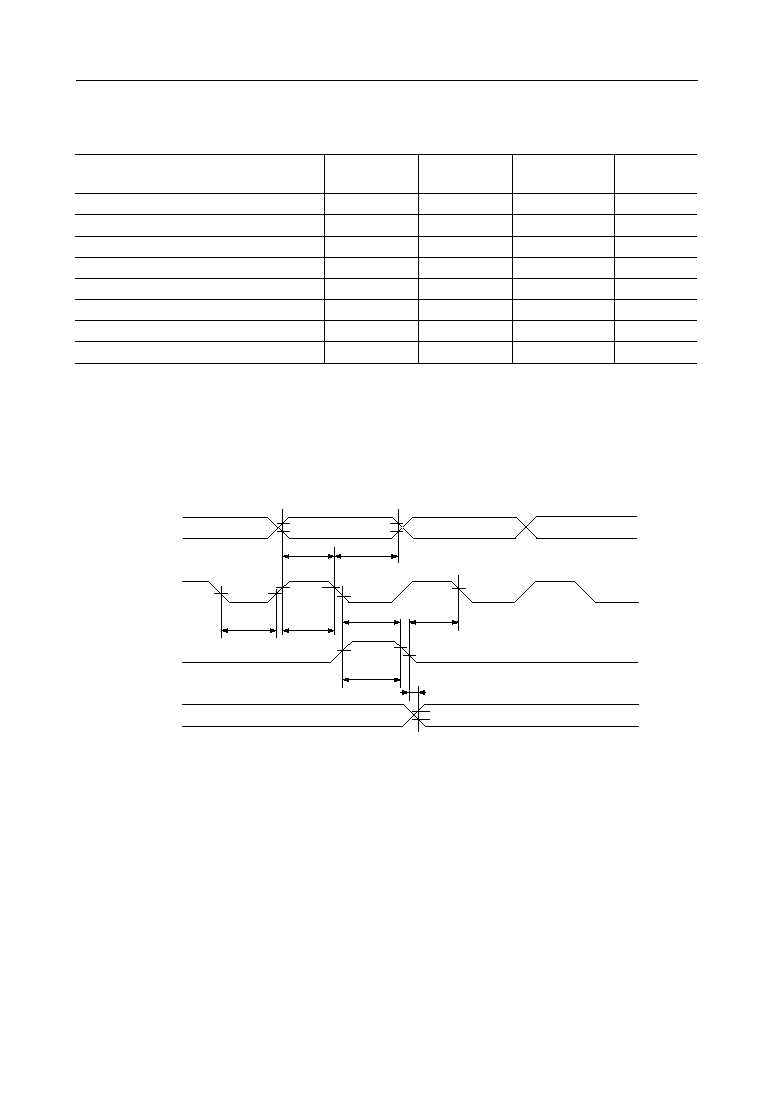
CS Hold Time
Data Set-up Time
Data Hold Time (Write operation)
WR, RD Fall Time
WR, RD Rise Time
Data Delay Time
Data Hold Time (Read operation)
Busy Output Delay Time
t
SA1
t
SA2
t
WWR
t
WRD
t
WH
t
HA1
t
HA2
t
SWD
t
HWD
t
f
t
r
t
SRD
t
HRD
t
BD
110
100
320
320
210
25
25
300
20
≠≠
≠≠
≠≠
0
≠≠
≠≠
≠≠
≠≠
≠≠
≠≠
≠≠
≠≠
≠≠
≠≠
25
25
190
≠≠
410
ns
ns
ns
ns
ns
ns
ns
ns
ns
ns
ns
ns
ns
ns
° Semiconductor
MSM6262-xx
11/52
Write operation
Read operation
A0,A1
V
IH
V
IL
V
IH
V
IL
CS
V
IL
V
IL
t
SA1
t
HA1
t
HA2
t
WRD
t
SA2
E (RD)
V
IH
V
IL
V
IH
t
WH
t
r
t
f
t
SRD
t
HRD
V
IH
V
IL
V
OH
V
OL
Valid data
DB0 - DB7
V
OH
V
OL
Refer to the DC Characteristics for the definition of V
IH
, V
IL
, V
OH
and V
OL
.
A0,A1
V
IH
V
IL
V
IH
V
IL
CS
V
IL
V
IL
t
SA1
t
HA1
t
HA2
t
W WR
t
SA2
R/W (WR)
V
IH
V
IL
V
IH
t
WH
t
r
t
f
t
SWD
t
HWD
V
IH
V
IL
V
IH
V
IL
V
IH
V
IL
t
BD
V
OH
Valid data
DB0 - DB7
BUSY 1 OUT, BUSY 2 OUT
° Semiconductor
MSM6262-xx
12/52
Z80
MSM6262-xx
A
0
- A
15
WR
DB
0
- DB
7
DB
0
- DB
7
A0, A1
CS
R/W (WR)
E (RD)
68 series/80 series
V
SS
Address
Decoder
* A pull-up resistor of about 50 kW is required when the output of CPU becomes high impedance.
*
*
*
RD
*
IORQ
*
∑ Interface with Z80

° Semiconductor
MSM6262-xx
13/52
∑ Interface with 80C49
∑ Interface with 80C51
MSM80C49
MSM6262-xx
WR
DB
0
- DB
7
DB
0
- DB
7
A0, A1
CS
R/W (WR)
E (RD)
68 series/80 series
V
SS
Address
Decoder
* A pull-up resistor of about 50 kW is required when the output of CPU becomes high impedance.
*
RD
*
*
STB
8282
ALE
P20
- P22
*
MSM80C51
MSM6262-xx
WR
P00
- P07
DB
0
- DB
7
A0, A1
CS
R/W (WR)
E (RD)
68 series/80 series
V
SS
Address
Decoder
* A pull-up resistor of about 50 kW is required when the output of CPU becomes high impedance.
*
RD
*
STB
8282
ALE
P20
- P22
*
*
° Semiconductor
MSM6262-xx
14/52
Interface with 68 Series CPU
(V
DD
= 4.5 to 5.5 V, Ta = ≠20 to +75∞C)
Parameter
Symbol
Min.
Max.
Unit
Cycle Time
Address, R/W Set-up Time
CS Set-up Time
E signal "H" Pulse Width
E signal "L" Pulse Width
Address, R/W Hold Time
CS Hold Time
Data Set-up Time
Data Hold Time (Write operation)
E signal Rise Time
E signal Fall Time
Data Delay Time
Data Hold Time (Read operation)
Busy Output Delay Time
t
C
t
B1
t
B2
t
W
t
L
t
A1
t
A2
t
I
t
H
t
r
t
f
t
D
t
O
t
BD
500
100
90
220
210
20
20
225
30
≠≠
≠≠
≠≠
10
≠≠
≠≠
≠≠
≠≠
≠≠
≠≠
≠≠
≠≠
≠≠
≠≠
25
25
180
≠≠
410
ns
ns
ns
ns
ns
ns
ns
ns
ns
ns
ns
ns
ns
ns
° Semiconductor
MSM6262-xx
15/52
Read operation
A0, A1
R/W (WR)
E (RD)
DB0 - DB7
CS
V
IH
V
IL
V
IH
V
IL
t
B1
t
A1
V
IH
V
IH
t
W
t
L
V
IH
V
IL
V
IL
V
IH
V
IL
t
r
t
f
t
O
V
OH
V
OL
Valid data
t
A2
t
B2
V
IL
V
IL
t
C
V
OH
V
OL
t
D
Refer to the DC Characteristics for the definition of V
IH
, V
IL
, V
OH
, and V
OL
.
Write operation
A0, A1
R/W (WR)
E (RD)
DB0 - DB7
CS
Busy 1 OUT, Busy 2 OUT
V
IH
V
IL
V
IH
V
IL
t
B1
t
A1
V
IL
V
IL
t
W
t
L
V
IH
V
IL
V
IL
V
IH
V
IL
t
r
t
f
t
I
t
H
V
IH
V
IL
V
IH
V
IL
Valid data
t
A2
t
B2
V
IL
V
IL
t
C
t
BD
V
OH

° Semiconductor
MSM6262-xx
16/52
6809
MSM6262-xx
A
0
- A
15
E
R/W
O
DB
0
- DB
7
DB
0
- DB
7
A0, A1
CS
R/W(WR)
E (RD)
68 series/80 series
V
DD
Address
decoder
* A pull-up resistor of about 50 kW is required when the output of CPU becomes high impedance.
*
*
*
*
∑ Interface with 6809
° Semiconductor
MSM6262-xx
17/52
Interface with Segment Driver
DO
CP
LOAD
DF
V
OH
V
OL
V
OH
V
OL
V
OH
V
OL
V
OL
V
OH
V
OH
t
SETUP
t
HOLD
V
OH
V
OH
V
OL
V
OH
V
OL
t
LW(CP)
T
HW(CP)
t
CL
t
LC
t
M
t
HW
(L)
Refer to the DC Characteristics for the definition of V
IH
, V
IL
, V
OH
, and V
OL
.
(V
DD
= 4.5 to 5.5 V, Ta = ≠20 to +75∞C, f
OSC
= 500 kHz)
Parameter
Symbol
Min.
Max.
Unit
Clock "L" Pulse Width
Clock "H" Pulse Width
Do Set-up Time
Do Hold Time
LOAD, Clock Set-up Time
LOAD, Clock Hold Time
LOAD, "H" Pulse Width
DF Delay Time
t
LW(CP)
400
--
ns
t
HW(CP)
400
--
ns
t
SETUP
200
--
ns
t
HOLD
200
--
ns
t
CL
200
--
ns
t
LC
100
--
ns
t
HW(L)
400
--
ns
t
M
≠500
500
ns
° Semiconductor
MSM6262-xx
18/52
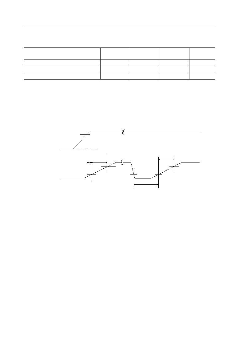
Reset Waveform
V
DD
RESET
4.5 V
0 V
t
RR1
t
RR2
t
RR2
V
IL
V
IH
V
IL
V
IL
V
IH
t
RLW
Refer to the DC Characteristics for the definition of V
IH
, V
IL
, V
OH
, and V
OL
.
(V
DD
= 4.5 to 5.5 V, Ta = ≠20 to +75∞C)
Parameter
Symbol
Min.
Max.
Unit
"L" Input Time upon power on
"L" Input Width when in operation
Rise Time
t
RR1
0.25
≠≠
ms
t
RLW
0.5
≠≠
ms
t
RR2
0.1
200
ms

° Semiconductor
MSM6262-xx
19/52
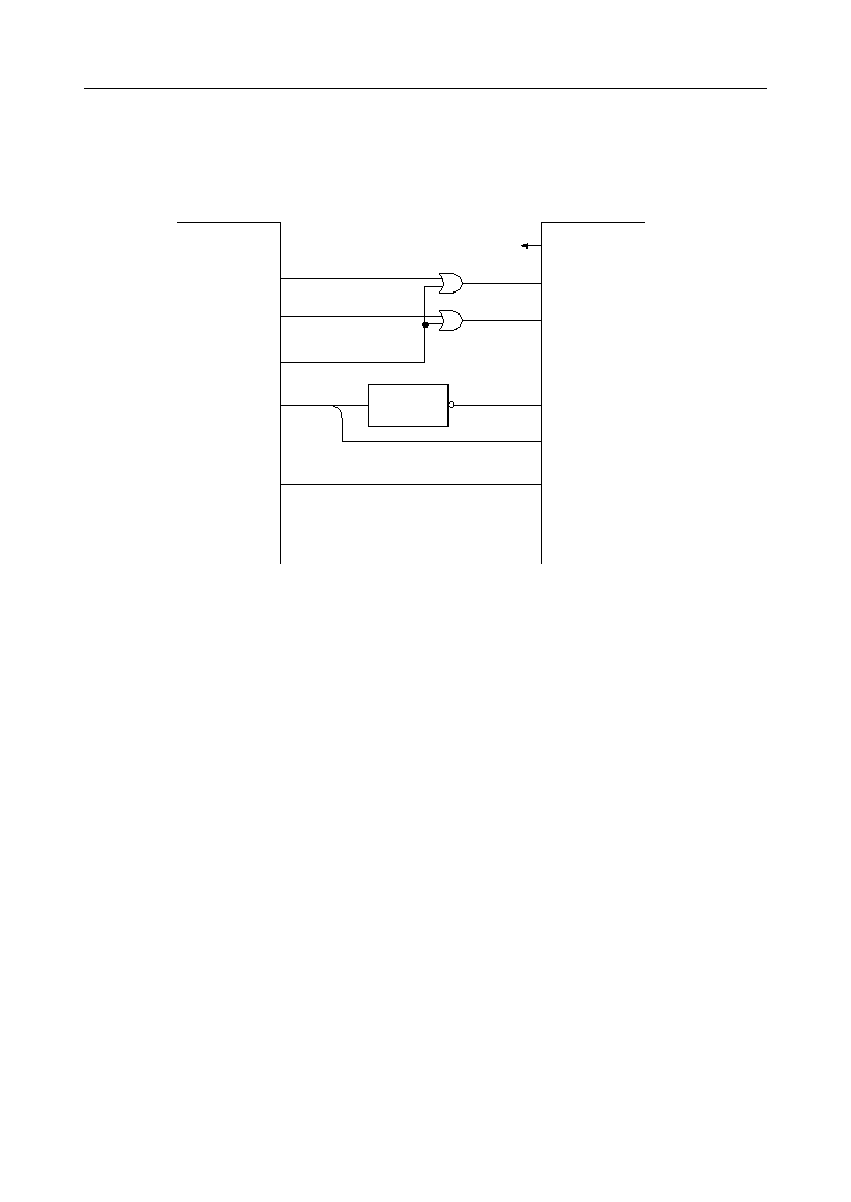
FUNCTIONAL DESCRIPTION
1. Instruction Register (IR) and Data Register (DR)
The MSM6262-xx has two registers, instruction register (IR) and data register (DR).
IR is used to store the address code or instruction code of display data RAM (DD RAM) or
character generator RAM (CG RAM).
This register can be written by the CPU, but cannot be read out by the CPU.
DR is used to store the data to write into (or read out) the data to/from DD RAM or CG RAM.
The data written into DR by the CPU is automatically written into the DD RAM or CG RAM.
When an address code is written into IR, the data of the specified address is automatically
transferred to the DR from either DD RAM or CG RAM. By having the CPU subsequently read
the DR, it is possible to verify DD RAM or CG RAM data.
After the writing of DR by the CPU, the DD RAM or CG RAM of the next address is selected
to be ready for the next CPU writing.
Likewise, after the reading operation of the CPU, DD RAM or CG RAM data of the next
address is transferred to the DR, when CPU is ready for the next reading operation.
2. Busy Flag (BF)
When the output of BUSY 1 OUT is "H", MSM6262-xx is engaged in internal operation.
When the output of BUSY 2 OUT is "H", it indicates that MSM6262-xx is engaged in internal
operation or MSM6262-xx is engaged in the revising of the display starting line on the LCD.
(Refer to the instruction table.)
When the output of BUSY 1 OUT is "H", any input of new instruction is ignored. So, before
setting a new instruction, it is necessary to check whether BUSY 1 OUT and BUSY 2 OUT are
at "L".
3. Address Counter (ADC)
The address counter (ADC) allocates the address for the DD RAM and CG RAM write/read
and also for the cursor display.
When the instruction code for a DD RAM address or CG RAM address setting is input to IR,
after deciding whether it is DD RAM or CG RAM, the address counter code is transferred from
IR to ADC. After writing (reading) the display data to (from) the DD RAM or CG RAM, the
ADC increments (or decrements) by 1 automatically as its internal operation.
° Semiconductor
MSM6262-xx
20/52
4. Timing Generator Circuit
This circuit generates the timing signal for the internal operation by CPU's instruction as well
as to operate the internal circuit of DD RAM, CG RAM, CG ROM and so forth. It also generates
the transfer signal to the SEGMENT driver (MSM5839C or MSM5259).
The internal operation accessed by the CPU and internal operation for LCD display is
independent.
So, a manipulation such as writing data from CPU to DD RAM will not have an influence such
as display flickering upon any part other than the display part to which the data is written.
5. Display Data RAM (DD RAM)
DD RAM is used to store the 8-bit character code (refer to Table 1) and 1-bit under-line data.
The address of DD RAM corresponds to the display position on the LCD. The correspondence
is described below.
DD RAM address (set to ADC) is described as hexadecimal.
(1) Relation between DD RAM and display position in 2-line display mode
1
2
3
4
5
≠ ≠ ≠
79
80
≠ ≠ ≠
≠ ≠ ≠
00
80
01
81
02
82
03
83
04
84
4E
CE
4F
CF
1st line
2nd line
Digit
Display position
DD RAM address
(hexadecimal)
1st line
2nd line
00
80
1
2
3
4
5
6
7
8
9
10 11
12 13
14 15 16
01
81
02
82
03
83
04
84
05
85
06
86
07
87
08
88
09
89
0A
8A
0B
8B
0C
8C
0D
8D
0E
8E
0F
8F
Digit
MSM5839C (2)
MSM5259 (2) }
MSM5839C (1)
MSM5259 (1)
{ or
Note: The address of the last digit of the first line and the first digit of the second line
does not have any continuity.
DB
7
DB
6
DB
5
DB
4
DB
3
DB
2
DB
1
DB
0
MSB
LSB
Hexadecimal
Hexadecimal
Example: When DD RAM address is 3A
3
A
L
L
L
H
H
H
L
H
ADC
(2) When 2 pieces of MSM5389C(or MSM5259) are connected to MSM6262-xx, 32
characters can be displayed from the first digit to yhe 16th degit.
° Semiconductor
MSM6262-xx
21/52
When the display is shifted by an instruction, the relation between the DD RAM address and
the display position becomes as follows.
(4) Relation between the DD RAM and display position in 4-line display mode
1st line
2nd line
4F
CF
1
2
3
4
5
6
7
8
9
10
11
12
13
14
15
16
00
80
01
81
02
82
03
83
04
84
05
85
06
86
07
87
08
88
09
89
0A
8A
0B
8B
0C
8C
0D
8D
0E
8E
Digit
MSM5839C (2)
MSM5259 (2) }
MSM5839C (1)
MSM5259 (1)
{ or
1st line
2nd line
01
81
02
82
03
83
04
84
05
85
06
86
07
87
08
88
09
89
0A
8A
0B
8B
0C
8C
0D
8D
0E
8E
0F
8F
10
90
(Shift to the left)
(Shift to the right)
1st line
2nd line
Digit
MSM5839C (2)
MSM5259 (2)
MSM5839C (1)
MSM5259 (1)
{ or
00
80
1
2
3
4
5
6
7
8
9
10
11 12
13 14
15 16
17 18
≠ ≠ ≠
73 74
75 76 77 78
79 80
01
81
02
82
03
83
04
84
05
85
06
86
07
87
08
88
09
89
0A
8A
0B
8B
0C
8C
0D
8D
0E
8E
0F
8F
10
90
11
91
48
C8
49
C9
4A
CA
4B
CB
4C
CC
4D
CD
4E
CE
4F
CF
≠ ≠ ≠
≠ ≠ ≠
MSM5839C (3)-(9)
MSM5259 (3)-(9)
MSM5839C (10)
MSM5259 (10) }
1st line
2nd line
Digit
Display position
DD RAM address
(hexadecimal)
Note: The address of the last digit of the previous line and the first digit of the
next line does not have any continuity.
3rd line
4th line
1
2
3
4
5
39
40
00
40
80
C0
01
41
81
C1
02
42
82
C2
03
43
83
C3
04
44
84
C4
26
66
A6
E6
27
67
A7
E7
≠ ≠ ≠
≠ ≠ ≠
≠ ≠ ≠
≠ ≠ ≠
≠ ≠ ≠
(3) The maximum DD RAM capacity of MSM6262-xx is for 160 characters. So, up to 10 pieces
of MSM5839C (or MSM5259) can be connected in the case of 2-line display mode.

° Semiconductor
MSM6262-xx
22/52
When the display is shifted by an instruction, the relation between the DD RAM address and
the display position becomes as follows.
1
2
3
4
5
6
7
8
9
10
11 12 13 14 15 16 17
18
≠ ≠ ≠
33 34 35 36
37 38 39
40
00
01 02 03 04
05 06
07 08 09
0A 0B 0C 0D 0E 0F
10
11
≠ ≠ ≠
20
21 22 23
24 25
26
27
41 42 43 44
45 46
47 48 49
4A 4B 4C 4D 4E 4F
50
51
≠ ≠ ≠
60
81 82 83 84
85 86
87 88 89
8A 8B 8C 8D 8E 8F
90
91
≠ ≠ ≠
A0
C1 C2 C3 C4
C5 C6
C7 C8 C9 CA CB CC CD CE CF
D0
D1
≠ ≠ ≠
E0
40
80
C0
61
A1
E1
62
A2
E2
63
A3
E3
64
A4
E4
65
A5
E5
66
A6
E6
67
A7
E7
1st line
Digit
2nd line
3rd line
4th line
MSM5839C (1)
MSM5259 (1)
or
MSM5839C (2)
MSM5259 (2)
MSM5839C (3),(4)
MSM5259 (3),(4)
MSM5839C (5)
MSM5259 (5)
1st line
2nd line
00
40
1
2
3
4
5
6
7
8
9
10
11
12
13
14
15
16
01
41
02
42
03
43
04
44
05
45
06
46
07
47
08
48
09
49
0A
4A
0B
4B
0C
4C
0D
4D
0E
4E
0F
4F
Digit
MSM5839C (2)
MSM5259 (2) }
MSM5839C (1)
MSM5259 (1)
{ or
3rd line
4th line
80
C0
81
C1
82
C2
83
C3
84
C4
85
C5
86
C6
87
C7
88
C8
89
C9
8A
CA
8B
CB
8C
CC
8D
CD
8E
CB
8F
CF
(6) The maximum DD RAM capacity of MSM6262-xx is for 160 characters. So, up to 5pieces
of MSM5839C (or MSM5259) can be connected in the case of 4-line display mode.
(5) When 2 pieces of MSM5839C (or MSM5259) are connected to MSM6262-xx, 64 characters
can be displayed from the first digit to the 16th digit.
1st line
2nd line
27
67
1
2
3
4
5
6
7
8
9
10
11
12
13
14
15
16
00
40
01
41
02
42
03
43
04
44
05
45
06
46
07
47
08
48
09
49
0A
4A
0B
4B
0C
4C
0D
4D
0E
4E
Digit
MSM5839C (2)
MSM5259 (2) }
MSM5839C (1)
MSM5259 (1)
3rd line
4th line
E7
A7
C0
80
C1
81
C2
82
C3
83
C4
84
C5
85
C6
86
C7
87
C8
88
C9
89
CA
8A
CB
8B
CC
8C
CD
8D
CE
(shift to right direction)
1st line
2nd line
01
41
02
42
03
43
04
44
05
45
06
46
07
47
08
48
09
49
0A
4A
0B
4B
0C
4C
0D
4D
0E
4E
0F
4F
10
50
3rd line
4th line
81
C1
82
C2
83
C3
84
C4
85
C5
86
C6
87
C7
88
C8
89
C9
8A
CA
8B
CB
8C
CC
8D
CD
8E
CE
8F
CF
90
D0
(shift to left direction)
8E
{ or

° Semiconductor
MSM6262-xx
23/52
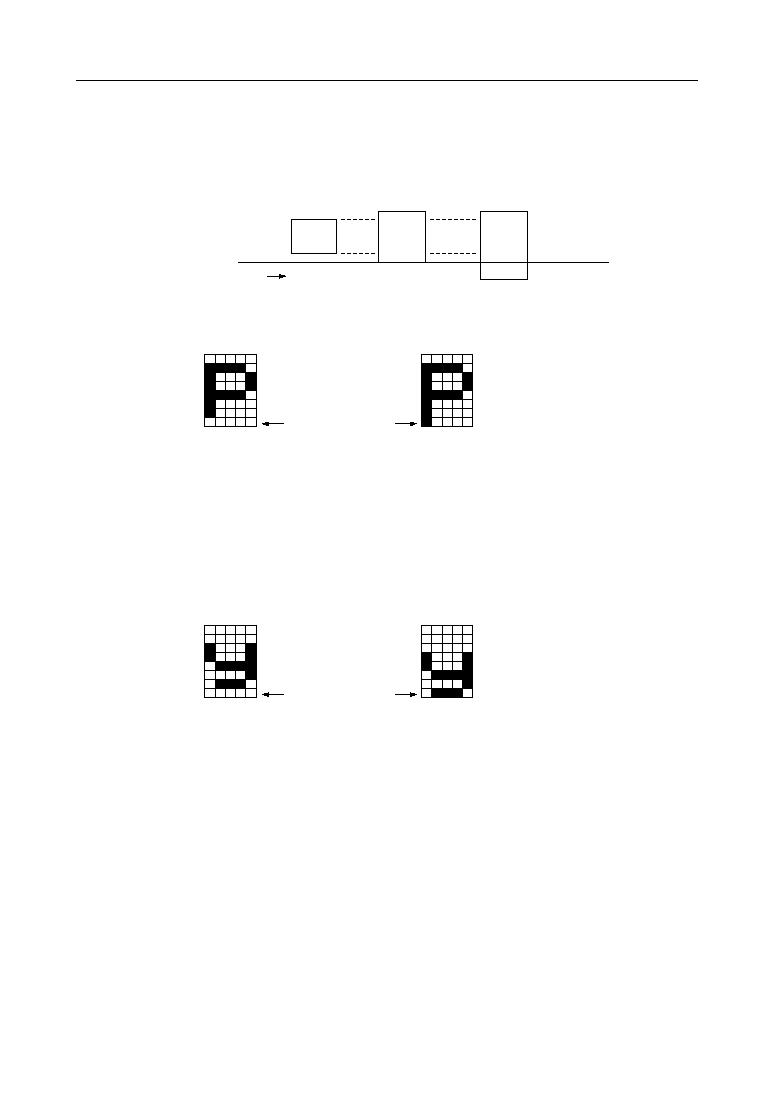
6. Cursor/Blink Control Circuit
This is the circuit to control the generation of cursor and its blinking. This circuit is controlled
by the program of the CPU.
The position of the cursor and its blink appears on the position according to the ADC contents,
which correspond to the address of DD RAM. For example, when the ADC is set as "07" (hex.),
the position of cursor and its blinking becomes as follows.
7. Underline Control Circuit
First, either underline display mode or underline blinking mode has to be set by the CPU.
When an instruction to enable the underline function is input from the CPU, the cursor
display shifts to the right direction (increment) or left direction (decrement). Display of
underline appears (or disappears) on the same position where cursor was displayed.
An input of "H" data enables the underline display, while an input of "L" data deletes the
underline.
8. Character Generator ROM (CG ROM)
CG ROM stores the character pattern. MSM6262-xx has 128 kinds of 5 x 7-dot patterns, 96
kinds of 5 x 11-dot patterns and 32 kinds of 5 x 12-dot patterns. The character pattern
corresponds to the character code which is written into the DD RAM.
The relation between 8-bit character code and character pattern is described in Table 1.
When the 8-bit character code of CG ROM is written into the DD RAM, the character pattern
of the corresponding character code of the CG ROM is displayed on the LCD position
corresponding to the DD RAM address.
When all of the upper 4 bits of CG ROM code are "L", CG ROM can be switched to CG RAM.
DB7
DB0
ADC
0
0
0
0
0
1
1
1
0
7
≠ ≠ ≠
00
80
01
81
02
82
03
83
04
84
05
85
06
86
07
87
08
88
--
1
2
3
4
6
7
8
9
5
Digit
Cursor and its blinking position
79
80
≠ ≠ ≠
≠ ≠ ≠
4E
CE
4F
CF
2-line display
1
2
3
4
6
7
8
9
5
Digit
Cursor and its blinking position
4-line display
00
01
02
03
04
05
06
07
08
--
40
80
C0
41
81
C1
42
82
C2
43
83
C3
44
84
C4
45
85
C5
47
87
C7
46
86
C6
48
88
C8
≠ ≠ ≠
≠ ≠ ≠
≠ ≠ ≠
≠ ≠ ≠
≠ ≠ ≠
39
40
26
27
66
67
A6
A7
E6
E7
Note: Cursor display and blinking can be performed even when the CG RAM address is
set in the ADC. So, it is necessary to disable the cursor display and blinking when
the CG RAM address is set in the ADC.

° Semiconductor
MSM6262-xx
24/52
Table 1 Character code and character pattern of Standard Code (MSM6262-04)

° Semiconductor
MSM6262-xx
25/52
9. Character Generator RAM (CG RAM)
The CG RAM is used to display user's original character pattern other than CG ROM.
The CG RAM has capacity (32 bytes = 256 bits) to write 4 kinds of 5 x 8 dots and 2 kinds of 5
x 12 dots.
In displaying the character pattern stored in the CG RAM, CG RAM has to be enabled by an
instruction. When CG RAM is enabled, CG ROM code for 16 characters cannot be read out
since the CGROM code with all "L" on the upper 4 bits is used as CG RAM code.
The following describes how to write character patterns into the CG RAM and how to display
them on the LCD.
(1) When the character pattern is 5 x 8 dots (See Table 2-1)
∑ A method to write character pattern into the CG RAM by the CPU
The lower 3 bits (0 - 2) of the CG RAM address correspond to the line position of the
character pattern. The upper 2 bits (3, 4) of the CG RAM address correspond to the lower
2 bits (0, 1) of the character code.
First, set increment of decrement by the CPU, and then input CG RAM address. After this,
write character pattern data into CG RAM through DB0 to DB7 line by line.
DB0 - DB7 correspond to CG RAM data 0 - 7 in Table 2-1.
Display is turned on when "H" is set as input data and turned off when "L" is set as input
data.
Since the ADC is automatically incremented or decremented by 1 after the writing of data
to the CG RAM, it is not necessary to set the CG RAM address again.
To enable cursor display, set all input data on the line where the lower 3 bits of the CG RAM
(0-2) are all "H" to "L".
0 - 4 bits of CG RAM data are output to the LCD as the display data; however, 5 - 7 bits of
CG RAM data are not. But it can be used as the data RAM because the data can be written/
read through DB0 to DB7.
∑ A method to display the CG RAM character pattern to the LCD
First, an instruction to enable the CG RAM has to be input from the CPU. CG RAM is
selected only when all of the upper 4 bits of the character code is "L".
So, the character pattern of CG RAM is displayed on the LCD position that corresponds to
the DD RAM address, when the character code shown in Table 2-1 is written into DD RAM.
Since the bits 2 and 3 of the character code are regarded as invalid, "K" is displayed when
the character codes "01", "05", "'09", and "0D" are selected.
(2) When the character pattern is 5 x 12 dots (See Table 2-2)
∑ A method to write character pattern into the CG RAM by the CPU
The lower 4 bits of CG RAM address (0 - 3) correspond to the line position of the character
pattern.
The upper 1 bit of CG RAM address bit 4 corresponds to the bit 1 of the character code.
First, set increment or decrement by the CPU, and then input CG RAM address.
After this, write the character pattern data into CG RAM through DB
0
to DB
7
line by line.
DB
0
- DB
7
correspond to CG RAM data 0 - 7 in Table 2-2.
Display is turned on when "H" is set as the input data and turned off when "L" is set

° Semiconductor
MSM6262-xx
26/52
as the input data.
Since the ADC is automatically incremented or decremented by 1 after the writing of data
to the CG RAM, it is not necessary to set the CG RAM address again.
To enable cursor display, set all input data on the line where the CG RAM address is "0B"
or "1B" (hex.) to "L".
The addresses "0" to "B" (hexadecimal) in the bits 0 to 4 of the CG RAM data are output on
the LCD as the display data. However, the addresses "C" to "F" (hexadecimal) in the bits
0 to 4, and 5 to 7 of the CG RAM data are not output on the LCD. But these CG RAM data
can be used as the data RAM so that they can be written into or read out through DB0 to
DB7.
∑ A method to display the CG RAM character pattern on the LCD
First, an instruction to enable the CG RAM has to be input from the CPU. CG RAM is
selected only when all of the upper 4 bits of the character code is "L".
So, the character pattern of CG RAM is displayed on the LCD position corresponding to
the DD RAM address, when the character code shown in Table 2-2 is written into the DD
RAM.
Since bits 0, 2 and 3 of the character code are regarded as invalid, the character of "m" is
displayed when the character codes "00", "01", "04", "05", "08", "09", "0C" and "0D" are
selected.
(3) A method to read out the CG RAM data
First, set the CG RAM address by inputting a CG RAM address set instruction from the
CPU.
Then, execute the CG RAM/DD RAM data read instruction. The set data of CG RAM
address is output from the DB0 to DB7. The 8-bit data, read out from the MSM6262-xx,
corresponds to the data which is written into the CG RAM. Since the CG RAM address is
automatically incremented or decremented by 1, the CG RAM read out instruction c a n
be successfully input. It is necessary, however, to set the DD RAM at data transferring
condition by executing the DD RAM address set instruction after all of CG RAM data are
read out.
° Semiconductor
MSM6262-xx
27/52
CG RAM DATA
(Character Pattern )
DD RAM DATA
CG RAM
ADDRESS
(Character Code )
7 6 5 4 3 2 1 0
L L L L L
7 6 5 4 3 2 1 0
LSB MSB
LSB MSB
LSB
L
L
L
H
H
H
H
X X X L H H H L
H
H
L L L L X X L L
H
H
L
L
4 3 2 1 0
H
L H L L L
L
L
L
H
H
H
H
X X X H L L L H
L L L L X X L H
H H L L L
L
L
L
H
H
H
H
X X X L H H H L
L L L L X X H H
X: Don't care
L H
H L
H H
L L
L H
H L
H H
L H
H L
H H
L L
L H
H L
H H
L
H
H
L
L
H
H
H
L
H
L
H
L
H
L L
H
L
L L
H
L
L L
H
L
L L
H
L
L L
H
L
H H
L
H
L L
L
L
H
H
H
H
H
L
H
L H
L
L
L L
L
H
H L
L
L
L L
L
H
L H
L
L
L L
L
L L
L
L
H
L
L
L
L
L
L
L
L L
L
H
L L
L
H
L L
L
H
L L
L
H
L L
L
H
H H
H
L L
L
L
L
Table 2-1 Relation between CG RAM data (character pattern) vs. CGRAM
address and DDRAM data vs. character pattern when the character
pattern is 5
•
•
•
•
• 8 dots.
° Semiconductor
MSM6262-xx
28/52
Table 2-2 Relation between CGRAM data (character pattern) vs. CGRAM address
and DDRAM data vs. character pattern when the character pattern
is 5
•
•
•
•
• 12 dots.
7 6 5 4 3 2 1 0
L
7 6 5 4 3 2 1 0
LSB MSB
LSB MSB
LSB
L
L
L
H
H
H
H
X X X
L
L
L
L
L
4 3 2 1 0
L
L
L
L
L
H
H
H
H
L
L
L
H
H
H
H
X X X
L L L L X X H
X: Don't care
L H
H L
H H
L L
L H
H L
H H
L L
L H
H L
H H
L L
L H
H L
L
H
H
L
L
H
H
H
L
H
L
H
L
H
L L
L
L
L L
L
L
H L
L
L
H H
H
H
L H
L
L
H H
H
H
H
H L
L
H
L
L
L
H H
H
H
L H
L
L
L L
L
L
L L
L
L
L
L
L
H
H
L
L
L L
L
L
L L
L
L
L L
L
L
L L
L
L
L L
H
L
L L
L
H H
L
L
H
H H H
L
L
L
L
L
H
L
H
L
L
L
H
L L
L
H
H L
L
L L
L
L
L
L H H
L L L
L
L
H
H
H
H
L
L
H
H
L
H
L
H
X X X
X
X
L
L
L
L
L
L
L
H
H
H
H
H
H
H
H
L
L
L
L
L
L
L
H
H
H
H
H
H
H
H
L L L
L
L
L L L
L
L L L
L
L L L
L
L
X
L L L L X X L X
CG RAM DATA
(Character Pattern)
DD RAM DATA
CG RAM
ADDRESS
(Character Code)
H
X X X
X
X
B
B

° Semiconductor
MSM6262-xx
29/52
9. LCD Display Circuit (COM1 to COM48, DO, CP, LOAD, DF)
The MSM6262-xx is provided with COMMON signal output. So, maximum 160 characters
can be displayed when it is used together with SEGMENT drivers (MSM5259 or MSM5839C).
Interface between MSM6262-xx and SEGMENT drivers can be done by using DO, CP, LOAD
and DF.
The SEGMENT data is serially output from DO pin, synchronized with the pulse which is
output from the CP pin.
This data, input to the SEGMENT driver, is converted from serial data to parallel data by the
latch pulse which is output from the LOAD pin of MSM6262-xx and this converted data is
used as the display data. This parallel/serial conversion is performed synchronized with the
COMMON signal of MSM6262-xx and LCD display AC signal which is output from DF pin.
So, this signal can drive dot matrix LCD panel.
10. Reset Circuit
Power-on-reset is required for MSM6262-xx when it is powered-on. So, a capacitor has to be
connected between RESET pin and V
SS
pin.
It is also advisable to connect a diode between RESET pin and V
DD
pin when it is required to
connect a capacitor of more than 3.3
µ
F to RESET pin.
When the power-on reset circuit normally operates, the busy flags 1 and 2 become at "H" level
for about 10 ms after the power-on. During this period, a initialization of MSM6262-xx is
performed by following procedures.
1 Display is cleared
2 CG ROM becomes enabled
3 No display shift
4 ADC is incremented
5 2-line display mode
6 5 x 8 dots font configuration
7 No display shift for "g", "j", "p", "q" and "y"
8 Display off
9 No display of cursor, blinking and underline
11. Data Bus with CPU
MSM6262-xx can be interfaced with 8-bit CPU, such as 6809, Z80, 80C49 and 80C51. When
MSM6262-xx is connected with 6809, the 68 series/80 series pin has to be connected to V
DD
.
When MSM6262-xx is connected with Z80, 80C49 or 80C51, the 68 series/80 series pin has to
be connected to V
SS
. The level at 68 series/80 series cannot be switched during MSM6262-xx's
operation. It must be connected with either V
DD
or V
SS
before MSM6262-xx is turned on.
Note: It is possible, indeed, to change the 68 series/ 80 series pin's level when a reset signal
is being input to RESET pin. However, the 68 series /80 series pin does not have
characteristics to have an interface with MCU, nor does it have an antichattering
circuit.
Further, if a reset signal is input, the MSM6262-xx is initialized as described above.
So, in this case, changing the 68 series/80 series pin level is not recommended.
° Semiconductor
MSM6262-xx
30/52
80 series CPU data transfer
,
,,
,
,
,
,,
,
,,
,
,
,
,,
,
,
,
E (RD)
R/W (WR)
A
1
A
0
DB
7
DB
6
DB
5
DB
4
DB
3
DB
2
DB
1
DB
0
BUSY1
(Internal
operation)
BUSY2
(Internal
operation)
Write an instruction (IR)
Read the busy flag
* : Don't care
Write the data register (RD)
IR
7
IR
6
IR
5
IR
4
IR
3
IR
2
IR
1
IR
0
BUSY1
BUSY2
*
*
*
*
*
*
NO BUSY1
NO BUSY2
CG/DD
I/D
S
A/O
D
UD
DR
7
DR
6
DR
5
DR
4
DR
3
DR
2
DR
1
DR
0
,
,
,
,,
,

° Semiconductor
MSM6262-xx
31/52
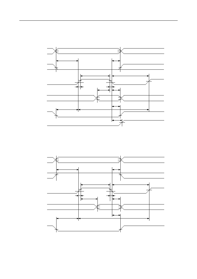
68 series CPU data transfer
,,
,
,
,
,
,
,
,
,
,
,
,
,
,
,
,
,
,
,
,
,
,
,
,
,
,
A
1
A
0
DB
7
DB
6
DB
5
DB
4
DB
3
DB
2
DB
1
DB
0
BUSY1
(Internal
operation)
BUSY2
(Internal
operation)
Write an instruction (IR)
Read the busy flag
* : Don't care
Write the data register (RD)
IR
7
IR
6
IR
5
IR
4
IR
3
IR
2
IR
1
IR
0
BUSY1
BUSY2
*
*
*
*
*
*
NO BUSY1
NO BUSY2
CG/DD
I/D
S
A/O
D
UD
DR
7
DR
6
DR
5
DR
4
DR
3
DR
2
DR
1
DR
0
E (RD)
R/W (WR)
,
,
° Semiconductor
MSM6262-xx
32/52
Instruction Table
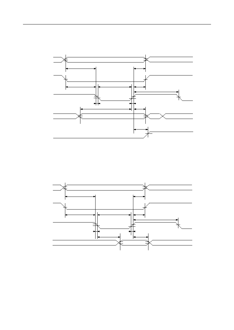
80series CPU
68series CPU
Note
1
R/W
A
1
A
0
DB
0
Explanation
Execution Time (MAX),
When fosc = 500kHz
DB
1
DB
2
DB
3
DB
4
DB
5
DB
6
DB
7
DB
0
DB
1
DB
2
DB
3
DB
4
DB
5
DB
6
DB
7
A
1
A
0
Display Clear
Return
Under Line
Entry Mode Set
Display/Cursor Shift
CG RAM address Set
Function Set
Display Control
CG RAM/DD RAM
Data Write
DD RAM Address
Set
Read the Underlined
Data
Read the CG RAM/
DD RAM Data
Read the Address
Counter Content
Read Busy Flag
L
L
L
L
L
L
L
L
L
L
H
H
H
H
L
L
L
L
L
L
L
L
L
H
L
L
H
H
L
L
L
L
L
L
L
L
H
L
L
H
L
H
L
L
L
L
L
L
L
H
ULD
B1F
L
L
L
L
L
L
H
D
B2F
CG/
DD
I/D
S
A/O
D
UD
L
L
L
L
L
H
N
C
L
L
L
L
H
*
B
L
L
L
H
S/C
F
1
UC
L
L
H
I/D
UD/
RL
F
2
UB
L
H
UL
S
D
2
UR/
DL
F
3
*
H
CR/C
*
A/O
D
1
( )
*
*
*
3.22 ms
1.62 ms
20 ms
20 ms
20 ms
20 ms
20 ms
20 ms
20 ms
20 ms
20 ms
20 ms
0 ms
0 ms
When
fosc =
600 kHz,
execution time
becomes
20 ms•≠≠≠≠
= 16.7 ms
∑
500
600
∑
* : DON'T CARE
Note 1: In the case of 80 series CPU, access to MSM6262-xx is done by WR and RD. So, a bit for part of the read/write code is not required.
Clears all of the display. and sets
address 0 of DD RAM in the address
counter.
CR/C = L: Cursor home
CR/C = H: Carriage Return
UL = H: Writes the underline in the
cursor part before executing
this instruction.
UL = L : Erases the underline in the
cursor part before executing
this instruction.
Sets whether the display of the direction of
cursor (I/D) move should be shifted or not.
When the data is being written or read,
this operation is performed.
This instruction also sets whether the
character code of DD RAM is used as
CG ROM or CG RAM.(A/O)
Shifts the cursor and display without
changing the DD RAM contents.
(S/C, UD/RL,UR/DL)
The line to be displayed in the uppermost
position can be set.
Sets the CG RAM address.
The dara, which will be sent/received
after the CG RAM address is set, is
CG RAM data.
A
CG
WRITE DATA
A
DD
READ DATA
READ DATA
A
DC
Sets the following:
No. of display digits (N), Character font
(F
1
), Cursor line font (F
2
), Font shift
of "g, j, p, q, y" (F
3
)
Sets the following:
All display on/off (D), Cursor display
on/off (C), Character on the cursor
position blink on/off (B), Underline display
on/off (UC), Character, on the
underline, blink on/off (UB)
Writes a data in either DD RAM or
CG RAM.
Sets DD RAM address.
The data which is sent/received after
that is DD RAM data.
Reads following data:
Data on the underline, DD RAM or
CG from RAM data.
Reads the data either from DD RAM
or from CG RAM.
Reads the address counter contents.
Busy 1 flag (B1F) shows that
MSM6262-xx's internal operation is going on.
Busy 2 flag (B2F) shows that the revising
of display starting line is going on.
CG/DD shows whether the data, being
transmitted or received, is of CG RAM
or DD RAM.
I/D shows the direction in which cursor moves.
S shows the display shift.
A/O shows that the DD RAM character
code is CG RAM character code or
CG RAM character code.
D shows the all display on/off.
UD shows underline display on/off.
CR/C = H
UL = H
I/D = H
S = H
A/O = L
S/C = H
UD/RL = H
D
2
,D
1
UR/DL = H
N = L
N = H
F
1
= H
F
2
= L
F
3
= H
ULD = H
B1F = H
B2F = H
CG/DD = H
:
:
:
:
:
:
:
:
:
:
:
:
:
:
:
:
:
:
Carriage Return
Write underline
Increment
Accompany display shift
CG ROM ENABLE
Display move
Up/Down move
The bit to set the line to be displayed in the uppermost position.
D
1
is LSB. D
2
is MSB.
Upper-right move
2 lines
4 lines
5 x 11 dots
5 x 12 dots or 5 x 8 dots
Shift "g, j, p, q, y" to the
lower position by 1 dot.
Underline data exists
Internal operation going on
Revising the display starting
line or internal operation going on
Transmit /Receive CG RAM data
CR/C = L
UL = L
I/D = L
A/O = H
S/C = L
UD/RL = L
UR/DL = L
F
1
= L
F
2
= H
F
3
= L
ULD = L
B1F = L
B2F = L
CG/DD = L
:
:
:
:
:
:
:
:
:
:
:
:
:
:
:
Cursor home
Underline erase
Decrement
CG RAM ENABLE
Cursor move
Left/Right move
Down-left move
5 x 7 dots
5 x 11 dots or 5 x 7 dots
Disable character shift
No underline data
Ready to receive instruction
No revision on display
starting line
Transmit/Receive of DD RAM data
DD RAM
CG RAM
A
CG
A
DD
A
DC
:
:
:
:
:
Display data RAM
Character generator
RAM
CG RAM address
DD RAM address
Address counter which
is used for both DD
RAM and CG RAM
( )
° Semiconductor
MSM6262-xx
33/52
When this instruction is executed, cursor and blinking position moves to the left end of the
LCD. (In the case of 2-line or 4-line display mode, it moves to the left end of the first line.)
When display is being shifted, the display returns to its original position for both
horizontally and vertically.
ADC becomes "00" (hex.).
∑ CR/C = H (Carriage return)
When this instruction is executed, cursor and blinking position moves to the left end of the
line on which the cursor and brink were positioned before execution of instruction.
If the display is being shifted when this instruction was executed, the cursor and blinking
position moves to the original position before it was shifted only concerning to the shift to
the right and left.
All bits other than line specifying bit of ADC will be reset to "0" (hex.).
Instruction
code
A
1
A
0
DB
7
DB
6
DB
5
DB
3
DB
2
DB
1
DB
0
DB
4
L
L
L
L
L
L
L
L
L
H
Instruction
code
A
1
A
0
DB
7
DB
6
DB
5
DB
3
DB
2
DB
1
DB
0
DB
4
L
L
L
L
L
L
L
L
H
CR/C
12. Instruction Code
The instruction code is defined as the signal through which the MSM6262-xx is accessed by
the CPU. MSM6262-xx starts its operation upon receipt of the instruction code.
The internal processing operation starts with a timing that does not affect the LCD display,
so, the busy condition is longer than that of cycle time.
In the busy condition, MSM6262-xx does not execute any instruction other than the reading
of busy flag. Therefore, make certain that busy flag is set at "L" before inputting the instruc-
tion code.
(1) Display clear
When this instruction is executed, the LCD display is cleared.
When cursor display and/or character blink is being performed, their display position
moves to the left end of the LCD. (In the case of 2-line or 4-line display mode, it moves to
the left end of the first line.)
All of the DD RAM data becomes "20" (hex), while ADC data becomes "00" (hex.). If the
display is on a shifted position, it returns to the original position.
Data for underline is re-written as "L" and display turns off.
(2) Return
∑ CR/C = L (Cursor home)

° Semiconductor
MSM6262-xx
34/52
∑ I/D (Increment/Decrement)
When this instruction is executed, DD RAM address will be incremented (I/D = "H") or
decremented (I/D = "L") by 1, after the character code or underline code is written into (or
read out from) the DD RAM.
In the case of increment, cursor moves to the right, while the cursor moves to the left in the
case of decrement.
Processing for writing/reading the data into/from CG RAM is performed the same way.
∑ S (Display shift upon writing)
When S = "H" and data is written into DD RAM, display is shifted either to the right or
left. When I/D = "H", the whole display shifts to the left, while it shifts to the right when
I/D = "L". So, display of cursor looks being stopped and display itself looks being shifted.
In the case of reading the data from DD RAM, display is not shifted. Also in the case of
reading/writing the data from/to CG RAM, display shall not be shifted.
When S = "L", display is not be shifted.
∑ A/O (CG RAM ENABLE/CG ROM ENABLE)
When A/O is "L", CG ROM will be enabled, and all CG ROM contets on Table 2 becomes
selectable and CG RAM cannot be selected.
CG RAM cannot be used as character code for display. But it can be used as data RAM.
When A/O = "H", CG RAM is enabled.
When the upper 4 bits of the character code in Table 1 are "00" (hex.), the bit pattern of CG
RAM is displayed on the LCD. (CG RAM has a RAM area for 4 kinds of 5 x 8 dots and 2
kinds of 5 x 12 dots)
CG ROM is selected when the upper 4 bits of the character code in Table 1 are "01" - "0F"
(hex.).
Instruction
code
A
1
A
0
DB
7
DB
6
DB
5
DB
3
DB
2
DB
1
DB
0
DB
4
L
L
L
L
L
L
L
H
UL
*
*: Don't care
Instruction
code
A
1
A
0
DB
7
DB
6
DB
5
DB
3
DB
2
DB
1
DB
0
DB
4
L
L
L
L
L
L
H
I/D
S
A/O
(3) Underline
∑ UL = H (Write underline)
When this instruction is executed, the underline appears on the cursor position. Cursor
will move to the right or left if either increment or decrement is specified.
∑ UL = L (Erase underline)
When this instruction is executed, the underline on the cursor position disappears. Cursor
will move to the right or left if either increment or decrement is specified.
When this instruction is executed, ADC will be automatically incremented by +1 or
decremented by ≠1. Display is shifted accordingly.
(4) Entry mode set
° Semiconductor
MSM6262-xx
35/52
∑ S/C (Display move/Cursor move)
This is the bit to select either display or cursor to move. S/C = "H" enables the display
movement, while S/C = "L" enables the cursor movement.
∑ UD/RL (Upward or downward move/Right or left move)
UD/RL = "H" enables upward or downward move. UD/RL = "L" enables right or left
move.
∑ D
2
, D
1
(Starting line of display)
Upward or downward movement is enabled by setting the starting line of display. D
1
is
LSB and D
2
is MSB. Both D
1
and D
2
are expressed in 2-bit binary data.
Only D
1
is valid in 2-line mode. Both D
1
and D
2
are valid in 4-line mode.
Instruction
code
A
1
A
0
DB
7
DB
6
DB
5
DB
3
DB
2
DB
1
DB
0
DB
4
L
L
L
L
L
H
S/C
UD/
RL
D
1
( )
*
D
2
(UR/
DL)
*: Don't care
DD RAM
Display of the LCD
1st line
2nd line
1st line
2nd line
1st line
2nd line
1st line
2nd line
D
2
=
*
, D
1
= "L"
D
2
=
*
, D
1
= "H"
[ 2-line mode ]
* : Don't care
(5) Display/Cursor move
° Semiconductor
MSM6262-xx
36/52
[ 4-line mode ]
DD RAM
D
2
= "L", D
1
= "L" Display of the LCD
1st line
2nd line
3rd line
4th line
1st line
2nd line
3rd line
4th line
D
2
= "L", D
1
= "H"
1st line
2nd line
3rd line
4th line
1st line
2nd line
3rd line
4th line
D
2
= "H", D
1
= "L"
1st line
2nd line
3rd line
4th line
1st line
2nd line
3rd line
4th line
D
2
= "H", D
1
= "H"
1st line
2nd line
3rd line
4th line
1st line
2nd line
3rd line
4th line

° Semiconductor
MSM6262-xx
37/52
(6) CG RAM address set
S/C
UD/
Explanation
RL
D
1
*
L
L
L
L
H
H
H
H
H
H
L
L
*
L
H
H
L
L
H
H
H
H
H
L
H
L
H
L
L
H
H
*
*
*
*
*
L
H
L
H
Move the cursor to the left by 1 digit
Move the cursor to the right by 1 digit
Move the cursor downward by 1 digit
Move the cursor upward by 1 digit
Move the display to the left by 1 digit
Move the display to the right by 1 digit
Set the first line as the display starting line
Set the 2nd line as the display starting line
Set the 3rd line as the display starting line s
Set the 4th line as the display starting line s
s
: Invalid in 2-line mode
L
L
L
L
H
Ac
4
Ac
3
Ac
2
Ac
1
Ac
0
DB
0
DB
1
DB
2
DB
3
DB
4
DB
5
DB
6
DB
7
A
0
A
1
Instruction
code
D
2
(UR/
DR)
* : Don't care
∑ UR/DL (Up-right move/Down-left move)
UR/DL = "H" enables up-right movement.
UR/DL = "L" enables down-left movement.
Combination of bit for Display/Cursor movement is as follwes
Set the CG RAM address which consists of 5 bits of Ac
4
- Ac
0
. The data which will be
transferred after this instruction is set will be limited to the CG RAM data (character font
data).
° Semiconductor
MSM6262-xx
38/52
∑ F
1
(5 x 11 dots/5 x 7 dots)
When F
1
= "H", 5 x 12-dot font is selected.
When F
1
= "L", 5 x 8-dot font is selected.
∑ F
2
(Font assignment of cursor line)
When F
2
= "L" and if character code, which has a display dot on the cursor position, is
selected, it is displayed on the cursor line of LCD.
When F
2
= "H" and if character code, which has a display dot on the cursor position, is
selected, cursor is displayed but the bit on the cursor position is not displayed.
However, this function does not apply to CG RAM and the bit on the cursor position is also
displayed.
∑ F
3
(Character shift of "g, j, p, q, y")
When F
3
= "H", each character of "g, j, p, q, y" is displayed shifted downward by 1 dot for
the whole character.
When F
3
= "L", display of these characters is the same as other characters, as shown in Table
1. This bit is valid only for 5 x 12-dot font.
Example
L
L
L
H
N
F
1
DB
0
DB
1
DB
2
DB
3
DB
4
DB
5
DB
6
DB
7
A
0
A
1
Instruction
code
F
2
F
3
*
*
*: Don't care
N
L
H
LCD lines
2-line mode
4-line mode
(7) Function set
∑ N (Selection of LCD lines to be displayed)
5 x 7-dot font ROM
5 x 11- or 5 x 12-dot font ROM
3 dots
7 dots
1 or 2 dots
Not displayed
Cursor
Cursor position
q F
1
= "L" (5 x 8-dot/font)
° Semiconductor
MSM6262-xx
39/52
5 x 7-dot font ROM
5 x 11-dot
font ROM
3 dots
(1 dot)
Cursor position
5 x 12-dot
font ROM
1 dot
7 dots
w F
1
= "H" (5 x 12-dot/font)
Cursor position
Cursor position
Shifted downward by 1 dot
y F
3
= "H" (5 x 12-dot font only)
t F
3
= "L"
r F
2
= "L"
e F
2
= "H"
° Semiconductor
MSM6262-xx
40/52
Instruction
code
A
1
A
0
DB
7
DB
6
DB
5
DB
3
DB
2
DB
1
DB
0
DB
4
L
L
H
D
C
B
UC
UB
*
*
*: Don't care
∑ D (All display on/off)
When D = "H", display on the LCD is enabled.
When D = "L", display is disabled.
When display was disabled by setting D at "L", character code in the DD RAM does not
change. So, when D becomes "H" again, display is enabled immediately.
∑ C (Cursor display on/off)
C = "H", cursor display appears.
When C = "L", cursor display disappears.
∑ B (Cursor blinking)
When B = "H", blinking of character on the position corresponding to the cursor position,
starts. Blinking of all-dot's-on and character (and cursor)-on is performed alternately for
every 409.6 ms in case of fosc = 500 kHz and 5 x 8 dots font configuration (every 614.4 ms
in case of 5 x 12 dots font configuration)
When B = "L", blinking stops.
Cursor and blinking can be set together.
∑ UC (Underline display)
When UC = "H", underline is displayed on the cursor position.
When UC = "L", underline display is disabled.
∑ UB (Underlined character blinking)
When UB = "H", blinking of character on the position corresponding to the underline
position, starts. Blinking of character stops when UB = "L".
Cursor, blink, underline, and blinking of character on the underline can be set together.
(9) CG RAM and DD RAM data write
(8) Display control
Instruction
code
A
1
A
0
DB
7
DB
6
DB
5
DB
3
DB
2
DB
1
DB
0
DB
4
L
H
D
I7
D
I6
D
I5
D
I4
D
I3
D
I2
D
I1
D
I0
Write the 8-bit data (D
I7
- D
I0
) into either CG RAM or DD RAM. Determination of either
CG RAM or DD RAM is made by the previously set CC RAM or DD RAM address set.
After the data is written into the RAM, it is incremented or decremented by 1 according
to the entry mode of the address. Display shift is also determined by the entry mode.
° Semiconductor
MSM6262-xx
41/52
This instruction reads underline data, and CG RAM or DD RAM data.
Determination of CG RAM or DD RAM is made by the previously set CG RAM or DD
RAM address set.
The first data read by this instruction is an invalied data. Normal data is read out from
the second instruction onward if the read instruction is executed continuously. This
instruction address will be incremented or decremented by 1 according to the entry
mode. Display shift is, however, not performed. Underline data is output to DB7 as either
"H" (when display is on) or "L" (when display is off).
The MSB of RAM data is not read. RAM data consists of 7 bits (DB0 to DB6).
Instruction
code
A
1
A
0
DB
7
DB
6
DB
5
DB
3
DB
2
DB
1
DB
0
DB
4
L
L
D
06
D
05
D
04
D
03
D
02
D
01
D
00
ULD
Instruction
code
A
1
A
0
DB
7
DB
6
DB
5
DB
3
DB
2
DB
1
DB
0
DB
4
H
L
A
I7
A
I6
A
I5
A
I4
A
I3
A
I2
A
I1
A
I0
(10) DD RAM address set
This instruction code sets the DD RAM address, which consists of 8 bits (A
I7
to A
I0
). The
data which is received after this instruction is set is limited to the DD RAM data (character
code data).
Do not input any address code other than those below.
2-line mode : 1st line
00 - 4F
2nd line
80 - CF
4-line mode : 1st line
00 - 27
2nd line
40 - 67
3rd line
80 - A7
4th line
C0 - E7
(11) Underline data read
° Semiconductor
MSM6262-xx
42/52
∑
B1F (Busy 1 flag)
When B1F = "H", MSM6262-xx is engaged in internal operation and next instruction is not
accepted until when B1F becomes "L". So, subsequent instruction has to be input after B1F
is confirmed at "L". During B1F = "H", DB
5
to DB
0
are undefined.
∑
B2F (Busy 2 flag)
B2F indicates that MSM6262-xx is engaged in its internal operation and it also indicates
that the display starting line is under being revised.
Instruction contents of B1F and B2F are the same except when setting the starting line of
display.
B2F = "H" indicates that MSM6262-xx is engaged in its internal operation. B2F = "L"
indicates that MAM6262-xx is ready for accepting new instruction.
Even when B2F = "H", new instruction can be accepted if B1F = "L". However, if the
starting line of display is revised under this condition, the previous set data about
starting line of display becomes invalid and the newly input data about starting line
becomes valid.
Instruction
code
A
1
A
0
DB
7
DB
6
DB
5
DB
3
DB
2
DB
1
DB
0
DB
4
L
H
D
06
D
05
D
04
D
03
D
02
D
01
D
00
D
07
Instruction
code
A
1
A
0
DB
7
DB
6
DB
5
DB
3
DB
2
DB
1
DB
0
DB
4
H
L
A
06
A
05
A
04
A
03
A
02
A
01
A
00
A
07
Instruction
code
A
1
A
0
DB
7
DB
6
DB
5
DB
3
DB
2
DB
1
DB
0
DB
4
H
H
B1F
CG/
B2F
DD
I/D
S
A/O
D
UD
(12) CG RAM and DD RAM data read
This instruction reads the 8-bit data (D
O7
to D
O0
) from either CG RAM or DD RAM.
Determination of CG RAM or DD RAM is made by the previously set CG RAM or DD
RAM address set.
The CG RAM address set instruction or DD RAM address set instruction has to be input
just before executing this read instruction. If it is not input, the first output of the data
becomes invalid. When this read instruction is performed continuously, normal data is
output from the 2nd data onward.
In the case of DD RAM data read, normal data is output from the first data even if the
address set is not input, provided that cursor is moved by the cursor shift instruction.
After reading the data, the address is incremented or decremented by 1 by the entry
mode.
The shift of the display, however, is not performed.
(13) Address counter read
This instruction reads the 8-bit data (A
O7
to A
O0
) . Address counter is determined by the
previously set address set because it is used for both CG RAM and DD RAM.
(14) Busy flag read

° Semiconductor
MSM6262-xx
43/52
∑ CG/DD (CG RAM/DD RAM)
This bit indicates whether the address counter contents are CG RAM or DD RAM when
B1F = "L". It indicates that CG RAM data has been selected when CG/DD = "H" and that
DD RAM data has been selected when CG/DD = "L".
∑ I/D (Increment/Decrement)
This bit indicates which has been set in the entry mode set, increment or decrement, when
B1F = "L". It indicates that increment has been set when I/D = "H" and that decrement has
been set when I/D = "L".
∑ S (Shift)
This bit reads the shift condition in the entry mode when B1F = "L". It indicates that shift
is set when S = "H" and shift is disabled when S = "L".
∑ A/O (CG RAM ENABLE/CG ROM ENABLE)
This bit indicates which has been selected in the entry mode, CG ROM or CG RAM, when
BIF = "L".
It indicates the CG ROM selected state when A/O = "L" and CG RAM selected state when
A/O = "H".
∑ D (Display)
This bit indicates which has been set by display control instruction, LCD display ON or
OFF, when B1F = "L". It indicates that the display is on when D = "H" and the display is
off when D = "L".
∑ UD (Underline)
This is the bit to indicate the condition of underline or blinking on the underline, both of
which were set by display control instruction, when B1F = "L".
When UD = "H", either (or both of) underline display or blinking on the underline is being
executed. When UD = "L", it indicates neither of underline display nor blinking on the
underline is performed.
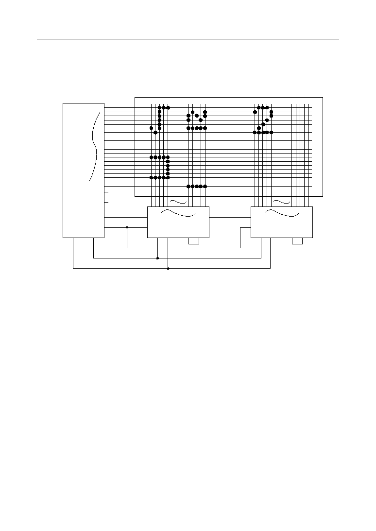
° Semiconductor
MSM6262-xx
44/52
APPLICATION CIRCUITS
LCD
O
1
O
40
DI
1
CP
LOAD DF
DO
20
DI
21
MSM5259
O
1
O
40
DI
1
CP
LOAD DF
DO
20
DI
21
MSM5259
DO
40
DF
LOAD
CP
DO
COM48
COM17
COM16
COM1
MSM6262-xx
1 2-line display mode
5 x 7 dots, 2 lines • 16 characters
(Note: COM17 - COM48 should be left open)
° Semiconductor
MSM6262-xx
45/52
LCD
O
1
O
40
DI
1
CP
LOAD DF
DO
20
DI
21
MSM5259
O
1
O
40
DI
1
CP
LOAD DF
DO
20
DI
21
MSM5259
DO
40
DF
LOAD
CP
DO
COM48
COM25
COM24
COM1
MSM6262-xx
2 2-line display mode
5 x 11 dots, 2 lines • 16 characters
(Note: COM25 - COM48 should be left open)
underline
cursor
° Semiconductor
MSM6262-xx
46/52
LCD
O
1
O
40
DI
1
CP
LOAD DF
DO
20
DI
21
MSM5839C
O
1
O
40
DI
1
CP
LOAD DF
DO
20
DI
21
MSM5839C
DO
40
DF
LOAD
CP
DO
COM48
COM33
COM32
COM1
MSM6262-xx
3 4-line display mode
5 x 7 dots, 4 lines • 16 characters
(Note: COM33 - COM48 should be left open)
° Semiconductor
MSM6262-xx
47/52
LCD
O
1
O
40
DI
1
CP
LOAD DF
DO
20
DI
21
MSM5839C
O
1
O
40
DI
1
CP
LOAD DF
DO
20
DI
21
MSM5839C
DO
40
DF
LOAD
CP
DO
COM48
COM1
MSM6262-xx
4 4-line display mode
5 x 11 dots, 4 lines • 16 characters

° Semiconductor
MSM6262-xx
48/52
∑
Example of connection with MSM5839C and bias circuit
DI
1
O
1
~ O
40
DO
40
MSM5839C
CP LOAD
DF
V
DD
V
SS
DI
21
DO
20
DI
1
O
1
~ O
40
DO
40
MSM5839C
CP LOAD
DF
V
DD
V
SS
DI
21
DO
20
DI
1
O
1
~ O
40
DO
40
MSM5839C
CP LOAD
DF
V
DD
V
SS
V
3
V
EE
DI
21
DO
20
LCD
MSM6262-xx
COM1
COM48
DO
CP
LOAD
DF
V
DD
V
SS
V
1
V
4
V
5
0 V
5
V
≠5 V
C
C
C
C
C
C
C
R
R
4R
R
R
VR
r
V
2
V
3
V
EE
V
2
V
3
V
EE
V
2
V
3
V
EE
V
2
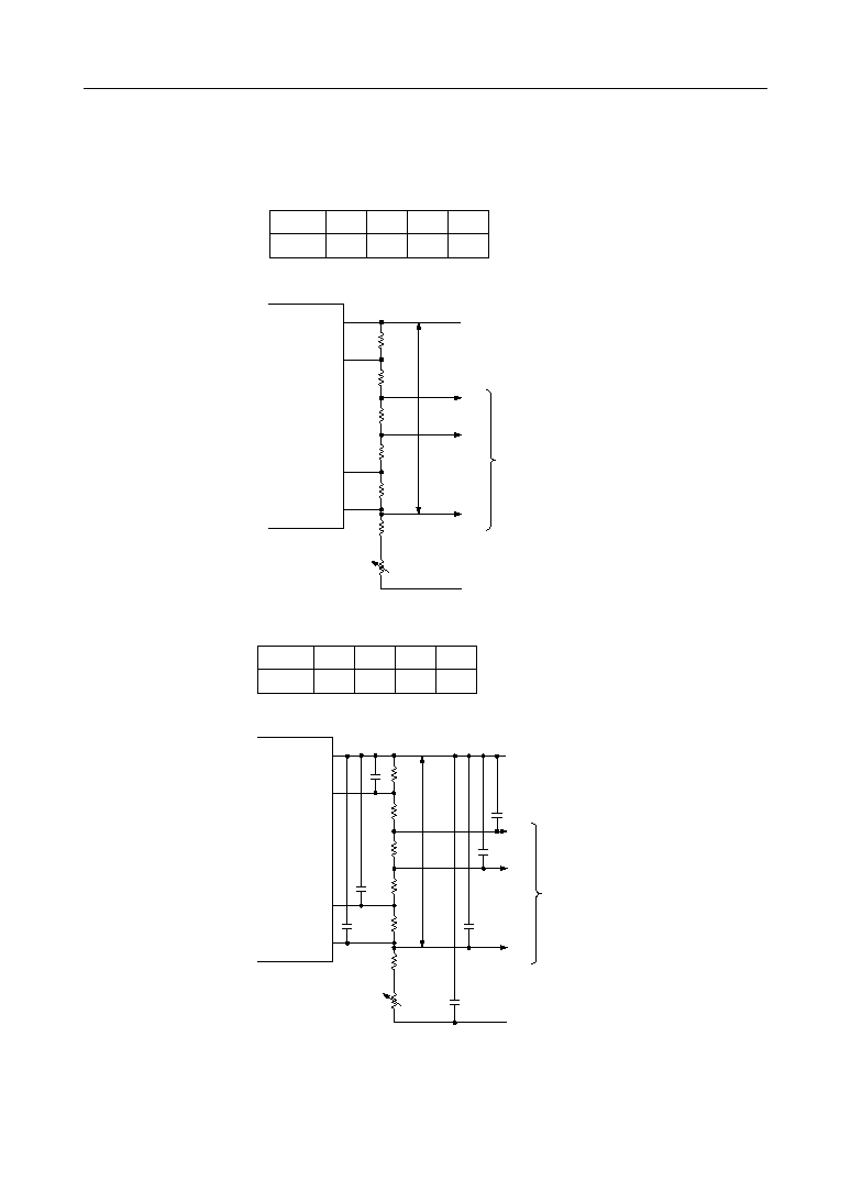
° Semiconductor
MSM6262-xx
49/52
∑
Example of bias circuit
V
DD
V
1
V
4
V
5
MSM6262-xx
R
R
RR
R
R
VR
r
V
LCD
V
2
V
3
V
EE
to segment
driver
1/5 - 1/8 bias example 2.
Bias
RR
1/5
1/6
1/7
1/8
R
2R
3R
4R
V
LCD
: LCD driving voltage
V
DD
V
1
V
4
V
5
MSM6262-xx
R
R
RR
R
R
VR
r
V
LCD
V
2
V
3
V
EE
to segment
driver
C
C
C
C
C
C
C
1/5 - 1/8 bias example 1.
Bias
RR
1/5
1/6
1/7
1/8
R
2R
3R
4R
V
LCD
: LCD driving voltage
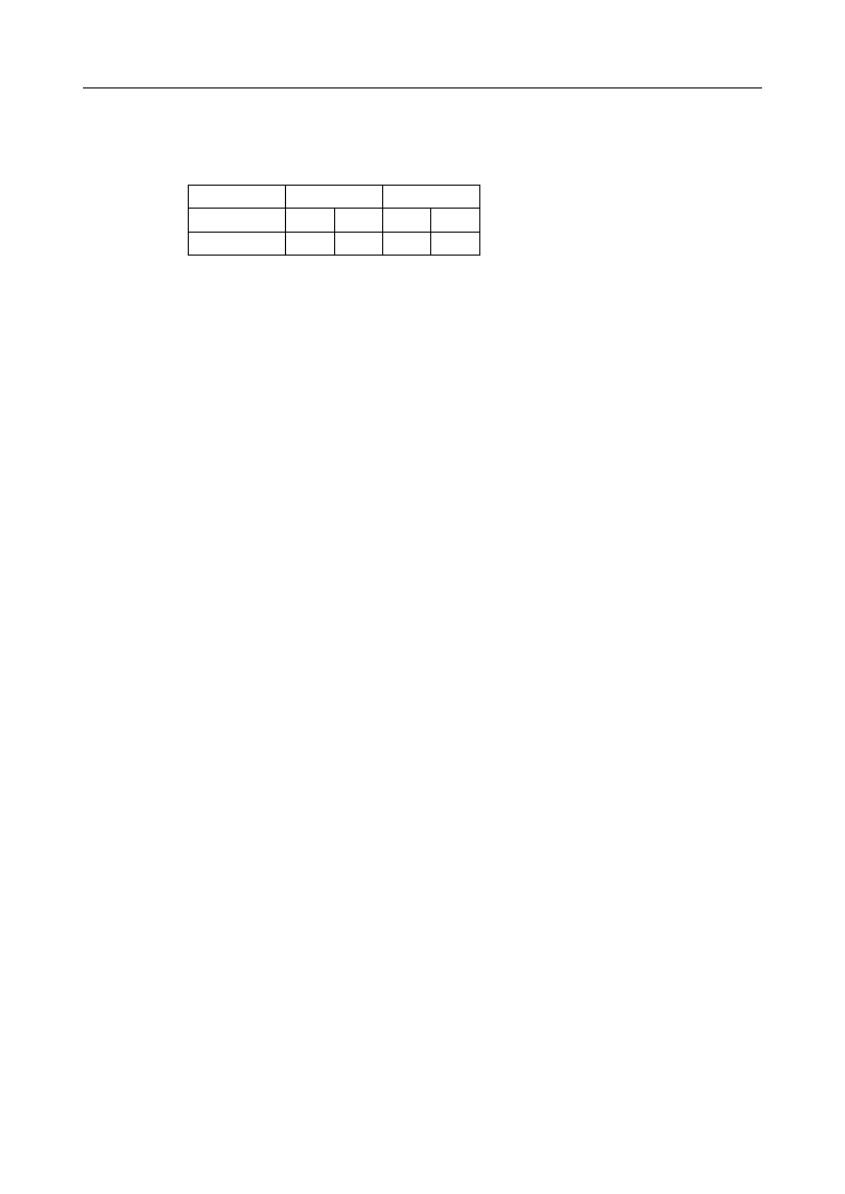
° Semiconductor
MSM6262-xx
50/52
∑
LCD duty and bias
No. of lines
2 lines
4 lines
Duty
Bias
1/16
1/24
1/32
1/48
1/5
1/6
1/7
1/8
Above are examples of relation between LCD duty and bias. Use these values for reference,
for they vary depending on the characteristics of LCD panel.
The value of resistor on bias circuit is determined by the operational margin and power
consumption. To make the power consumption lower, the value of resistor has to be larger,
but it makes the LCD driving output impedance high and causes the distortion on the LCD
driving waveform.
If a large LCD panel is used, the value of the resistor should be much lower because the
LCD capacitance increases.
Connecting a bypass capacitor to the bias resistor in parallel can improve the distortion of
LCD driving waveform. However, connecting a capacitor of too large value may cause a
level shift of the bias voltage.
So, it has to be determined carefully after checking experimentally.
Followings are the reference values.
R = 2 to 10 kW
V
R
= 10 to 50 kW
r = 0.2 to 2 kW
C = 0.0022 to 0.047 mF
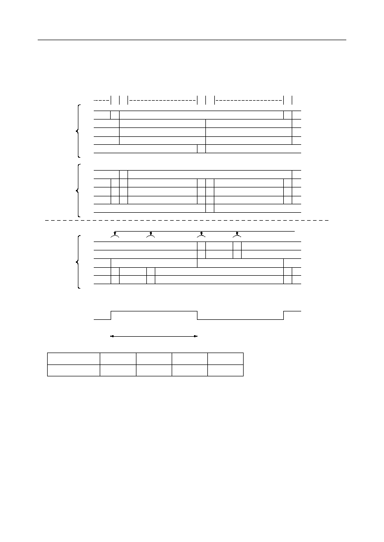
° Semiconductor
MSM6262-xx
51/52
∑
LCD driving waveform (at 1/5 to 1/8 bias)
Selecting a SEGMENT driver IC
V
DD
V
1
V
2
V
3
V
4
V
5
COM1
1 2
1 2
1 2
V
DD
V
1
V
2
V
3
V
4
V
5
COM2
V
DD
V
1
V
2
V
3
V
4
V
5
SEG
Lighting waveform
Duty
1/16
1/24
1/32
1/48
Frame frequency
78.125 Hz
52.08 Hz
78.125 Hz
52.08 Hz
DF
1 frame
Note: f
osc
= 500 kHz
When V
LCD
is within the voltage range of V
DD
and that of V
SS
, MSM5259 is recommendable as
SEGMENT driver. When V
LCD
is beyond the voltage range of V
DD
and that of V
SS
, MSM5839C
or MSM5260 is recommendable as SEGMENT driver.
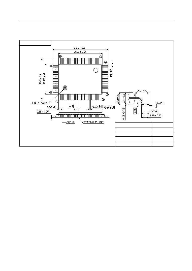
° Semiconductor
MSM6262-xx
52/52
(Unit : mm)
PACKAGE DIMENSIONS
Notes for Mounting the Surface Mount Type Package
The SOP, QFP, TSOP, SOJ, QFJ (PLCC), SHP and BGA are surface mount type packages, which
are very susceptible to heat in reflow mounting and humidity absorbed in storage.
Therefore, before you perform reflow mounting, contact Oki's responsible sales person for the
product name, package name, pin number, package code and desired mounting conditions
(reflow method, temperature and times).
QFP80-P-1420-0.80-BK
Package material
Lead frame material
Pin treatment
Solder plate thickness
Package weight (g)
Epoxy resin
42 alloy
Solder plating
5 mm or more
1.27 TYP.
Mirror finish