
1/9
° Semiconductor
MSM6353/6353L-xx
° Semiconductor
MSM6353/6353L-xx
Built-in 8 or 5 bit Serial Port 4-Bit Microcontroller
GENERAL DESCRIPTION
The MSM6353/6353L is a low-power 4-bit microcontroller manufactured in CMOS process
technology. It is best suited for the control of battery-driven equipment. The built-in 8-bit or
5-bit serial port provides a data communication capability with external apparatus.
FEATURES
∑ Low power consumption
∑ Large capacity memory
∑ ROM
: 4096 words • 15 bits
∑ RAM
: 1024 words • 4 bits
∑ I/O port
Input-output port
: 5 ports • 4 bits (input or output can be specified for each port)
∑ 1.5 V single-power-supply operation (MSM6353)
Can be changed to 3.0 V specification by mask option (MSM6353L).
∑ Built-in watchdog timer
∑ Built-in serial port of 8 bits or 5 bits (asynchronous)
∑ 32.768 kHz built-in crystal oscillator circuit
∑ Package options:
42-pin shrink DIP (SDIP42-P-600-1.78)
(Product name: MSM6353-xxSS, MSM6353L-xxSS)
44-pin plastic QFP (QFP44-P-910-0.80-K) (Product name:MSM6353-xxGS-K, MSM6353L-xxGS-K)
(QFP44-P-910-0.80-2K) (Product name: MSM6353-xxGS-2K, MSM6353L-xxGS-2K)
xx indicates the code number.
E2E0012-27-Y3
This version: Jan. 1998
Previous version: Mar. 1996
2/9
° Semiconductor
MSM6353/6353L-xx
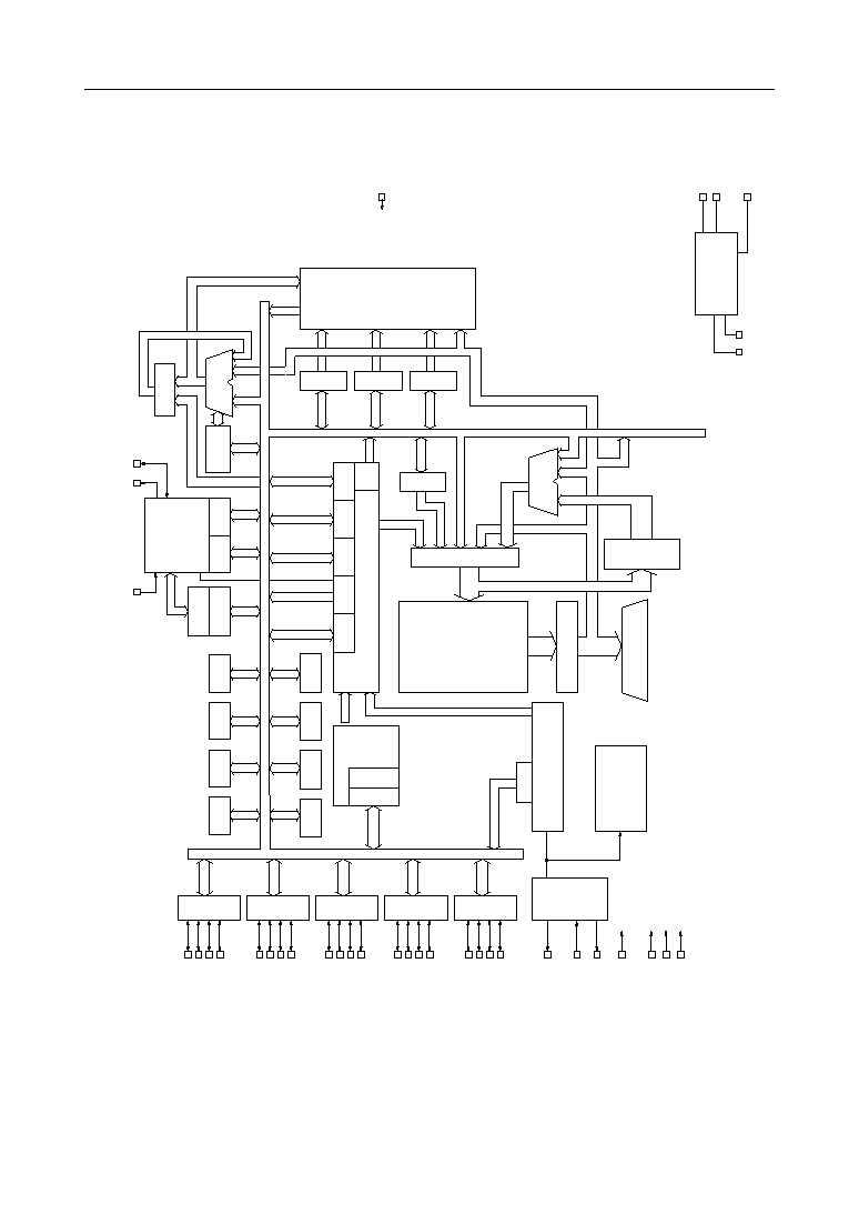
BLOCK DIAGRAM
P0.0 P0.1 P0.2 P0.3
P1.0 P1.1 P1.2 P1.3
P2.0 P2.1 P2.2 P2.3
P3.0 P3.1 P3.2 P3.3
P4.0 P4.1 P4.2 P4.3
XTOUT
XT
XT
RESET
TEST1
TEST2
TEST3
PORT0
PORT1
PORT2
PORT3
PORT4
OSC
SYSTEM CLOCK GENERATOR
P03C
P02C
P01C
P00C
P4
•
C
P3
•
C
P2
•
C
P1
•
C
SBFFl
SBFF u
SIN
SERIAL
I/O
SCNT
SCND
SOUT
SCLK
ALU
ACC
FLAG
D-BUS
EIRT
IRQRT
IEXM0
IEXM1
IEXM2
IRQEX
WDOG 0
WDOG 1
WATCH-
DOG TIMER
P2.0-2.3
TMOUT
TIME BASE COUNTER
INSTRUCTION
DECODER
INSTRUCTION
REGISTER
PROGRAM ROM
4096
•
15 bits
INTERRUPT CONTROL
PROGRAM COUNTER
FRMT
ADDER
STACK
WORK
PAGE
BANK
DATA RAM
1024
•
4 bits
V
DD
V
SS1
V
SS2
V
EE
V
CM
V
CP
VOLTAGE CONVERTER REGURATOR
3/9
° Semiconductor
MSM6353/6353L-xx
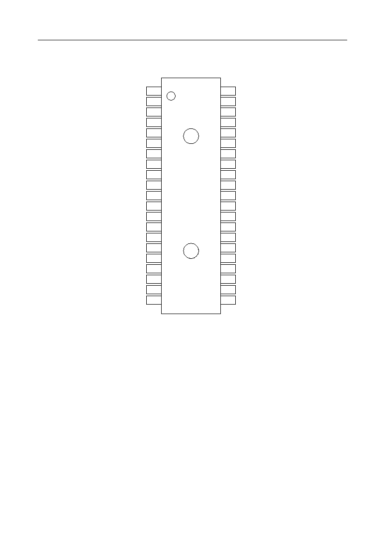
PIN CONFIGURATION (TOP VIEW)
20
1
2
3
4
5
6
7
8
9
10
11
12
13
14
15
16
17
18
19
P2.2
V
DD
V
SS2
V
SS1
V
EE
NC
V
CP
V
CM
NC
SOUT
SIN
SCLK
NC
P0.0
P0.1
P0.2
P0.3
NC
P2.0
P2.1
P3.1
XT
XT
XTOUT
P1.0
P1.1
P1.2
P1.3
NC
TEST3
TEST2
TEST1
RESET
P4.3
P4.2
P4.1
P4.0
NC
P3.3
P3.2
23
42
41
40
39
38
37
36
35
34
33
32
31
30
29
28
27
26
25
24
21
P2.3
P3.0
22
NC : No-connection pin
42-Pin Shrink DIP
4/9
° Semiconductor
MSM6353/6353L-xx
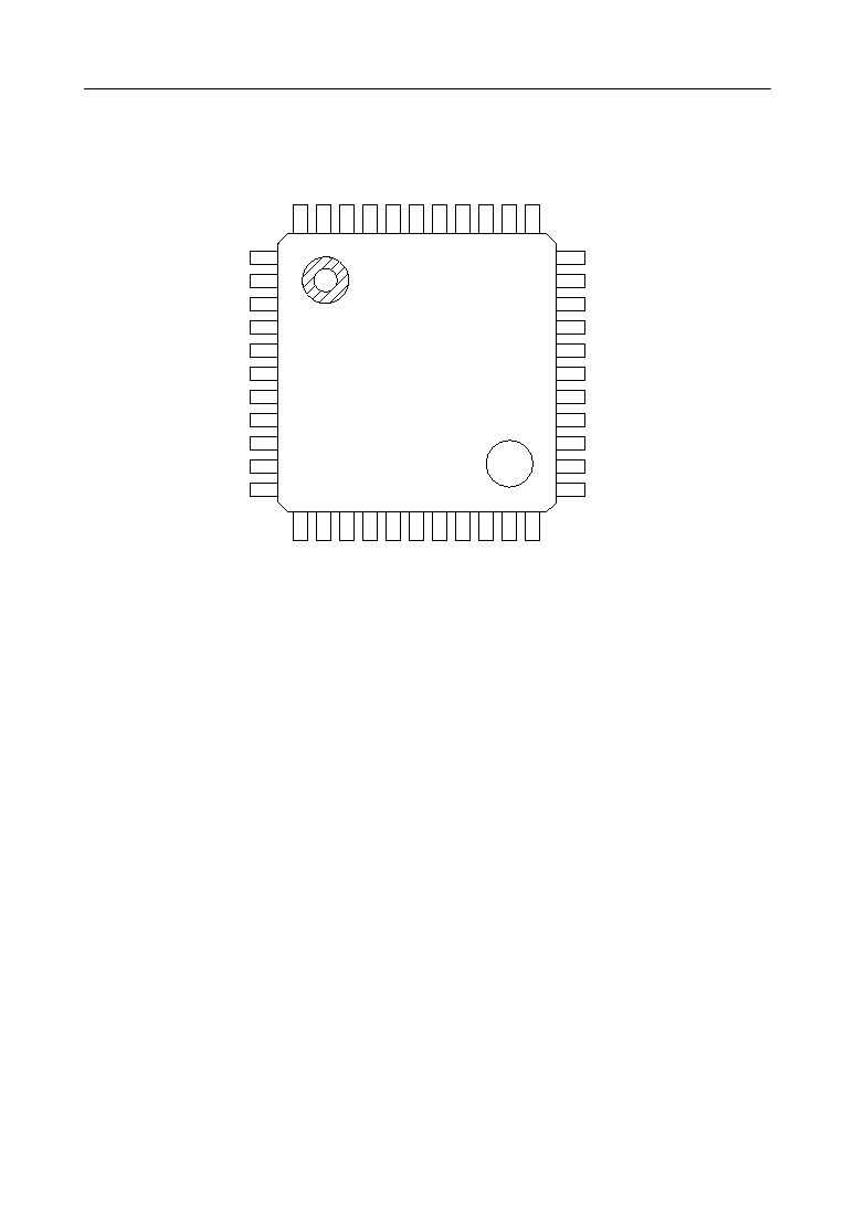
PIN CONFIGURATION (TOP VIEW) (Continued)
33
32
31
30
29
28
27
26
25
24
23
1
2
3
4
5
6
7
8
9
10
11
NC
V
CP
V
CM
NC
SOUT
SIN
SCLK
P0.0
P0.1
P0.2
P0.3
P1.1
P1.2
P1.3
TEST3
TEST2
TEST1
RESET
P4.3
P4.2
P4.1
P4.0
44
43
42
41
40
39
38
37
36
35
34
NC
NC
V
EE
V
SS1
V
SS2
V
DD
V
DD
XT
XT
XTOUT
P1.0
12
13
14
15
16
17
18
19
20
21
22
NC
P2.0
P2.1
P2.2
P2.3
P2.3
P3.0
P3.1
P3.2
P3.3
NC
NC : No-connection pin
44-Pin Plastic QFP
5/9
° Semiconductor
MSM6353/6353L-xx
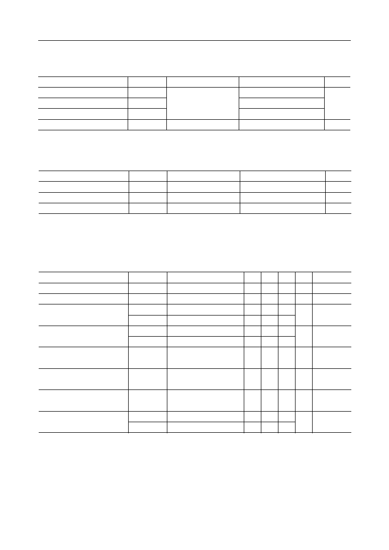
ABSOLUTE MAXIMUM RATINGS (MSM6353, 1.5 V)
Parameter
Symbol
Condition
Unit
Power Supply Voltage
V
Ta=25∞C
Rating
≠6.0 to +0.3
Input Voltage
--
V
SS1
Storage Temperature
Output Voltage
V
DD
=0 V (V
SS1
=V
SS2
=battery voltage)
V
IN
V
OUT
T
STG
∞C
V
SS
≠0.3 to V
SS
+0.3
V
SS
≠0.3 to V
SS
+0.3
≠55 to +125
RECOMMENDED OPERATING CONDITIONS (MSM6353, 1.5 V)
Parameter
Symbol
Condition
Unit
Operating Voltage
V
BUF=Fixed to "0"
Range
≠1.25 to ≠1.75
Operating Temperature
V
op
Operating Frequency
V
DD
=0 V (V
SS1
=V
SS2
=battery voltage)
T
op
f
OSC
≠20 to +70
32.768
--
--
∞C
kHz
ELECTRICAL CHARACTERISTICS (MSM6353, 1.5 V)
DC Characteristics
Parameter
Symbol
Condition
Unit
Current Consumption
mA
*1 *2
Oscillation Start Voltage
Output Current 1
--
Applied Pin
(V
DD
=0 V, V
SS1
=V
SS2
=≠1.5 V (battery voltage), f
OSC
=32,768 Hz, C
X
=35 pF, Ta=25∞C)
Min. Typ. Max.
Output Current 2
Input Current 1
Input Leakage Current
Input Current 3
Input Voltage
I
DD
| I
IL2
|
≠I
IL3
≠I
IH1
≠V
IH
≠V
IL
V
I
=0 V,
input state,
with pull-down resistor
V
I
=0V, ≠1.5 V, input state,
without pull-down resistor
V
I
=0 V,
with pull-down resistor
--
mA
V
--
--
PORT0 to PORT4
PORT0 to PORT4
SCLK, SIN, SOUT
RESET
All input pins
PORT0 to PORT4*3
SOUT, SCLK, XTOUT
BD
mA
mA
mA
mA
V
≠V
OSC
≠I
OH1
I
OL1
≠I
OH2
I
OL2
Within 2 sec.
V
O
=≠0.5 V
V
O
=≠1.0 V
V
O
=≠0.5 V
V
O
=≠1.0 V
--
--
150
150
7
20
75
--
--
--
1.2
3.0
--
--
--
--
--
150
--
4
--
--
--
1.4
--
--
--
--
300
1
--
0.3
--
*1 This value depends on program.
*2 Backup flag (BUF)=fixed to "0".
*3 PORT0=P0.0-P0.3, PORT1=P1.0-P1.3, PORT2=P2.0-P2.3, PORT3=P3.0-P3.3, PORT4=P4.0-
P4.3.
6/9
° Semiconductor
MSM6353/6353L-xx
ABSOLUTE MAXIMUM RATINGS (MSM6353L, 3.0 V)
Parameter
Symbol
Condition
Unit
Power Supply Voltage
V
Ta=25∞C
Rating
≠6.0 to +0.3
Input Voltage
--
V
SS1
Storage Temperature
Output Voltage
V
DD
=0 V (V
SS1
=V
SS2
=battery voltage)
V
IN
V
OUT
T
STG
∞C
V
SS
≠0.3 to V
SS
+0.3
V
SS
≠0.3 to V
SS
+0.3
≠55 to +125
RECOMMENDED OPERATING CONDITIONS (MSM6353L, 3.0 V)
Parameter
Symbol
Condition
Unit
Operating Voltage
V
BUF=Fixed to "1"
Range
≠2.2 to ≠3.5
Operating Temperature
V
op
Operating Frequency
V
DD
=0 V (V
SS1
=V
SS2
=battery voltage)
T
op
f
OSC
≠20 to +70
32.768
--
--
∞C
kHz
ELECTRICAL CHARACTERISTICS (MSM6353L, 3.0 V)
DC Characteristics
Parameter
Symbol
Condition
Unit
Current Consumption
mA
*1 *2
Oscillation Start Voltage
Output Current 1
--
Applied Pin
(V
DD
=0 V, V
SS1
=V
SS2
=≠3.0 V (battery voltage), f
OSC
=32,768 Hz, C
X
=35 pF, Ta=25∞C)
Min. Typ. Max.
Output Current 2
Input Current 1
Input Leakage Current
Input Current 3
Input Voltage
I
DD
| I
IL2
|
≠I
IL3
≠I
IH1
≠V
IH
≠V
IL
V
I
=0 V,
input state,
with pull-down resistor
V
I
=0 V, ≠3 V, input state,
without pull-down resistor
V
I
=0 V,
with pull-down resistor
--
mA
V
--
--
PORT0 to PORT4
PORT0 to PORT4
SCLK, SIN, SOUT
RESET
All input pins
PORT0 to PORT4*3
SOUT, SCLK, XTOUT
BD
mA
mA
mA
mA
V
≠V
OSC
≠I
OH1
I
OL1
≠I
OH2
I
OL2
Within 2 sec.
V
O
=≠0.5 V
V
O
=≠2.5 V
V
O
=≠0.5 V
V
O
=≠2.5 V
--
--
500
500
7
20
150
--
--
--
2.5
3.0
--
--
--
--
--
300
--
25
--
--
--
2.4
--
--
--
--
600
1
--
0.5
--
*1 This value depends on program.
*2 Backup flag (BUF)=fixed to "1".
*3 PORT0=P0.0-P0.3, PORT1=P1.0-P1.3, PORT2=P2.0-P2.3, PORT3=P3.0-P3.3, PORT4=P4.0-
P4.3.

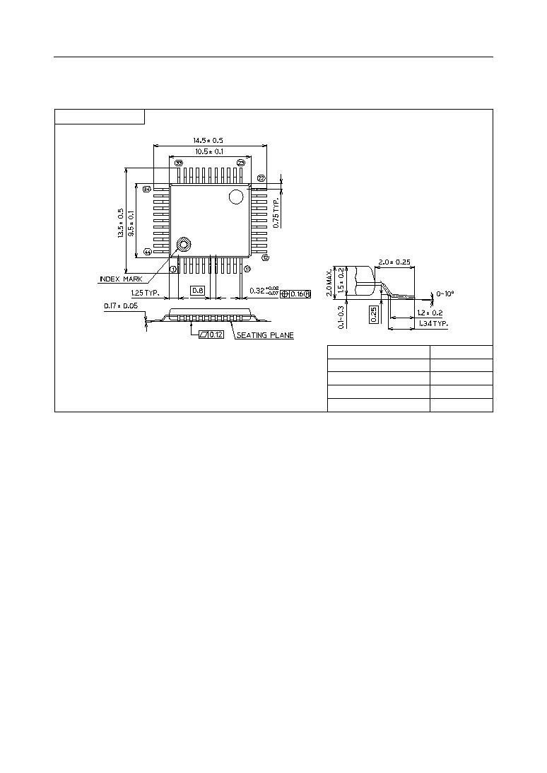
7/9
° Semiconductor
MSM6353/6353L-xx
(Unit : mm)
PACKAGE DIMENSIONS
Notes for Mounting the Surface Mount Type Package
The SOP, QFP, TSOP, SOJ, QFJ (PLCC), SHP and BGA are surface mount type packages, which
are very susceptible to heat in reflow mounting and humidity absorbed in storage.
Therefore, before you perform reflow mounting, contact Oki's responsible sales person for the
product name, package name, pin number, package code and desired mounting conditions
(reflow method, temperature and times).
SDIP42-P-600-1.78
Package material
Lead frame material
Pin treatment
Solder plate thickness
Package weight (g)
Epoxy resin
42 alloy
Solder plating
5
mm or more
4.52 TYP.
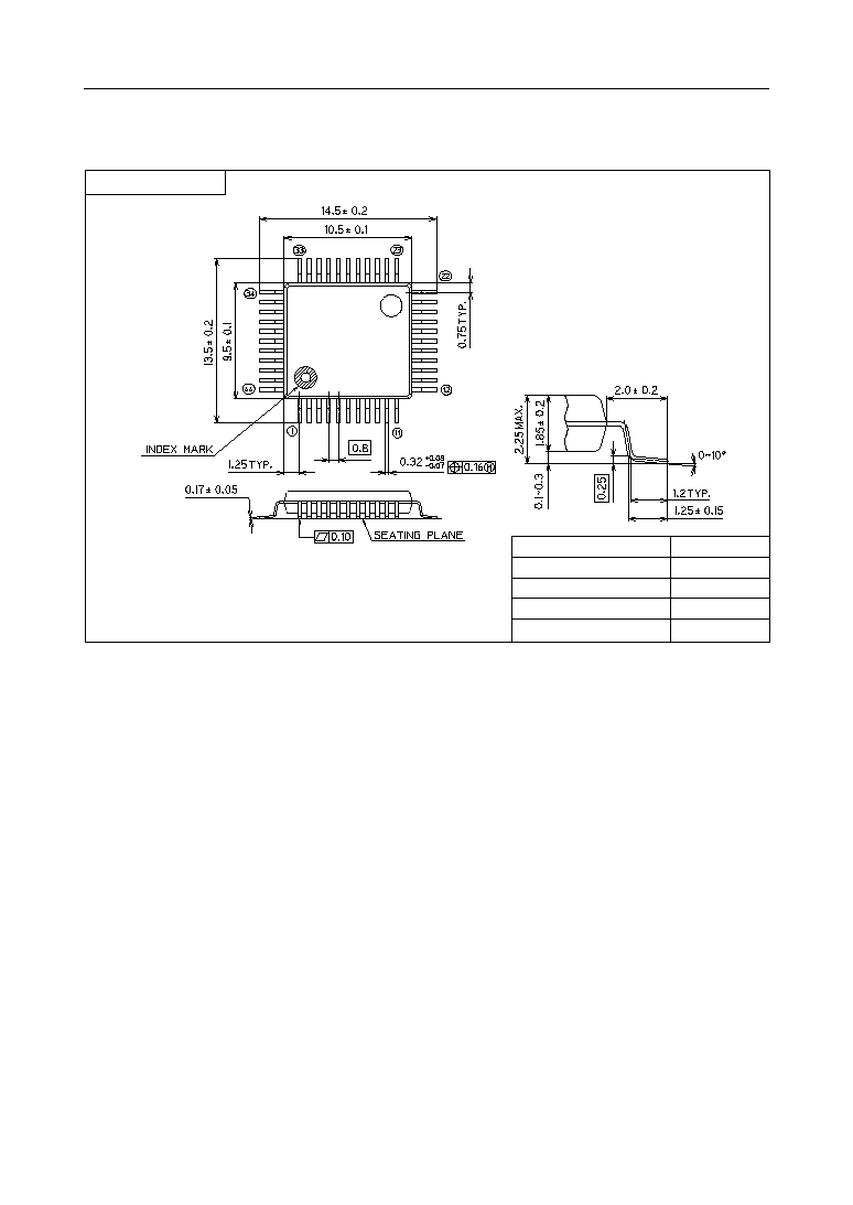
8/9
° Semiconductor
MSM6353/6353L-xx
(Unit : mm)
Notes for Mounting the Surface Mount Type Package
The SOP, QFP, TSOP, SOJ, QFJ (PLCC), SHP and BGA are surface mount type packages, which
are very susceptible to heat in reflow mounting and humidity absorbed in storage.
Therefore, before you perform reflow mounting, contact Oki's responsible sales person for the
product name, package name, pin number, package code and desired mounting conditions
(reflow method, temperature and times).
QFP44-P-910-0.80-K
Package material
Lead frame material
Pin treatment
Solder plate thickness
Package weight (g)
Epoxy resin
42 alloy
Solder plating
5
mm or more
0.35 TYP.
Mirror finish
9/9
° Semiconductor
MSM6353/6353L-xx
(Unit : mm)
Notes for Mounting the Surface Mount Type Package
The SOP, QFP, TSOP, SOJ, QFJ (PLCC), SHP and BGA are surface mount type packages, which
are very susceptible to heat in reflow mounting and humidity absorbed in storage.
Therefore, before you perform reflow mounting, contact Oki's responsible sales person for the
product name, package name, pin number, package code and desired mounting conditions
(reflow method, temperature and times).
Package material
Lead frame material
Pin treatment
Solder plate thickness
Package weight (g)
Epoxy resin
42 alloy
Solder plating
5
mm or more
0.41 TYP.
QFP44-P-910-0.80-2K
Mirror finish