 | –≠–ª–µ–∫—Ç—Ä–æ–Ω–Ω—ã–π –∫–æ–º–ø–æ–Ω–µ–Ω—Ç: MSM64P164 | –°–∫–∞—á–∞—Ç—å:  PDF PDF  ZIP ZIP |

1/37
° Semiconductor
MSM64P164
° Semiconductor
MSM64P164
4-Bit Microcontroller with Built-in RC Oscillation Type A/D Converter and LCD Driver
GENERAL DESCRIPTION
The MSM64P164 is a one-time-programmable ROM-version product, which has one-time
PROM (OTP) as internal program memory. On the other hand, the MSM64164C is a mask ROM-
version product, which has mask ROM as internal program memory.
Unlike the mask ROM-version MSM64164C, which has a P-well CMOS structure, the MSM64P164
has been fabricated with the N-well CMOS-structured EEPROM process technology. Therefore,
the MSM64P164 differs from the MSM64164C in the polarity of the power supply for LCD bias
generation and 5 V interface, and in the external circuit structure.
Unlike the mask ROM-version product, the MSM64P164 cannot be supplied in the form of a chip.
The MSM64P164 is an OTP-version product used to evaluate an application program.
The MSM64P164 has two operation modes, microcontroller operation mode and PROM mode.
The microcontroller operation mode is used to operate the MSM64P164 like a mask ROM-version
product and the PROM mode is used to program or read the PROM.
FEATURES
∑ Operating range
Operating frequencies
:
32.768 kHz, 400 kHz
Operating voltage
:
1.5 V/3.0 V selectable by mask option
Low supply current
Operating temperature
:
0 to +65
∞
C
∑ Memory space
Internal program memory
:
4064 bytes
Internal data memory
:
256 nibbles
∑ RC oscillation type A/D converter
:
2 channels
Time dividing 2-channel method
Counter A
:
1/(10
4
• 8) • 1
Counter B
:
1/2
14
• 1
∑ Serial port
:
Synchronous 8-bit transfer
External clock/internal clock selectable
MSB first/LSB first selectable
∑ LCD driver
:
34 outputs; duty ratio switchable by software
(1) At 1/4 duty and 1/3 bias
:
120 segments (max)
(2) At 1/3 duty and 1/3 bias
:
93 segments (max)
(3) At 1/2 duty and 1/2 bias
:
64 segments (max)
∑ Buzzer driver
:
1 output (4 output modes selectable)
∑ Capture circuit
:
2 channels (256 Hz, 128 Hz, 64 Hz, 32 Hz)
∑ Watchdog timer
∑ I/O port
Input-output port
:
3 ports • 4 bits
Input port
:
1 port • 4 bits
Output port
:
1 port • 4 bits
E2E0045-38-96
This version: Sep. 1998
Previous version: Sep. 1995
Preliminary

2/37
° Semiconductor
MSM64P164
∑ Interrupt sources
External interrupt
:
2 sources
Internal interrupt
:
8 sources
∑ Package:
80-pin plastic QFP (QFP80-P-1420-0.80-BK) : (Product name : MSM64P164-•••GS-BK)
••• indicates a code number.
3/37
° Semiconductor
MSM64P164
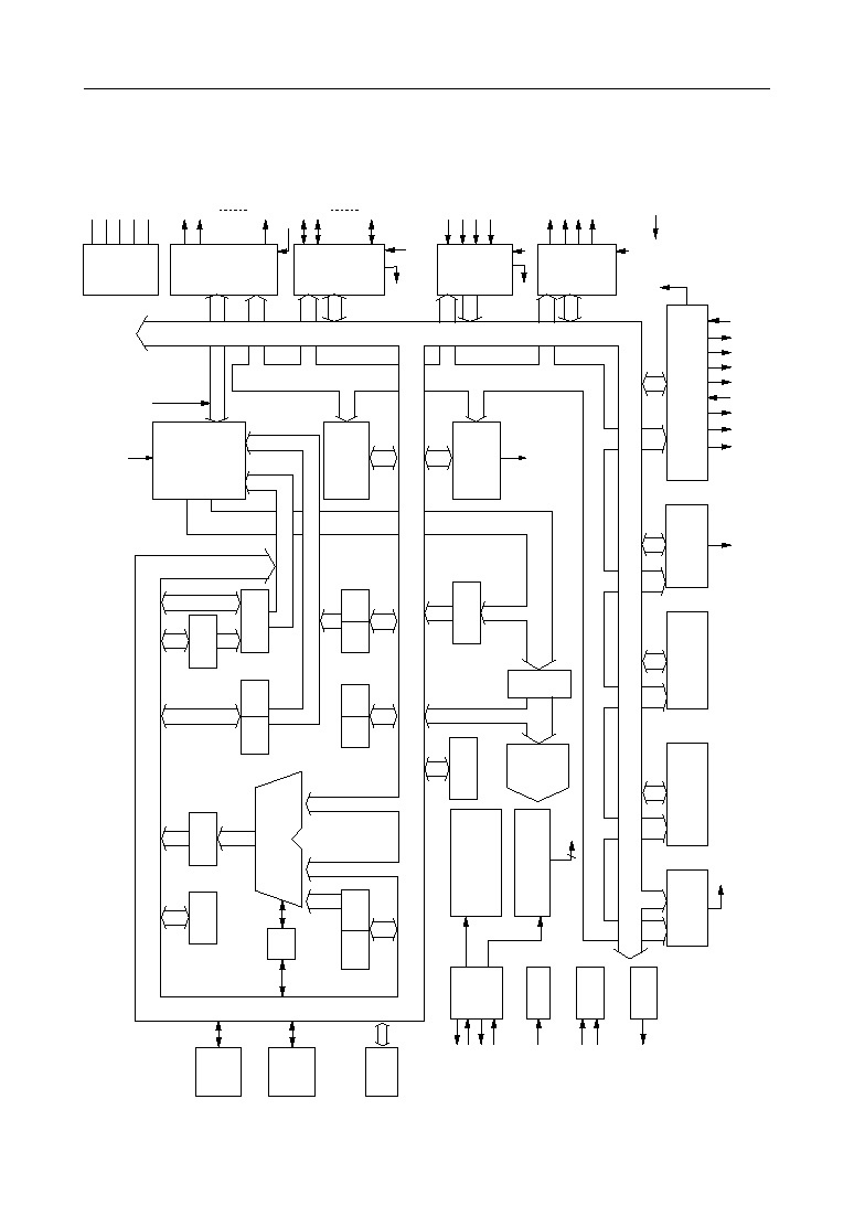
BLOCK DIAGRAM
BSR
HALT
MIEF
TR2
TR0
TR1
C
ALU
B
A
PCM PCL
(4)
(4)
(4)
PCH
H
L
X
Y
A11 to A8
A7 to A0
DB7 to DB0
(8)
PROM
(4064
bytes)
BIAS
RAM
(256
nibbles)
IR
SIOP
INT
(8)
ROMR
SP
TIMING
CONTROLLER
I∑R
DECO-
DER
DB7 to DB0
V
DD1
V
DD2
V
DD3
C1
C2
LCD
L0
L1
P2.0
P4.3
V
DD
P0
P0.0
P0.1
P0.2
INT
P1.0
P1.1
BD
INTC
WDT
BD
INT
TBC
INT
2CLK
RSTG
TST
VR
OSC2
OSC1
XT
XT
RESET
TST1
TST2
V
SSL
P2.1
V
DD
INT
P1.2
5
P1
P1.3
V
SS
L33
V
DD
INT
P2
P3
P4
P0.3
V
DD
CAPR
ADC
IN0
CS0
RS0
CRT0
RT0
IN1
CS1
RS1
RT1
PORT ADDRESS
PORT ADDRESS
Program
data/address
V
PP
4/37
° Semiconductor
MSM64P164
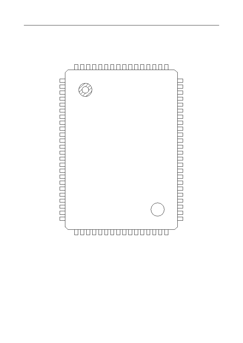
PIN CONFIGURATION (TOP VIEW)
80-Pin Plastic QFP
Note: Because pin 32 and pin 67 are internally connected with each other, V
DD
can be supplied
from either pin 32 or pin 67.
RT1
41
V
DD1
42
V
DD
43
V
DD2
44
V
DD3
45
C1
46
C2
47
L17/A7
48
L18/A8
49
L19/A9
50
L20/A10
51
L21/A11
52
L22
53
L23
54
L24
55
L25
56
L26/P5.0
57
L27/P5.1
58
L28/P5.2
59
L29/P5.3
60
L30/P6.0
61
L31/P6.1
62
L32/P6.2
63
L33/P6.3
64
RS1
40
CS1
39
IN1
38
IN0
37
CS0
36
RS0
35
CRT0
34
RT0
33
V
SS
32
V
PP
31
BD
30
P4.3
29
P4.2
28
P4.1
27
P4.0
26
P3.3
25
24
23
22
21
20
19
18
17
16
15
14
13
12
11
10
9
8
7
6
5
4
3
2
1
P3.2
P3.1
P3.0
P2.3
P2.2
P2.1
P2.0
L16/A6
L15/A5
L14/A4
L13/A3
L12/A2
L11/A1
L10/A0
L9/OE
L8/CE
L7/D7
L6/D6
L5/D5
L4/D4
L3/D3
L2/D2
L1/D1
L0/D0
65
66
67
68
69
70
71
72
73
74
75
76
77
78
79
80
OSC2
OSC1
V
DD
XT
XT
RESET
TST1
TST2
P1.0
P1.1
P1.2
P1.3
P0.0
P0.1
P0.2
P0.3
5/37
° Semiconductor
MSM64P164
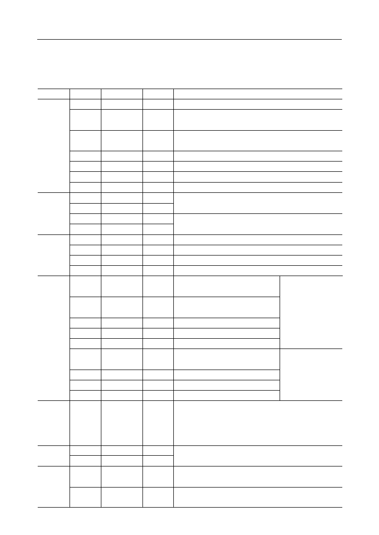
PIN DESCRIPTIONS
Basic Functions
Function
Symbol
Type
Description
0 V power supply
Power
Supply
V
SS
Bias output for driving LCD (+1.5 V), or positive power supply
at 1.5 V spec.
V
DD1
Bias output for driving LCD (+3.0 V), or positive power supply
at 3.0 V spec.
V
DD2
Bias output for driving LCD (+4.5 V).
V
DD3
Positive power supply for I/O port interface
V
DD
Positive power supply for writing to PROM (+12.5 V)
V
PP
Pins for connecting a capacitor for generating LCD driving bias.
C1, C2
32.768 kHz crystal connection pins
XT
XT
External 400 kHz oscillation resistor (R
OS
) connection pins
OSC1
OSC2
Output port (P1.0 : high current output)
P1.0 to P1.3
Input-output ports
P2.0 to P4.3
Output pin for the buzzer driver
BD
LCD driver pins
L0 to L25
Oscillation
I
O
I
O
Ports
O
I/O
O
O
LCD driver pins, or output ports by mask option
L26/P5.0 to
L33/P6.3
O
Input pin for RC oscillator circuit
IN0
I
Input pin for RC oscillator circuit
IN1
I
System reset input pin.
Setting this pin to "L" level puts this device into a reset state.
Them, setting this pin to "H" level starts executing an instruction
from address 000H.
This pin is internally pulled up to V
DD
.
RESET
I
Input pins for testing.
TST1
I
TST2
I
Test
Reset
Input port
P0.0 to P0.3
I
Resistance temperature sensor
connection pin
RT0
O
Resistance/capacitance temperature
sensor connection pin
CRT0
O
Reference resistor connection pin
RS0
O
Reference capacitor connection pin
CS0
O
Resistance temperature sensor
connection pin
RT1
O
Reference resistor connection pin
RS1
O
Reference capacitor connection pin
CS1
O
A/D
Converter
RC oscillation pins
for A/D converter
(channel 0)
(CROSC0)
RC oscillation pins
for A/D converter
(channel 1)
(CROSC1)
--
--
--
--
--
--
--
LCD
Drivers
Pin
69
68
66
65
73 to 76
18 to 29
30
1 to 17,
48 to 56
57 to 64
37
38
70
71
72
77 to 80
33
34
35
36
41
40
39
32
42
44
45
43
31
46,47
6/37
° Semiconductor
MSM64P164
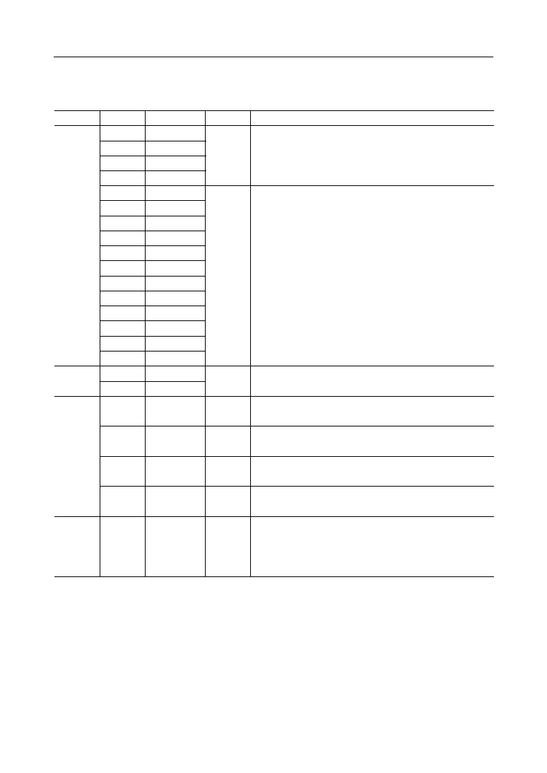
Secondary Functions
Function
Symbol
Description
External
Interrupt
P0.0
Secondary functions of P0.0 to P0.3:
Level-triggered external interrupt input pins.
The change of input signal level causes an interrupt to occur.
P0.1
P0.2
P0.3
Type
P2.0
P2.1
P2.2
P2.3
P3.0
P3.1
P3.2
P3.3
P4.0
P4.1
P4.2
P4.3
P0.0
P0.1
P3.3
P4.0
P4.1
P4.2
P4.3
I
I
I
I
O
O
I/O
O
Secondary functions of P2.0 to P2.3, P3.0 to P3.3, and P4.0 to P4.3:
Level-triggered external interrupt input pins.
The change of input signal level causes an interrupt to occur.
Secondary functions of P0.0 and P0.1:
Capture circuit trigger input pins.
Secondary functions of P3.3:
This pin is assigned the data input of a serial port (SIN).
Secondary functions of P4.0:
This pin is assigned the data output of a serial port (SOUT).
Secondary functions of P4.1:
This pin is assigned the ready output of a serial port (SPR).
Secondary functions of P4.2:
This pin is assigned the clock I/O of a serial port (SCLK).
Secondary functions of P4.3:
This pin is a monitor output (MON) of an RC oscillation clock
(OSCCLK) for an A/D converter and a 400 kHz RC oscillation
clock for a system clock.
Capture
Trigger
Serial Port
RC Oscillation
Monitor
Pin
77
78
79
80
18
19
20
21
22
23
24
25
26
27
28
29
77
78
25
26
27
28
29
7/37
° Semiconductor
MSM64P164
PROM-Related Pins
Function
Pin
Description
Program-
ming
32, 67
O
0 V power supply.
Type
8
9
I/O
PROM chip enable pin.
10
I/O
PROM output enable signal.
11
I
Program address input pins.
12
13
14
15
16
17
48
49
50
51
52
53
I
Apply a "H" level to this pin.
42
--
Positive power supply pin (+5 V supplied).
44
--
Positive power supply pin (+5 V supplied).
31
--
PROM write power supply (+12.5 V supplied).
70
PROM write setting pins:
PROM mode is set by a "L" level input.
71
I
72
1
I/O
Pins for writing and reading program data.
2
3
4
5
6
7
Symbol
V
SS
L7/D7
L8/CE
L9/OE
L10/A0
L11/A1
L12/A2
L13/A3
L14/A4
L15/A5
L16/A6
L17/A7
L18/A8
L19/A9
L20/A10
L21/A11
L22
V
DD1
*
V
DD2
*
V
PP
RESET
TST1
TST2
L0/D0
L1/D1
L2/D2
L3/D3
L4/D4
L5/D5
L6/D6
*
When in PROM mode, supply a 5 V power to both V
DD1
and V
DD2
.
8/37
° Semiconductor
MSM64P164
ABSOLUTE MAXIMUM RATINGS (1.5 V Spec.)
RECOMMENDED OPERATING CONDITIONS (1.5 V Spec.)
Parameter
Power Supply Voltage 1
Symbol
Condition
Rating
Unit
V
DD1
Ta = 25∞C
≠0.3 to +2.0
V
Power Supply Voltage 2
V
DD2
Ta = 25∞C
≠0.3 to +4.0
V
Power Supply Voltage 3
V
DD3
Ta = 25∞C
≠0.3 to +5.5
V
Power Supply Voltage 4
V
DD
Ta = 25∞C
≠0.3 to +5.5
V
Input Voltage 1
V
IN1
V
DD1
input, Ta = 25∞C
≠0.3 to V
DD1
+ 0.3
V
Input Voltage 2
V
IN2
V
DD
input, Ta = 25∞C
≠0.3 to V
DD
+ 0.3
V
Output Voltage 1
V
OUT1
V
DD1
output, Ta = 25∞C
≠0.3 to V
DD1
+ 0.3
V
Output Voltage 2
V
OUT2
V
DD2
output Ta = 25∞C
≠0.3 to V
DD2
+ 0.3
V
Output Voltage 3
V
OUT3
V
DD3
output, Ta = 25∞C
≠0.3 to V
DD3
+ 0.3
V
Output Voltage 4
V
OUT4
V
DD
output, Ta = 25∞C
≠0.3 to V
DD
+ 0.3
V
Storage Temperature
T
STG
--
≠55 to +150
∞C
(V
SS
= 0 V)
(V
SS
= 0 V)
Operating Temperature
Operating Voltage
T
op
--
0 to +65
∞C
V
DD1
--
1.4 to 1.7
V
V
DD
--
V
DD1
to 5.25
V
External 400 kHz RC Oscillator
Resistance
R
OS
--
250 to 500
kW
Crystal Oscillation Frequency
f
XT
--
30 to 35
kHz
Parameter
Symbol
Condition
Range
Unit
9/37
° Semiconductor
MSM64P164
ELECTRICAL CHARACTERISTICS (1.5 V Spec.)
DC Characteristics
Parameter
+100%
≠50%
Symbol
Condition
Min.
Typ.
Max.
Unit
Measuring
Circuit
V
DD2
Voltage
V
DD2
C
a
, C
b
, C
12
= 0.1 mF
2.8
3.0
3.2
V
V
DD3
Voltage
V
DD3
C
a
, C
b
, C
12
= 0.1 mF
4.3
4.5
4.7
V
Crystal Oscillation
Start Voltage
V
STA
Oscillation start time:
within 5 seconds
1.47
--
--
V
Crystal Oscillation
Hold Voltage
V
HOLD
--
1.40
--
--
V
Crystal Oscillation
Stop Detection Time
T
STOP
--
0.1
--
1000
ms
Internal Crystal
Oscillator Capacitance
C
G
--
10
15
20
pF
External Crystal
Oscillator Capacitance
C
GEX
When external C
G
used
10
--
30
pF
Internal Crystal
Oscillator Capacitance
C
D
--
10
15
20
pF
Internal 400k RC
Oscillator Capacitance
C
OS
--
8
12
16
pF
400k RC Oscillation
Frequency
f
OSC
External resistor R
OS
= 300 kW
V
DD1
= 1.40 to 1.7 V
80
220
350
kHz
POR Generation
Voltage
V
POR1
When V
DD1
is between V
POR1
and 1.5 V
0
--
0.4
V
POR Non-generation
Voltage
V
POR2
No POR when V
DD1
is between
V
POR2
and 1.5 V
1.4
--
1.5
V
+100%
≠50%
1
(V
SS
= 0 V, V
DD1
= V
DD
= 1.5 V, Ta = 0 to +65∞C unless otherwise specified)
Notes: 1. "POR" denotes Power On Reset.
2. "T
STOP
" indicates that if the crystal oscillator stops over the value of T
STOP
, the
system reset occurs.
10/37
° Semiconductor
MSM64P164
DC Characteristics (continued)
Parameter
Symbol
Condition
Min.
Typ.
Max.
Unit
Measuring
Circuit
Supply Current 1
I
DD1
--
2.0
5.0
m
A
Supply Current 2
I
DD2
Supply Current 3
I
DD3
CPU in operating state
(400k RC oscillation in operation)
R
OS
= 300 kW
--
90
180
m
A
Supply Current 4
I
DD4
Serial transfer,
f
SCK
= 300 kHz,
CPU in operating state
(400k RC oscillation halt)
--
60
100
m
A
Supply Current 5
I
DD5
CPU in halt state
(400k RC oscillation
halt), RC oscillator for
A/D converter is in
operating state
--
150
230
m
A
1
(V
SS
= 0 V, V
DD1
= V
DD
= 1.5 V, Ta = 0 to +65∞C unless otherwise specified)
CPU in operating state
(400k RC oscillation halt)
CPU in halt state
(400k RC oscillation halt)
RT0 = 10 kW
RT0 = 2 kW
--
50
80
m
A
--
600
900
m
A
11/37
° Semiconductor
MSM64P164
DC Characteristics (continued)
Parameter
(Pin Name)
Symbol
Condition
Unit
Measuring
Circuit
Output Current 1
(P1.0)
I
OH1
V
OH1
= V
DD
≠ 0.5 V
Min.
Typ.
Max.
≠2.1
≠0.7
≠0.2
mA
I
OL1
V
OL1
= 0.5 V
1.0
3.0
9.0
mA
Output Current 2
(P1.1 to P1.3)
(P2.0 to P2.3)
(P3.0 to P3.3)
(P4.0 to P4.3)
I
OH2
≠2.1
≠0.7
≠0.2
mA
I
OL2
V
OL2
= 0.5 V
0.2
0.7
2.1
mA
2
Output Current 3
(BD)
I
OH3
V
OH3
= V
DD1
≠ 0.7 V
≠1.8
≠0.6
≠0.2
mA
I
OL3
V
OL3
= 0.7 V
0.2
0.6
1.8
mA
Output Current 4
(RT0, RT1, RS0, RS1,
CRT0, CS0, CS1)
I
OH4
V
OH4
= V
DD1
≠ 0.1 V
≠1.1
≠0.6
≠0.3
mA
I
OL4
V
OL4
= 0.1 V
0.3
0.6
1.1
mA
Output Current 5
(When L26 to L33 are
configured as output
ports)
I
OH5
V
OH5
= V
DD
≠ 0.5 V
≠1.5
≠0.5
≠0.1
mA
I
OL5
V
OL5
= 0.5 V
0.1
0.5
1.5
mA
Output Current 6
(OSC2)
I
OH6
V
OH6
= V
DD1
≠ 0.5 V
≠2.1
≠0.7
≠0.2
mA
I
OL6
V
OL6
= 0.5 V
0.2
0.7
2.1
mA
I
OH7
V
OH7
= V
DD3
≠ 0.2 V
--
--
≠4.0
m
A
I
OMH7
V
OMH7
= V
DD2
+ 0.2 V
4.0
--
--
m
A
I
OMH7S
V
OMH7S
= V
DD2
≠ 0.2 V
--
--
≠4.0
m
A
I
OML7
V
OML7
= V
DD1
+ 0.2 V
4.0
--
--
m
A
I
OML7S
V
OML7S
= V
DD1
≠ 0.2 V
--
--
≠4.0
m
A
I
OL7
V
OL7
= V
SS
+ 0.2 V
4.0
--
--
m
A
Output Current 7
(L0 to L33)
Output Leakage Current
(P1.0 to P1.3)
(P2.0 to P2.3)
(P3.0 to P3.3)
(P4.0 to P4.3)
(RT0, RT1, RS0, RS1,
CRT0, CS0, CS1)
I
OOH
V
OH
= V
DD1
--
--
0.3
m
A
I
OOL
V
OL
= V
SS
≠0.3
--
--
m
A
V
OH2
= V
DD
≠ 0.5 V
(V
DD3
level)
(V
DD2
level)
(V
DD2
level)
(V
DD1
level)
(V
DD1
level)
(V
SS
level)
I
OL1S
V
DD
= 5 V, V
OL1
= 0.5 V
4.0
12
36
mA
I
OL2S
V
DD
= 5 V, V
OL2
= 0.5 V
1.0
3.0
9.0
mA
I
OL5S
V
DD
= 5 V, V
OL5S
= 0.5 V
0.2
0.7
2.0
mA
(V
SS
= 0 V, V
DD1
= V
DD
= 1.5 V, V
DD2
= 3.0 V, V
DD3
= 4.5 V,
Ta = 0 to +65∞C unless otherwise specified)
12/37
° Semiconductor
MSM64P164
DC Characteristics (continued)
Parameter
(Pin Name)
Symbol
Condition
Unit
Measuring
Circuit
Input Current 1
(P0.0 to P0.3)
(P2.0 to P2.3)
(P3.0 to P3.3)
(P4.0 to P4.3)
I
IH1
V
IH1
= V
DD
(when pulled down)
Min.
Typ.
Max.
5.0
18
60
m
A
I
IL1
V
IL1
= V
SS
(when pulled up)
≠60
≠18
≠5.0
m
A
3
I
IH1Z
V
IH1
= V
DD
(in a high impedance state)
0
--
1.0
m
A
I
IL1Z
V
IL1
= V
SS
(in a high impedance state)
≠1.0
--
0
m
A
I
IH2
V
IH2
= V
DD1
(when pulled down)
5.0
18
60
m
A
I
IH2Z
V
IH2
= V
DD1
(in a high impedance state)
0
--
1.0
m
A
I
IL2Z
V
IL2
= V
SS
(in a high impedance state)
≠1.0
--
0
m
A
I
IL3
V
IL3
= V
SS
(when pulled up)
≠60
≠22
≠6.0
m
A
I
IH3Z
V
IH3
= V
DD1
(in a high impedance state)
0
--
1.0
m
A
I
IL3Z
V
IL3
= V
SS
(in a high impedance state)
≠1.0
--
0
m
A
I
IH4
V
IH4
= V
DD1
0
--
1.0
m
A
I
IL4
V
IL4
= V
SS
≠1.0
≠0.3
≠0.1
mA
V
IH1
--
1.2
--
1.5
V
V
IL1
--
0
--
0.3
V
V
IH2
--
1.2
--
1.5
V
V
IL2
--
0
--
0.3
V
V
IH3
--
1.2
--
1.5
V
V
IL3
--
0
--
0.3
V
Input Current 2
(IN0, IN1)
Input Current 3
(OSC1)
Input Current 4
(RESET, TST1, TST2)
Input Voltage 1
(P0.0 to P0.3)
(P2.0 to P2.3)
(P3.0 to P3.3)
(P4.0 to P4.3)
Input Voltage 2
(IN0, IN1, OSC1)
Input Voltage 3
(RESET, TST1, TST2)
4
I
IH1S
V
IH1
= V
DD
= 5 V (when pulled down)
70
250
660
m
A
I
IL1S
V
IL1
= V
SS
, V
DD
= 5 V (when pulled up)
≠660
≠250
≠70
m
A
V
IH1S
4.0
--
5.0
V
V
IL1S
0
--
1.0
V
V
DD
= 5 V
V
DD
= 5 V
(V
SS
= 0 V, V
DD1
= V
DD
= 1.5 V, V
DD2
= 3.0 V, V
DD3
= 4.5 V,
Ta = 0 to +65∞C unless otherwise specified)
13/37
° Semiconductor
MSM64P164
DC Characteristics (continued)
Parameter
(Pin Name)
Symbol
Condition
Unit
Measuring
Circuit
Hysteresis Width
(P0.0 to P0.3)
(P2.0 to P2.3)
(P3.0 to P3.3)
(P4.0 to P4.3)
D
V
T1S
V
DD
= 5 V
Min.
Typ.
Max.
0.25
1.0
1.5
V
4
D
V
T2
--
0.05
0.1
0.3
V
C
IN
--
--
--
5.0
pF
Hysteresis Width
(RESET, TST1, TST2)
Input Pin Capacitance
(P0.0 to P0.3)
(P2.0 to P2.3)
(P3.0 to P3.3)
(P4.0 to P4.3)
1
D
V
T1
--
0.05
0.1
0.3
V
(V
SS
= 0 V, V
DD1
= V
DD
= 1.5 V, V
DD2
= 3.0 V, V
DD3
= 4.5 V,
Ta = 0 to +65∞C unless otherwise specified)
14/37
° Semiconductor
MSM64P164
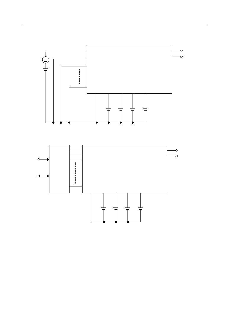
Measuring circuit 1
Measuring circuit 2
A
V
V
XT
XT
C1
C2
Crystal
32.768 kHz
C
12
V
SS
V
DD1
V
DD2
V
DD3
C
a
C
b
C
a
C
b
, C
12
R
OS
RT0
CS0
RI0
: 1 mF
: 0.1 mF
: 300 kW
: 10 kW/2 kW
: 820 pF
: 10 kW
OSC1
OSC2
R
OS
V
DD
RT0
CS0
RI0
RT0
CS0
IN0
OUTPUT
V
SS
V
DD1
V
DD2
V
DD3
(*2)
INPUT
(*1)
V
IH
V
IL
V
DD
A
15/37
° Semiconductor
MSM64P164
Measuring circuit 3
Measuring circuit 4
*1 Input logic circuit to determine the specified measuring conditions.
*2 Measured at the specified output pins.
*3 Measured at the specified input pins.
V
DD2
OUTPUT
V
SS
V
DD3
V
DD
(*3)
INPUT
V
DD1
A
OUTPUT
V
SS
V
DD2
V
DD3
V
DD
INPUT
(*3)
V
IH
V
IL
Waveform
Monitoring
V
DD1

16/37
° Semiconductor
MSM64P164
A/D Converter Characteristics
*
Kfx is the ratio of the oscillation frequency by a sensor resistor to the oscillation frequency
by a reference resistor in the same condition.
Parameter
Symbol
Condition
Min.
Typ.
Max.
Unit
Measur-
ing
Circuit
Resistor
for Oscillation
CS0, CT0, CS1 740 pF
2.0
kW
Input Current
Limiting Resistor
Oscillation
Frequency
RS∑RT Oscillation
Frequency Ratio
(*)
RI0, RI1
f
OSC1
f
OSC2
f
OSC3
Kf1
Kf2
Kf3
Resistor for oscillation = 2 kW
Resistor for oscillation = 10 kW
Resistor for oscillation = 200 kW
RT0, RT0-1, RT1 = 2 kW
RT0, RT0-1, RT1 = 10 kW
RT0, RT0-1, RT1 = 200 kW
1.0
165
41.8
2.55
3.89
0.990
0.0561
10
221
52.2
3.04
4.18
1.0
0.0584
256
60.6
3.53
4.35
1.010
0.0637
kW
kHz
kHz
5
RS0, RS1,
RT0,
RT0-1,
RT1
--
kHz
--
--
--
--
--
--
(V
SS
= 0 V, V
DD
= 1.5 V, Ta = 0 to +65∞C unless otherwise specified)
Kfx =
f
OSCX
(RS0≠CS0 Oscillation)
f
OSCX
(RT0≠CS0 Oscillation)
(x = 1, 2, 3)
f
OSCX
(RT0-1≠CS0 Oscillation)
f
OSCX
(RS0≠CS0 Oscillation)
f
OSCX
(RT1≠CS1 Oscillation)
f
OSCX
(RS1≠CS1 Oscillation)
,
,

17/37
° Semiconductor
MSM64P164
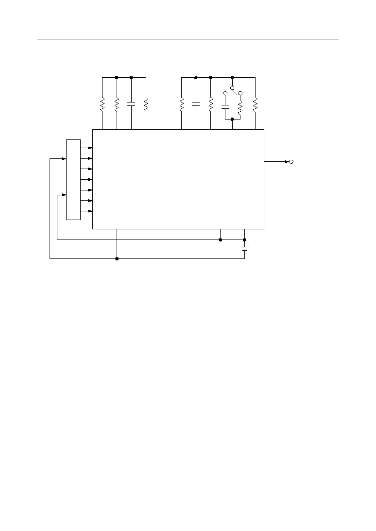
Measuring circuit 5
D. U. T.
V
DD1
V
DD
V
SS
RT0, RT0-1, RT1 = 2 kW/10 kW/200 kW
RS0, RS1 = 10 kW
RI0, RI1 = 10 kW
CS0, CT0, CS1 = 820 pF
RESET
RT1
RT1
IN1
CS1
RS1
RS1
CS1
RI1
RI0
IN0
CRT0
RS0
CS0
CS0
RS0
CT0
RT0-1
RT0
RT0
P4.3
TST1
TST2
P0.0
P0.1
P0.2
P0.3
(CROSC1)
(CROSC0)
Oscillation Mode Specified
Frequency
Measurement
(f
OSCX
)
18/37
° Semiconductor
MSM64P164
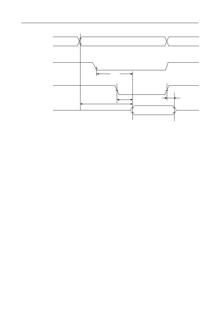
AC Characteristics (Serial Interface)
--
15
50
ns
SCLK Input Fall Time
t
f
SCLK Input "H" Level Pulse Width
t
CWH
m
s
--
SCLK Input Cycle Time
t
CYC
m
s
--
t
CYC2(O)
m
s
--
m
s
--
0.8
--
2.0
--
2.5
--
SOUT Output Delay Time
t
DDR
m
s
0.4
--
--
0.5
--
m
s
30.5
--
CPU is operating at 32.768 kHz.
--
--
CPU is operating at 400 kHz.
C
l
= 10 pF
--
Parameter
Symbol
Condition
Unit
Max.
Typ.
Min.
t
CYC1(O)
0.8
--
--
m
s
--
t
DS
t
DH
--
--
15
50
ns
SCLK Input Rise Time
t
r
--
0.8
--
--
m
s
SCLK Input "L" Level Pulse Width
t
CWL
--
SCLK Output Cycle Time
SCLK Output Cycle Time
SIN Input Setup Time
SIN Input Hold TIme
(V
SS
= 0 V, V
DD1
= 1.5 V, V
DD
= 5 V, Ta = 0 to +65∞C)
--
SCLK
(P4.2)
SOUT
(P4.0)
SIN
(P3.3)
5 V
5 V
5 V
t
CYC
t
CWH
t
CWL
t
DDR
t
DDR
t
DH
t
DS
t
DS
t
r
t
f
("H" level = 4 V, "L" level = 1 V)
19/37
° Semiconductor
MSM64P164
ABSOLUTE MAXIMUM RATINGS (3.0 V Spec.)
RECOMMENDED OPERATING CONDITIONS (3.0 V Spec.)
Parameter
Power Supply Voltage 1
Symbol
Condition
Rating
Unit
V
DD1
Ta = 25∞C
≠0.3 to +2.0
V
Power Supply Voltage 2
V
DD2
Ta = 25∞C
≠0.3 to +4.0
V
Power Supply Voltage 3
V
DD3
Ta = 25∞C
≠0.3 to +5.5
V
Power Supply Voltage 4
V
DD
Ta = 25∞C
≠0.3 to +5.5
V
Input Voltage 1
V
IN1
V
DD2
input, Ta = 25∞C
≠0.3 to V
DD2
+ 0.3
V
Input Voltage 2
V
IN2
V
DD
input, Ta = 25∞C
≠0.3 to V
DD
+ 0.3
V
Output Voltage 1
V
OUT1
V
DD2
output, Ta = 25∞C
≠0.3 to V
DD2
+ 0.3
V
Output Voltage 2
V
OUT2
V
DD3
output Ta = 25∞C
≠0.3 to V
DD3
+ 0.3
V
Output Voltage 3
V
OUT3
V
DD
output, Ta = 25∞C
≠0.3 to V
DD
+ 0.3
V
(V
SS
= 0 V)
Storage Temperature
T
STG
--
≠55 to +150
∞C
Parameter
Symbol
Condition
Range
Unit
(V
SS
= 0 V)
Operating Temperature
T
op
--
0 to +65
∞C
Operating Voltage
V
DD2
--
2.7 to 3.5
V
V
DD
--
V
DD2
to 5.25
V
External 400kHz RC Oscillator
Resistance
R
OS
--
90 to 500
kW
Crystal Oscillation Frequency
f
XT
--
30 to 66
kHz
20/37
° Semiconductor
MSM64P164
ELECTRICAL CHARACTERISTICS (3.0 V Spec.)
DC Characteristics
Parameter
+100%
≠20%
Symbol
Condition
Min.
Typ.
Max.
Unit
Measuring
Circuit
V
DD1
Voltage
V
DD1
C
a
, C
b
, C
12
= 0.1 mF
1.3
1.5
1.7
V
V
DD3
Voltage
V
DD3
C
a
, C
b
, C
12
= 0.1 mF
4.3
4.5
4.7
V
Crystal Oscillation
Start Voltage
V
STA
Oscillation start time:
within 5 seconds
2.7
--
--
V
Crystal Oscillation
Hold Voltage
V
HOLD
--
2.7
--
--
V
Crystal Oscillation
Stop Detection Time
T
STOP
--
0.1
--
1000
ms
Internal Crystal
Oscillator Capacitance
C
G
--
10
15
20
pF
External Crystal
Oscillator Capacitance
C
GEX
When external C
G
used
10
--
30
pF
Internal Crystal
Oscillator Capacitance
C
D
--
10
15
20
pF
Internal 400k RC
Oscillator Capacitance
C
OS
--
8
12
16
pF
400k RC Oscillation
Frequency
f
OSC
External resistor R
OS
= 100 kW
V
DD2
= 2.7 to 3.5 V
300
400
620
kHz
POR Generation
Voltage
V
POR1
When V
DD2
is between V
POR1
and 3.0 V
0
--
0.7
V
POR Non-generation
Voltage
V
POR2
No POR when V
DD2
is between
V
POR2
and 3.0 V
2.7
--
3
V
+100%
≠20%
1
(V
SS
= 0 V, V
DD2
= V
DD
= 3.0 V, Ta = 0 to +65∞C unless otherwise specified)
Notes: 1. "POR" denotes Power On Reset.
2. "T
STOP
" indicates that if the crystal oscillator stops over the value of T
STOP
, the
system reset occurs.
21/37
° Semiconductor
MSM64P164
DC Characteristics (continued)
Parameter
Symbol
Condition
Min.
Typ.
Max.
Unit
Measuring
Circuit
Supply Current 1
I
DD1
--
1.0
4.0
m
A
Supply Current 2
I
DD2
Supply Current 3
I
DD3
CPU in operating state
(400k RC oscillation in operation)
--
220
450
m
A
Supply Current 4
I
DD4
Serial transfer,
f
SCK
= 300 kHz,
CPU in operating state
(400k RC oscillation halt)
Supply Current 5
I
DD5
CPU in halt state
(400k RC oscillation
halt), RC oscillator for
A/D converter is in
operating state
--
300
450
m
A
1
(V
SS
= 0 V, V
DD2
= V
DD
= 3.0 V, Ta = 0 to +65∞C unless otherwise specified)
CPU in operating state
(400k RC oscillation halt)
CPU in halt state
(400k RC oscillation halt)
RT0 = 10 kW
RT0 = 2 kW
--
25
50
m
A
--
30
60
m
A
--
1300
2000
m
A
22/37
° Semiconductor
MSM64P164
DC Characteristics (continued)
Parameter
(Pin Name)
Symbol
Condition
Unit
Measuring
Circuit
Output Current 1
(P1.0)
I
OH1
V
OH1
= V
DD
≠ 0.5 V
Min.
Typ.
Max.
≠6.0
≠2.0
≠0.7
mA
I
OL1
V
OL1
= 0.5 V
3.0
8.0
25
mA
Output Current 2
(P1.1 to P1.3)
(P2.0 to P2.3)
(P3.0 to P3.3)
(P4.0 to P4.3)
I
OH2
≠6.0
≠2.0
≠0.7
mA
I
OL2
V
OL2
= 0.5 V
0.7
2.0
6.0
mA
2
Output Current 3
(BD)
I
OH3
V
OH3
= V
DD2
≠ 0.7 V
≠6.0
≠2.0
≠0.7
mA
I
OL3
V
OL3
= 0.7 V
0.7
2.0
6.0
mA
Output Current 4
(RT0, RT1, RS0, RS1,
CRT0, CS0, CS1)
I
OH4
V
OH4
= V
DD2
≠ 0.1 V
≠2.5
≠1.3
≠0.7
mA
I
OL4
V
OL4
= 0.1 V
0.7
1.3
2.5
mA
Output Current 5
(When L26 to L33 are
configured as output
ports)
I
OH5
V
OH5
= V
DD
≠ 0.5 V
≠1.5
≠0.6
≠0.15
mA
I
OL5S
V
DD
= 5 V, V
OL5S
= 0.5 V
0.2
0.7
2.0
mA
Output Current 6
(OSC2)
I
OH6
V
OH6
= V
DD2
≠ 0.5 V
≠6.0
≠2.0
≠0.7
mA
I
OL6
V
OL6
= 0.5 V
0.7
2.0
6.0
mA
I
OH7
V
OH7
= V
DD3
≠ 0.2 V
--
--
≠4.0
m
A
I
OMH7
V
OMH7
= V
DD2
+ 0.2 V
4.0
--
--
m
A
I
OMH7S
V
OMH7S
= V
DD2
≠ 0.2 V
--
--
≠4.0
m
A
I
OML7
V
OML7
= V
DD1
+ 0.2 V
4.0
--
--
m
A
I
OML7S
V
OML7S
= V
DD1
≠ 0.2 V
--
--
≠4.0
m
A
I
OL7
V
OL7
= 0.2 V
4.0
--
--
m
A
Output Current 7
(L0 to L33)
Output Leakage Current
(P1.0 to P1.3)
(P2.0 to P2.3)
(P3.0 to P3.3)
(P4.0 to P4.3)
(RT0, RT1, RS0, RS1,
CRT0, CS0, CS1)
I
OOH
V
OH
= V
DD2
--
--
0.3
m
A
I
OOL
V
OL
= V
SS
≠0.3
--
--
m
A
V
OH2
= V
DD
≠ 0.5 V
(V
DD3
level)
(V
DD2
level)
(V
DD2
level)
(V
DD1
level)
(V
DD1
level)
(V
SS
level)
I
OL1S
V
DD
= 5 V, V
OL1
= 0.5 V
4.0
12
36
mA
I
OL2S
V
DD
= 5 V, V
OL2
= 0.5 V
1.0
3.0
9.0
mA
I
OL5
V
OL5
= 0.5 V
0.15
0.6
1.5
mA
(V
SS
= 0 V, V
DD1
= 1.5 V, V
DD2
= V
DD
= 3.0 V, V
DD3
= 4.5 V,
Ta = 0 to +65∞C unless otherwise specified)
23/37
° Semiconductor
MSM64P164
DC Characteristics (continued)
Parameter
(Pin Name)
Symbol
Condition
Unit
Measuring
Circuit
Input Current 1
(P0.0 to P0.3)
(P2.0 to P2.3)
(P3.0 to P3.3)
(P4.0 to P4.3)
I
IH1
V
IH1
= V
DD
(when pulled down)
Min.
Typ.
Max.
30
90
300
m
A
I
IL1
V
IL1
= V
SS
(when pulled up)
≠300
≠90
≠30
m
A
3
I
IH1Z
V
IH1
= V
DD
(in a high impedance state)
0
--
1.0
m
A
I
IL1Z
V
IL1
= V
SS
(in a high impedance state)
≠1.0
--
0
m
A
I
IH2
V
IH2
= V
DD2
(when pulled down)
30
90
300
m
A
I
IH2Z
V
IH2
= V
DD2
(in a high impedance state)
0
--
1.0
m
A
I
IL2Z
V
IL2
= V
SS2
(in a high impedance state)
≠1.0
--
0
m
A
I
IL3
V
IL3
= V
SS
(when pulled up)
≠300
≠110
≠10
m
A
I
IH3Z
V
IH3
= V
DD2
(in a high impedance state)
0
--
1.0
m
A
I
IL3Z
V
IL3
= V
SS
(in a high impedance state)
≠1.0
--
0
m
A
I
IH4
V
IH4
= V
DD2
0
--
1.0
m
A
I
IL4
V
IL4
= V
SS
≠3.0
≠1.5
≠0.75
mA
V
IH1
--
2.4
--
3.0
V
V
IL1
--
0
--
0.6
V
V
IH2
--
2.4
--
3.0
V
V
IL2
--
0
--
0.6
V
V
IH3
--
2.4
--
3.0
V
V
IL3
--
0
--
0.6
V
Input Current 2
(IN0, IN1)
Input Current 3
(OSC1)
Input Current 4
(RESET, TST1, TST2)
Input Voltage 1
(P0.0 to P0.3)
(P2.0 to P2.3)
(P3.0 to P3.3)
(P4.0 to P4.3)
Input Voltage 2
(IN0, IN1, OSC1)
Input Voltage 3
(RESET, TST1, TST2)
4
I
IH1S
V
IH1
= V
DD
= 5 V (when pulled down)
80
250
800
m
A
I
IL1S
V
IL1
= V
SS
, V
DD
= 5 V (when pulled up)
≠800
≠250
≠80
m
A
V
IH1S
4.0
--
5.0
V
V
IL1S
0
--
1.0
V
V
DD
= 5 V
V
DD
= 5 V
(V
SS
= 0 V, V
DD1
= 1.5 V, V
DD2
= V
DD
= 3.0 V, V
DD3
= 4.5 V,
Ta = 0 to +65∞C unless otherwise specified)

24/37
° Semiconductor
MSM64P164
DC Characteristics (continued)
Parameter
(Pin Name)
Symbol
Condition
Unit
Measuring
Circuit
Hysteresis Width
(P0.0 to P0.3)
(P2.0 to P2.3)
(P3.0 to P3.3)
(P4.0 to P4.3)
D
V
T1S
V
DD
= 5 V
Min.
Typ.
Max.
0.25
1.0
1.5
V
4
D
V
T2
--
0.2
0.5
1.0
V
C
IN
--
--
--
5.0
pF
Hysteresis Width
(RESET, TST1, TST2)
Input Pin Capacitance
(P0.0 to P0.3)
(P2.0 to P2.3)
(P3.0 to P3.3)
(P4.0 to P4.3)
1
D
V
T1
--
0.2
0.5
1.0
V
(V
SS
= 0 V, V
DD1
= 1.5 V, V
DD2
= V
DD
= 3.0 V, V
DD3
= 4.5 V,
Ta = 0 to +65∞C unless otherwise specified)
25/37
° Semiconductor
MSM64P164
Measuring circuit 1
Measuring circuit 2
A
V
V
XT
XT
C1
C2
Crystal
32.768 kHz
C
12
V
SS
V
DD2
V
DD1
V
DD3
C
a
C
b
C
a
, C
b
, C
12
R
OS
RT0
CS0
RI0
: 0.1 mF
: 100 kW
: 10 kW/2 kW
: 820 pF
: 10 kW
OSC1
OSC2
R
OS
V
DD
RT0
CS0
RI0
RT0
CS0
IN0
OUTPUT
V
SS
V
DD1
V
DD2
V
DD3
(*2)
INPUT
(*1)
V
IH
V
IL
V
DD
A
26/37
° Semiconductor
MSM64P164
Measuring circuit 3
Measuring circuit 4
*1 Input logic circuit to determine the specified measuring conditions.
*2 Measured at the specified output pins.
*3 Measured at the specified input pins.
V
DD2
OUTPUT
V
SS
V
DD3
V
DD
(*3)
INPUT
V
DD1
A
OUTPUT
V
SS
V
DD2
V
DD3
V
DD
INPUT
(*3)
V
IH
V
IL
Waveform
Monitoring
V
DD1
27/37
° Semiconductor
MSM64P164
A/D Converter Characteristics
Parameter
Symbol
Condition
Min.
Typ.
Max.
Unit
Measur-
ing
Circuit
Resistor
for Oscillation
CS0, CT0, CS1 740 pF
1.0
kW
Input Current
Limiting Resistor
Oscillation
Frequency
RS∑RT Oscillation
Frequency Ratio
(*)
RI0, RI1
f
OSC1
f
OSC2
f
OSC3
Kf1
Kf2
Kf3
Resistor for oscillation = 2 kW
Resistor for oscillation = 10 kW
Resistor for oscillation = 200 kW
RT0, RT0-1, RT1 = 2 kW
RT0, RT0-1, RT1 = 10 kW
RT0, RT0-1, RT1 = 200 kW
1.0
200
46.5
2.79
4.115
0.990
0.0573
10
239
55.4
3.32
4.22
1.0
0.0616
277
64.3
3.85
4.326
1.010
0.0659
kW
kHz
kHz
5
Kfx =
f
OSCX
(RS0≠CS0 Oscillation)
f
OSCX
(RT0≠CS0 Oscillation)
(x = 1, 2, 3)
RS0, RS1,
RT0,
RT0-1,
RT1
--
kHz
--
--
--
--
--
--
f
OSCX
(RT0-1≠CS0 Oscillation)
f
OSCX
(RS0≠CS0 Oscillation)
f
OSCX
(RT1≠CS1 Oscillation)
f
OSCX
(RS1≠CS1 Oscillation)
,
,
(V
SS
= 0 V, V
DD2
= V
DD
= 3.0 V, Ta = 0 to +65∞C unless otherwise specified)
*
Kfx is the ratio of the oscillation frequency by a sensor resistor to the oscillation frequency
by a reference resistor in the same condition.
28/37
° Semiconductor
MSM64P164
Measuring circuit 5
D. U. T.
V
DD2
V
DD
V
SS
RT0, RT0-1, RT1 = 2 kW/10 kW/200 kW
RS0, RS1 = 10 kW
RI0, RI1 = 10 kW
CS0, CT0, CS1 = 820 pF
RESET
RT1
RT1
IN1
CS1
RS1
RS1
CS1
RI1
RI0
IN0
CRT0
RS0
CS0
CS0
RS0
CT0
RT0-1
RT0
RT0
P4.3
TST1
TST2
P0.0
P0.1
P0.2
P0.3
(CROSC1)
(CROSC0)
Oscillation Mode Specified
Frequency
Measurement
(f
OSCX
)

29/37
° Semiconductor
MSM64P164
AC Characteristics (Serial Interface)
("H" level = 4 V, "L" level = 1 V)
--
15
50
ns
SCLK Input Fall Time
t
f
SCLK Input "H" Level Pulse Width
t
CWH
m
s
--
SCLK Input Cycle Time
t
CYC
m
s
--
t
CYC2(O)
m
s
--
m
s
--
0.8
--
2.0
--
2.5
--
SOUT Output Delay Time
t
DDR
m
s
0.4
--
--
0.5
--
m
s
30.5
--
CPU is operating at 32.768 kHz.
--
--
CPU is operating at 400 kHz.
C
l
= 10 pF
--
Parameter
Symbol
Condition
Unit
Max.
Typ.
Min.
t
CYC1(O)
0.8
--
--
m
s
--
t
DS
t
DH
--
--
15
50
ns
SCLK Input Rise Time
t
r
--
0.8
--
--
m
s
SCLK Input "L" Level Pulse Width
t
CWL
--
SCLK Output Cycle Time
SCLK Output Cycle Time
SIN Input Setup Time
SIN Input Hold TIme
(V
SS
= 0 V, V
DD2
= 3 V, V
DD
= 5 V, Ta = 0 to +65∞C)
--
SCLK
(P4.2)
SOUT
(P4.0)
SIN
(P3.3)
5 V
5 V
5 V
t
CYC
t
CWH
t
CWL
t
DDR
t
DDR
t
DH
t
DS
t
DS
t
r
t
f

30/37
° Semiconductor
MSM64P164
ABSOLUTE MAXIMUM RATINGS (1.5 V/3.0 V Spec., PROM Mode)
RECOMMENDED OPERATING CONDITIONS (1.5 V/3.0 V Spec., PROM Mode)
Storage Temperature
T
STG
--
≠55 to +150
∞C
Parameter
PROM Power Supply Voltage
Symbol
Condition
Rating
Unit
V
CC
V
CC
= V
DD1
= V
DD2
, Ta = 25∞C
≠0.3 to +6.7
V
Program Voltage
V
PP
Ta = 25∞C
≠0.3 to +14.0
V
PROM Input Voltage
V
I
V
CC
input, Ta = 25∞C
≠0.3 to V
CC
+ 0.3
V
PROM Output Voltage
V
O
V
CC
output, Ta = 25∞C
≠0.3 to V
CC
+ 0.3
V
(V
SS
= 0 V)
Parameter
Symbol
Condition
Range
Unit
(V
SS
= 0 V)
Operating Temperature
T
op
--
0 to 65
∞C
V
CC
Power Supply Voltage
V
CC
V
CC
= V
DD1
= V
DD2
4.75 to 5.25
V
V
PP
Power Supply Voltage
V
PP
During read
4.75 to 5.25
V
During write
12.0 to 13.0
V
Input Voltage
V
IH
V
CC
= V
DD1
= V
DD2
4 to V
CC
V
V
IL
--
0 to 1
V
31/37
° Semiconductor
MSM64P164
ELECTRICAL CHARACTERISTICS (1.5 V/3.0 V Spec., PROM Mode)
(1) Read Operation
DC Characteristics
AC Characteristics
Max.
Typ.
Min.
Symbol
Condition
Unit
Parameter
I
CC1
mA
35
--
--
V
CC
= V
DD1
= V
DD2
CE = V
IH
V
CC
Power Supply Current
(Standby)
I
CC2
mA
100
--
--
V
CC
= V
DD1
= V
DD2
CE = V
IL
V
CC
Power Supply Current
(Operating)
V
IH
V
V
CC
--
4.0
V
CC
= V
DD1
= V
DD2
Input Voltage
V
IL
1.0
--
0
--
I
OH
≠0.7
≠2.0
Output Current
I
OL
0.7
0.2
V
OL
= 0.5 V
≠0.2
2.0
V
mA
mA
V
CC
= V
DD1
= V
DD2
V
OH
= V
CC
≠ 0.5 V
(V
DD1
= V
DD2
= V
PP
= 5 V ±5%, Ta = 25∞C ±5∞C, unless otherwise specified)
Max.
Typ.
Min.
Symbol
Condition
Unit
Parameter
t
ACC
ns
120
--
--
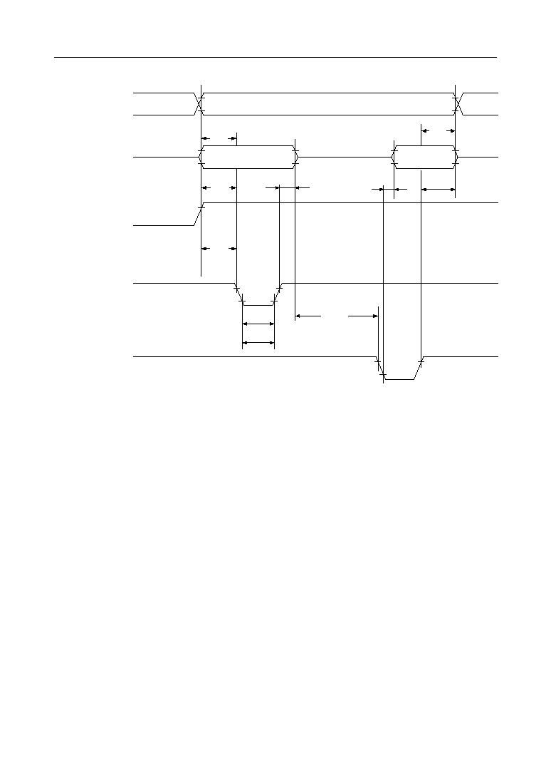
Address Access Time
t
CE
ns
120
--
--
CE Access Time
t
OE
ns
50
--
--
OE Access Time
t
DF
40
--
0
Output Disable Time
ns
OE = CE = V
IL
OE = V
IL
CE = V
IL
CE = V
IL
(V
CC
= 5 V ±5%, V
PP
= V
CC
, Ta = 25∞C ±5∞C, unless otherwise specified)
Measurement conditions:
Input pulse level ...................... 0.45 V to 4.55 V
Input rise/fall time ................. 5 ns
Threshold level ........................ input 0.8 V, 2 V/output 0.8 V, 2 V
32/37
° Semiconductor
MSM64P164
t
CE
Address Input
CE
OE
t
DF
t
OE
Data Output
t
ACC
33/37
° Semiconductor
MSM64P164
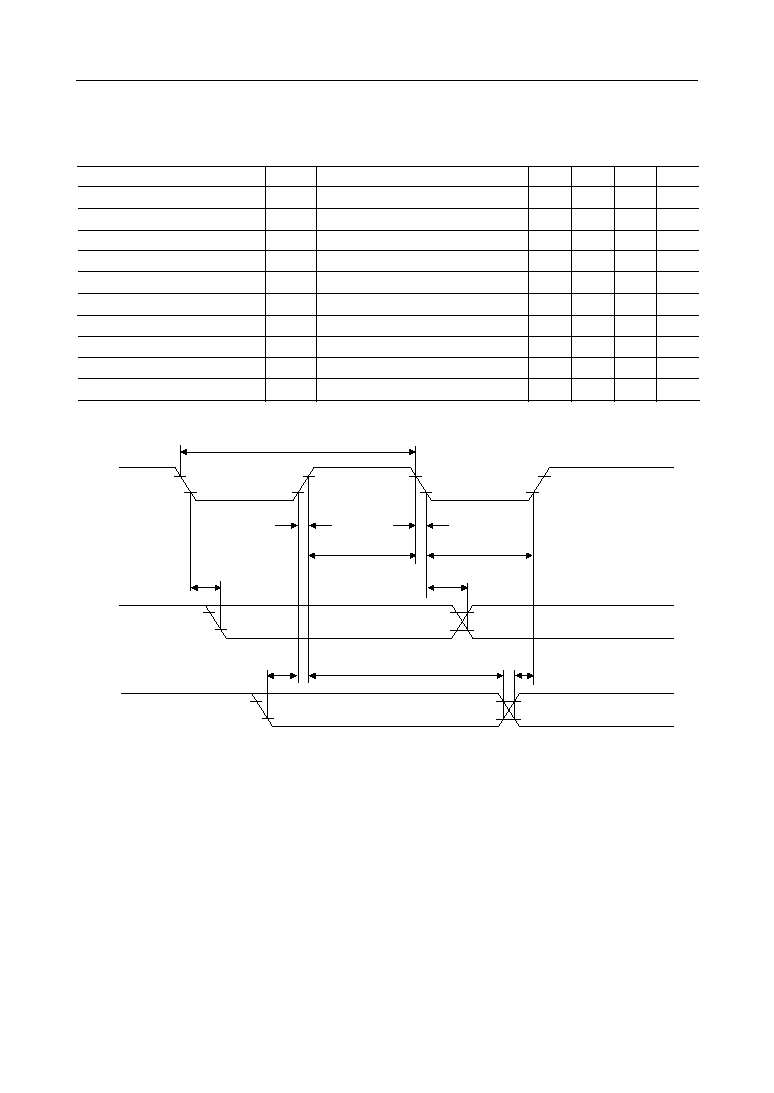
(2) Write Operation
DC Characteristics
AC Characteristics
Measurement conditions:
Input pulse level ...................... 0.45 V to 4.55 V
Input rise/fall time ................. less than 20 ns
Threshold level ........................ input 0.8 V, 2 V/output 0.8 V, 2 V
Max.
Typ.
Min.
Symbol
Condition
Unit
Parameter
I
PP
mA
50
--
--
CE = V
IL
V
PP
Power Supply Current
I
CC
mA
100
--
--
V
CC
= V
DD1
= V
DD2
V
CC
Power Supply Current
V
IH
V
V
CC
--
4.0
V
CC
= V
DD1
= V
DD2
Input Voltage
V
IL
1.0
--
0
--
I
OH
≠0.7
≠2.0
Output Current
I
OL
0.7
0.2
V
OL
= 0.5 V
≠0.2
2.0
V
mA
mA
V
CC
= V
DD1
= V
DD2
V
OH
= V
CC
≠ 0.5 V
(V
SS
= 0 V, V
DD1
= V
DD2
= 5 V ±5%, V
PP
= 12.5 V ±0.5 V, Ta = 25∞C ±5∞C, unless otherwise specified)
Max.
Typ.
Min.
Symbol
Condition
Unit
Parameter
t
AS
m
s
--
--
2.0
Address Setup Time
t
OES
m
s
--
--
2.0
OE Setup Time
t
DS
m
s
--
--
2.0
Data Setup Time
t
AH
--
--
0
Address Hold Time
m
s
--
t
DH
m
s
--
--
2.0
Data Hold Time
t
DFP
ns
130
--
0
OE Output Floating Delay Time
t
VS
m
s
--
--
2.0
V
PP
Power Source Setup Time
t
PW
1.05
1.0
0.95
Initial Program Pulse Width
ms
--
--
--
--
--
--
t
OPW
ms
78.75
--
2.85
Additional Program Pulse Width
t
OE
ns
150
--
--
V
DD1
= V
DD2
6 V ±0.25 V
--
OE Output Effective Delay Time
V
DD1
= V
DD2
6 V ±0.25 V
(V
SS
= 0 V, V
DD1
= V
DD2
= 5 V ±5%, V
PP
= 12.5 V ±0.5 V, Ta = 25∞C ±5∞C, unless otherwise specified)
34/37
° Semiconductor
MSM64P164
Data Input-Output
Address N
Data Input
Data Output
t
AS
t
DS
t
DH
t
VS
t
AH
t
OE
t
DFP
t
PW
t
OPW
t
OES
Address Input
V
PP
CE
OE
35/37
° Semiconductor
MSM64P164
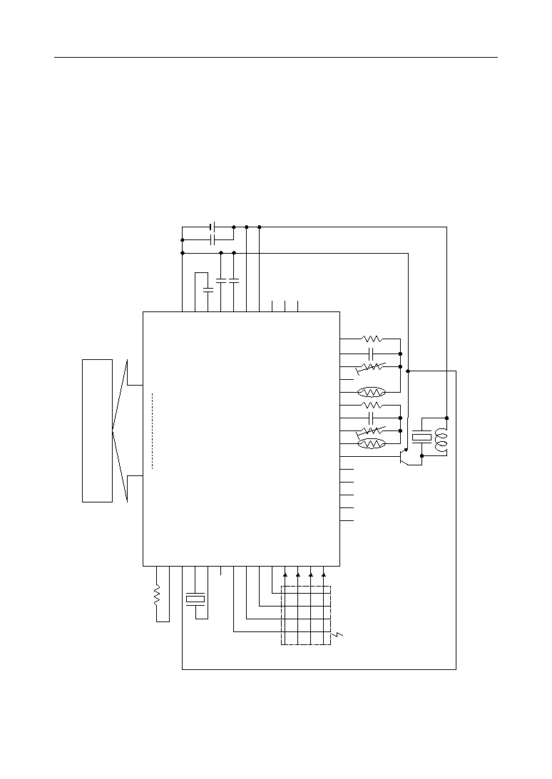
OSC2
OSC1
V
SS
XT
XT
RESET
P1.0
P1.1
P1.2
P1.3
P0.0
P0.1
P0.2
P0.3
IN0
CS0
RS0
CRT0
RT0
IN1
CS1
RS1
RT1
BD
P4.3
P4.2
P4.1
P4.0
P3.3
V
SS
C2
C1
V
DD3
V
DD2
V
DD
V
DD1
V
PP
TST2
TST1
R
OS
32.768 kHz
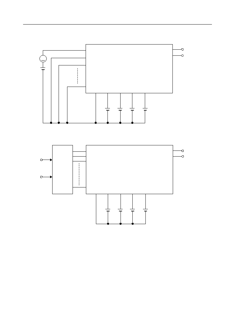
Switch matrix
(4 • 4)
RS1
RT1
CS1 RI1
RT0
RS0
CS0
RI0
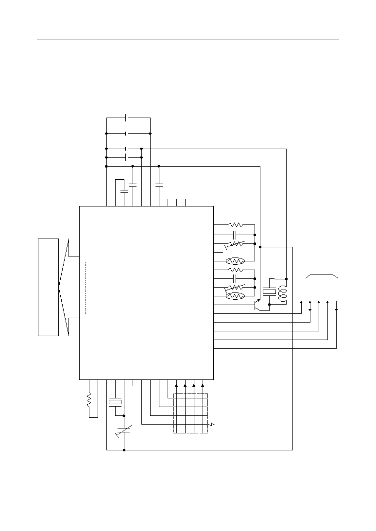
MSM64P164-xxx
(1.5 V spec.)
Buzzer
C
12
C
b
C1
1.5 V
*
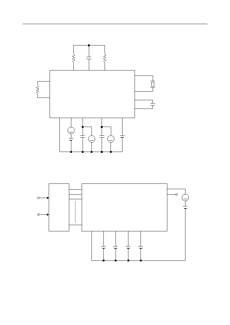
∑ Without 5 V interface
∑ Temperature
measurement
by two thermistors
∑ C
G
of crystal oscillator :
Internal
* Polarity is reversed when
compared to mask ROM
version of this device.
L33
L0
L C D
C
a
Crystal
APPLICATION CIRCUITS
1.5 V Spec. Application Circuit
36/37
° Semiconductor
MSM64P164
OSC2
OSC1
V
SS
XT
XT
RESET
P1.0
P1.1
P1.2
P1.3
P0.0
P0.1
P0.2
P0.3
IN0
CS0
RS0
CRT0
RT0
IN1
CS1
RS1
RT1
BD
P4.3
P4.2
P4.1
P4.0
P3.3
V
SS
C2
C1
V
DD3
V
DD2
V
DD
V
DD1
V
PP
TST2
TST1
R
OS
32.768 kHz
C
GEX
Switch matrix
(4 • 4)
RS1
RT1
CS1
RI1
RT0
RS0
CS0
RI0
MSM64P164-xxx
(3 V spec.)
OSC monitor
SCLK
SPR
SOUT
SIN
To the serial communication interface
(5 V (V
DD
) system)
Buzzer
C
12
C
b
C
a
C2
3 V
*
5 V
*
C
S
∑ With 5 V interface
∑ Temperature measurement
by two thermistors
∑ C
GEX
of crystal
oscillator : External
* Polarity is reversed when
compared to mask ROM
version of this device.
L33
L0
L C D
Crystal
APPLICATION CIRCUITS (continued)
3.0 V Spec. Application Circuit
37/37
° Semiconductor
MSM64P164
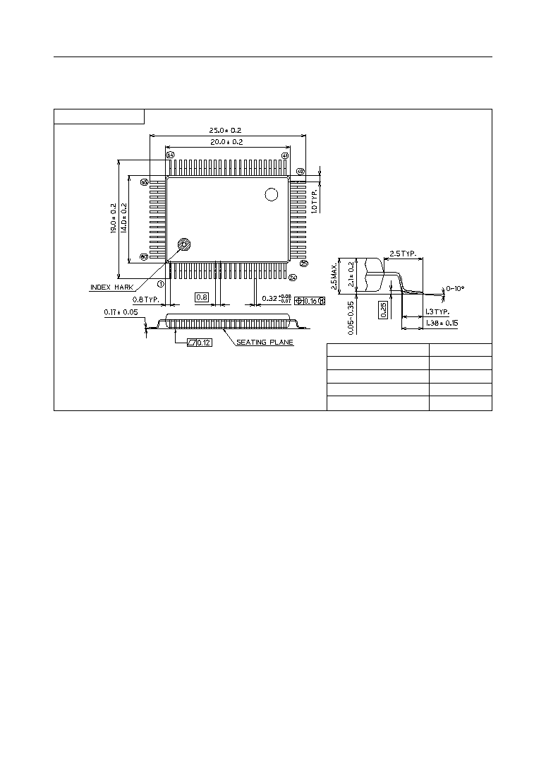
(Unit : mm)
Notes for Mounting the Surface Mount Type Package
The SOP, QFP, TSOP, SOJ, QFJ (PLCC), SHP and BGA are surface mount type packages, which
are very susceptible to heat in reflow mounting and humidity absorbed in storage.
Therefore, before you perform reflow mounting, contact Oki's responsible sales person for the
product name, package name, pin number, package code and desired mounting conditions
(reflow method, temperature and times).
QFP80-P-1420-0.80-BK
Package material
Lead frame material
Pin treatment
Solder plate thickness
Package weight (g)
Epoxy resin
42 alloy
Solder plating
5 mm or more
1.27 TYP.
Mirror finish
PACKAGE DIMENSIONS