 | –≠–ª–µ–∫—Ç—Ä–æ–Ω–Ω—ã–π –∫–æ–º–ø–æ–Ω–µ–Ω—Ç: MSM65352 | –°–∫–∞—á–∞—Ç—å:  PDF PDF  ZIP ZIP |

1/15
° Semiconductor
MSM65352/65352B
° Semiconductor
MSM65352/65352B
8-Bit Microcontroller with 4-Bit A/D Converter (with LCD Driver)
GENERAL DESCRIPTION
The MSM65352 is a high performance 8-bit microcontroller that employs OKI original CPU core,
the nX-8/50. The MSM65352 includes 8K-byte program memory, 256-byte data memory, LCD
driver, timer, serial I/O and 4-bit A/D converter. Also available is the MSM65352B, which has four
LCD outputs in place of four output ports. Also available are the MSM65P352 and MSM65P352B,
which replace the on-chip program memory with one-time PROM.
FEATURES
∑ Operating range
Operating voltage
:
2.7V to 5.5V
Operating temperature
:
≠20
∞
C to +70
∞
C
Operating frequency:
High speed side
:
0 to 10MHz (@V
DD
=5V
±
10%)
(dual clock)
:
0 to 5MHz (@V
DD
=2.7V to 5.5V)
Low speed side
:
32.768kHz (@V
DD
=2.7V to 5.5V)
∑ Current consumption (Typ.): High speed side
:
5mA (@5MHz, V
DD
=3V)
20mA (@10MHz, V
DD
=5V)
1.5mA (@5MHz, V
DD
=3V, halt mode)
Low speed side
:
45mA (@32.768kHz, V
DD
=3V)
4mA (@V
DD
=3V, stop mode)
∑ Minimum instruction execution time :
400ns (@10MHz), 800ns (@5MHz)
∑ CPU core
:
8-bit CPU core nX-8/50
∑ General memory space
:
8K-byte program memory
∑ Local memory space
:
256-byte data memory + SFR
∑ LCD driver
:
16 • 4 (MSM65352), 20 • 4 (MSM65352B)
∑ I/O port
:
5 ports, 31 bits (MSM65352)
4 ports, 27 bits (MSM65352B)
Input-output port
:
2 ports • 8 bits, 1 port • 1 bit
Input port
:
1 port • 1 bit
1 port • 4 bits (Only for MSM65352)
Output port
:
1 port • 8 bits, 1 port • 1 bit
∑ Timer
:
8-bit auto-reload timer • 2
Watchdog timer • 1
Watch timer
(counter clock is fixed at XT=32.768kHz)
∑ Counter
:
Time base counter • 1 (14 bits)
∑ Serial I/O
:
1ch, clock sync • 1
∑ A/D converter
:
4-bit • 8-ch, with reference current cutoff function
∑ Remote control input circuit
:
Receives signal in 32kHz/5MHz/10MHz operations
∑ Interrupt source
:
9 sources
∑ Package:
64-pin plastic QFP (QFP64-P-1414-0.80-BK)(Product name: MSM65352-•••GS-BK,
MSM65352B-•••GS-BK)
••• indicates the code number.
E2E1019-27-Y3
This version: Jan. 1998
Previous version: Nov. 1996

2/15
° Semiconductor
MSM65352/65352B
∑ Others
:
CPU clock can be an OSC, half-OSC, or XT clock.
Time base counter can be selected with 1/4n of a
CPU clock (n=1 to 8).
3/15
° Semiconductor
MSM65352/65352B
BLOCK DIAGRAM
V
DD
GND
RAM
(256 bytes)
TBC
WDT
8-bit TIMER • 2
T1OUT*
T0CK*
GATE*
SFTO1*
SFTI1*
SFTCK1*
INTERRUPT CONT.
INT0*
INT1*
REMOTE CONT.
RMCIN*
BUS
CONT.
ROM
(8K bytes)
I/O PORT
P4**
4-bit A/D C
• 8ch
AGND
AV
DD
AI0-7*
GMAR
PC
LMAR
SP
PSW
BR
AR
ALU
IR
T/C
INST.
DEC.
OSC.
CONT.
XT
XT
OCS0
OSC1
RESET
HSTOP*
CLKOUT*
*Secondary function of each port.
**P4: for the MSM65352
SEG16-19: for the MSM65352B
SIO (SYNC MODE)
WATCH TIMER
LCD DRIVER
V
DDL
V
DD3
V
DD2
V
DD1
COM1
COM4
SEG0
SEG19**
SEG15
SEG16**
CPU CORE
P3
P2
P1
P0
4/15
° Semiconductor
MSM65352/65352B
PIN CONFIGURATION (TOP VIEW)
48
47
46
45
44
43
42
41
40
39
38
1
2
3
4
5
6
7
8
9
10
11
P0.7
P0.6
P0.5/CLKOUT
P0.4/INT1/GATE
P0.3/T0CK
P0.2/T1OUT
P0.1/HSTOP
P0.0/INT0
OSC0
OSC1
GND
SEG15
SEG14
SEG13
SEG12
SEG11
SEG10
SEG9
SEG8
SEG7
SEG6
SEG5
64
63
62
61
60
59
58
57
56
55
54
V
DD
P1.0
P1.1
P1.2
P1.3
P1.4/RMCIN
P1.5/SFTCK1
P1.6/SFTI1
P1.7/SFTO1
P2.0(IN)
P2.1(
TEST
)
17
18
19
20
21
22
23
24
25
26
27
P3.6/AI6
P3.5/AI5
P3.4/AI4
P3.3/AI3
P3.2/AI2
P3.1/AI1
P3.0/AI0
AV
DD
V
DD3
V
DD2
V
DD1
12
XT
13
XT
14
RESET
15
AGND
16
P3.7/AI7
28
V
DDL
29
COM1
30
COM2
31
COM3
32
COM4
37 SEG4
36 SEG3
35 SEG2
34 SEG1
33 SEG0
53
P2.2
52
P4.3****
54
P4.2***
50
P4.1**
49
P4.0*
* SEG16 for MSM65352B
** SEG17 for MSM65352B
*** SEG18 for MSM65352B
**** SEG19 for MSM65352B
64-Pin Plastic QFP
5/15
° Semiconductor
MSM65352/65352B
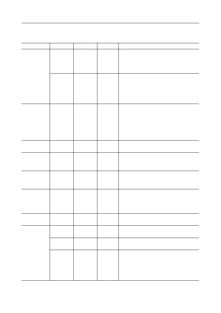
PIN DESCRIPTION
Basic Function
Function
Pin
Type
Description
64
--
Digital supply voltage (5V)
11
--
Digital ground
24
--
Analog supply voltage (5V)
15
--
Analog ground
27
--
Bias input for LCD driver
26
--
Bias input for LCD driver
25
--
Bias input for LCD driver
28
--
Ground for LCD driver bias
Power Supply
9
I
Oscillation input pin on the OSC side:
Connect to a quartz oscillator (ceramic resonator),
or input external clock.
10
O
Oscillation output pin on the OSC side:
Connect to a quartz oscillator (ceramic resonator).
When external clock is input to the OSC0 pin, the
OSC1 pin should be kept open.
13
I
Oscillation input pin on the XT side:
Connect to a quartz oscillator of 32.768kHz.
12
O
Oscillation output pin on the XT side:
Connect to a quartz oscillator of 32.768kHz.
Oscillation
Control
14
I
System reset input:
When this pin is set to the "L" level, the internal
status is initialized to start execution of
instructions from address 0040H. The input is
pulled up to V
DD
with an internal pull-up resistor.
Symbol
V
DD
GND
AV
DD
AGND
V
DD1
V
DD2
V
DD3
V
DDL
OSC0
OSC1
XT
XT
RESET
6/15
° Semiconductor
MSM65352/65352B
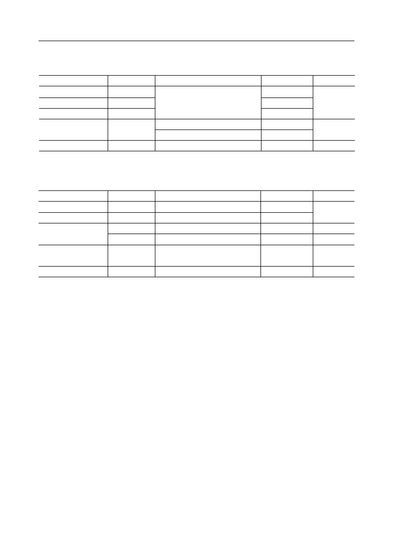
Function
Pin
Type
Description
8-bit Input-output port (port 0):
Each of bits 0 to 7 is configured to be an input or
an output by the direction register of port 0
(P0DIR).
In addition to the basic function as the Input-output
port, a secondary function is allocated to each of
P0.0 through P0.7. Refer to the next table.
1
I/O
Port
8
to
8-bit Input-output port (port 1):
Each of bits 0 to 7 is configured to be input or
output by the direction register of port 1 (P1DIR).
In addition to the basic function as the Input-output
port, a secondary function is allocated to each of
P1.0 through P1.7. Refer to the next table.
56
I/O
63
to
Input port (port 2.0)
I
55
O
54
Output port (port 2.1)
Pulled high at the time of reset. If this pin is set to
the "0" level during reset, this IC goes into a test
mode, disabling execution of the user program.
Input-output port (port 2.2)
I/O
53
O
4-bit output port:
These pins are valid only for the MSM65352.
52
49
to
O
LCD common signal output pins
32
29
to
O
LCD segment signal output pins
In the case of MSM65352B, SEG0 to SEG19 and
Pin 33 to Pin 52 are used.
48
33
to
LCD Driver
Symbol
P0.7
P0.0
to
P1.7
P1.0
to
P2.0
(IN)
P2.1
(TEST)
P2.2
P4.3
P4.0
to
COM4
COM1
to
SEG15
SEG0
to
I
8-bit input port (port 3):
Each of P3.0 to P3.7 functions as analog input
channel of A/D converter.
16
23
to
P3.7
P3.0
to
Basic Function (Continued)
7/15
° Semiconductor
MSM65352/65352B
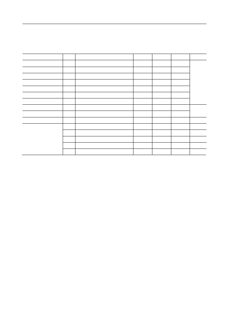
Secondary Function
Function
Pin
Type
Description
Secondary function of P0.0:
Input pin for external interrupt 0. This pin can
receive an input at the rising edge, falling edge, or
both the rising/falling edges.
External
Interrupt
Control
I
8
Secondary function of P0.4:
Input pin for external interrupt 1. This pin can
receive input at the rising edge, falling edge or both
the rising/falling edges. Also used as a gate signal
input pin to enable or disable the count of timer 0.
I
4
Secondary function of P0.1:
Hardware stop mode input pin. When this pin is
set to the "L" level while the HSTP bit in SBYCON
is set to "1", the hardware stop mode is entered.
In the hardware stop mode, oscillation on the OSC
side is stopped for low power consumption.
I
7
5
Secondary function of P0.3:
External clock input pin for timer 0.
I
Timer 0
6
Secondary function of P0.2:
Output pin that provides waveform with twice the
cycle of the overflow of timer 1.
O
Timer 1
Secondary function of P3.0 to 3.7:
These are used for analog channels during A/D
conversion.
I
A/D Converter
16
23
to
3
Secondary function of P0.5:
Output pin that provides clocks equal to OSCCLK
divided by 2 or 4, and also clocks equal to XTCLK
divided by 2 or 4.
O
Clock Output
59
Secondary function of P1.4:
Input pin for remote control.
I
Remote Control
Input
56
Secondary function of P1.7:
Data output pin for shift register 1.
O
57
Secondary function of P1.6:
Data input pin for shift register 1.
I
58
Secondary function of P1.5:
Sync clock I/O pin for shift register 1.
This provides clock output when used as the
master, while it functions as clock input when
used as a slave.
I/O
Shift Register
Symbol
INT0
INT1
HSTOP
T0CK
T1OUT
AI7
AI0
to
CLKOUT
RMCIN
SFTO1
SFTI1
SFTCK1
8/15
° Semiconductor
MSM65352/65352B
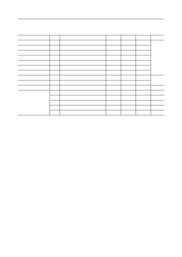
ABSOLUTE MAXIMUM RATINGS
Parameter
Symbol
Condition
Rating
Unit
Supply Voltage
V
DD
≠0.3 to 7.0
Input Voltage
V
I
≠0.3 to V
DD
+0.3
Output Voltage
V
O
≠0.3 to V
DD
+0.3
Power Dissipation
P
D
400
Ta = 25∞C
Ta = 25∞C, per package
50
Ta = 25∞C, per output
Storage Temperature
T
STG
--
≠55 to +150
V
mW
∞C
RECOMMENDED OPERATING CONDITIONS
Parameter
Symbol
Condition
Range
Unit
Supply Voltage
V
DD
2.7 to 5.5
Memory Hold Voltage
V
DDMH
2.0 to 5.5
f
OSC
1 to 10
Oscillation Frequency*
1
f
XT
32.768
f
OSC
= 0Hz
V
DD
= 2.7 to 5.5
0 to 10
--
Operating Temparature
T
op
--
≠20 to +70
V
MHz
∞C
--
--
f
EXTCLK
External Clock
Operating Frequency*
2
kHz
MHz
*1 Determined by the crystal oscillator or ceramic resonator to be used.
*2 External clock cannot be used in the XT pin.
9/15
° Semiconductor
MSM65352/65352B
ELECTRICAL CHARACTERISTICS
DC Characteristics 1 (V
DD
=4.5 to 5.5V)
Parameter
Symbol
Condition
Typ.
Unit
"H" Input Voltage 1
V
IH1
--
"H" Input Voltage 2
V
IH2
--
V
IL
--
"L" Input Voltage
V
OH1
--
CPUCLK=1MHz
I
OH
=
≠
200mA
--
I
OH
=
≠
400mA
"L" Output Voltage 1
V
OL1
I
OL
= 1.6mA
--
CPUCLK=1MHz
CPUCLK=1MHz
V
OH2
"H" Output Voltage 2
*1
*2
"H" Output Voltage 1
*3
*4
"L" Output Voltage 2
*3
*4
V
OL2
Input Leakage Current
*5
"L" Input Current
*6
I
LI2
I
IL
Input Capacitance
C
I
I
DD1
I
DD2
I
DD3
I
DD4
I
DD5
Operating Current
Consumption
V
DD
= 5V
XT = 32kHz
OSC = 10MHz
I
OL
= 3.2mA
V
I
= V
DD
/0V
V
I
= 0V, V
DD
= 5V
f = 1MHz, Ta = 25∞C
Stop mode
*7
CPUCLK = 32kHz, HALT mode
*8
CPUCLK = 32kHz, no load.
*9
CPUCLK = 10MHz, HALT mode
*7
CPUCLK = 10MHz, no load.
Min.
Max.
2.4
0.7V
DD
--
0.75V
DD
0.75V
DD
--
--
--
0.8
--
--
0.4
--
--
0.4
--
--
±10
≠
200
≠
40
≠
400
5
--
--
15
--
30
30
--
60
80
--
160
8
--
16
20
--
40
mA
mA
mA
mA
mA
pF
mA
V
(GND = 0V, Ta = ≠20 to +70∞C)
*1 Excluding OSC0 and RESET
*2 Only for OSC0 and RESET
*3 Excluding P4
*4 Only for P4
*5 Excluding RESET
*6 Only for RESET
*7 Measured when LCD is operated
*8 Measured when OSC clock is stopped but LCD is operated without load
*9 Measured when OSC clock is stopped
10/15
° Semiconductor
MSM65352/65352B
DC Characteristics 2 (2.7V
£V
DD
<4.5V)
Parameter
Symbol
Condition
Typ.
Unit
"H" Input Voltage 1
V
IH1
--
"H" Input Voltage 2
V
IH2
--
V
IL
--
"L" Input Voltage
V
OH1
--
CPUCLK=1MHz
I
OH
=
≠
10mA
--
I
OH
=
≠
20mA
"L" Output Voltage 1
V
OL1
I
OL
= 10mA
--
CPUCLK=1MHz
CPUCLK=1MHz
V
OH2
"H" Output Voltage 2
*1
*2
"H" Output Voltage 1
*3
*4
"L" Output Voltage 2
*3
*4
V
OL2
Input Leakage Current
*5
"L" Input Current
*6
I
LI2
I
IL
Input Capacity
C
I
I
DD1
I
DD2
I
DD3
I
DD4
I
DD5
Operating Current
Consumption
V
DD
= 3V
XT = 32KHz
OSC = 5MHz
I
OL
= 20mA
V
I
= V
DD
/0V
V
I
= 0V, V
DD
= 3V
f = 1MHz, Ta = 25∞C
Stop mode
*7
CPUCLK = 32kHz, HALT mode
*8
CPUCLK = 32kHz, no load.
*9
CPUCLK = 5MHz, HALT mode
*7
CPUCLK = 5MHz, no load.
Min.
Max.
0.3V
DD
+0.9
0.6V
DD
+0.6
--
0.75V
DD
0.75V
DD
--
--
--
0.3V
DD
≠0.1
--
--
0.1
--
--
0.1
--
--
±10
≠
125
≠
40
≠
250
5
--
--
4
--
8
15
--
30
45
--
90
1.5
--
3
5
--
14
mA
mA
mA
mA
mA
pF
mA
V
(GND = 0V, Ta =
≠
20 to +70∞C)
*10
*11
*1 Excluding OSC0 and RESET
*2 Only for OSC0 and RESET
*3 Excluding P4
*4 Only for P4
*5 Excluding RESET
*6 Only for RESET
*7 Measured when LCD is operated
*8 Measured when OSC clock is stopped but LCD is operated without load
*9 Measured when OSC clock is stopped
*10 More than 3.375V
*11 Less than 0.8V

11/15
° Semiconductor
MSM65352/65352B
A/D Converter Characteristics 1
Symbol
Condition
Min.
Typ.
Max.
Unit
AINFH
(ADOUT)=F
H
4.77
5.00
--
AINEH
(ADOUT)=E
H
4.45
4.53
4.61
AINDH
(ADOUT)=D
H
4.14
4.22
4.30
AINCH
(ADOUT)=C
H
3.83
3.91
3.98
AINBH
(ADOUT)=B
H
3.52
3.59
3.67
AINAH
(ADOUT)=A
H
3.20
3.28
3.36
AIN9H
(ADOUT)=9
H
2.89
2.97
3.05
AIN8H
(ADOUT)=8
H
2.58
2.66
2.73
AIN7H
(ADOUT)=7
H
2.27
2.34
2.42
AIN6H
(ADOUT)=6
H
1.95
2.03
2.11
AIN5H
(ADOUT)=5
H
1.64
1.72
1.80
AIN4H
(ADOUT)=4
H
1.33
1.41
1.48
AIN3H
(ADOUT)=3
H
1.02
1.09
1.17
AIN2H
(ADOUT)=2
H
0.70
0.78
0.86
AIN1H
(ADOUT)=1
H
0.39
0.47
0.55
AIN0H
(ADOUT)=0
H
--
0.00
0.23
t
SET
--
--
60
200
ms
Parameter
A/D Conversion
Analog Input
Detecting Voltage
A/D Conversion
Settling Time
V
(V
DD
=A
VDD
=5V, GND=AGND=0V, Ta=≠20 to +70∞C)
12/15
° Semiconductor
MSM65352/65352B
A/D Converter Characteristics 2
Symbol
Condition
Min.
Typ.
Max.
Unit
AINFH
(ADOUT)=F
H
2.88
3.00
--
AINEH
(ADOUT)=E
H
2.69
2.72
2.75
AINDH
(ADOUT)=D
H
2.50
2.53
2.56
AINCH
(ADOUT)=C
H
2.32
2.34
2.37
AINBH
(ADOUT)=B
H
2.13
2.16
2.18
AINAH
(ADOUT)=A
H
1.94
1.97
2.00
AIN9H
(ADOUT)=9
H
1.75
1.78
1.81
AIN8H
(ADOUT)=8
H
1.57
1.59
1.62
AIN7H
(ADOUT)=7
H
1.38
1.41
1.43
AIN6H
(ADOUT)=6
H
1.19
1.22
1.25
AIN5H
(ADOUT)=5
H
1.00
1.03
1.06
AIN4H
(ADOUT)=4
H
0.82
0.89
0.87
AIN3H
(ADOUT)=3
H
0.63
0.66
0.68
AIN2H
(ADOUT)=2
H
0.44
0.47
0.50
AIN1H
(ADOUT)=1
H
0.25
0.28
0.31
AIN0H
(ADOUT)=0
H
--
0.00
0.12
t
SET
--
--
60
200
ms
Parameter
A/D Conversion
Analog Input
Detecting Voltage
A/D Conversion
Settling Time
V
(V
DD
=A
VDD
=3V, GND=AGND=0V, Ta=≠20 to +70∞C)
13/15
° Semiconductor
MSM65352/65352B
AC Characteristics
∑ CPU control
∑ Peripheral control 1
Parameter
Symbol
Condition
Unit
t
C
V
DD
= 4.5 to 5.5V
Min.
Max.
--
(V
DD
= 2.7 to 5.5V, GND = 0V, Ta = ≠20 to +70∞C)
100
ns
OSC
Clock Cycle
--
0.55 t
C
0.45 t
C
EXI
External Interrupt
Pulse Width
t
EXIW
--
4 t
C
--
2.7V £ V
DD
< 4.5V
--
200
t
CLW
Clock "L" Pulse Width
RESET Pulse Width
t
RESW
(V
DD
= 2.7 to 5.5V, GND = 0V, Ta = ≠20 to +70∞C)
ns
Parameter
Symbol
Condition
Unit
--
Min.
Max.
--
20
∑ Peripheral control 2
See Timing Diagram.
Parameter
Symbol
Condition
Unit
t
C
V
DD
= 4.5 to 5.5V
Min.
Max.
--
(V
DD
= 2.7 to 5.5V, GND = 0V, Ta = ≠20 to +70∞C)
100
ns
OSC
Clock Cycle
2.7V £ V
DD
< 4.5V
--
200
SFTCK1 Cycle
t
SFC
SFT1
SFTCK1 "L" Pulse Width
t
SFCLW
SFTCK1 "H" Pulse Width
t
SFCHW
C
L
= 100 pF
--
--
--
8 t
C
4 t
C
≠20
4 t
C
≠20
SFTO1 Setup Time
t
SFOS
SFTO1 Hold Time
t
SFOH
SFTI1 Setup Time
t
SFIS
SFTI 1Hold Time
t
SFIH
--
--
t
SFCLW≠100
t
SFCHW≠100
--
--
100
100

14/15
° Semiconductor
MSM65352/65352B
Timing Diagram
∑ CPU control
RESET
t
RESW
1) RESET pulse width
∑ Peripheral control 1
OSC0
t
C
t
CLW
INT0 - 2
t
EXIW
1) EXI pulse width
∑ Peripheral control 2
SFTO1
SFTI1
t
SFIS
1) SFT1
SFTCK
t
SFIH
t
SFOS
t
SFOH
t
SFCLW
t
SFCHW
t
SFC
15/15
° Semiconductor
MSM65352/65352B
(Unit : mm)
PACKAGE DIMENSIONS
Notes for Mounting the Surface Mount Type Package
The SOP, QFP, TSOP, SOJ, QFJ (PLCC), SHP and BGA are surface mount type packages, which
are very susceptible to heat in reflow mounting and humidity absorbed in storage.
Therefore, before you perform reflow mounting, contact Oki's responsible sales person for the
product name, package name, pin number, package code and desired mounting conditions
(reflow method, temperature and times).
QFP64-P-1414-0.80-BK
Package material
Lead frame material
Pin treatment
Solder plate thickness
Package weight (g)
Epoxy resin
42 alloy
Solder plating
5 mm or more
0.87 TYP.
Mirror finish