
° Semiconductor
MSM6542-01/02/03
68
DESCRIPTION
The MSM6542 is a perpetual-calendar-based
real time clock with an alarm function which
can read and write data in units of seconds. It
can be connected to various buses and can
function as a peripheral IC of a microcom-
puter.
The clock ranges are seconds, minutes, hours,
days, months, years, and days of the week.
The alarm ranges are seconds, minutes, hours,
days, months, and days of the week.
An event trigger is generated when the time
matches the specified time and an alarm oc-
curs or when the clock counter generates a
carry. The interrupt and pulse outputs are
provided for each of an alarm and a carry.
An interface with a microcomputer is imple-
mented by four data bus pins, four address
bus
° Semiconductor
MSM6542-01/02/03
REAL TIME CLOCK WITH PERIODIC AND ALARM OUTPUT
bus pins, three control bus pins, and two chip
select pins. These pins are used to write or
read data from the clock, alarm, and control
registers, or to modify the data.
The MSM6542 has an address latch enable
(ALE) input pin, allowing the data bus and
address bus to be shared. When the ALE
input pin is kept high, the data bus and ad-
dress bus can be exclusively used.
Other functions of the MSM6542 are: a 30-
second adjustment, stop and restart of clock,
data registers as RAM, and data register (RAM)
protection.
The CMOS circuitry used in the MSM6542
affords low power dissipation. The crystal
oscillator operates at 32.768 kHz. Provisions
for backup time keeping are included.
FEATURES
∑ Real time clock providing seconds, minutes,
hours, days, months, years, and days of
the week.
∑ Multiple alarm ranges covering seconds,
minutes, hours, days, months, and days of
the week. A desired alarm range can be
selected.
∑ A periodic interrupt output interval can
be selected over a wide range from 1/1024
seconds up to 10 minutes.
∑ Interface flexibility allows for connection
to many types of microprocessors.
∑ Single read-out procedure (Read flag).
∑ Single power sense circuitry. (Data protect
function).
∑ Unused registers can be used as RAM.
∑ 30-second adjustment by software or
hardware (software only for the MSM6542-
1/-2).
∑ Stop and restart of clock by software or
hardware (software only for the MSM6542-
1/-2).
∑ 1 Hz output for adjustment and check of
oscillation frequency (MSM6542-3 only).
∑ User selection of 12 or 24 hour clock mode.
∑ Address latch enable (ALE) input pin.
∑ Advanced CMOS circuitry allows low
stand-by voltage and current.
∑ User standard 32.768 kHz oscillator crys-
tal
∑ Available in multiple packages
18-pin plastic DIP (for the MSM6542-
1RS/2RS) (DIP18-P-300).
20-pin plastic SOP (for the MSM6542-
1MS-K/2MS-K) (SSOP20-P-250-K).
24-pin plastic DIP (for the MSM6542-
3RS) (DIP24-P-600).
24-pin plastic SOP (for the MSM6542-
3GS-VK) (SOP24-P-430-VK).
∑ Pin assignment compatibility with the
MSM6242BRS (The MSM6542-3MSK pro-
vides near compatibility.).
° Semiconductor
MSM6542-01/02/03
69
INTERRUPT
OUT
1
2
3
4
5
6
7
8
9
18
17
16
14
13
12
11
10
ALE
15
E
V
SS
XT
XT
R/W
A
1
A
0
A
2
A
3
D
0
D
1
D
2
D
3
CS
1
CS
0
V
DO
INTERRUPT
OUT
1
2
3
4
5
6
7
8
9
18
17
16
14
13
12
11
10
ALE
15
RD
V
SS
XT
XT
WR
A
1
A
0
A
2
A
3
D
0
D
1
D
2
D
3
CS
1
CS
0
V
DO
1
24
2
23
3
22
4
21
5
20
6
7
18
8
17
9
16
10
15
11
14
12
13
19
PERIODIC
OUT
ALARM OUT
ALE
30Sec. ADJ
68/80
(E) RD
V
SS
XT
XT
(NC)
STOP/START
1Hz
WR (R/W)
CS
0
A
0
A
1
A
2
A
3
D
1
D
2
D
3
CS
1
1
2
19
3
20
18
4
17
5
16
6
15
7
14
8
13
9
12
10
11
INTERRUPT OUT
(NC)
ALE
A
0
CS
0
A
1
A
2
A
3
RD
V
SS
XT
XT
(NC)
WR
CS
1
D
0
D
1
D
2
D
3
V
DO
1
2
19
3
20
18
4
17
5
16
6
15
7
14
8
13
9
12
10
11
INTERRUPT OUT
(NC)
ALE
A
0
CS
0
A
1
A
2
A
3
E
V
SS
XT
XT
(NC)
R/
W
CS
1
D
0
D
1
D
2
D
3
V
DO
12
13
11
14
10
15
9
16
8
17
7
18
6
19
5
20
4
21
3
22
2
23
1
24
PERIODIC OUT
ALARM OUT
ALE
CS
0
A
0
A
1
30Sec. ADJ
A
2
A
3
68/80
(E) RD
V
SS
XT
XT
(NC)
STOP/START
1Hz
CS
1
D
0
D
1
D
2
D
3
WR (R/W)
V
DO
V
DO
D
0
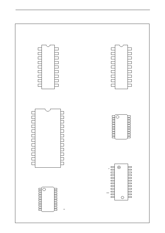
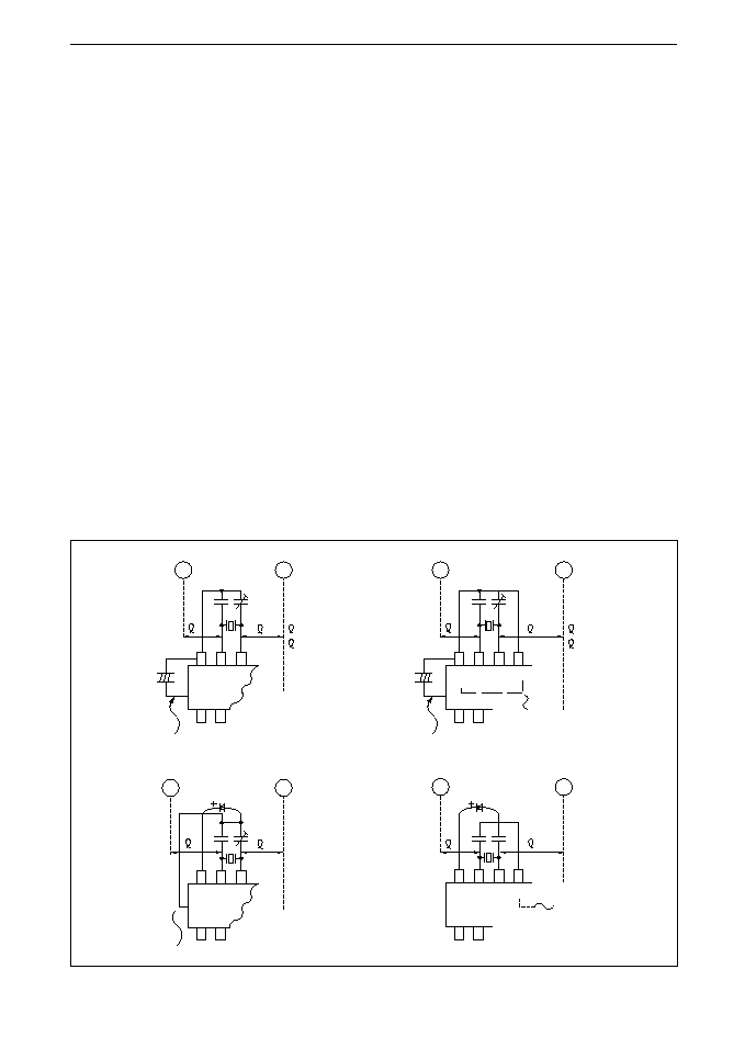
PIN CONFIGURATION
MSM6542-01RS
18-pin plastic DIP (top view)
MSM6542-02RS
18-pin plastic DIP (top view)
MSM6542-03RS
24-pin plastic DIP (top view)
MSM6542-01MS-K
20-pin plastic SOP (top view)
MSM6542-02MS-K
20-pin plastic SOP (top view)
MSM6542-03GS-VK
24-pin plastic SOP (top view)
NC : NO Connected (open)
° Semiconductor
MSM6542-01/02/03
70
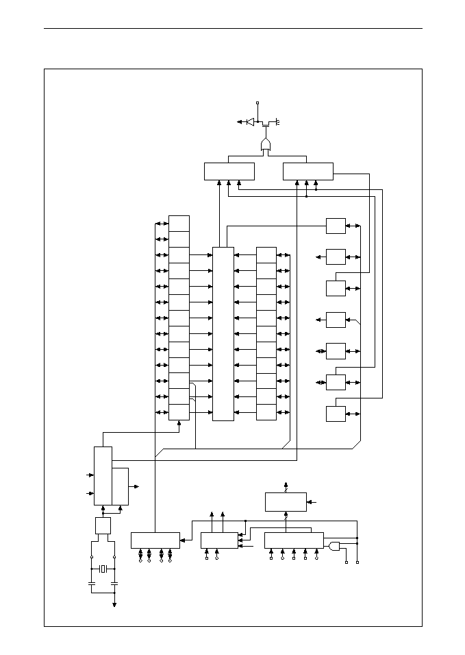
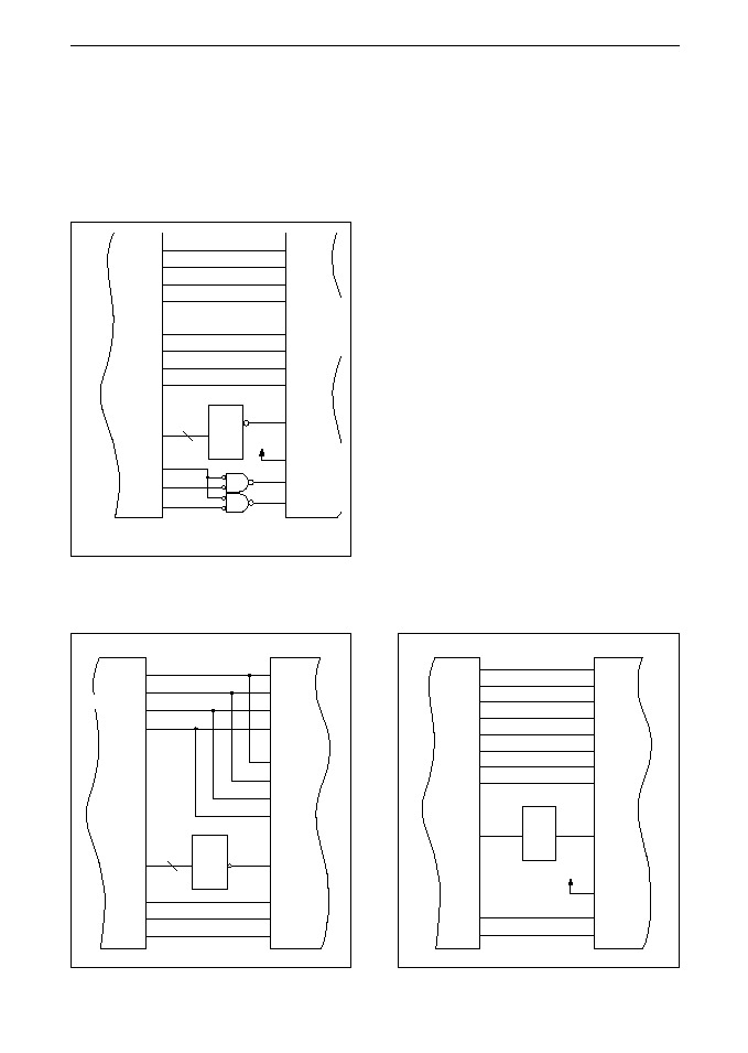
FUNCTIONAL BLOCK DIAGRAM (MSM6542-01, 02)
32.768KHz
XT
XT
OSC
RESET
STOP
Less-than-second
counter
Control
counter
D
A
T
A
I.
F.
D
3
D
2
D
1
D
0
A
3
A
2
A
1
A
0
CS
0
WR
or R/
W
RD
or E
(-1) (-2)
R/W
I
F
D.P.
A D D R E S S
I.
F.
D E C O D E R
BANK 1/0
ALE
CS
1
R-S
I
to C
F
A-S
I
to C
E'
R-S
1
R-S
10
R-
MI
10
R-H
1
R-H
10
R-W
R-D
1
R-D
10
R-
MO
1
R-
MO
10
R-Y
1
R-Y
10
COMPARATOR
A-S
1
A-S
10
A-H
1
A-H
10
A-W
A-D
1
A-D
10
A- MO
1
A- MO
10
A- MI
10
INTERRUPT OUT
C
E'
C
C'
A-EN ABLE
C
D'
C
F
C
E
C
D
R-
MI
1
A- MI
1
A L A R M
O U T
P E R I O D I C
O U T
° Semiconductor
MSM6542-01/02/03
71
32.768KHz
XT
XT
OSC
RESET
STOP
1Hz
Less-than-second
counter
Control
counter
D
A
T
A
I.
F.
R/W
I
F
D.P.
A D D R E S S
I.
F.
D E C O D E R
BANK 1/0
D
3
D
2
D
1
D
0
A
3
A
2
A
1
A
0
CS
0
R/
W
or
WR
E or
RD
68/80
ALE
CS
1
30sec. ADJ
STOP/START
R-S
I
to C
F
A-S
I
to C
E'
R-S
1
R-S
10
R- MI
10
R-H
1
R-H
10
R-W
R-D
1
R-D
10
R- MO
1
R- MO
10
R-Y
1
R-Y
10
COMPARATOR
A-S
1
A-S
10
A-H
1
A-H
10
A-W
A-D
1
A-D
10
A- MO
1
A- MO
10
A- MI
10
P E R I O D I C
O U T
C
E'
C
C'
A-EN ABLE
C
D'
C
F
C
E
C
D
ALARM OUT
PERIODIC OUT
R- MI
1
A- MI
1
A L A R M
O U T
FUNCTIONAL BLOCK DIAGRAM (MSM6542-03)
° Semiconductor
MSM6542-01/02/03
72
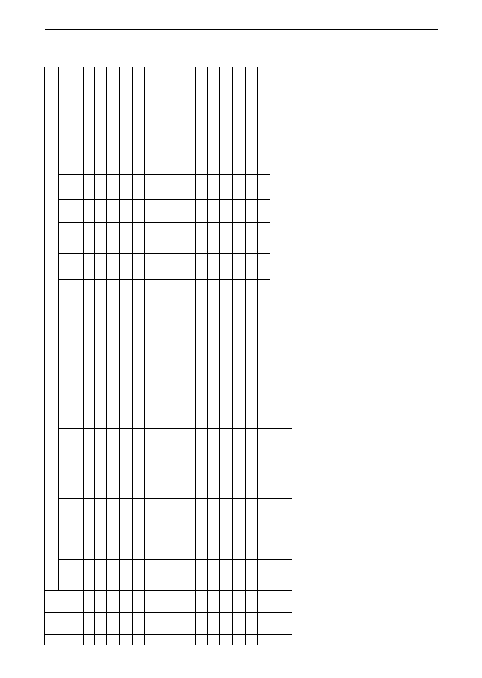
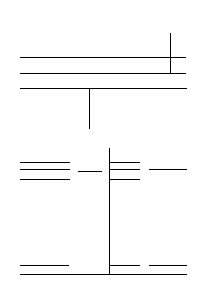
REGISTER TABLE
A
d
d
r
e
s
s
A
3
A
2
A
1
A
0
Register
symbol
D
3
D
2
D
1
D
0
Register name
BANK 0
BANK 1
0
1
2
3
4
5
6
7
8
9
A
B
C
D
E
F
0
0
0
0
0
0
0
0
1
1
1
1
1
1
1
1
0
0
0
0
1
1
1
1
0
0
0
0
1
1
1
1
0
0
1
1
0
0
1
1
0
0
1
1
0
0
1
1
0
1
0
1
0
1
0
1
0
1
0
1
0
1
0
1
R-S
1
R-S
10
R-MI
1
R-MI
10
R-H
1
R-H
10
R-D
1
R-D
10
R-MO
1
R-MO
10
R-Y
1
R-Y
10
R-W
C
D
C
E
C
F
r-s
8
≠
r-mi
8
≠
r-h
8
≠
r-d
8
*
r-mo
8
*
r-y
8
r-y
80
≠
IT/PLS
2
IRQ FLAG
0
BANKI/0
r-s
4
r-s
40
r-mi
4
r-mi
40
r-h
4
r-pm/am
r-d
4
*
r-mo
4
*
r-y
4
r-y
40
r-w
4
IT/PLS
1
REST
STOP
r-s
2
r-s
20
r-mi
2
r-mi
20
r-h
2
r-h
20
r-d
2
r-d
20
r-mo
2
*
r-y
2
r-y
20
r-w
2
MASK
2
IRQ FLAG
2
30-s
adjustment
r-s
1
r-s
10
r-mi
1
r-mi
10
r-h
1
r-h
10
r-d
1
r-d
10
r-mo
1
r-mo
10
r-y
1
r-y
10
r-w
1
MASK
1
IRQ FLAG
1
READ FLAG
Real time one-second digit register
Real time ten-second digit register
Real time one-minute digit register
Real time ten-minute digit register
Real time one-hour digit register
Real time PM/AM ten-hour digit register
Real time one-day digit register
Real time ten-day digit register
Real time one-month digit register
Real time ten-month digit register
Real time one-year digit register
Real time ten-year digit register
Real time day-of-week register
Control D register
Control E register
Control F register
Register
symbol
A-S
1
A-S
10
A-MI
1
A-MI
10
A-H
1
A-H
10
A-D
1
A-D
10
A-MO
1
A-MO
10
A-W
A-ENABLE
C
C'
C
D'
C
E'
D
3
a-s
8
*
a-mi
8
*
a-h
8
*
a-d
8
*
a-mo
8
*
*
a-e
8
≠
≠
HD/SFT
D
2
a-s
4
a-s
40
a-mi
4
a-mi
40
a-h
4
a-PM/AM
a-d
4
*
a-mo
4
*
a-w
4
a-e
4
≠
CY
2
24/12
D
1
a-s
2
a-s
20
a-mi
2
a-mi
20
r-h
2
a-h
20
a-d
2
a-d
20
a-mo
2
*
a-w
2
a-e
2
TEST
2
CY
1
CAL
D
0
a-s
1
a-s
10
a-mi
1
a-mi
10
a-h
1
a-h
10
a-d
1
a-d
10
a-mo
1
a-mo
10
a-w
1
a-e
1
TEST
1
CY
0
DP
Register name
Alarm one-second digit register
Alarm ten-second digit register
Alarm one-minute digit register
Alarm ten-minute digit register
Alarm one-hour digit register
Alarm PM/AM ten-hour digit register
Alarm one-day digit register
Alarm ten-day digit register
Alarm one-month digit register
Alarm ten-month digit register
Alarm day-of-week register
Register to specify the alarm range
Control C register
Control D' register
Control E' register
Same as BANK 0
Since positive logic is used, the high level on a data bus corresponds to 1 in a register.
When DP = 1, data can be written in the BANK 1/0 and DP bits.
Wnen 0 is written in the DP bit, a delay is required until the bit is set at 0.
READ FLAG and IRQ.FLAG
0
are read-only flags. READ FLAG is cleared after data is read from it.
IRQ. FLAG
1
is cleared after data is read from it with IT/PLS
1
set at 1. When IT/PLS
1
is 0, only 0 can be written in IRQ. FLAG
1
and it cannot be cleared when it is read. Similarly, IRQ. FLAG
2
is cleared after
data is read from it with IT/PLS
2
set at 1. When IT/PLS
2
is 0, only 0 can be written in IRQ. FLAG
2
and it cannot be cleared when it is read.
For the MSM6542-01/02, HD/SFT is set internally at 0.
Data can be written in the C
C'
register but it is cleared when it is read. Therefore, read data is always 0.
When r-pm/am is 1, the time is P.M. When it is 0, the time is A.M. This is also true for a-pm/am.
The contents of all registers are unpredictable when power is turned on from 0V to 5V.
A hyphen in the table indicates that the bit is not present. When the bit is read, it always provides 0.
When a bit marked an asterisk (*) in the table is used as part of a clock register or alarm register, it always provides 0 at r
ead. When the bit is used as part of RAM, however, it can be used for read and
write.
1.
2.
3.
4.
5.
6.
7.
8.
9.
10.
11.
Notes:
° Semiconductor
MSM6542-01/02/03
73
Rating
Symbol
Condition
Value
Unit
Power supply voltage
V
DD
Ta = 25įC
≠0.3 to 7
V
Input voltage
V
I
Ta = 25įC
≠0.3 to V
DD
+0.3
V
Output voltage
V
O
Ta = 25įC
≠0.3 to V
DD
+0.3
V
Storage temperature range
T
STG
≠
≠55 to +150
įC
Absolute Maximum Ratings
ELECTRICAL CHARACTERISTICS
Rating
Symbol
Condition
Value
Unit
Power supply voltage
V
DD
≠
4.5 to 5.5
V
Clock power supply voltage
V
CLK
≠
2.0 to 6
V
Crystal oscillator frequency
(xt)
≠
32.768
kHz
Operating temperature range
T
OP
≠
≠40 to +85
įC
Operation Range
Note:
The clock power supply voltage is required to assure operation of the crystal oscillator and clock.
Rating
Symbol
Condition
Max.
Applicable pin
DC Characteristics
Typ.
Min.
High input voltage (1)
Low input voltage (2)
Input leakage (1)
Input leakage (2)
High input current
Low input current
High output voltage
Low output voltage (1)
Low output voltage (2)
Leakage current
Current consumption (1)
Current consumption (2)
Input capacitance (1)
Input capacitance (2)
High input voltage (2)
V
IH1
V
IL2
I
LK1
I
LK2
I
IH
I
IL
V
OH
V
OL1
V
OL2
I
OFFLK
I
DD1
I
DD2
C
I1
C
I2
V
IH2
V
1
= V
DD
/0V
V
IH
= 0.8 V
DD
V
IL
= 0.2 V
DD
I
OH
= ≠400 ĶA
I
OL
= 2.5 mA
I
OL
= 2.5 mA
V
I
= V
DD
/0V
Oscillation at 32.768 kHz
V
DD
= 5V
CS
1
0V V
DD
= 2V
Input oscillator
Frequency 1 MHz
2.2
≠
≠1
≠10
≠100
20
2.4
≠
≠
≠
≠
≠
≠
≠
≠
≠
≠
≠
≠
≠
≠
≠
≠
≠
≠
≠
3
5
≠
≠
0.2
V
DD
1
10
≠20
100
≠
0.4
0.4
10
30
5
≠
≠
≠
V
ĶA
pF
V
ĶA
ĶA
Low input voltage (1)
V
IL1
0.8
V
DD
≠
≠
0.8
CS
0
, A
0
~A
3
, D
0
~ D
3
RD (E), WR (R/W),
ALE, 30-s ADJ
STOP/START
CS
1
, 68/80
CS
0
, ALE, A
0
~ A
3
,
68/80, RD (E), WR
(R/W), CS1, 30-s ADJ
D
0
~ D
3
, STOP/START
STOP/START
D
0
~ D
3
, 1Hz
INTERRUPT
PERIODIC OUT
ALARM
V
DD
Input pins other than
D
O
to D
3
D
0
to D
3
(V
DD =
5V Ī10%, Ta = -40 ~ +85įC)
~
~
° Semiconductor
MSM6542-01/02/03
74
CS
1
A
0
~ A
3
CS
0
WR
D
0
~ D
3
(Input)
V
IH2
t
C1S
t
C1H
V
IH1
V
IL1
t
RCV
t
AW
t
DH
V
IH1
V
IL1
V
IHI
= 2.2V
V
IL1
= 0.8V
5
4
1
5
V
IH2
= V
DD
V
IL2
= V
DD
V
IH2
V
IH1
V
IL1
V
IL1
V
IH1
V
IH1
V
IH1
V
IL1
t
WW
t
WA
V
IH1
V
IL1
t
DS
Rating
Symbol
Condition
Max.
Unit
≠
≠
≠
≠
≠
≠
≠
≠
(V
DD
= 5V Ī10%, Ta = ≠40 to +85įC (in the 80 mode for the MSM6542-01/03))
80-xxx
Write mode (ALE is always at V
DD
.)
≠
≠
≠
≠
≠
≠
≠
≠
Typ.
1000
1000
20
10
120
100
10
100
Min.
t
C1S
t
C1H
t
AW
t
WA
t
WW
t
DS
t
DH
t
RCV
Switching Characteristics
CS
1
set-up time
CS
1
hold time
Address stable before WRITE
Address stabel after WRITE
WRITE pulse width
Data set-up time
Data hold time
RD/WR recovery time
ns
ns
ns
ns
ns
ns
ns
ns
≠
≠
≠
≠
≠
≠
≠
≠

° Semiconductor
MSM6542-01/02/03
75
CS
1
A
0
~ A
3
CS
0
D
0
~ D
3
(Output)
V
IH2
t
C1S
t
C1H
V
IH1
V
IL1
t
RCV
t
DR
V
OH
V
OL
V
IH1
= 2.2V
V
IL1
= 0.8V
5
4
1
5
V
IH2
= V
DD
V
IL2
= V
DD
V
IH2
V
IH1
V
IL1
V
IL1
V
IH1
V
IH1
V
OH
V
OL
t
RA
t
RD
t
AR
"Z"
V
OH
= 2.2V
V
OL
= 0.8V
RD
Rating
Symbol
Condition
Max.
Unit
≠
≠
≠
≠
CL = 150 pF
≠
≠
(V
DD
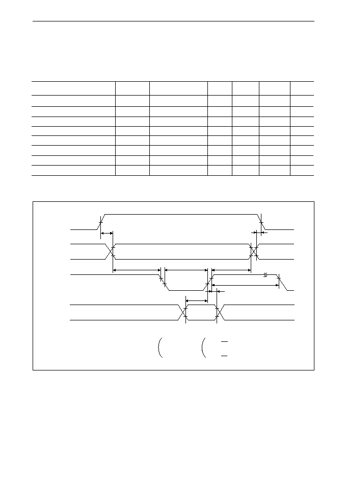
= 5V Ī10%, Ta = ≠40 to +85įC (in the 80 mode for the MSM6542-01/03))
80-xxx
Read mode (ALE is always at V
DD
.)
≠
≠
≠
≠
120
45
≠
Typ.
≠
≠
≠
≠
≠
≠
≠
Min.
1000
1000
20
20
≠
10
100
t
C1S
t
C1H
t
AR
t
RA
t
RD
t
DR
t
RCV
CS
1
set-up time
CS
1
hold time
Address stable before READ
Address stable after READ
RD to data
Data hold
RD/WR recovery time
ns
ns
ns
ns
ns
ns
ns
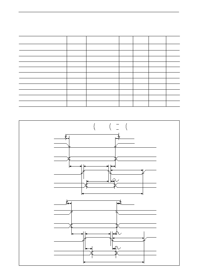
° Semiconductor
MSM6542-01/02/03
76
CS
1
A
0
~ A
3
CS
0
ALE
WR
D
0
~ D
3
(Input)
V
IH2
t
C1S
t
AS
t
AH
V
IH1
V
IL1
t
C1H
t
AW
t
ALW
t
WW
t
WAL
t
RCV
t
DS
t
DH
V
IH1
= 2.2V
V
IL1
= 0.8V
5
4
5
1
V
IH2
= V
DD
V
IL2
= V
DD
V
IH2
V
IH1
V
IL1
V
IH1
V
IH1
V
IL1
V
IH1
V
IL1
V
IH1
V
IL1
V
IH1
V
IH1
V
IL1
V
IH1
V
IL1
Rating
Symbol
Condition
Max.
Unit
≠
≠
≠
≠
≠
≠
≠
≠
≠
≠
≠
(V
DD
= 5V Ī10%, Ta = ≠40 to +85įC (in the 80 mode for the MSM6542-01/03))
80-xxx
Write mode (ALE is used.)
≠
≠
≠
≠
≠
≠
≠
≠
≠
≠
≠
Typ.
≠
≠
≠
≠
≠
≠
≠
≠
≠
≠
≠
Min.
1000
25
25
40
10
120
20
100
10
1000
100
t
C1S
t
AS
t
AH
t
AW
t
ALW
t
WW
t
WAL
t
DS
t
DH
t
C1H
t
RCV
CS
1
set-up time
Address set-up time
Address hold time
ALE pulse width
ALE before WRITE
WRITE pulse width
ALE after WRITE
Data set-up time
Data hold time
CS
1
hold time
RD/WR recovery time
ns
ns
ns
ns
ns
ns
ns
ns
ns
ns
ns
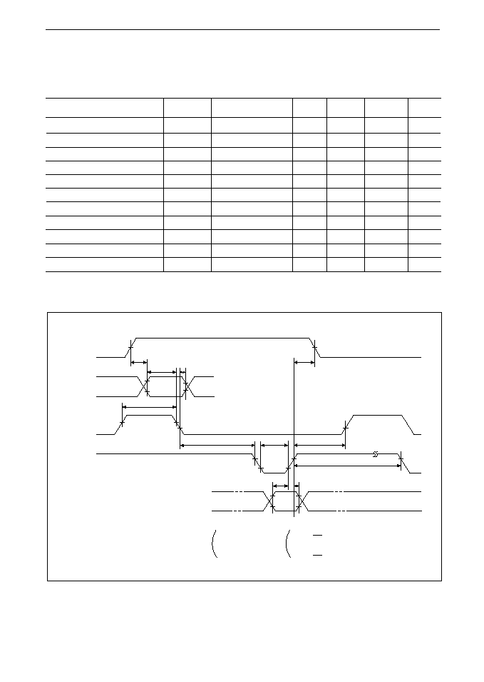
° Semiconductor
MSM6542-01/02/03
77
CS
1
A
0
~ A
3
CS
0
ALE
RD
D
0
~ D
3
(Output)
V
IH2
t
AH
t
AS
V
IH1
V
IL1
t
AW
t
RCV
t
ALR
t
RAL
t
RCV
t
RD
t
DR
V
OH
V
OL
V
IH1
= 2.2V
V
IL1
= 0.8V
5
4
5
1
t
C1S
V
IH2
= V
DD
V
IL2
= V
DD
V
OH
= 2.2V
V
OL
= 0.8V
V
IH2
V
IH1
V
IL1
t
C1H
V
IH1
V
IH1
V
IL1
V
IH1
V
IL1
V
IH1
V
IL1
V
IH1
V
IL1
"Z"
Rating
Symbol
Condition
Max.
Unit
≠
≠
≠
≠
≠
≠
CL = 150 pF
≠
≠
≠
(V
DD
= 5V Ī10%, Ta = ≠40 to +85įC (in the 80 mode for the MSM6542-01/03))
80-xxx
Read mode (ALE is used.)
≠
≠
≠
≠
≠
≠
120
45
≠
≠
Typ.
≠
≠
≠
≠
≠
≠
≠
≠
≠
≠
Min.
1000
25
25
40
10
20
≠
10
1000
100
t
C1S
t
AS
t
AH
t
AW
t
ALR
t
RAL
t
RD
t
DR
t
C1H
t
RCV
CS
1
set-up time
Address set-up time
Address hold time
ALE pulse width
ALE before READ
ALE after READ
RD to data
Data hold
CS
1
hold time
RD/WR recovery time
ns
ns
ns
ns
ns
ns
ns
ns
ns
ns
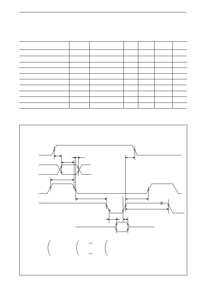
° Semiconductor
MSM6542-01/02/03
78
Rating
Symbol
Condition
Max.
Unit
≠
≠
≠
≠
≠
≠
≠
≠
CL = 150 pF
≠
≠
(V
DD
= 5V Ī10%, Ta = 0įC to +70įC (in the 86 mode for the MSM6542-02/03))
68-xxx
≠
≠
≠
≠
≠
≠
≠
≠
120
≠
≠
Typ.
≠
≠
≠
≠
≠
≠
≠
≠
≠
≠
≠
Min.
1000
100
220
20
220
500
180
20
≠
10
1000
t
C1S
t
RWE
t
EHW
t
ERW
t
ELW
t
EC
t
DS
t
DHW
t
RD
t
DHR
t
C1H
CS
1
set-up time
R/W address set-up time
E 'H' pulse width
R/W address hold time
E 'L' pulse width
E cycle time
Data set-up time
WRITE data hold time
E to data
READ data hold time
CS
1
hold time
ns
ns
ns
ns
ns
ns
ns
ns
ns
ns
ns
V
IH1
= 2.2V
V
IL1
= 0.8V
WRITE mode
CS
1
R/W
CS0
A
0
~ A
3
E
D
0
to D
3
V
IH2
t
C1S
t
C1H
V
IL1
V
IH1
t
RWE
t
EHW
t
ERW
t
ELW
t
DS
t
DHW
Input data
t
EC
READ mode
Output data
t
RD
V
OH
5
4
5
1
V
IH2
= V
DD
V
IL2
= V
DD
V
OH
= 2.2V
V
OL
= 0.8V
V
IH2
V
IL1
V
IL1
V
IH1
V
IL1
V
IL1
V
IH1
V
IH1
V
IL1
V
IL1
V
IH1
V
IL1
V
IH1
V
IL1
V
IH2
t
C1S
t
C1H
V
IH1
V
IL1
t
RWE
t
EHW
t
ERW
t
ELW
V
IH2
V
IH1
V
IH1
V
IL1
V
IH1
V
IL1
V
IH1
V
IH1
V
IL1
V
IL1
t
DHR
V
OL
V
OH
V
OL
t
EC
CS
1
R/W
CS0
A
0
~ A
3
E
D
0
to D
3

° Semiconductor
MSM6542-01/02/03
79
DESCRIPTION OF PINS
D
0
to D
3
(Data bus pins 0 to 3)
These input pins connected to the data bus of a microcomputer are used for the microcomputer
to read and write registers. The interface uses the positive logic. When CS
0
is low, CS
1
is high,
RD is low, and WR is high (for the 68-xxx system, CS
0
is low, CS
1
is high, R/W is high, and E is
high), these data bus pins are in the output mode. In the other cases, they are in the high
impedance status.
A
0
to A
3
(Address bus pins 0 to 3)
These input pins connected to the address bus of a microcomputer specify a register used by the
microcomputer for read or write. The address data specified by these pins is used in conjunction
with the input to the ALE pin.
ALE (Address Latch Enable)
This input pin is for address and CS
0
.
When the ALE pin is high, the address bus data and CS
0
are read into the IC. When it is low,
the address data and CS
0
read at ALE = H are retained in the IC. CS
1
functions independently
of the ALE pin.
When using an MSC-48-, MSC-51-, or 8085-based microcomputer having an ALE output pin,
connect this pin to the ALE output pin of the microcomputer. When a four-bit microcomputer
shares the four address bus pins, A
0
to A
3
, with another peripheral IC, the ALE pin on this IC
can be used to specify it.
When the microcomputer has no ALE output pin, connect the ALE input pin on this IC to the
V
DD
.
WR [R/W] (WRITE [READ/WRITE])
This input pin is connected to the WR pin for the 80-based CPU or the R/W pin for the 68-based
CPU.
RD [E] (READ [E])
This input pin is connected to the RD pin for the 80-based CPU or the E pin for the 68-based CPU.
CS
0
, CS
1
(Chip select pins 0 and 1)
These input pins enable or disable input of ALE, WR (R/W), and RD (E). When CS
0
is low and
CS
1
is high, these inputs are enabled. In the other combinations, the IC unconditionally assumes
that ALE is low and WR and RD are high (for the 68-based CPU, E is low). However, CS
0
needs
to operate in conjunction with ALE and CS
1
operates independently of ALE. Connect CS
1
to the
power supply voltage detection pin. For more information, see the descriptions in "USAGE"
and "USE OF CS
1
."
° Semiconductor
MSM6542-01/02/03
80
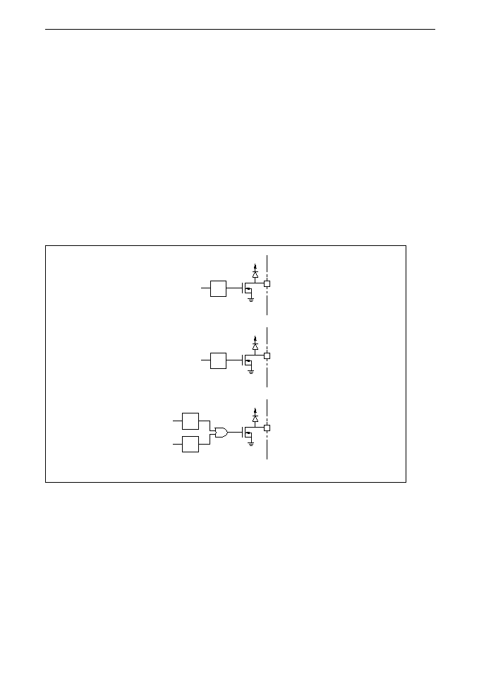
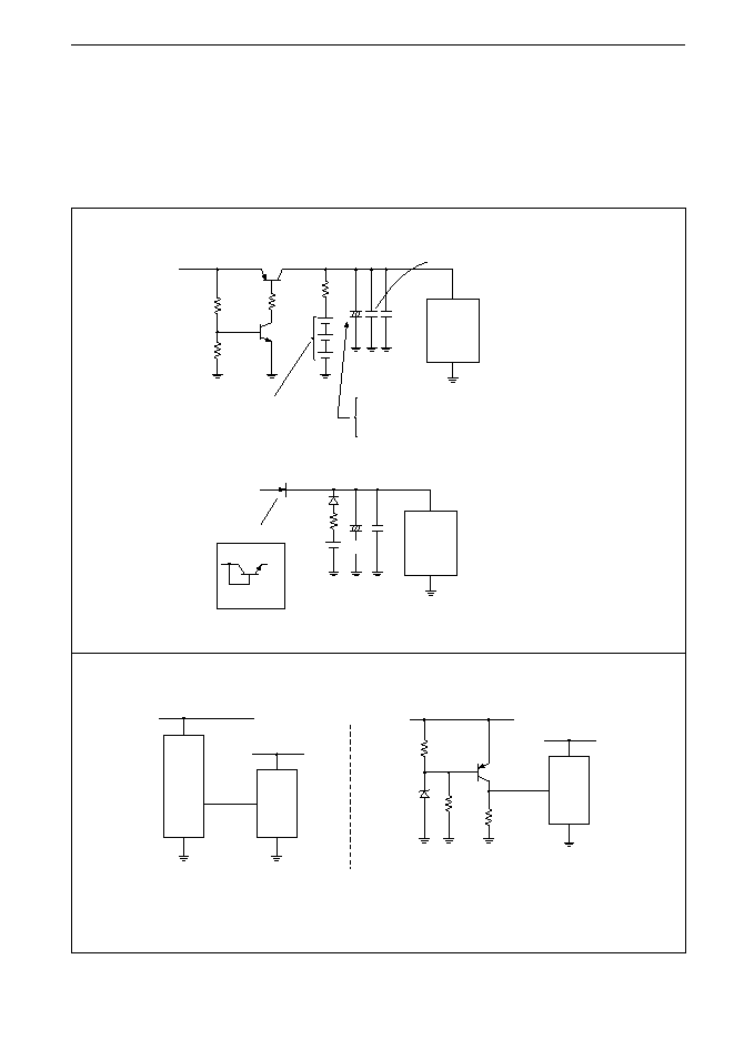
PERIODIC OUT (Only for the MSM6542-03)
This output pin is used for N-channel open drain. It outputs a single pulse or an
interrupt request as a trigger each time a carry is generated from the clock counter.
Output from this pin is not disabled by CS
0
and CS
1
.
ALARM OUT (Only for the MSM6542-03)
This output pin is used for N-channel open drain. It outputs a single pulse or an
interrupt request each time the contents of the clock counter match the date and time for
which an alarm is set. Output from this pin is not disabled by CS
0
and CS
1
.
INTERRUPT OUT (Only for the MSM6542-01/02)
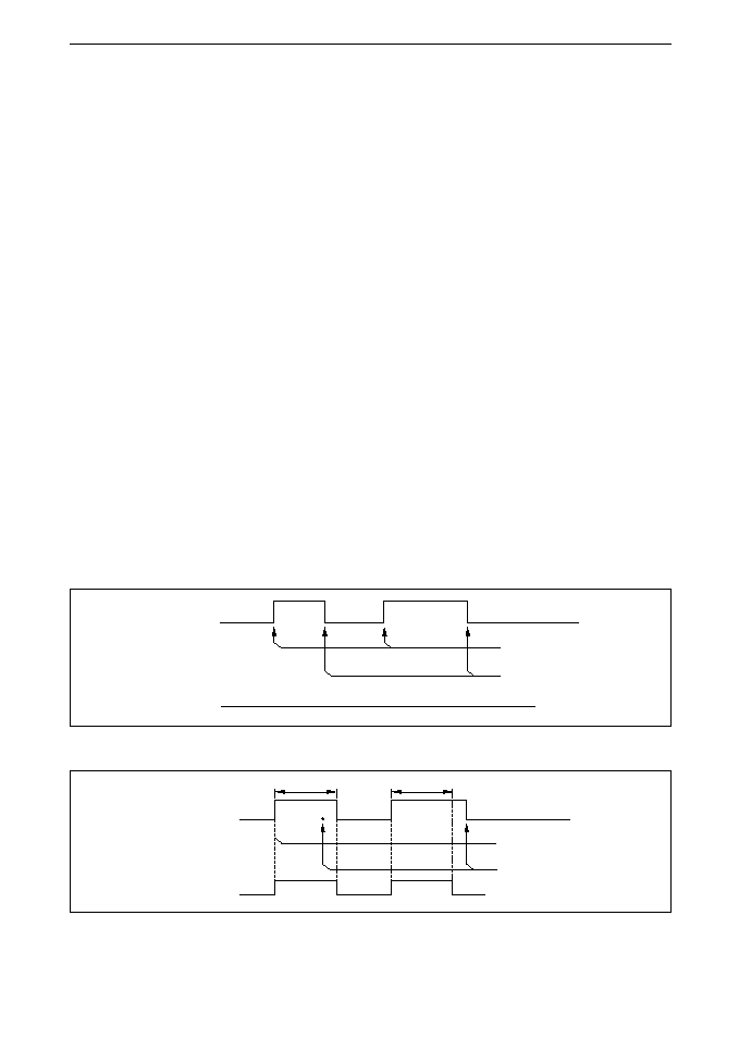
This output pin is N-channel open drain. It ORs the signals from the PERIODIC OUT
and ALARM OUT pins above.
Carry trigger
PERIODIC OUT
V
DD
Date and time
matching trigger
ALARM OUT
V
DD
INTERRUPT OUT
V
DD
Carry trigger
Date and time
matching trigger
° Semiconductor
MSM6542-01/02/03
81
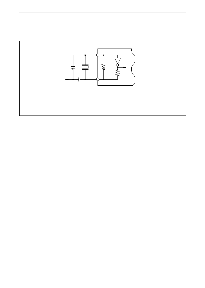
XT and XT (X'tal OSC)
These pins are the connecting terminals to connect the capacitors and crystal oscillator at
32.768kHz as shown below.
V
DD
or
GND
5M
TYP.
200K
TYP.
XT
32.768
kHz
C1
C2
XT MSM6542
Example
(Equivalent series resistance < 30 k
C
1
, C
2
= 15 to 30 pF)
Note:
Oscillation accuracy and allowable values of the equivalent series resistor for the
crystal oscillator depend on the value of the capacitor used for oscillation. For
selection of a crystal oscillator and the value of the capacitor needed for it,
consult the crystal oscillator manufacturer.
To supply external 32.768 kHz clocks, enter CMOS output or pulled-up TTL output to the XT
pin and leave the XT pin open.
V
DD
and V
SS
These are power supply pins. Connect the V
SS
pin to ground and supply positive power to the
V
DD
pin.
The 1 Hz, 30 sec ADJ, STOP/START, and 68/80 pins described below are used only for the
MSM6542-03.
1 Hz
This output pin is used to confirm the oscillation frequency. It outputs 1-Hz pluses at a duty
cycle of 50%.
This pin provides one-second output from the clock counter. Therefore, it is cleared to a low
when the REST bit is high or 30-second adjustment is performed. When STOP function is
performed, the output stops at whatever level the output is at that instant.
This pin provides CMOS output level, regardless of the level of the CS
1
pin. If a load is connected
to this pin during standby operation, the battery will be quickly dissipated.
=
° Semiconductor
MSM6542-01/02/03
82
30-sec ADJ (30-seconds Adjustment)
When this input pin goes high, 30-second adjustment is performed on the rising edge. When
not used, connect to ground.
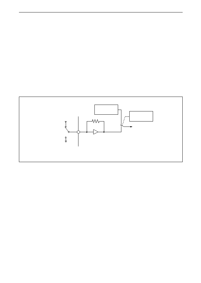
STOP/START
This input pin can be used as an integrating clock. When the pin is high, clocking at frequencies
lower than 4096 Hz stops. When the pin goes low, clocking is resumed.
The HD/SFT bit of the C
E
' register specifies whether the stop/start function is implemented by
hardware or software.
When not used, connect to ground. For more information, see the description of "C
F
register"
and "C
E
' register" in "EXPLANATION OF REGISTERS."
STOP
STOP bit of
the C
F
register
HD/SFT bit of
the C
E
' register
STOP/START
START
Equivalent circuit of the STOP/START pin
Inside of the MSM6542
68/80
This input pin selects which CPU this IC is to be connected. To connect the IC to the 68-based
CPU, leave the pin at V
DD
. To connect the IC to the 80-based CPU, leave the pin at the ground
level.

° Semiconductor
MSM6542-01/02/03
83
EXPLANATION OF REGISTERS
Registers R-S
1
, R-S
10
, R-MI
1
, R-MI
10
, R-H
1
, R-H
10
, R-D
1
, R-D
10
, R-MO
1
, R-MO
10
, R-Y
1
, R-Y
10
,
R-W
a)
The letter R followed by a hyphen (-) in these register names indicate a realtime register. S
1
,
S
10
, MI
1
, MI
10
, H
1
, H
10
, MO
1
, MO
10
, Y
1
, Y
10
, and W are abbreviations for Second 1, Second 10,
MInute 1, MInute 10, Hour 1, Hour 10, Day 1, Day 10, MOnth 1, MOnth 10, Year 1, Year 10,
and Week. The value of each register is weighted in BCD.
b)
Positive logic is used. For example, when (r-s
8
, r-s
4
, r-s
2
, r-s
1
) is (1, 0, 0, 1), it indicates 9
seconds.
c)
An asterisk (*) in bank 0 in the realtime register table indicates the bit is automatically set
at 0 even though the write data is 1, when the CAL bit of the C
E
' register is high.
When the CAL bit is low, registers R-D
1
, R-D
10
, R-MO
1
, R-MO
10
, R-Y
1
, and R-Y
10
are used as
RAM areas. The bits marked * in these RAM areas can be used for write and read
operations.
For more information, see the description of "C
E
' register" in "EXPLANATION OF REG-
ISTERS."
d)
Be sure not to set non-existent data in an non-RAM area, that is, realtime registers.
Otherwise, a clock error may occur.
e)
r-pm/am, r-h
20
, and r-h
10
In the 12-hour clock mode, the possible hours are from 1 A.M. to 12 A.M. and from 1 P.M.
to 12 P.M. When the bit is 1, it indicates P.M. When the bit is 0, it indicates A.M. In the 24-
hour clock mode, the possible hours are from 0 o'clock to 23 o'clock.
During write operation, the r-pm/am bit is ignored in the 24-hour clock mode and the r-
h
20
bit in the 12-hour clock mode.
During read operation, the r-pm/am bit is unconditionally set at 0 in the 24-hour clock
mode and the r-h
20
bit in the 12-hour clock mode.
f)
R-Y
1
and R-Y
10
The IC described in this manual operates in Gregorian years. When it operates in Japanese
calendar years (Heisei), a leap year is also automatically determined. Leap years are 1992,
1996, 2000, 2004, 2008, and so on.
° Semiconductor
MSM6542-01/02/03
84
r-w
4
Day of the week
0
0
0
0
1
1
1
r-w
2
r-w
1
0
0
1
1
0
0
1
0
1
0
1
0
1
0
Sun
Mon
Tue
Wed
Thu
Fri
Sat
g)
R-W
The R -W bits counts from 0 to 6. An example of weighting is shown in the following table.
Days are not determined from dates.
C
D
register (Control D Register)
a)
MASK
1
(D
0
)
This bit controls periodic output for which a carry from the clock counter is used as a trigger.
When the bit is 0, output is provided from the INTERRUPT OUT pin for the MSM6542-01/
02 or the PERIODIC OUT pin for the MSM6542-03. When the bit 1, output is disabled.
The relationships between causes of periodic output and the status of the MASK
1
bit are
shown below. (For the MSM6542-01/02, data resulting from the ORing of periodic output
and alarm output is output to the INTERRUPT OUT pin. For convenience, however, alarm
output is ignored in the following description.)
° Semiconductor
MSM6542-01/02/03
85
i)
In the periodic interrupt mode (when the IT/PLS
1
, bit is 1)
*1
When DP = 1, the open state is not entered until a certain period
passes after an interrupt is generated. (See the description of the C
E
register.)
*2
However, when DP = 1, if the IRQ FLAG
1
bit is read out within
122
Ķ
s after an interrupt is generated, it is cleared after 122
Ķ
s from the
generation of the interrupt.
ii)
In the periodic pulse output mode (when the IT/PLS
1
bit is 0.)
The open status is entered when the IRQ FLAG
1
is read. (*1)
No interrupt occurs
because the MASK
1
bit is 1.
Open
Low level
Interrupt timing
"0"
"0"
"1"
"1"
INTERRUPT OUT (-01, -02)
PERIODIC OUT (-03)
MASK
1
bit
When the IRQ FLAG
1
is read during masking,
IRQ FLAG
1
is not cleared. (*2)
When 0 is written in the IRQ FLAG
1
bit,
the open state is entered without having
to wait for automatic restration
The low level is not output
because the MASK
1
bit is 1.
Open
Low level
Output timing
"0"
"0"
"1"
MASK
1
bit
Automatic restoration
INTERRUPT OUT
(-01, -02)
PERIODIC OUT
(-03)
"1"
° Semiconductor
MSM6542-01/02/03
86
b)
MASK
2
(D
1
)
This bit controls the alarm output each time the contents of the clock counter match the date
and time for which an alarm is set. When the bit is 0, an alarm is output from the
INTERRUPT OUT pin for the MSM6542-01/02 or the ALARM OUT pin for the MSM6542-
3. When the bit is 1, alarm output is disabled.
The relationships between causes of alarm output and the status of the MASK
2
bit are shown
below. (For the MSM6542-01/02, data resulting from the OR-ing of periodic output and
alarm output is output to the INTERRUPT OUT pin. For convenience, however, periodic
output is ignored in the following description.)
i)
In the alarm interrupt mode (when the IT/PLS
2
bit is 1)
The open status is entered when the IRQ FLAG
2
is read. (*1)
A match for an alarm is not found
because the MASK
2
bit is 1.
Open
Low level
Match for an alarm
"0"
"0"
"1"
"1"
INTERRUPT OUT (-01, -02)
ALARM OUT (-03)
MASK
2
bit
When the IRQ FLAG
2
is read during masking,
IRQ FLAG
2
is not cleared. (*2)
*1
When DP = 1, the open state is not entered until a certain period
passes after an interrupt is generated. (See the description of the C
E
register.)
*2
However, when DP = 1, if the IRQ FLAG
2
bit is read out within
122
Ķ
s after an interrupt is generated, it is cleared after 122
Ķ
s from the
generation of the interrupt.
ii)
In the alarm pulse output mode (when the IT/PLS
2
bit is 0)
When the IRQ FLAG
2
bit is set at 0, the open state is
entered without having to wait for automatic
restration
The low level is not output
because the MASK
2
bit is 1.
Open
Low level
Match for an alarm
"0"
"0"
"1"
MASK
2
bit
Automatic restoration
INTERRUPT OUT
(-01, -02)
ALARM OUT
(-03)
"1"

° Semiconductor
MSM6542-01/02/03
87
c)
IT/PLS
1
(D
2
) (InTerrupt/PuLSe
1
)
This bit determines a mode for periodic output. When the bit is 1, a low-level interrupt
request is output from the INTERRUPT OUT pin for the MSM6542-01/02 or from the
PERIODIC OUT pin for the MSM6542-3. When the bit is 0, a low-level pulse is output. In
this case, the MASK
1
bit is 0. The output periods of interrupt output and pulse output are
determined by the setting of the C
D
' register.
d)
IT/PLS
2
(D
3
) (InTerrupt/PuLSe
2
)
This bit determines a mode for alarm output. When the bit is 1, a low-level alarm interrupt
request is output from the INTERRUPT OUT pin for the MSM6542-01/02 or from the
ALARM OUT pin for the MSM6542-03. When the bit is 0, a low-level pulse is output. In
this case, the MASK
2
bit is 0. When the contents of the alarm register match those of the
realtime counter within the range specified by the A-ENABLE register, an output wave-
form is provided.
In the alarm pulse output mode, the low level of a pulse lasts for about 61
Ķ
s.
C
E
register (Control E register)
a)
IRQ FLAG
1
(D
0
) (Interrupt ReQuest FLAG
1
)
The status of this bit depends on the hardware output, low or open, from the PERIODIC
OUT pin for the MSM6542-3 or INTERRUPT OUT pin which uses carry as a trigger for the
MSM6542-1/2. When hardware output is low, the bit is set at 1. When it is open, the bit
is set at 0.
The IRQ FLAG
1
bit is mainly used to indicate that there is an interrupt request for the
microcomputer. When the period set by the D
2
(CY
2
), D
1
(CY
1
), and D
0
(CY
0
) bits of the C
D
'
register expires with the D
0
(MASK
1
) bit of the C
D
register set at 0, output from the IN-
TERRUPT OUT pin changes from open to low. At the same time, the IRQ FLAG
1
bit
changes from 0 to 1.
When the D
2
(IT/PLS
1
) bit of the C
D
register is 1 (interrupt mode), the IRQ FLAG
1
bit remains
at 1 (hardware output is low) until the bit is read. When the bit is read, it is cleared.
However, when the IRQ FLAG
1
bit is read whithin about 122
Ķ
s of occurrence of an
interrupt with the D
0
(DP) bit of the C
E
' register set at 1, the IRQ FLAG
1
bit is not cleared
immediately. It is cleared about 122
Ķ
s after the interrupt occurs. When the bit is read at
least about 122
Ķ
s after an interrupt occurs, it is cleared immediately.
In the interrupt mode, writing 0 in the IRQ FLAG
1
bit does not clear the bit. When another
interrupt occurs with the bit set at 1, it is ignored.
When the D
2
(IT/PLS
1
) bit of the C
D
register is 0 (periodic pulse output mode), the IRQ
FLAG
1
bit remains at 1 (hardware output is low) until 0 is written in the bit or the automatic
restoration time determined by the period set by the D
2
(CY
2
), D
1
(CY
1
), and D
0
(CY
0
) bits
of the C
D
' register expires. When the IRQ FLAG
1
bit is read in the periodic pulse output
mode, it is not cleared.
° Semiconductor
MSM6542-01/02/03
88
i)
In the interrupt mode (when the IT/PLS
1
bit is 1)
(i-1)
When DP is 0:
The IRQ FLAG
1
bit is read
Interrupt timing
"0"
"1"
"0"
IRQ FLAG
1
IRQ FLAG
0
(i-2)
When DP is 1:
The IRQ FLAG
1
bit is read
Interrupt timing
"0"
"1"
"0"
IRQ FLAG
1
IRQ FLAG
0
122Ķs
122Ķs
"1"
Note:
When the IRQ FLAG
1
bit is read within the 122
Ķ
s interval with the MASK
1
bit set at 1, it is not
cleared. The IRQ FLAG
1
bit is cleared after the
122
Ķ
s interval ends.
ii)
In the periodic pulse output mode (when the IT/PLS
1
bit is 0)
0 is written in the IRQ FLAG
1
bit
with DP set at 0
Output timing
"0"
"1"
"0"
IRQ FLAG
2
IRQ FLAG
0
Automatic restoration
° Semiconductor
MSM6542-01/02/03
89
b)
IRQ FLAG
2
(D
1
) (Interrupt ReQuest FLAG
2
)
The status of this bit depends on the hardware output, low or open, from the ALARM OUT
pin for the MSM6542-03 or INTERRUPT OUT pin which uses a match with a set alarm time
as a trigger for the MSM6542-01/02. When hardware output is low, the bit is set at 1. When
it is open, the bit is set at 1.
The IRQ FLAG
2
bit is mainly used to indicate that there is an alarm timer interrupt for the
microcomputer. When the time set by alarm registers, A-S
1
to A-W, and the A-ENABLE
register expires with the D
1
(MASK
2
) bit of the C
D
register set at 0, hardware output changes
from open to low. At the same time, the IRQ FLAG
2
bit changes from 0 to 1.
When the D
3
(IT/PLS
2
) bit of the C
D
register is 1 (alarm interrupt mode), the IRQ FLAG
2
bit
remains at 1 (hardware output is low) until the bit is read. When the bit is read, it is cleared.
However, when the IRQ FLAG
2
bit is read within about 122
Ķ
s of occurrence of an alarm
interrupt with the D
0
(DP) bit of the C
E
' register set at 1, the IRQ FLAG
2
bit is not cleared
immediately. It is cleared about 122
Ķ
s after the interrupt occurs. When the bit is read at
least about 122
Ķ
s after an interrupt occurs, it is cleared immediately.
In the alarm interrupt mode, writing 0 in the IRQ FLAG
2
bit does not clear the bit. When
another interrupt occurs with the bit set at 1, it is ignored.
When the D
3
(IT/PLS
2
) bit of the C
D
register is 0 (alarm pulse output mode), the IRQ FLAG
2
bit remains at 1 (hardware output is low) until 0 is written in the bit or automatic restoration
is performed about 61
Ķ
s later. When the IRQ FLAG
2
bit is read in the alarm pulse output
mode, it is not cleared.
i)
In the alarm interrupt mode (when the IT/PLS
2
bit is 1)
(i-1)
When DP is 0:
(i-2)
When DP is 1:
The IRQ FLAG
2
bit is read
Alarm interrupt timing
"0"
"1"
"0"
IRQ FLAG
2
IRQ FLAG
0
The IRQ FLAG
2
bit is read
Alarm interrupt timing
"0"
"1"
"0"
IRQ FLAG
2
IRQ FLAG
0
122Ķs
122Ķs
"1"
Note:
When the IRQ FLAG
2
bit is read within the 122
Ķ
s interval with the
MASK
1
bit set at 1, it is not cleared. The IRQ FLAG
2
bit is cleared after
the 122
Ķ
s interval ends.
° Semiconductor
MSM6542-01/02/03
90
ii)
In the alarm pulse output mode (when the IT/PLS
2
bit is 0)
0 is written in the IRQ FLAG
2
bit
with DP set at 0
Output timing
"0"
"1"
"0"
IRQ FLAG
2
IRQ FLAG
0
Automatic restoration
61Ķs
c)
REST (D
2
) (RESeT)
This bit resets the less-than-second counter. While the bit is 1, the counter is being reset.
When 0 is written in the bit, reset is canceled.
When CS
1
goes low, the REST bit is automatically set at 0. When 1 is written in the bit, the
TEST
1
and TEST
2
bits of the C
C
' register are also set at 0.
d)
IRQ FLAG
0
(D
3
) (Interrupt ReQuest FLAG
0
)
This bit indicates whether the extended time zone for interrupt output is in progress when
the DP is 1. The bit is set at 1 when: (1) the D
2
(IT/PLS
1
) bit of the C
D
register is 1 (periodic
interrupt mode) or the D
3
(IT/PLS
2
) bit of the C
D
registe is 1 (alarm interrupt mode), (2) the
D
0
(DP) bit of the C
E
' register is 1 (data protect mode), and (3) 122
Ķ
s (extended time zone)
do not elapse after a periodic interrupt or an alarm interrupt occurs. When 122
Ķ
s elapse
after occurrence of such an interrupt, the bit is automatically set at 0.
The bit is not cleared when it is read. Also, data cannot be written in the bit.
C
F
Register (Control F Register)
a)
READ FLAG (D
0
)
This bit indicates a one-second carry. It is used to read time data.
When the READ FLAG bit is read, it is reset at 0. The status lasts until the less-than-second
realtime counter generates a carry to the one-second counter.
When a carry to the one-second realtime counter is generated, the READ FLAG bit is set at
1. The status lasts until the bit is read.
When a carry to the one-second realtime counter is generated with the READ FLAG bit set
at 1, the bit remains unchanged, i.e., at 1.
The READ FLAG bit is also set at 1 when 30-s adjustment is performed by software or
hardware. The status last until the bit is read.
For the usage of the READ FLAG bit, see "Reading registers" in reference flowcharts.

° Semiconductor
MSM6542-01/02/03
91
b)
30-s ADJ (D
1
) (30-s ADJustment)
When 1 is written in this bit, software makes a 30-s adjustment. For 125
Ķ
s after this writing,
registers R-S
1
to R-W (at addresses 0 to C in bank 0 in the register table) cannot be read or
written due to limitations to the inside of the IC. When the CAL bit of the C
E
' register is 0,
however, registers R-D
1
to R-Y
10
(at addresses 6 to B in bank 0) which can be used as RAM
are as can be read or written during 30-s adjustment. The bit remains at 1 for up to 250
Ķ
s
after 1 is written in the bit. Then, the bit is automatically reset at 0. Confirm that the bit is
automatically reset at 0 before manipulating registers R-S
1
to R-Y
10
and R-W (when CAL is
0, R-S
1
to R-H
10
and R-W).
The 30-s ADJ bit is also set at 1 when hardware makes a 30-s adjustment. In this case too,
confirm that the bit is automatically reset at 0 before manipulating registers R-S
1
to R-Y
10
and R-W (when CAL is 0, R-S
1
to R-H
10
and R-W).
When the 30-s ADJ bit is set at 1, the D
0
(READ FLAG) of the bit C
F
register is also set at 1.
c)
STOP (D
2
)
This bit is used for the integrating clock operated by software. When the bit is set at 1,
clocking at 4096 Hz and lower stops. When the bit is set at 0, clocking is resumed.
For the MSM6542-3, the HD/SFT bit of the C
E
' register can be used to select hardware or
software to implement the stop/restart function.
d)
BANK 1/0 (D
3
)
When this bit is set at 1, bank 1 is selected. When it is set at 0, bank 0 is selected. The bit can
be set even in the data protect mode.
Registers A-S
1
, A-S
10
, A-MI
1
, A-MI
10
, A-H
1
, A-H
10
, A-D
1
, A-D
10
, A-MO
1
, A-MO
10
, A-W
a)
The letter A followed by a hyphen (-) in these register names indicate an alarm register. S
1
,
S
10
, MI
1
, MI
10
, H
1
, H
10
, MO
1
, MO
10
, and W are abbreviations or Second
1
, Second
10
, MInute
1
,
MInute
10
, Hour
1
, Hour
10
, Day
1
, Day
10
, MOnth
1
, MOnth
10
, and Week. The value of each
register is weighted in BCD.
b)
The positive logic is used. For example, when (a-s
8
, a-s
4
, a-s
2
, a-s
1
) is (1, 0, 0, 1), it indicates
9 seconds.
c)
An asterisk (*) in the alarm register table indicates the bit automatically set at 0 even though
the write data is 1. This is true when the alarm register is in the alarm setting range set by
the A-ENABLE register.
The registers outside the alarm setting range set by the A-ENABLE register are used as
RAM areas. The bits marked * in these RAM areas can be used for write and read
operations.
For more information, see the descriptions of "A-ENABLE."
d)
Be sure not to set non-existing data in alarm registers in the alarm setting range. Otherwise,
an alarm may not be generated.

° Semiconductor
MSM6542-01/02/03
92
e)
a-pm/am, a-h
20
, and a-h
10
In the 12-hour clock mode, the possible hours are from 1 A.M. to 12 A.M. and from 1 P.M.
to 12 P.M. When the bit is 1, it indicates P.M. When the bit is 0, it indicates A.M. In the 24-
hour clock mode, the possible hours are from 0 o'clock to 23 o'clock.
In the 12-hour clock mode, the a-h
20
bit is write-enabled. When 1 is written in it, an alarm
indicating an impossible time is generated. This is also true for the other registers: when
an impossible alarm time is set, no alarm is generated.
In the 24-hour clock mode, the a-pm/am bit is read- and write-enabled but its status is
assumed to be always the same as that of the r-pm/am bit.
f)
A-W
The A-W bits use the numbers from 0 to 6. Weight these bits in the same way as for R-W.
g)
The alarm registers are not incremented or decremented
A-ENABLE Register (Alarm ENABLE)
This register sets a comparison range for the real time counter and alarm registers.
The alarm registers outside the comparison range can be used as four-bit RAM areas. (The bits
marked an asterisk (*) in the register table can be used for write and read operations. When DP
is 1, however, write operation is not possible.)
The following table shows the relationships between the status of the A-ENABLE register bits
and alarm comparison ranges.

° Semiconductor
MSM6542-01/02/03
93
ae8
Alarm comparlson range
0
1
2
3
4
5
6
7
8
9
A
B
C
D
E
F
0
0
0
0
0
0
0
0
1
1
1
1
1
1
1
1
None
A ~ S
1
A-S
1
~ A-S
10
A-S
1
~ A-MI
1
A-S
1
~ A-MI
10
A-S
1
~ A-H
1
A-S
1
~ A-H
10
A-S
1
~ A-D
1
A-S
1
~ A-D
10
A-S
1
~ A-MO
1
A-S
1
~ A-MO
10
A-S
1
~ A-H
10,
A-W
A-S
1
~ A-D
1,
A-W
A-S
1
~ A-D
10,
A-W
A-S
1
~ A-MO
1,
A-W
A-S
1
~ A-MO
10,
A-W
ae4
ae2
ae1
0
0
0
0
1
1
1
1
0
0
0
0
1
1
1
1
0
0
1
1
0
0
1
1
0
0
1
1
0
0
1
1
0
1
0
1
0
1
0
1
0
1
0
1
0
1
0
1
C
C
' Register (Control C' Register)
This register is a test register. The user can use it when both the TEST
1
(D
0
) and TEST
2
(D
1
) bits
of the register are 0. When either or both TEST bits are 1, Oki's test functions are enabled, making
the execution results of user's functions unpredictable.
When the register is read, it is automatically cleared. The read value is always 0. When 1 is
written in the REST (D
2
) bit of the C
E
register, the C
C
' register is automatically set at 0.
C
D
' Register (Control D' Register)
This register sets an interrupt period when the IT/PLS
1
(D
2
) bit of the C
D
register is 1 and a pulse
output period when the bit is 0. The following table shows the relationships between the status
of the C
D
' register bits and the length of periods.
° Semiconductor
MSM6542-01/02/03
94
CY
0
Duty cycle of the low level
when IT/PLS1 = 0
0
0
0
0
1
1
1
1
CY
2
CY
1
1/2
1/2
1/2
1/2
1/2
1/8192
1/491520
1/4915200
0
0
1
1
0
0
1
1
0
1
0
1
0
1
0
1
Period
1/1024 s
1/128 s
1/64 s
1/16 s
1/2 s
1 s
1 min
10 min
C
E
' Register (Control E' Register)
a)
DP (D
0
) (Data Protect bit)
This bit has the following two functions:
i)
Restricts write operation to the IC.
ii)
Prolongs the resetting of the IRQ FLAG
1
bit when the bit is read within 122
Ķ
s
of occurrence of a periodic alarm in the periodic interrupt mode. Also prolongs
the resetting the IRQ FLAG
2
bit in the same way in the alarm interrupt mode.
i)
Restriction of write operation
When the DP bit is 0, normal write operation is enabled. When the bit is 1, however,
the IC is write-protected except the BANK 1/0 (D
3
) bit of the C
F
register for which
write operation is always allowed.
The DP bit is designed to protect the registers from extenal noise, particularly
erroneous write signal noise which is generated when the standby power supply
voltage is switched to the system power supply voltage or vice versa. After the
necessary data is written, it is recommended that the DP bit be set at 1 if only read
operation is performed.
ii)
Prolongation of reset of the IRQ FLAG bits
When the IT/PLS
1
(D
2
) bit of the C
D
register is 1 (periodic interrupt mode) with the DP
bit set at 0, reading the C
E
register clears the IRQ FLAG
1
bit. This is also true for the
IT/PLS
2
(D
3
) bit when it is 1 (alarm interrupt mode): reading C
E
register clears the IRQ
FLAG
2
bit.
When the IRQ FLAG
1
bit is read within about 122
Ķ
s of occurrence of an interrupt with
the IT/PLS
1
(D
2
) bit of the C
D
register set at 1 (periodic interrupt mode), the IRQ FLAG
1
bit is not cleared immediately. Similarly, the IRQ FLAG
2
bit is not cleared immediately
when the IT/PLS
2
(D
3
) bit is 1 (alarm interrupt mode). These IRQ FLAG bits are
cleared about 122
Ķ
s after an interrupt occurs. When these bits are read at least about
122
Ķ
s after an interrupt occurs, they are cleared immediately. For more information,
see the description of "C
E
REGISTER."
° Semiconductor
MSM6542-01/02/03
95
When an IRQ FLAG bits are read mistakenly due to external noise, particularly
erroneous read signal noise which is generated when the standby power supply
voltage is switched to the system power supply voltage or vice versa, therefore, the
IRQ FLAG bits are not cleared immediately but read at the correct times.
When 1 is written in the DP bit, the bit is immediately set at 1 except the following two
cases.
(i)
The CS
1
bit is low.
(ii)
For 62
Ķ
s immediately after the DP bit changes from 1 to 0.
Writing 0 in the DP bit, that is, canceling data protection is allowed only when:
(i)
Zero is written in the DP bit more than 2 ms after CS
1
changes from low to high.
(ii)
The CS
1
bit is high 11 ms after 0 is written in the DP bit.
b) CAL (D
1
) (CALendar)
This bit specifies a range in which the realtime counter is incremented. When the bit is 1,
the R-S
1
to R-Y
10
and R-W register can be incremented. When the bit is 0, the R-S
1
to R-H
10
and R-W registers can be incremented.
With the CAL bit set at 1, R-D
1
to R-Y
10
are used as realtime registers. Therefore, setting an
impossible time in these registers causes an error. For the bits marked an asterisk (*) of the
R-D
10
and R-MO
10
registers in the register table, when 1 is written, 0 is automatically set. The
alarm comparison range is specified by the A-ENABLE register.
When the CAL bit is 0, the R-D
1
to R-Y
10
registers are not incremented. They can be used as
static RAM, enabling arbitrary values to be set. The bits marked an asterisk (*) of the R-D
10
and R-MO
10
registers in the register table can be subject to both write and read operations.
The alarm comparison range is specified by the A-ENABLE register. However, the R-D
1
to
R-Y
10
registers are assumed to always provide a match. When these registers are used as
static RAM, they cannot be rewritten when the DP bit is 1.
CS
1
Data protection can be canceled
because CS
1
is high
0 is written
in the DPbit
DPbit
1 is written
in the DPbit
11ms
1 written in the DPbit
in this period is ignored
62Ķs

° Semiconductor
MSM6542-01/02/03
96
c) 24/12 (D
2
) (24-hour clock/12-hour clock)
This bit selects a 24-hour clock or 12-hour clock mode. When the bit is 1, the 24-hour clock
mode without PM/AM specification is enabled. When the bit is 0, the 12-hour clock mode
with PM or AM specified is enabled.
When the 24/12 bit is rewritten, data in the R-H
1
register and higher will be destroyed. The
data needs to be written again.
d) HD/SFT (D
3
) (HarDware/SoFTware)(This bit applicable only to the MSM6542-03)
This bit determines which mode, hardware or software, is enabled to validate the stop/start
function. When the bit is 1, hardware enables the stop/start function (pin 20). When the bit
is 0, software enables the stop/start function (D
2
of the C
F
register)
The stop/start function by hardware and that by software cannot be used at the same time.
For the MSM6542-01/02, the stop/start function by software is always enabled due to an
internal setting on the IC. However, the HD/SFT bit can be read or written to freely
regardless of this setting, enabling the bit to be used as a memo bit.
° Semiconductor
MSM6542-01/02/03
97
USAGE
Pattern layout
The oscillation stage of the 32.768 kHz oscillator circuit is at a high impedance to achieve very
low power dissipation. In addition, since sine waves are produced at as low as 32.768 kHz,
oscillation waves stay near the threshold for a longer time. For this reason, countermeasures
must be taken against power supply noise and external noise from the viewpoint of an analog
IC.
Countermeasures against power supply noise
Insert a 4.7
Ķ
F tantalum capacitor and 0.01
Ķ
F ceramic capacitor as close to the IC as possible.
When another IC (for example, backup RAM) is used in the battery-backed circuit, also insert
a by pass capacitor in that IC.
Countermeasures against external noise
Place the crystal for the oscillator circuit and the capacitors as close to the IC as possible. Do not
route other signal lines in the oscillator circuit regardless of whether the oscillator circuit is
placed on the front or back of the PC board.
Sufficiently separate the XT and XT signal lines from the other signal lines regardless of whether
these signal lines are running on the fron or back of the PC board (see a.. and b.. of the figure
below).
For the MSM6542-01/02
For the MSM6542-03
V
DD
XT XT
a
b
2
1
1
7.5 mm
5 mm
2
From V
SS
pin
Pass
capacitor
V
DD
XT XT
a
b
2
1
1
0.3 INCH
0.2 INCH
2
From pin 12 (V
SS
)
NC
Enclose the V
DD
line oscillation
section
V
DD
XT XT
a
b
2
1
From V
SS
pin
Bypass
capacitor
V
DD
XT XT
a
b
2
1
From pin 12 (V
SS
)
NC
Bypass
capacitor
° Semiconductor
MSM6542-01/02/03
98
Sample connection to a microcomputer
Various microcomputers are upgraded day by day. Updated versions of this data sheet may not
be capable of keeping pace with this progress. Check the matching of switching characteristics
in advance.
MSC51
MSM6542
Decoder
D
3
D
2
D
1
D
0
A
3
A
2
A
1
A
0
CS
0
RD
WR
RD
WR
ALE
3
2
1
0
PORT
PORT
4 ~ 7
ALE
MC6809
MSM6542
Decode
r
D
3
D
2
D
1
D
0
D
3
D
2
D
1
D
0
A
3
A
2
A
1
A
0
A
3
A
2
A
1
A
0
CS
0
ALE
V
DD
A
4
~ A
15
E
R/
W
E
R/
W
[MCS51]
[MC6809]
Decoder
D
3
D
2
D
1
D
0
D
3
D
2
D
1
D
0
A
3
A
2
A
1
A
0
A
3
A
2
A
1
A
0
CS
0
RD
WR
V
DD
G1
G2
A
4
~ A
15
IORQ
or
MREQ
RD
WR
ALE
[For the Z80]
Note:
Select either IORQ or MREQ so that
the Z80 switching characteristics
determined by the crystal oscillator
for the Z80 match those of the IC
described in this data sheet.
° Semiconductor
MSM6542-01/02/03
99
Sample peripheral circuits
Before using sample peripheral circuits shown below, check them against the user's system.
Power supply circuit (Place a bypass capacitor as close to the IC as possible.)
[When power is supplied from the +5V power supply]
+5.1V
A495
V
CE (sat)
= 0.1V
4.7ĶF
Tantalum capacitor
V
DD
V
SS
MSM6542
+ +
0.01Ķ
Ceramic
capacitor
+
22Ķ
R*
10K
51K
10K
C372
1.2 x 3 = 3.6V
Cadmium battery
When the power supply is turned off, inverse current
flows temporarily from the collector of the A495 transistor
to the emitter. To deal with this problem, use a large
value capacitance.
R*: For less than charge current limit
IS1588
V = 0.69V
F
+5.7V
Alternative circuit
R
4.7Ķ
+
0.01Ķ
V
DD
GND
MSM6542
Tantalum
capacitor
Ceramic
capacitor
Lithium battery
R:
Limit resistance to conform to the UL standard.
The value depends on the nominal capacity of the
battery used. Consult the battery manufacture.
C372
VF = 0.69V
or
Schottky diode
Main power
supply (5V)
Main power
supply (5V)
One-chip
voltage
detector
IC
V
DD
V
SS
CS
1
MSM6542
This circuit detects a rough voltage level.
It is suitable for a system for which the DP
bit is set at 1.
V
DD
V
SS
CS
1
MSM6542
Sample main power supply monitor circuit
° Semiconductor
MSM6542-01/02/03
100
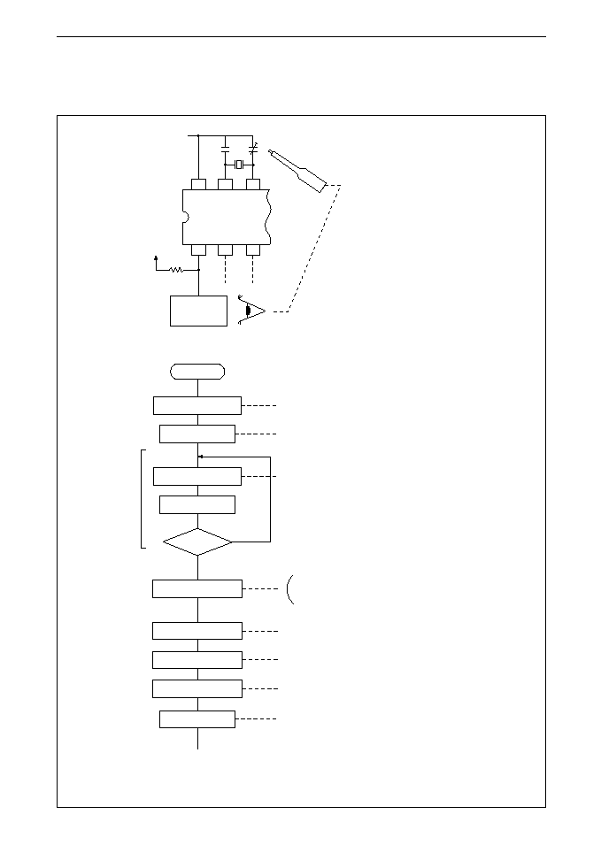
Oscillation frequency adjustment
[For the MSM6542-01/02]
18
17
16
3
2
1
INTERRUPT
OUT
V
DD
XT
XT
Screwdriver used
for adjustment
Eye
V
DD
3.3 ~ 10K
Frequency
counter
Turn on power
C
F
(1, 0, 0, 0)
Read C register
C'
C
E'
(X, X, X, 0)
Read C
E'
register
DP = 0 ?
N
Y
*1
C
D'
(0, CY
2
, CY
1
, CY
0
)
C
F
(0, 0, 0, 0)
C
E
(0, 0, 0, 0)
C
D
(0, 1, 1, 0)
Read C
E
register
*2
To the next page
Banks are switched
∑ X for (D
3
, D
2
, D
1
, D
0
) is a Don't Care bit
Dummy read to clear the test bits
Procedure for canceling data protection
Set a frequency of the signal to be output from pin 1.
Examples 64 Hz: (0 0 1 0) (duty cycle: 1/2)
1 Hz: (0 1 0 1) (duty cycle: 1/8192)
Banks are switched. The stop bit is cleared.
The reset bit is cleared
Preparation for a carry (oscillation).
When an alarm occurs, a carry is inhibited.
Dummy read to clear the IRQ FLAG bit
1
° Semiconductor
MSM6542-01/02/03
101
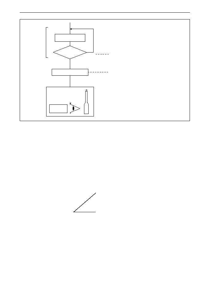
Frequency
counter
Eye
Frequency adjustment
C
D
(0, 0, 1, 0)
Read C
E
register
*3
IRQ FLAG = 1 ?
1
A carry (oscillation) is checked
Output of a signal at the frequency set by C
D'
is command through pin 1.
N
Y
*1 To cancel data protection, oscillation must be in progress. It takes about 13 ms (2 ms
during which the writing of DP
0 is inhibit in the rising of CS
1
plus 11 ms required until
DP = 0 is executed.) This loop includes a wait time before oscillation starts. Usually, the
loop takes 0.5 to 2 seconds. When the power is turned on, the value of the DP bit is
unpredictable. When the value is 0 incidentally, the loop does not return.
*2, 3
The IRQ FLAG
1
is cleared at the step marked *2. If IRQ FLAG
1
= 1 is detected in the loop
marked *3, therefore, it means that original oscillation is divided.
Other notes
Possible causes why the loop marked *1 or *3 becomes endless
Yes
∑
Incorrect programming
∑
The frequency counter is not adjusted.
Observe the waveform at pin 1 on an
oscilloscope.
Oscillation waveform at XT
No
∑
Oscillation is impeded by a leak due to
a dirty PC board. Clean the PC board.
∑
The capacitance of the capacitor for
oscillation is inadequate. Consult the
crystal manufacturer.
∑
Defective crystal oscillator or IC. Re-
place it.

° Semiconductor
MSM6542-01/02/03
102
Possible causes when the loop marked *1 or *3 takes a long time (2 or 3 seconds or more)
∑ Oscillation is impeded by a leak due to a dirty PC board. Clean the PC board.
∑ The capacitance of the capacitor for oscillation is inadequate. Consult the crystal
manufactuer.
Possible causes why the frequency counter is not stable.
∑ The frequency counter is not adjusted. Observe the waveform at pin 1 on an oscilloscope.
∑ The pattern layout is incorrect. See the description of "Pattern layout." Insert a bypass
capacitor having a capacitance of at least 1
Ķ
F between the V
DD
and V
SS
pins.
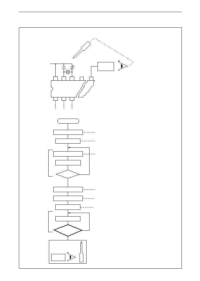
° Semiconductor
MSM6542-01/02/03
103
For the MSM6542-03
For the notes for "1, "2 and "3 and other notes
are same as for the MSM6542-01/02.
Frequency
adjustment
(1Hz)
Banks are switched
Read C
F
register
Read C
F
register
Dummy read to clear the test bits
Procedure for canceling data protection
Banks are switched. the stop bit is cleared
The reset bit is cleared
Dummy read to clear the IRQ FLAG bits
C
F
(1, 0, 0, 0)
Read C
E'
register
C
E'
(X, X, X, 0)
C
F
(0, 0, 0, 0)
C
E
(0, 0, 0, 0)
*2
*1
N
Frequency
counter
Frequency
counter
Screwdriver used
for adjustment
Eye
Eye
Y
Y
*3
READ FLAG=1?
22
23
24
21
DP =0?
2
1
3
XT
XT
V
DD
Turn on power
1Hz
17
Read C
C'
register
N
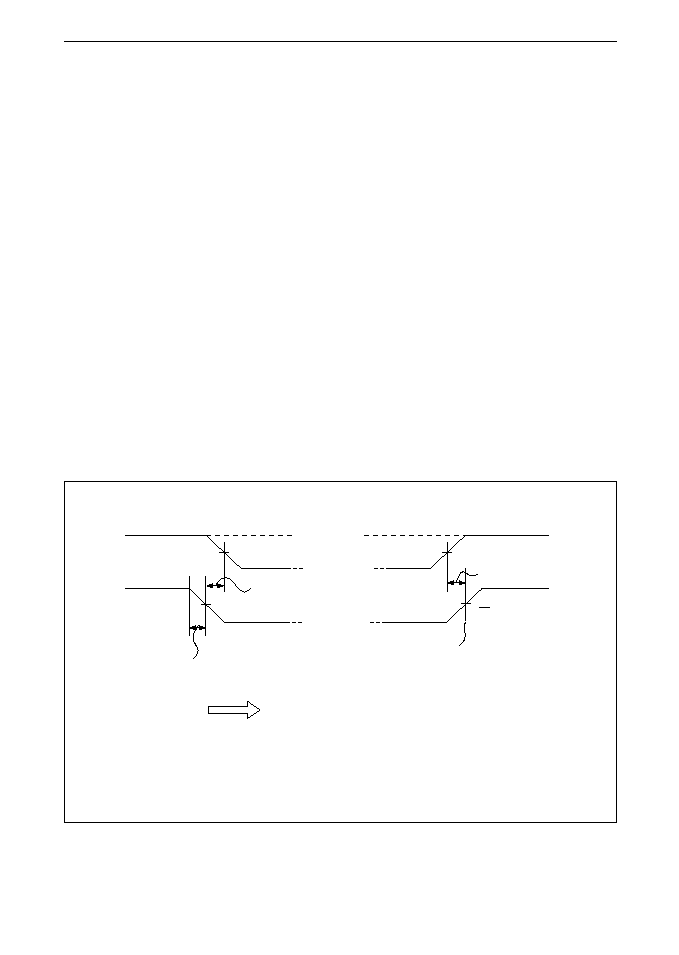
° Semiconductor
MSM6542-01/02/03
104
Use of CS
1
V
IH
and V
IL
of CS
1
has the following three functions:
1.
Validate the interface with the microcomputer when 5V power is used.
2.
Inhibit use of the control bus, data bus, and address bus and prevent through-current
specific to CMOS input in the standby mode.
3.
Protect register data of the IC when the standby mode is entered or exited.
To implement these functions:
1.
To validate the interface with the microcomputer when 5V power is used, input must be
at least 4/5 V
DD
.
2.
When the mode is switched to the standby mode, input must be 1/5 V
DD
or less to inhibit
use of the buses. In the standby mode, input must be nearly 0V to prevent through-current.
3.
When the standby mode is entered or exited, the main power and CS
1
must conform the
following timing charts:
Note:
In the standby mode, the operating power supply voltage is from 4V to 2V (minimum
value). Clocking is performed but the interface to the outside of the IC is not assured.
When a system is implemented with DP = 0:
Exiting from the standby mode
4 ~ 6V
4 ~ 4.5V*
1Ķs(MIN)
1Ķs(MIN)
Main power
supply (5V)
4 ~ 4.5V*
CS
1
Switching to the standby mode
POWER OFF
4
5 V
DD
1
5 V
DD
(V
DD
for the IC described in
this data sheet is 2 to 6 V.)
During the period,
CS
0
of the IC
is high or
WR is not generated.
4 to 4.5V* are measures of the minimum 5-V
main power supply voltage at which the CPU
does not assure correct program operations.
This is also the for the following timing chart:
The purpose is to maintain data in
static RAM in the standby mode.
0V
On and after this period, the interface
through the IC is possible
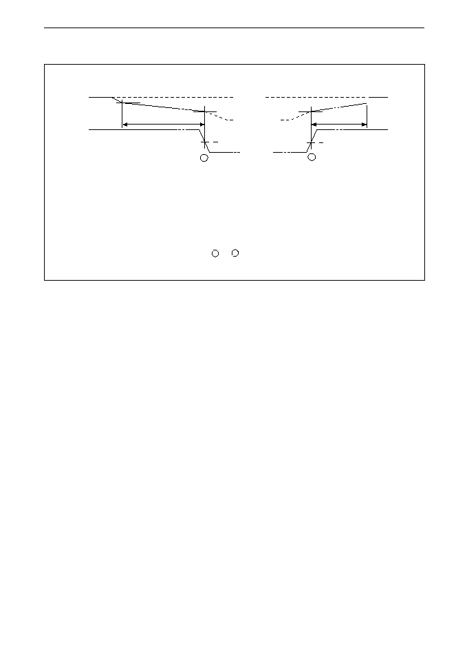
° Semiconductor
MSM6542-01/02/03
105
When a system is implemented with DP = 1:
Switching to the standby mode
Existing from the standby mode
POWER OFF
* 2
2 V or more
2 V or more
4 ~ 6V
4 ~ 4.5V
Main power
supply
(4 ~ 4.5V)
CS
1
4
5 V
DD
1
5 V
DD
a
*1
0V
b
*1, *2:
∑
The duration in this interval must be 8.7 ms or less.
∑
Through current at the input stage (A
0
~ A
3
, D
0
~ D
3
, control inputs) caused by intermediate voltage
input level and bus charge current cuaused by not programmed read out operation of CPU will
dissipate power source.
Therefore, it is recommended that the voltage for monitoring the power supply of the CS1 control
system be higher than the main power supply/battery switching voltage so that battery backup is
enabled only in the interval from a .. to b .. .
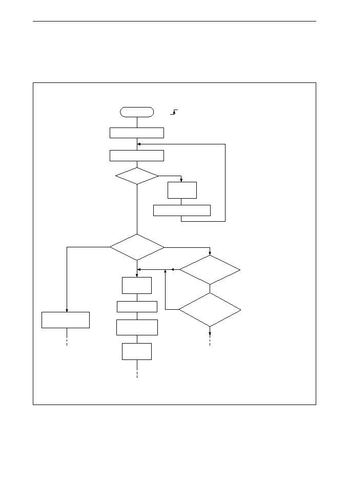
° Semiconductor
MSM6542-01/02/03
106
Reference flowcharts
In the following flowcharts, description of bank switching is omitted.
[Power on sequence when DP is 0]
Apply 5V
Read C register
C'
N
Y
*1
*2
C
E'
register
DP
0
Idling for at least 11ms
DP = 0
Read C
E'
register
What status
before 5V is
applied?
*3
Are contents of
individual register
correct
Does operator
determine that the
current time is
correct
C
E
register
REST
1
Idling for 123 Ķs
Set individual
registers
Check contents of
individual register
C
E
register
REST
0
Standby
Unclear
No
Yes
V
DD
= 0V
Yes
*4
*5
No
(CS
1
)
The test bit is cleared.
Time until the DP bit becomes
0 under assumption that oscil-
lation is in progress.
When the voltage before 5V is
applied is 0V, this loop takes
the time equal to the one re-
quired to start oscillation.
Usually, it takes 0.5 to 2 s.
The contents of R-S, to R-Y
10
and R-W must be possible
values and the values of the
other registers must be as
expected.
Wait time until a carry which
may be generated is com-
pleted.
*1
*2
*3
*4
*5
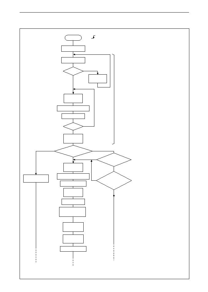
° Semiconductor
MSM6542-01/02/03
107
[Power on sequence when DP is 1]
Apply 5V
Read C
C'
register
DP = 1 ?
C
E'
register
DP
0
C
E'
register
DP
1
Idling for at least 11ms
Read C
'
register
E
Read C
E'
register
Check contents of
individual registers
DP = 0 ?
C
E'
register
DP
1
Standby
Unclear
What status before
5V is applied?
C
E'
register
DP
1
Are connents of
individual register
correct?
Does operator
determine that the
current time is
is correct?
Idling fore at least 11ms
Check that DP is 0
Idling for 125 Ķs
Set individual
registers
C
E
register
REST
0
Check that DP is 1
N
Y
*3
N
*5
Y
No
*3
Yes
Yes
No
*4
*4
(CS
1
)
V
DD
= 0V
*1
C
E
register
REST
1
C
E'
register
DP
1
*1 The test bit is cleared.
*2 It takes 9 to 11 ms from when
0 is written in the DP bit to
when it is set at 0 in the IC. If
0 is written unintentionally in
the DP bit during application
of 5V power, it may be set at 0.
To prevent this, first set the
DP bit at 0 then at 1. When the
voltage before 5V is applied is
0V, this loop takes the time
equal to the one required to
start oscillation. Usually, it
takes 0.5 to 2 s.
*3 Time until the DP bit becomes
0 under assumption that os-
cillation is in progress.
*4 The contents of R-S1, to R-
Y10 and R-W must be pos-
sible values and the values of
the other registers must be as
expected.
*5 Wait time until a carry, which
may be generated, is com-
pleted.
° Semiconductor
MSM6542-01/02/03
108
[Temporarily canceling DP = 1 in a system for which DP is set at 1]
Idling
Read C
'
register
E
DP = 0?
Rewrite individual
registers
Idling
DP = 1
* 2
* 3
* 1
* 2
N
* 3
N
Y
DP 0
DP 1
OR
Read C
E'
register
Idling for at least 11ms
Check that DP is 0
Rewrite individual
registers
Idling
* 1
DP 1
DP 0
Y
*1
Time until the DP bit becomes 0 under assumption that
oscillation is in progress.
*2
See "Rewriting individual register."
*3
Writing 1 in it is inhibited for 62
Ķ
s after the DP bit is set
at 0. This idling is provided to make the DP bit wait to be
set at 1.
*1
Processing by other IC or wait time to prevent unneces-
sary readouts which occur frequently. A measure is 1 ms.
*2
See "Rewriting individual register."
*3
Wait time to prevent unnecessary readouts which occur
frequently. A measrue is 10
Ķ
s.
° Semiconductor
MSM6542-010/2/03
109
[Rewriting individual registers]
When bits other than the BANK 1/0 and DP bits are rewritten, the DP bit must be 0.
(a) R-S
1
to R-Y
10
and R-W (For the MSM6542-3, 30s adjustment must not be performed
through pin 6 during rewriting.)
Read C
F
register
Idling
Idling for 126 Ķs
RF = 1 ?
A carry is found
* 1
* 3
* 6
N
Y
* 5
* 2
* 1
* 2
REST 0
Alternatively,
STOP 1
Rewrite R-S
1
to
R-Y
10
and R-W
Rewrite R-S
1
to
R-Y
10
and R-W
C
E
register
REST 1
Alternatively,
C
F
register
STOP 1
OR
Idling for 65 Ķs
Read C
F
register
* 4
*1
Dummy read to clear the READ
FLAG (RF) bit.
*2
Processing by other IC or wait
time to prevent unnecessary
readouts which occur frequently.
A measure is 50 ms.
*3, *4, *5
To assure that rewriting is com-
pleted before the next carry is
generated, the time required for
the step marked *5 must not be
longer than 1 s minus time re-
quired for steps marked *2 to *4.
*6
Time required for a carry pulse to
complete operation
*1
Wait time until a carry which may
be generated before 1 is written in
the REST (or STOP) bit is com-
pleted
*2
When 1 is written in the REST bit,
clocking is delayed for the dura-
tion during which the less-than-
second counter is cleared and
clocking is stopped until 0 is writ-
ten in the REST bit. When 1 is
written in the STOP bit, clocking
is delayed for the duration during
which clocking is stopped initial 0
is written in the STOP bit.
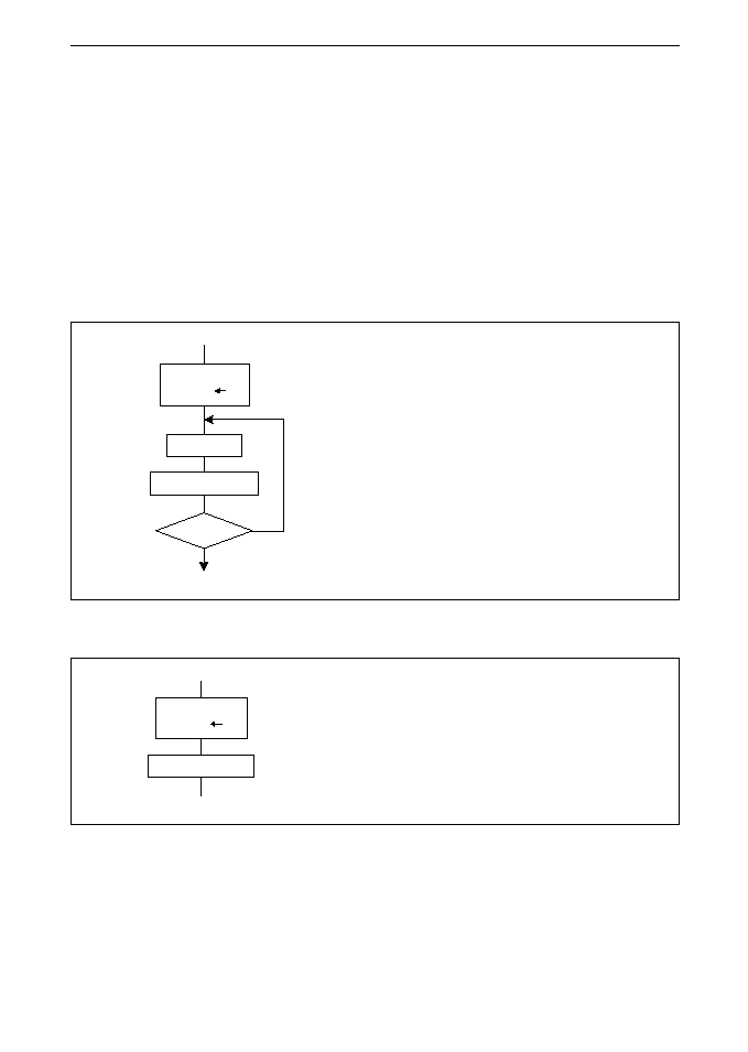
° Semiconductor
MSM6542-01/02/03
110
(b) ∑ R-D
1
to R-Y
10
when the CAL bit is 0
∑ C
D
, REST bit of C
E
, and C
F
(excluding the BANK 1/0 bit)
∑ A-S
1
to A-M
10
and A-W
∑ A-ENABLE and C
D
'
∑ C
E
' (excluding the DP bit)
There is no restriction other than by the DP bit.
(c) BANK 1/0
This bit can be rewritten freely even when the DP bit is 1.
(d) 30-s ADJ
Method 1
C
F
register
30-s ADJ 1
Idling
Is 30-s ADJ
bit 0 ?
Read C
F
register
Y
*
N
*At least about 100
Ķ
s
Method 2
Idling for 255 Ķs
C
F
register
30-s ADJ 1
*
* Maximum time required for 30sec adjustment under
assumption that oscillation is in progress
(e) DP
DP
1: Rewriting is possible 62
Ķ
s after the DP bit changes to 0.
DP
0: See "Temporarily canceling DP = 1 is a system for which DP is set at 1."
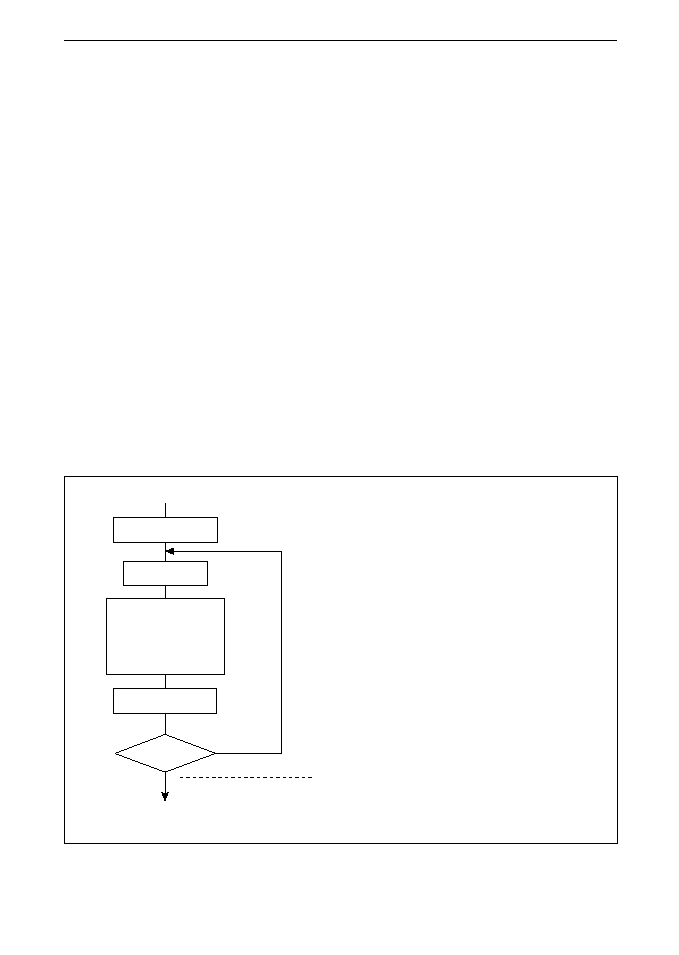
° Semiconductor
MSM6542-010/2/03
111
[Reading individual registers]
(a) Ordingary registers
Any registers can be read freely. However, the contents of the following bits change after
they are read.
∑ C
E
register
IRQ FLAG
1
:
When 1 is read from this bit with IT/PLS
1
set at 1, the bit is cleared
after read. For the timing when the bit is cleared, see the description
of the IRQ FLAG
1
bit of the C
E
register.
IRQ FLAG
2
:
When 1 is read from this bit with IT/PLS
2
set at 1, the bit is cleared
after read. For the timing when the bit is cleared, see the description
of the IRQ FLAG
2
bit of the C
E
register.
READ FLAG
:
When 1 is read from this bit, the bit is cleared after read.
TEST
1
, TEST
2
:
These bits are reset immediately when they are read. Therefore, 0
is always read from these bits.
(b) Reding time
Method 1 (unscheduled reading)
N
RF = 0
Read C
F
register
Read clock registers
* 2
* 1
* 3
Y
There is no carry while the clock registers
are being read.
Idling for 3 Ķs
Read C
F
register
*1
Dummy read to clear the READ FLAG (RF) bit
*2
Time required to increment the ripple counter
*3
Loop to retry read because of a carry generated in the
one-second digit counter during clock register reading
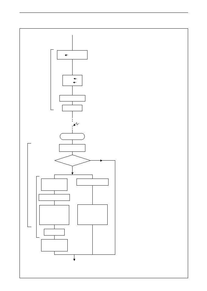
° Semiconductor
MSM6542-01/02/03
112
Method 2 (periodic readout)
C
D'
(0, d
2
, d
1
, d
0
)
* 2
IT/PLS
1
1
MASK
1
0
Read C
E
register
* 3
* 4
Idling
The CPU detects
an interrupt
Read C
E
register
IRQ FLAG
1
= 1
Y
When DP is 1
When DP is 0
Idling for at least 3 Ķs
Inhibit CPU from
accepting interrupts
Read clock registers
Read clock registers
Idling for at least 3 Ķs
* 5
* 5
Idling
* 6
Allow CPU to
accept interrupts
Other causes
* 7
* 8
N
* 1
Interrupt handling
routine
*5
Time required to increment the ripple
counter
*6, *7 The length of the time must be 122
Ķ
s
or more because interrupt output is
delayed 122
Ķ
s due to DP = 1. The
idling market *6 is provided for this
adjustment.
*8
To assure that readout is completed
before the next carry is generated, the
time required for these steps must
not be longer than the minimum set
time unit.
*1
Only for initial setting at power on
*2
The values of d2, d1, and d0 depend
on the required minimum time unit as
follows:
d2 d1 d0
When up to 1 s is required
1
0
1
When up to 1 min is required
1
1
0
When up to 10 min are required
1
1
1
*3
Dummy read to clear the IRQ FLAG
1
bit
*4
122
Ķ
s when the DP bit is 1,0
Ķ
s when
the DP bit is 0
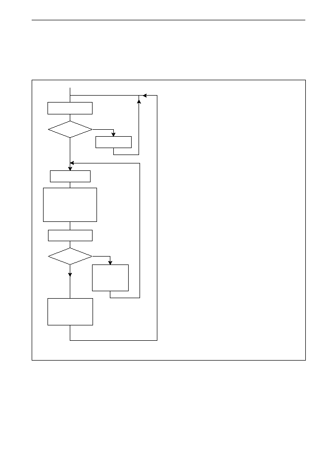
° Semiconductor
MSM6542-010/2/03
113
Method 3 (for each second carry)
(a) Setting (d2, d1, d0) at (1, 0, 1) in method 2 (periodical readout) described above
(b) Polling
Read C
F
register
RF = 1 ?
Idling
N
* 1
* 3
Idling for 3 Ķs
Read clock registers
Read C
F
register
RF = 0 ?
Discard read
data
Use read data
N
Y
* 2
Y
*1
Processing by other IC or wait time to prevent
unnecessary readouts which occur frequently.
A measure is 50 ms.
*2
Time required to increment the ripple counter
*3
Loop to retry read because of a carry generated
during clock register reading
° Semiconductor
MSM6542-01/02/03
114
[Setting for periodic pulse output]
Perform the following setting with the DP bit set at 0. The set values are independent of the
setting of the DP bit.
(a) Periodic pulse output (*1)
(b) Alarm pulse output (*1)
* 2
* 3
C
D
register
IT/PLS
1
0
MASK
1
1
C
E
register
IRQ 0
FLAG
1
Set C
D'
register
(*, CY
2
, CY
1
CY
0
)
C
D
register
IT/PLS
1
0
MASK
1
0
C
E
register
IRQ 0
FLAG
Idling for 185 Ķs
* 2
* 3
* 4
Set A-ENABLE register
(ae
8
, ae
4
, ae
2
, ae
1
)
Set A-S
1
to A-M
10
and A-W
C
D
register
IT/PLS
1
0
MASK
1
1
C
D
register
IT/PLS
2
0
MASK
2
0
*1
From the viewpoint of software, the IRQ FLAG
1
bit is used.
From the viewpoint of hardware, pin 1 (PERIODIC OUT)
is used for the MSM6542-3 or pin 1 (INTERRUP OUT) for
the MSM6542-1/2.
*2
For the MSM6542-1/2, a signal resulting from the ORing
with output triggered by an alarm is output to pin 1. When
alarm factors are not required, the MASK
2
bit must be set
at 1.
*3
The IRQ FLAG
1
bit is cleared.
*1
From the viewpoint of software, the IRQ FLAG
2
bit is used.
From the viewpoint of hardware, pin 2 (ALARM OUT) is
used for the MSM6542-3 or pin 1 (INTERRUPT OUT) for
the MSM6542-1/2.
*2
For the MSM6542-1/2, a signal resulting from the ORing
with output triggered by a periodic carry is output to pin
1. When periodic factors are not required, 1 must be set
in the MASK
1
bit.
*3
Time required to delete the previous output factors in the
IC.
*4
The IRQ FLAG
2
bit is cleared.
° Semiconductor
MSM6542-010/2/03
115
[Setting interrupt conditions]
Perfomr the following setting with the DP bit set at 0. The set values are independent of the
setting of the DP bit.
(a) Periodic interrupt output (*1)
(b) Alarm interrup output (*1)
* 2
* 3
C
D
register
IT/PLS
1
1
MASK
1
1
Set C
D'
register
(*, CY
2
, CY
1
,
CY
0
)
Dummy readout of C
E
register
C
D
register
IT/PLS
1
1
MASK
1
0
*1
From the viewpoint of software, the IRQ FLAG
1
bit is used. From the viewpoint of hardware, pin
1 (PERIODIC OUT) is used for the MSM6542-
03 or pin 1 (INTERRUPT OUT) for the MSM6542-
01/02.
*2
For the MSM6542-1/2, a signal resulting from
the ORing with output triggered by an alarm is
output to pin 1. When alarm factors are not
required, the MASK
2
bit must be set at 1.
*3
The IRQ FLAG
1
bit is cleared.
*1
From the viewpoint of software, the IRQ FLAG
2
bit is used. From the viewpoint of hardware, pin
3 (ALARM OUT) is used for the MSM6542-03
or pin 1 (INTERRUPT OUT) for the MSM6542-
01/02.
*2
For the MSM6542-01/02, a signal resulting
from the ORing with output triggered by a
periodic carry is output to pin 1. When periodic
factors are not required, 1 must be set in the
MASK
1
bit.
*3
Time required to output the previous interrupt
factors
*4
The IRQ FLAG
2
bit is cleared.
C
D
register
IT/PLS
2
1
MASK
2
1
Set A-S
1
to A-M
1O
and A-W
* 2
* 3
* 4
Idling for 185 Ķs
Set A-ENABLE register
Dummy readout of C
E
register
C
D
register
IT/PLS
2
1
MASK
2
0
° Semiconductor
MSM6542-01/02/03
116
[Sensing interrupts]
(a) When the DP bit is 0
Interrupt
Y
N
Another IC is
an interrupt
factor
Read C
E
register
Are both IRQ FLAG
1
and IRQ FLAG
2
bits
0 ?
Take action for
IRQ FLAG
1
and
IRQ FLAG
2
(b) When the DP bit is 1
Read C
E
register
ID on CPU side
Take action for IRQ
FLAG
1
and IRQ FLAG
2
Are both IRQ FLAG
1
and IRQ FLAG
2
bits
0 ?
IRQ FLAG
0
= 0
IE on CPU side
Another IC is
an interrupt
factor
Y
N
* 1
ID: Interrupt Disable
Y
N
* 2
N
Y
* 3
IE: Interrupt
Enable
Interrupt
Read C
E
register
Are both IRQ FLAG
1
and IRQ FLAG
2
bits
0 ?
Read C
E
register
*1
When the IRQ FLAG
1
and
IRQ FLAG
2
bits are read, they
are cleared. Restoration of
these pins to the open
output status is delayed up
to 122
Ķ
s. For this reason,
the CPU is interrupt-
disabled --- the CPU cannot
accept interrupts.
*2
When the maximum delay
of 122
Ķ
s described in *1
elapses, the IRA FLAG
0
bit
is set at 0.
*3
Since hardware output re-
questing an interrupt is re-
stored to the open status,
let the CPU interrupt enable.
° Semiconductor
MSM6542-010/2/03
117
[Basic check at the early stage of development]
(a) Read/write check
Only the BANK 1/0 bit can be subject to read and write operations without a paritcular
procedure.
The interface can be checked by reading and writing the BANK 1/0 bit.
Check D3 = 0
Read C
F
register
C
F
(0, 0, 0, 0)
R - S
1
(1, 1, 1, 1)
*1
*2
*3
Check D3 = 1
C
F
(1, 0, 0, 0)
A - S
1
(0, 1, 1, 1)
Read C
F
register
(b) Checking oscillation using software
Oscillator operation can be checked using software through increment of clock registers,
change of the IRQ FLAG
1
and IRQ FLAG
2
bits, 30-s adjustment, change of the read flag, and
setting the DP bit at 0. These methods, except setting the DP bit at 0, affect the REST and
STOP bits. Therefore, the method involved in the DP is used in the following flowcharts:
C
F
register
BANK 1/0 1
C
E'
register
DP 1
Read C
E'
register
DP 1
Y
N
*1
*2
1
*1
(D3, D2, D1, D0)
*2
Use addresses and data having values opposite
to those in *1 above to charge or discharge the
bus in the reverse phase.
*3
D3 is the BANK 1/0 bit.
*4
Same idea as *2
*1, *2
The DP bit is not set at 1 for 62
Ķ
s after it
changes from 1 to 0. When the step marked
*2 is executed within the 62
Ķ
s interval but
oscillation is in progress, the loop marked
*1 is completed within 62
Ķ
s.
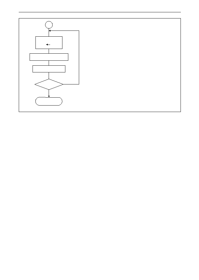
° Semiconductor
MSM6542-01/02/03
118
1
C
E'
register
DP 0
Idling for at least 11ms
*2
*3
Read C
E'
register
DP = 0 ?
Y
N
Oscillation is
in progress
*2
Time until the DP bit becomes 0 under as-
sumption that oscillation is in progress.
*3
The time required for this loop is prolonged by
the time equal to the one required to start
oscillation. Usually, this time is 0.5 to 2 s.
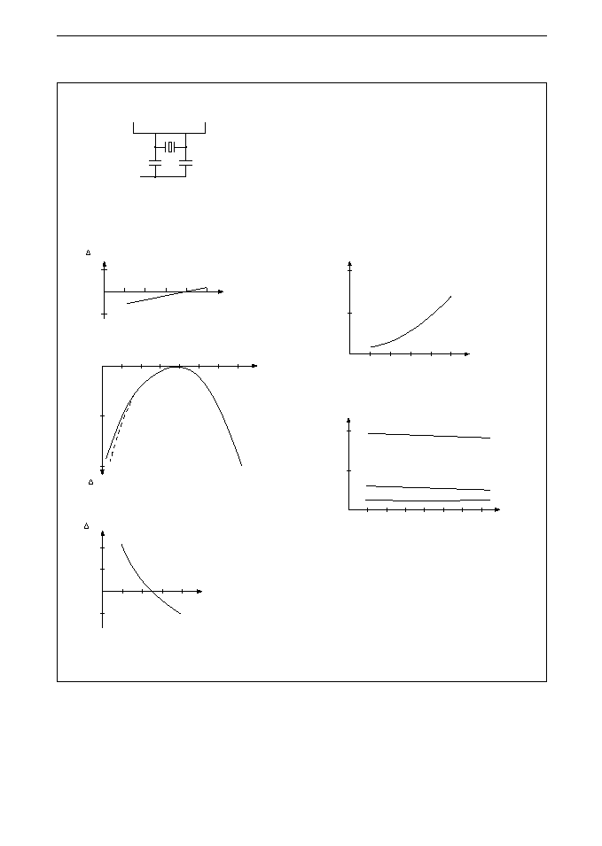
° Semiconductor
MSM6542-010/2/03
119
Reference experimental data
XT
XT
C
G
C
D
=32pF
C
G
=12pF
10
20
6
2
3
4
5
6
V
DD
(V)
Ta = 25įC
5
4
2
3
5
0
-5
80
/(PPM)
Ta(įC)
-40 -20
0
20
40
60
-100
-50
/
(PPM)
40
20
-20
5
10
15
20
-40
-20
40
20
80
60
10
5
I
DD
(ĶA)
0
Ta (įC)
I
DD
(ĶA)
o Dependency of oscillation frequency on power supply voltages
o Dependency of I
DD
on power supply voltages (Ta = 25įC)
o Dependency of oscillation frequency on temperatures
o Dependency of I
DD
on ambient temperatures
o Dependency of oscillation frequencies on capacitance
Note: The temperature characteristics of the capacitors used are class 0.
Crystral oscillator: P3 manufactured by Kinseki Co., Ltd.
(32.768 kHz)
Load capacity: CL=12pF
Equivalent series resistance: 30k
(MAX)
Secondary temperature coefficient of frequency
characteristics: -4.2 x 10
-8
/įC (MAX)
C
D
V
DD
V
DD
= 5V
V
DD
= 3V
V
DD
= 2V
V
DD
= 2V
V
DD
= 2V
C
D
= 32pF
V
DD
(V)
C
G
(pF)
/(PPM)
0
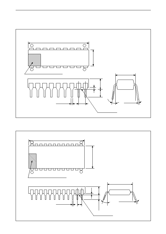
° Semiconductor
MSM6542-01/02/03
120
PACKAGE DIMENSIONS
18-pin plastic DIP
Seating Plane
1-pin index mark area
7.62 Ī0.30
0.6 MAX
0į~ 15į
2.54 Ī0.25
0.65 MAX
24.5 MAX
2.54 MIN
0.3 MAX
5.1 MAX
18
10
1
9
6.7 MAX
(Unit: mm)
24-pin plastic DIP
(Unit: mm)
1-pin index mark area
Seating Plane
14.2 MAX
15.24 Ī0.30
0.6 MAX
0į ~ 15į
2.54 Ī0.25
0.65 MAX
0.3 MIN
5.1 MAX
32.3 MAX
2.54 MIN
1
9
10
24
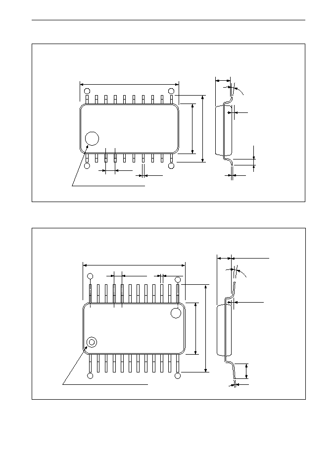
° Semiconductor
MSM6542-010/2/03
121
20-pin plastic flat
1-pin index mark area
0į ~ 10į
0.35
0.55 TYP
(Unit: mm)
0 ~ 0.3
0.15
1.6 Ī0.2
(Unit: mm)
1-pin index mark area (gloss)
1.27 Ī0.1
0.35 Ī0.1
2.2 Ī0.2
0.1 ~ 0.3
0į ~ 10į
0.2
1.0
7.9 Ī0.3
12.0 Ī0.4
1.6 Ī0.3
12
1
10
5.0 Ī0.3
6.8 Ī0.4
10.0 Ī0.3
20
11
0.95 Ī0.1
24
13
1
24-pin plastic flat