
1/23
° Semiconductor
MSM65512A/65P512A
GENERAL DESCRIPTION
The MSM65512A is a high-performance 8-bit microcontroller that employs OKI original nX-8/
50 CPU core. With a minimum instruction execution time of 400 ns (10MHz clock), the
MSM65512A is capable of high-speed processing, and includes 8K bytes of program memory,
256 bytes of data memory, timers and serial ports. Also available are the MSM65P512A, which
replaces the MSM65512's built-in program memory with one-time PROM, and the MSM65X512A,
which uses external program memory.
FEATURES
∑ Operating range
Operating frequency
: 0 to 10 MHz (V
DD
=4.5 to 5.5 V)
0 to 5 MHz (V
DD
=2.7 to 5.5 V)
Operating voltage
: 2.7 to 5.5 V
Operating temperature
: ≠40 to +85
∞
C (Operation at +125
∞
C is
assured by the other specification.)
∑ Memory space
: 64K bytes
Internal program memory
: 8K bytes
Internal data memory
: 256 bytes
∑ Minimum instruction execution time
: 400 ns @ 10 MHz
∑ Powerful instruction set
: 83 basic instructions
8/16-bit operation instructions
Bit manipulation instructions
Compound function instructions
∑ Abundant addressing modes
∑ Multiplication/division operation functions
: 8 • 8 ∆ 16
16/8 ∆ 16 ... 8
∑ I/O ports
Input-output port
: 4 ports • 8 bits
∑ Timers
: 8-bit auto-reload timer • 2
16-bit auto-reload timer • 1
Watchdog timer • 1
∑ Counters
: Time base counter • 1
16-bit free-running counter • 1
∑ Capture input
: 1 channel
∑ Compare output
: 2 channels
∑ Serial ports
: Shift register • 1
Serial port with baud rate generator
(UART/synchronous) • 1
∑ External interrupts
: 3
∑ Interrupt sources
: 15
∑ Package
40-pin plastic DIP (DIP40-P-600-2.54)
: (MSM65512A-•••RS,
MSM65P512A-•••RS)
44-pin plastic QFP (QFP44-P-910-0.80-2K)
: (MSM65512A-•••GS-2K,
MSM65P512A-xxxGS-2K)
44-pin plastic QFJ (PLCC) (QFJ44-P-S650-1.27): (MSM65512A-•••JS,
MSM65P512A-•••JS)
••• indicates the code number.
° Semiconductor
MSM65512A/65P512A
High Performance 8-Bit Microcontroller
E2E1011-27-Y4
This version: Jan. 1998
Previous version: Nov. 1996
2/23
° Semiconductor
MSM65512A/65P512A
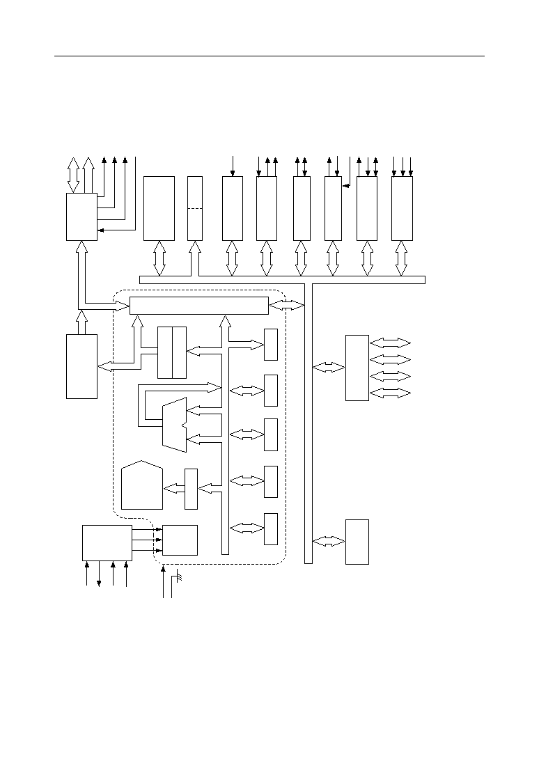
BLOCK DIAGRAM
OSC 0
OSC 1
RESET
HSTOP*
V
DD
GND
OSC
CONT.
ROM
(8K bytes)
EXT.MEM.
CONT.
CPU CORE
INST.
DEC.
T/C
IR
ALU
GMAR
PC
AR
BR
PSW
SP
LMAR
BUS
CONT.
I/O PORT
RAM
(256 bytes)
TBC
WDT
16-bit TIMER
16-bit FRC
CAP•1, CMP•2
SIO
AD0-7*
A8-15*
RD
WR*
ALE
EA
T2CK*
GATE*
CAP*
CMP0*
CMP1*
TXD*
RXD*
P0 P1 P2 P3
* Secondary functions of ports.
** One timer is used for the SIO
baud rate generator
8
8
8
8
8
8-bit TIMER•3**
T1OUT*
T0CK*
8-bit SHIFT-REG.
INTERRUPT CONT.
SFTO*
SFTI*
SFTCK*
INT0*
INT1*
INT2*
MUL/DIV
3/23
° Semiconductor
MSM65512A/65P512A
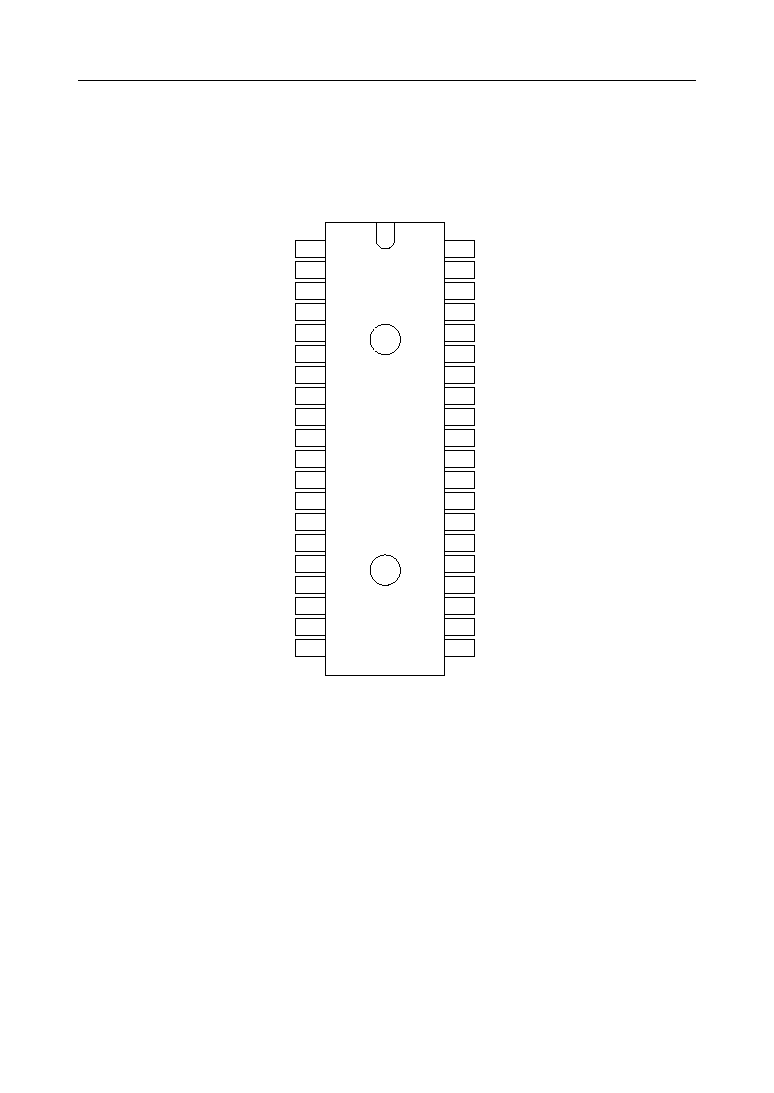
PIN CONFIGURATION (TOP VIEW)
40-Pin Plastic DIP
20
1
2
3
4
5
6
7
8
9
10
11
12
13
14
15
16
17
18
19
GND
P3.0/T2CK
P3.1/CAP
P3.2/CMP0
P3.3/CMP1
P3.4/INT2
P3.5/SFTO
P3.6/SFTI
P3.7/SFTCK
RESET
P2.0/RXD
P2.1/TXD
P2.2/INT0
P2.3/INT1/GATE
P2.4/T0CK
P2.5/HSTOP
P2.6/WR
P2.7/T1OUT
OSC1
OSC0
P1.0/A8
V
DD
P0.0/AD0
P0.1/AD1
P0.2/AD2
P0.3/AD3
P0.4/AD4
P0.5/AD5
P0.6/AD6
P0.7/AD7
EA
ALE
RD
P1.7/A15
P1.6/A14
P1.5/A13
P1.4/A12
P1.3/A11
P1.2/A10
P1.1/A9
21
40
39
38
37
36
35
34
33
32
31
30
29
28
27
26
25
24
23
22
4/23
° Semiconductor
MSM65512A/65P512A
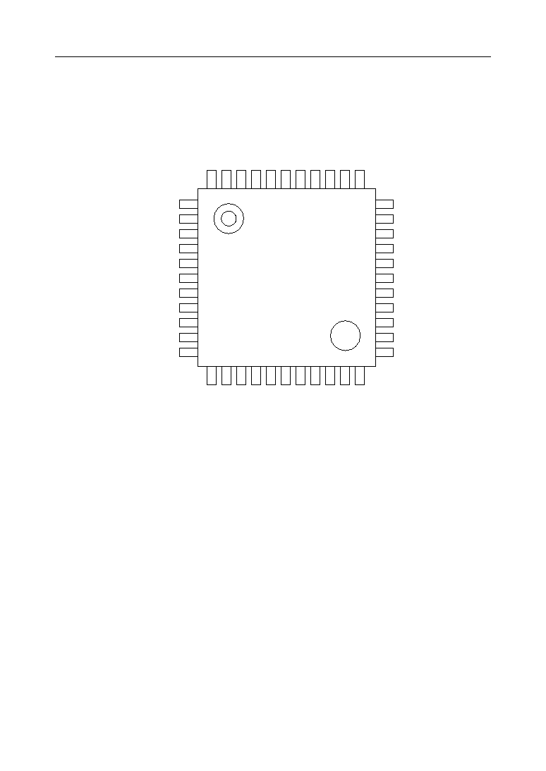
PIN CONFIGURATION (TOP VIEW) (Continued)
33
32
31
30
29
28
27
26
25
24
23
1
2
3
4
5
6
7
8
9
10
11
NC
P3.5/SFTO
P3.6/SFTI
P3.7/SFTCK
RESET
P2.0/RXD
P2.1/TXD
P2.2/INT0
P2.3/INT1/GATE
P2.4/T0CK
P2.5/HSTOP
P0.4/AD4
P0.5/AD5
P0.6/AD6
P0.7/AD7
EA
ALE
RD
P1.7/A15
P1.6/A14
P1.5/A13
NC
44
43
42
41
40
39
38
37
36
35
34
P3.4/INT2
P3.3/CMP1
P3.2/CMP0
P3.1/CAP
P3.0/T2CK
V
DD
P0.0/AD0
P0.1/AD1
P0.2/AD2
P0.3/AD3
NC
12
13
14
15
16
17
18
19
20
21
22
P2.6/
WR
P2.7/T1OUT
OSC1
OSC0
GND
*V
DD
P1.0/A8
P1.1/A9
P1.2/A10
P1.3/A11
P1.4/A12
* No-connection pin for MSM65P512A
NC: No-connection pin
44-Pin Plastic QFP
5/23
° Semiconductor
MSM65512A/65P512A
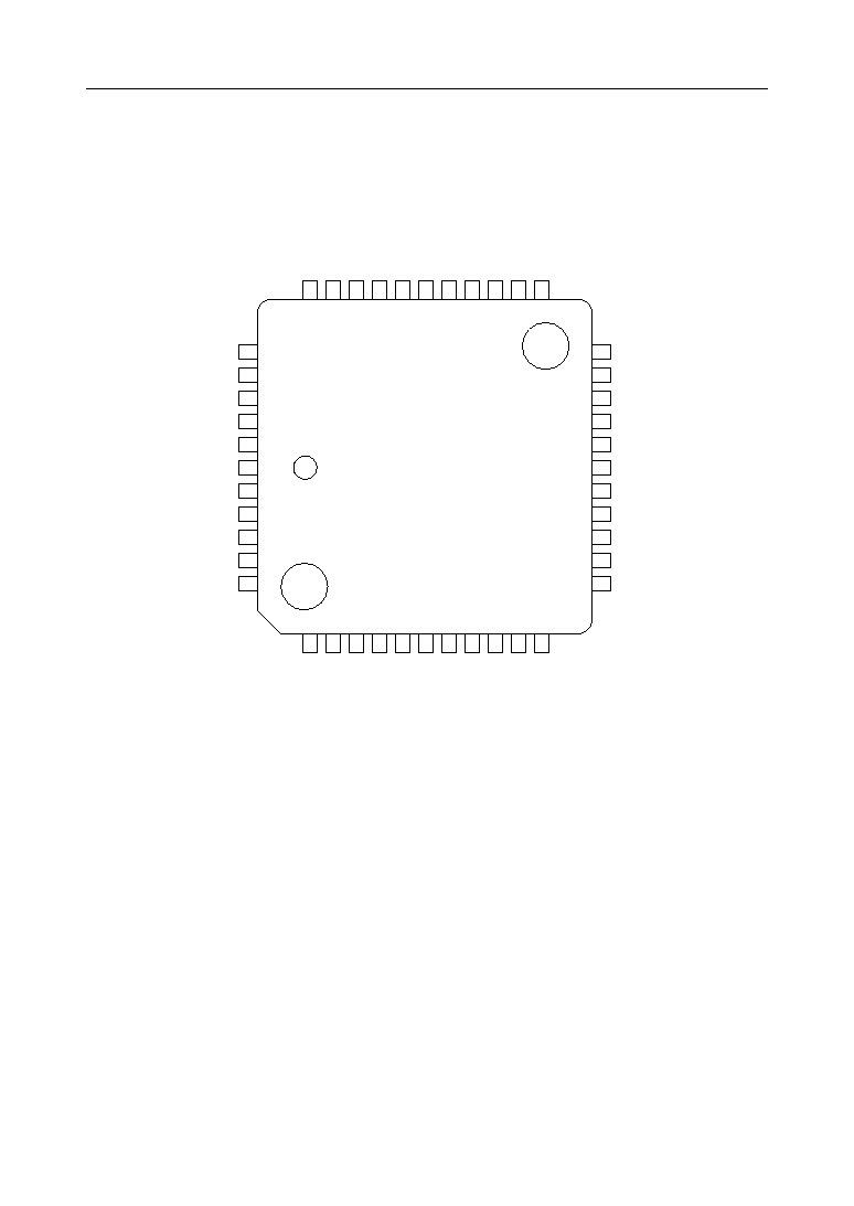
PIN CONFIGURATION (TOP VIEW) (Continued)
P0.3/AD3
P0.2/AD2
P0.1/AD1
P0.0/AD0
V
DD
P3.0/T2CK
P3.1/CAP
P3.2/CMP0
P3.3/CMP1
P3.4/INT2
NC
P1.4/A12
P1.3/A11
P1.2/A10
P1.1/A9
P1.0/A8
GND
OSC0
OSC1
P2.7/T1OUT
P2.6/WR
P3.5/SFTO
P3.6/SFTI
P3.7/SFTCK
RESET
P2.0/RXD
P2.1/TXD
P2.2/INT0
P2.3/INT1/GATE
P2.4/T0CK
P2.5/
HSTOP
P0.4/AD4
P0.5/AD5
P0.6/AD6
P0.7/AD7
EA
ALE
RD
P1.7/A15
P1.6/A14
P1.5/A13
NC
NC
NC
,
40
41
42
43
44
1
2
3
4
5
6
7
8
9
10
11
12
13
14
15
16
17
28
27
26
25
24
23
22
21
20
19
18
39
38
37
36
35
34
33
32
31
30
29
NC: No-connection pin
44-Pin Plastic QFJ (PLCC)
6/23
° Semiconductor
MSM65512A/65P512A
PIN DESCRIPTIONS
Basic Functions
Function
Symbol
Type
Description
Power
Supply
V
DD
+5V power supply
GND
0V digital ground
OSC0
Crystal oscillation input/external clock input
OSC1
Crystal oscillation output
I
O
RESET
System reset input (program starts from address 0040H);
internal pull-up resistor
I
EA
Program memory select input pin.
"L" level input for external program memory; "H" level input
for internal program memory.
I
RD
Read strobe signal during external memory access
O
ALE
Address latch signal during external memory access
O
PORT 0
8-bit Input-output port
During external memory access, becomes address/data bus for address
output, instruction fetch or data read/write along with ALE,
RD and WR pins
I/O
PORT 1
8-bit Input/output port
Address bus during external memory access
I/O
PORT 2
PORT 3
8-bit Input/output port • 2. Secondary functions shown in following table are
added for ports 2 and 3.
I/O
Oscillation
Control
Port
--
--

7/23
° Semiconductor
MSM65512A/65P512A
Secondary Functions
Symbol
Type
Description
INT0
P2.2 secondary function
External interrupt 0 input pin.
I
INT1/GATE
P2.3 secondary functions
External interrupt 1 input pin. Also used as input pin for gate signal
for timer 0 count enable/disable.
I
T0CK
P2.4 secondary function
Timer 0 external clock input pin.
I
HSTOP
P2.5 secondary function
Hard stop mode input pin; stops system clock oscillation with "L" level input.
I
WR
P2.6 secondary function
Write strobe signal output pin during external data memory access.
O
T1OUT
P2.7 secondary function
Output pin for signal obtained by dividing timer overflow by 2.
O
SFTO
P3.5 secondary function
Shift register data output pin.
O
SFTI
P3.6 secondary function
Shift register data input pin.
I
SFTCK
P3.7 secondary function
Shift register synchronizing clock input/output pin.
I/O
RXD
P2.0 secondary functions
UART: Input pin for serial port receive data.
Synchronous: Input/output pin for serial port transmit/receive data.
I/O
TXD
O
T2CK
P3.0 secondary function
Timer 2 external clock input pin.
I
CAP
P3.1 secondary function
Capture trigger input pin.
I
CMP0
P3.2 secondary function
Compare output channel 0 output pin.
O
CMP1
P3.3 secondary function
Compare output channel 1 output pin.
O
INT2
P3.4 secondary function
External interrupt 2 input pin
I
P2.1 secondary functions
UART: Output pin for serial port transmit data.
Synchronous: Output pin for serial port synchronizing clock.
8/23
° Semiconductor
MSM65512A/65P512A
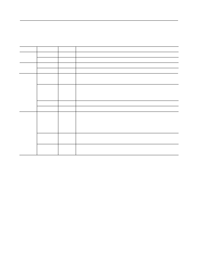
Port Circuit Configuration
Type
Port
Electrical Characteristics
(V
DD
=5V)
P0.0/AD0-
P0.7/AD7
1
"H" Input Voltage:
∑ V
IH
=2.4V
"L" Input Voltage:
∑ V
IL
=0.8V
"H" Output Voltage:
∑ V
OH
=3.75V
∑ I
OH
=≠400mA
"L" Output Voltage:
∑ V
OL
=0.4V
∑ I
OL
=3.2mA
Circuit Configuration
P1.0/A8-
P1.7/A15
2
"H" Input Voltage:
∑ V
IH
=2.4V
"L" Input Voltage:
∑ V
IL
=0.8V
"H" Output Voltage:
∑ V
OH
=3.75V
∑ I
OH
=≠200mA
"L" Output Voltage:
∑ V
OL
=0.4V
∑ I
OL
=1.6mA
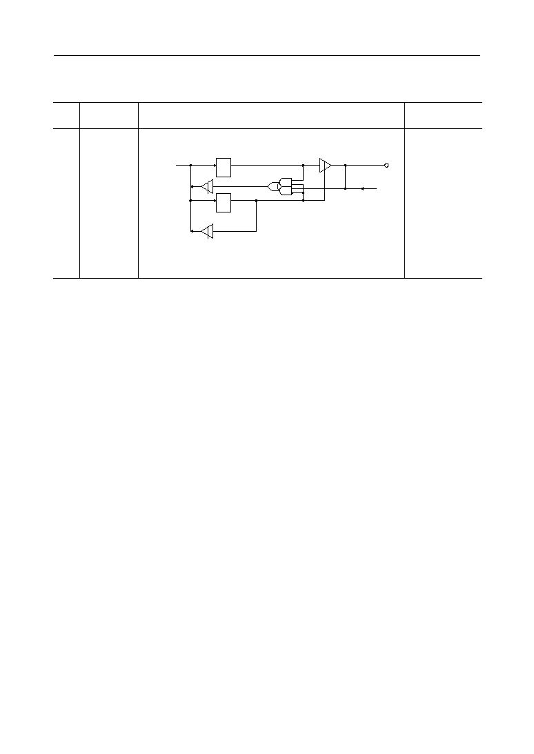
P0D
P0
DIR
Data Bus
External Memory Control
PORT0
P1D
P1
DIR
Data Bus
External Memory Control
PORT1
Data Bus
PxD
Px
DIR
Secondary
Output
Function
(x=2 to 5)
Px
MOD
PORTx
Secondary
Input
Function
3
"H" Input Voltage:
∑ V
IH
=2.4V
"L" Input Voltage:
∑ V
IL
=0.8V
P2.6/WR
"H" Output Voltage:
∑ V
OH
=3.75V
∑ I
OH
=≠400mA
"L" Output Voltage:
∑ V
OL
=0.4V
∑ I
OL
=3.2mA
Excluding P2.6/WR
"H" Output Voltage:
∑ V
OH
=3.75V
∑ I
OH
=≠200mA
"L" Output Voltage:
∑ V
OL
=0.4V
∑ I
OL
=1.6mA
P2.0/RXD,
P2.1/TXD,
P2.6/WR,
P2.7/T1OUT,
P3.2/CMP0,
P3.3/CMP1,
P3.5/SFT0,
P3.7/SFTCK
9/23
° Semiconductor
MSM65512A/65P512A
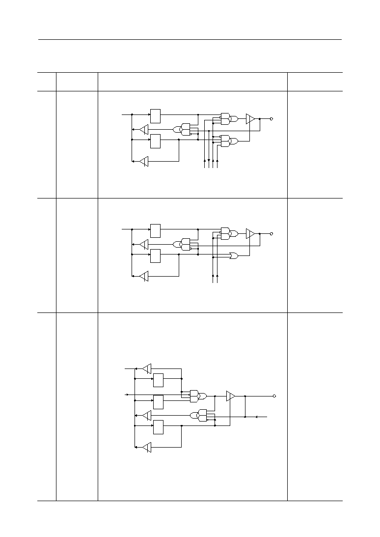
PxD
Px
DIR
Data Bus
(x=2 to 5)
PORTx
Secondary
Input Function
Type
Port
Electrical Characteristics
(V
DD
=5V)
4
"H" Input Voltage:
∑ V
IH
=2.4V
"L" Input Voltage:
∑ V
IL
=0.8V
"H" Output Voltage:
∑ V
OH
=3.75V
∑ I
OH
=≠200mA
"L" Output Voltage:
∑ V
OL
=0.4V
∑ I
OL
=1.6mA
Circuit Configuration
P2.2/INT0,
P2.3/INT1/GATE,
P2.4/T0CK,
P2.5/HSTOP,
P3.0/T2CK,
P3.1/CAP,
P3.4/INT2,
P3.6/SFTI
Port Circuit Configuration (Continued)

10/23
° Semiconductor
MSM65512A/65P512A
ABSOLUTE MAXIMUM RATINGS
RECOMMENDED OPERATING CONDITIONS
Parameter
Unit
Supply Voltage
V
DD
≠0.3 to 7.0
Symbol
Condition
Rating
Ta=25∞C
Input Voltage
V
I
≠0.3 to V
DD
+0.3
Output Voltage
V
O
≠0.3 to V
DD
+0.3
Power Dissipation
P
D
400
Ta=25∞C per package
50
Ta=25∞C per output
Storage Temperature
T
STG
≠55 to +150
--
V
mW
∞C
*1 This is due to the standard of a crystal oscillator or ceramic resonator.
MEMORY MAPS
100H
80H
40H
30H
20H
10H
0
0FFFFH
2000H
100H
80H
40H
20H
Internal Memory
Local Memory Space
SFR
Data Memory
Local Register Set 3
Local Register Set 2
Local Register Set 1
Local Register Set 0
General Memory Space
External Memory
Program Memory
Vector Call Table Area
Program Memory
Interrupt Vector Table Area
Vector Call Table Area
0
17FH
Data Memory
Page 1
Page 0
Parameter
Unit
Supply Voltage
V
DD
2.7 to 5.5
Symbol
Condition
Range
Refer to Figure 1.
Memory Hold Voltage
V
DDMH
2.0 to 5.5
f
OSC
=0 Hz
Oscillation Operating
Frequency *1
f
OSC
1 to 10
Refer to Figure 1.
External Clock Operating
Frequency
f
EXTCLK
0 to 10
Refer to Figure 1.
Operating Temperature
T
op
≠40 to +85
--
V
MHz
MHz
∞C
11/23
° Semiconductor
MSM65512A/65P512A
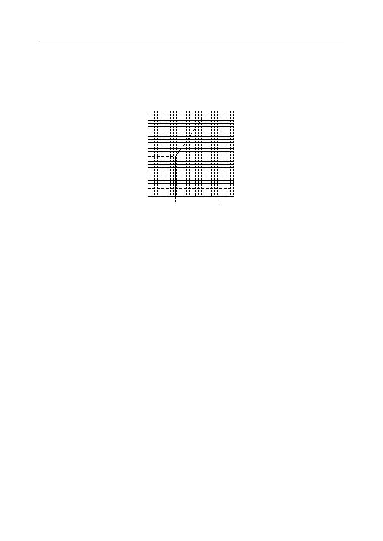
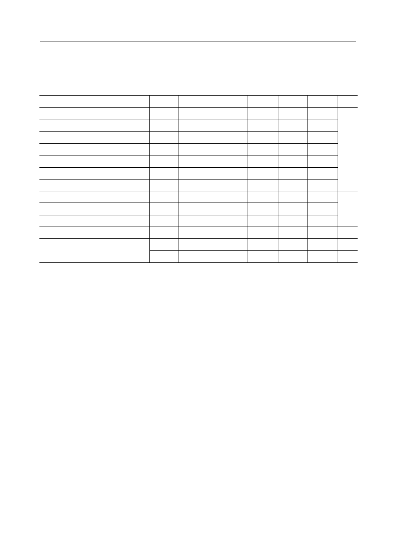
Figure 1. Operating Frequency vs. Power Supply Voltage
2
5
4
6
8
10
2
3
4
5
6
1
2.7
5.5
Ta=≠40 to +85∞C
f
OSC
, f
EXTCLK
(MHz)
* Oscillates at 1MHz or more.
V
DD
(V)
12/23
° Semiconductor
MSM65512A/65P512A
ELECTRICAL CHARACTERISTICS
DC Characteristics 1 (V
DD
=4.5 to 5.5V)
(GND=0V, Ta=≠40 to +85∞C)
Parameter
Symbol
Condition
Min.
Typ.
Max.
Unit
"H" Input Voltage 1
*1
V
IH1
--
2.4
--
V
DD
+0.3
"H" Input Voltage 2
*2
V
IH2
--
0.7V
DD
--
V
DD
+0.3
"L" Input Voltage
V
IL
--
≠0.3
--
0.8
"H" Output Voltage 1
*3
V
OH1
IOH=≠200mA
0.75V
DD
--
--
"H" Output Voltage 2
*4
V
OH2
IOH=≠400mA
0.75V
DD
--
--
"L" Output Voltage 1
*3
V
OL1
IOL=1.6mA
--
--
0.4
"L" Output Voltage 2
*4
V
OL2
IOL=3.2mA
--
--
0.4
Input Leakage Current 1
*5
I
LI1
VI=V
DD
/0V
--
--
±1
Input Leakage Current 2
*6
I
LI2
VI=V
DD
/0V
--
--
±10
"L" Input Current
*7
I
IL
VI=0V
≠40
≠200
≠400
Input Capacitance
C
I
f=1MHz, Ta=25∞C
--
5
--
Current Consumption
I
DDS
5V, Stop mode
*8
--
--
50
10MHz, 5V, no load
*9
V
mA
pF
mA
--
20
40
I
DDS
mA
*1 Excluding OSC0 and RESET
*2 OSC0 and RESET
*3 Excluding P0, ALE, RD, P2.6/WR
*4 P0, ALE, RD, P2.6/WR
*5 EA
*6 Excluding RESET, EA
*7 RESET
*8 The ports configured as inputs should be coupled to V
DD
or 0V. Other ports should not be
loaded.
*9 Refer to Figure 2.
13/23
° Semiconductor
MSM65512A/65P512A
DC Characteristics 2 (2.7
£ V
DD
<4.5V)
*1 Excluding OSC0 and RESET
*2 OSC0 and RESET
*3 Excluding P0, ALE, RD, P2.6/WR
*4 P0, ALE, RD, P2.6/WR
*5 EA
*6 Excluding RESET, EA
*7 RESET
*8 The ports configured as inputs should be coupled to V
DD
or 0V. Other ports should not be
loaded.
*9 Refer to Figure 2.
(GND=0V, Ta=≠40 to +85∞C)
Parameter
Symbol
Condition
Min.
Typ.
Max.
Unit
"H" Input Voltage 1
*1
V
IH1
--
0.5V
DD
+0.2
--
V
DD
+0.3
"H" Input Voltage 2
*2
V
IH2
--
0.6V
DD
+0.4
--
V
DD
+0.3
"L" Input Voltage
V
IL
--
≠0.3
--
0.15V
DD
+0.1
"H" Output Voltage 1
*3
V
OH1
I
OH
=≠10mA
0.75V
DD
--
--
"H" Output Voltage 2
*4
V
OH2
I
OH
=≠20mA
0.75V
DD
--
--
"L" Output Voltage 1
*3
V
OL1
I
OL
=10mA
--
--
0.1
"L" Output Voltage 2
*4
V
OL2
I
OL
=20mA
--
--
0.1
Input Leakage Current 1
*5
I
LI1
V
I
=V
DD
/0V
--
--
±1
Input Leakage Current 2
*6
I
LI2
V
I
=V
DD
/0V
--
--
±10
"L" Input Current
*7
I
IL
V
DD
=2.7 to 3.3V, V
I
=0V
≠40
≠120
≠240
Input Capacitance
C
I
f=1MHz, Ta=25∞C
--
5
--
Current Consumption
I
DDS
3V, Stop mode
*8
--
--
25
I
DD
5MHz, 3V, no load
*9
--
6
15
V
mA
pF
mA
mA
14/23
° Semiconductor
MSM65512A/65P512A
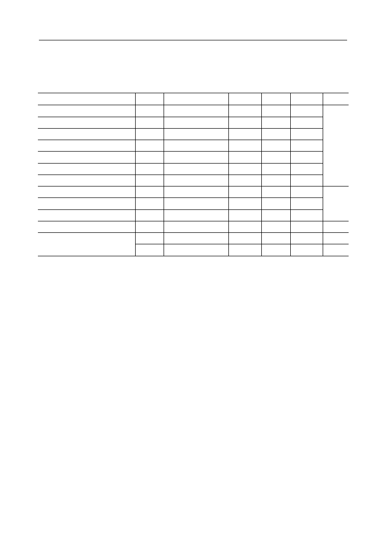
10
20
30
40
50
I
DD
(mA)
2
3
4
5
6
V
DD
(V)
10
20
30
40
50
I
DD
(mA)
2
3
4
5
6
V
DD
(V)
10
20
30
40
50
I
DD
(mA)
2
3
4
5
6
V
DD
(V)
10MHz
Max.
Typ.
Max.
Typ.
Max.
Typ.
6MHz
2MHz
Ta=≠40 to +85∞C, no load
Figure 2. Operating Current Consumption vs. Power Supply Voltage
15/23
° Semiconductor
MSM65512A/65P512A
AC Characteristics
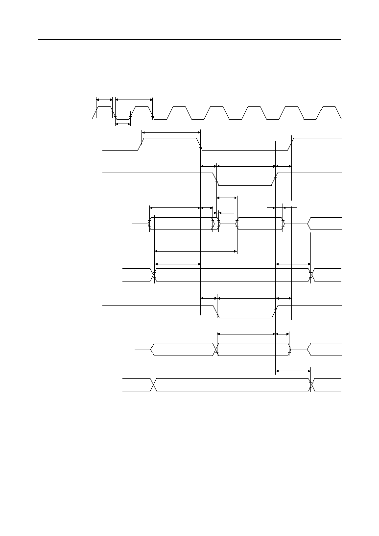
∑ External memory control
(V
DD
=2.7 to 5.5V, GND=0V, Ta=≠40 to +85∞C)
Parameter
Symbol
Condition
Min.
Max.
Unit
Clock Cycle
t
C
V
DD
=4.5 to 5.5V
100
--
"L" Clock Pulse Width
t
CLW
V
DD
=2.7 to 5.5V
45
--
"H" Clock Pulse Width
t
CHW
C
L
=100pF
45
--
Clock Cycle
t
C
200
--
"L" Clock Pulse Width
t
CLW
90
--
"H" Clock Pulse Width
t
CHW
90
--
ALE Pulse Width
t
AW
t
C
+t
CHW
≠20
--
ALE Pulse Delay Time 1
t
ALD1
t
CLW
≠20
--
ALE Pulse Delay Time 2
t
ALD2
t
CLW
≠20
--
RD Pulse Width
t
RW
t
C
+t
CHW
≠40
--
RD Pulse Delay Time
t
RD
t
CLW
≠40
t
CLW
+20
WR Pulse Width
t
WW
t
C
+t
CHW
≠40
--
WR Pulse Delay Time
t
WD
t
CLW
≠20
t
CLW
+40
"L" Address Setup Time
t
LAS
t
C
≠40
--
"H" Address Setup Time
t
HAS
t
C
≠40
--
"L" Address Hold Time
t
LAH
t
CLW
≠20
--
Bus Float Time
t
LAZ
--
20
"H" Address Hold Time
t
HAHR
t
C
≠20
--
"H" Address Hold Time
t
HAHW
t
C
≠20
--
Read Data Access Time
t
RDAA
--
t
C
+t
CLW
≠15
Read Data Access Time
t
RDAR
--
t
CHW
+10
Read Data Hold Time
t
RDH
0
--
Write Data Setup Time
t
WDS
t
C
+t
CLH
≠40
--
Write Data Hold Time
t
WDH
t
CLW
≠20
--
ns
16/23
° Semiconductor
MSM65512A/65P512A
OSC0
t
CHW
t
C
t
AW
t
CLW
t
RD
t
RDAR
t
LAS
t
LAZ
t
RDAA
t
HAS
t
WD
t
WDS
t
HAHW
t
RW
t
ALD1
t
LAH
t
RDH
t
HAHR
t
WW
t
ALD2
t
WDH
ADDRESS L
INST or
DATA IN
ADDRESS H
ADDRESS L
DATA OUT
ADDRESS H
ALE
RD
P0
P1
WR
P0
P1
17/23
° Semiconductor
MSM65512A/65P512A
∑ CPU control
*1 Excluding power ON, stop mode and hard stop mode.
*2 During power ON, in stop mode and hard stop mode.
*3 Oscillation stabilization time depends on resonator.
(V
DD
=2.7 to 5.5V, GND=0V, Ta=≠40 to +85∞C)
Parameter
Symbol
Condition
Min.
Max.
Unit
RESET Pulse Width *
1
t
RESW1
20
--
--
ns
RESET Pulse Width *
2
t
RESW2
*
3
--
--
--
RESET pulse width
t
RESW1
,
2
RESET
∑ Peripheral control 1
* t
T0CLK
: Timer 0 count clock cycle selected by T0CON.
(V
DD
=2.7 to 5.5V, GND=0V, Ta=≠40 to +85∞C)
Parameter
Symbol
Condition
Min.
Max.
Unit
Clock Cycle
t
C
100
--
ns
External Interrupt Pulse
Width
t
EXIW
4 t
C
--
External Clock Pulse
Width
t
T0CW
4 t
C
--
GATE Pulse Width
t
T0GW
1 t
TOCLK
*
--
--
OSC
EXI
T0
External Clock Pulse
Width
t
T2CW
4 t
C
--
T2
CAP Pulse Width
t
CAPW
12 t
C
--
CAP
V
DD
=4.5 to 5.5V
200
--
V
DD
=2.7 to 5.5V
18/23
° Semiconductor
MSM65512A/65P512A
1) EXI pulse width
2) T0
3) T2
4) CAP
OSC0
t
C
t
CLW
T0CK
t
T0CW
GATE
t
T0GW
T2CK
t
T2CW
CAP
t
CAPW
INT0-2
t
EXIW
19/23
° Semiconductor
MSM65512A/65P512A
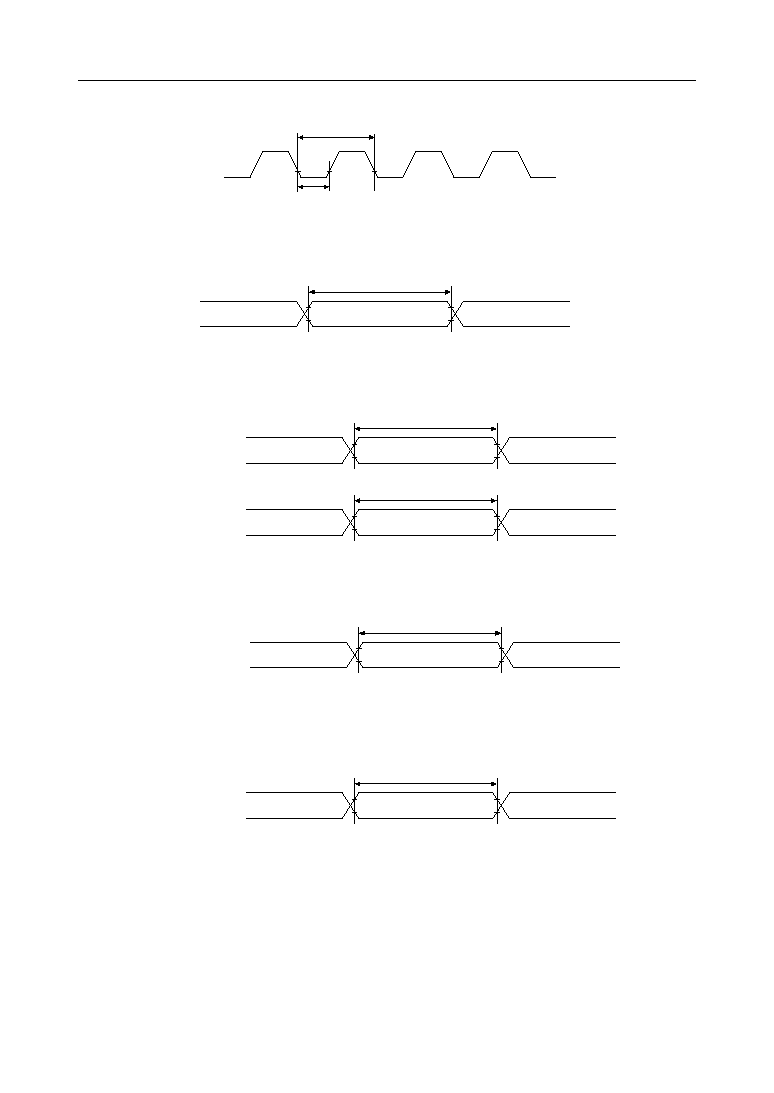
∑ Peripheral control 2
(V
DD
=2.7 to 5.5V, GND=0V, Ta=≠40 to +85∞C)
Parameter
Symbol
Condition
Min.
Max.
Unit
Clock Cycle
t
C
100
--
ns
SFTCK Cycle
t
SFC
8 t
C
--
SFTCK "L" Pulse Width
t
SFCLW
4 t
C
≠20
--
SFTCK "H" Pulse Width
t
SFCHW
4 t
C
≠20
--
OSC
SFT
SFTCK Setup Time
t
SFOS
t
SFCLW
≠100
--
SFTO Hold Time
t
SFOH
t
SFCHW
≠100
--
SFTI Setup Time
t
SFIS
100
--
SFTI Hold Time
t
SFIH
100
--
C
L
=100pF
Synchronous Clock Cycle
t
SIC
8 t
C
--
Synchronous Clock "L"
Pulse Width
t
SICLW
4 t
C
≠20
--
Synchronous Clock "H"
Pulse Width
t
SICHW
4 t
C
≠20
--
Output Data Setup Time
t
SIOS
6 t
C
≠100
--
Output Data Hold Time
t
SIOH
2 t
C
≠100
--
Input Data Setup Time
t
SIIS
t
C
+t
CLW
+100
--
Input Data Hold Time
t
SIIH
0
--
SIO
(Clock
Syn-
chro-
nous)
V
DD
=4.5 to 5.5V
200
--
V
DD
=2.7 to 5.5V
20/23
° Semiconductor
MSM65512A/65P512A
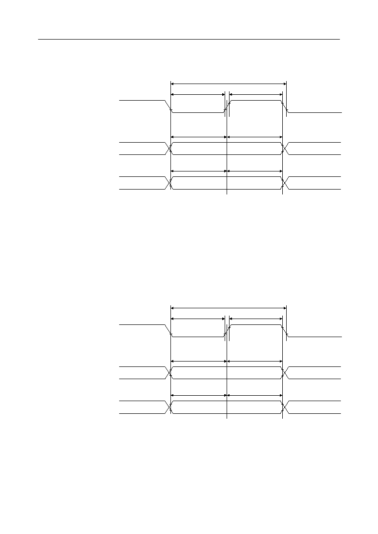
1) SFT
2) SIO
(Clock synchronous mode)
t
SFCLW
t
SFCHW
t
SFC
t
SFOS
t
SFOH
t
SFIS
t
SFIH
SFTCK
SFTO
SFTI
t
SICLW
t
SICHW
t
SIC
t
SIOS
t
SIOH
t
SIIS
t
SIIH
TXD
RXD (transmission)
RXD (reception)
21/23
° Semiconductor
MSM65512A/65P512A
(Unit : mm)
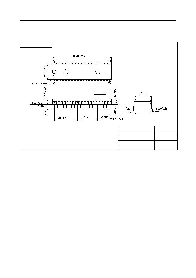
PACKAGE DIMENSIONS
Notes for Mounting the Surface Mount Type Package
The SOP, QFP, TSOP, SOJ, QFJ (PLCC), SHP and BGA are surface mount type packages, which
are very susceptible to heat in reflow mounting and humidity absorbed in storage.
Therefore, before you perform reflow mounting, contact Oki's responsible sales person for the
product name, package name, pin number, package code and desired mounting conditions
(reflow method, temperature and times).
DIP40-P-600-2.54
Package material
Lead frame material
Pin treatment
Solder plate thickness
Package weight (g)
Epoxy resin
42 alloy
Solder plating
5 mm or more
6.10 TYP.
22/23
° Semiconductor
MSM65512A/65P512A
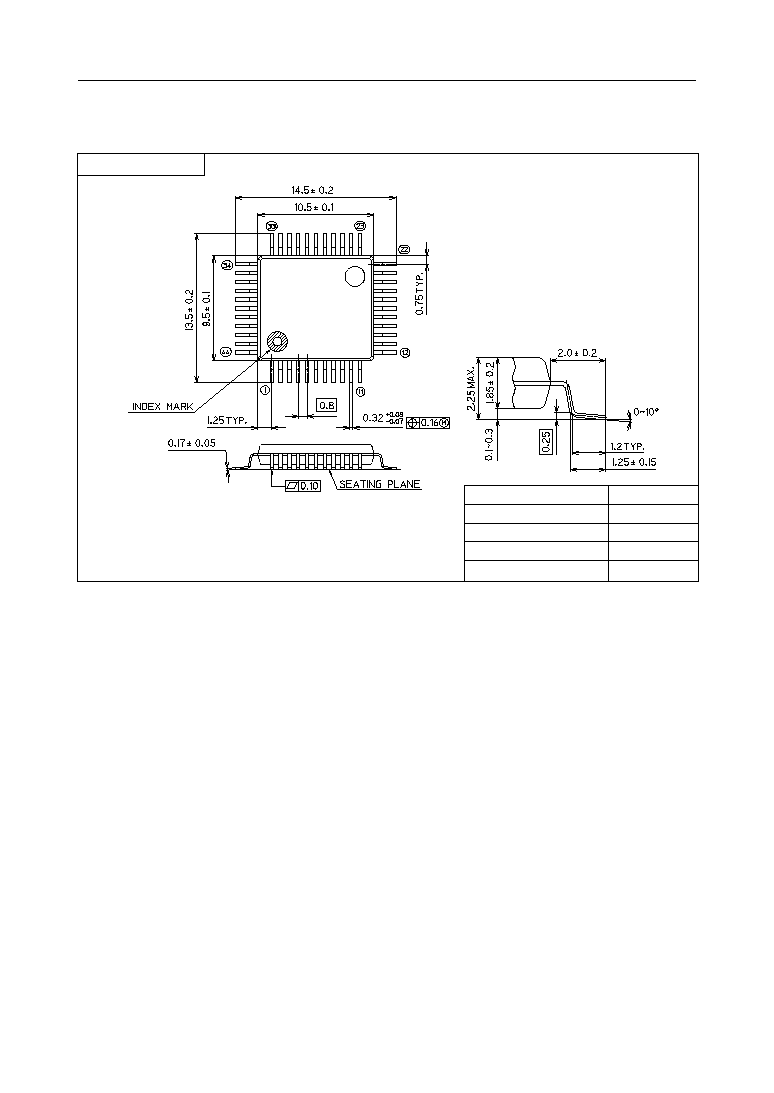
(Unit : mm)
Notes for Mounting the Surface Mount Type Package
The SOP, QFP, TSOP, SOJ, QFJ (PLCC), SHP and BGA are surface mount type packages, which
are very susceptible to heat in reflow mounting and humidity absorbed in storage.
Therefore, before you perform reflow mounting, contact Oki's responsible sales person for the
product name, package name, pin number, package code and desired mounting conditions
(reflow method, temperature and times).
Package material
Lead frame material
Pin treatment
Solder plate thickness
Package weight (g)
Epoxy resin
42 alloy
Solder plating
5 mm or more
0.41 TYP.
QFP44-P-910-0.80-2K
Mirror finish
23/23
° Semiconductor
MSM65512A/65P512A
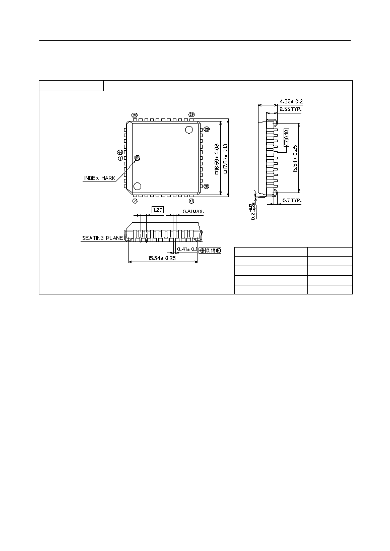
(Unit : mm)
Notes for Mounting the Surface Mount Type Package
The SOP, QFP, TSOP, SOJ, QFJ (PLCC), SHP and BGA are surface mount type packages, which
are very susceptible to heat in reflow mounting and humidity absorbed in storage.
Therefore, before you perform reflow mounting, contact Oki's responsible sales person for the
product name, package name, pin number, package code and desired mounting conditions
(reflow method, temperature and times).
QFJ44-P-S650-1.27
Package material
Lead frame material
Pin treatment
Solder plate thickness
Package weight (g)
Epoxy resin
Cu alloy
Solder plating
5 mm or more
2.00 TYP.
Mirror finish