 | –≠–ª–µ–∫—Ç—Ä–æ–Ω–Ω—ã–π –∫–æ–º–ø–æ–Ω–µ–Ω—Ç: MSM6569 | –°–∫–∞—á–∞—Ç—å:  PDF PDF  ZIP ZIP |
s
s
≠≠≠≠≠≠≠≠≠≠≠≠≠≠≠≠≠≠≠≠≠≠≠≠≠≠≠≠≠≠≠≠≠≠≠≠≠≠≠≠≠≠≠≠≠≠≠≠≠≠≠≠≠≠≠≠≠≠≠≠≠≠≠≠≠≠≠≠≠≠≠≠≠≠≠≠≠≠≠≠≠≠≠≠≠≠≠≠≠
1
OKI SEMICONDUCTOR
INTRODUCTION
With the continuing demand for smaller and more efficient systems, designers are seeking new ways to reduce power
and increase integration. This paper describes how good use of OKI Semiconductor's monolithic display drivers can
reduce power consumption and component count in systems that incorporate liquid crystal displays (LCDs). Infor-
mation in this paper is applicable both to small LCD panels (with a dozen or less segmented digits) and to large LCD
panels (such as used for laptop screens).
LCD elements are capacitive in nature and dissipate virtually no power, whether selected or deselected. When an
LCD element is selected, a voltage is applied across the liquid crystal that varies the element's reflectivity. Removing
the voltage deselects the LCD element and returns the liquid crystal to its original state.
In general, an alternating-current (AC) source is required to illuminate the individual elements in an LCD panel. A
direct-current (DC) source is not suitable for driving an LCD panel because of electrolytic reactions in the LCD's
liquid. Placing a potential difference across the liquid in an LCD panel causes ion migration, which gradually erodes
the anode terminal and causes destructive deposition on the cathode terminal. The electrolytic reaction could be
diminished by plating the electrodes with a non-reactive conductive element, such as gold, for example; however,
the high cost of gold and similar non-reactive elements makes this solution impractical for all but the most esoteric
applications.
A far simpler way to eliminate electrolytic corrosion is to use an AC source to drive the LCD panel, eliminating uni-
directional ion migration and the associated problems. AC configurations for driving LCDs fall in two main catego-
ries, which are:
∑
Static driver configurations
∑
Multiplexed driver configurations
The next two sections describe these two configurations. The third section in this application note addresses power-
related issues. This application note concludes with some complete circuit examples.
USING STATIC DRIVERS
In configurations using static drivers, a separate driver signal (SEG) provides an AC source for each element, and all
elements use a single shared common (COM) terminal.
LCD elements are often
segments
of an alphanumeric digit. In larger configurations, LCD elements are individual
dots
that emulate the appearance of a CRT monitor. Static driver configurations are simple to use and are generally
suitable for LCDs with less than 80 segments.
OKI Semiconductor supplies a range of single-chip solutions for static LCD driver configurations, some of which
also include built-in RC oscillation circuits, in small-outline IC (SOIC) and plastic quad flat pack (PQFP) packages.
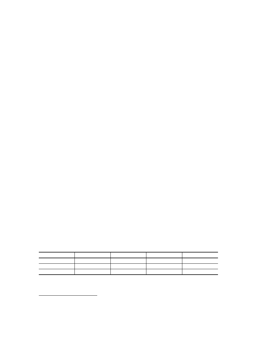
The table below lists the main characteristics of single-chip static LCD drivers from OKI Semiconductor.
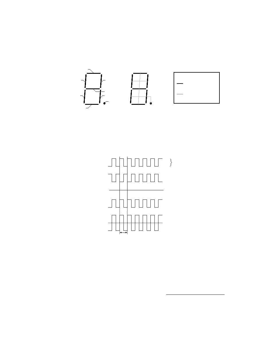
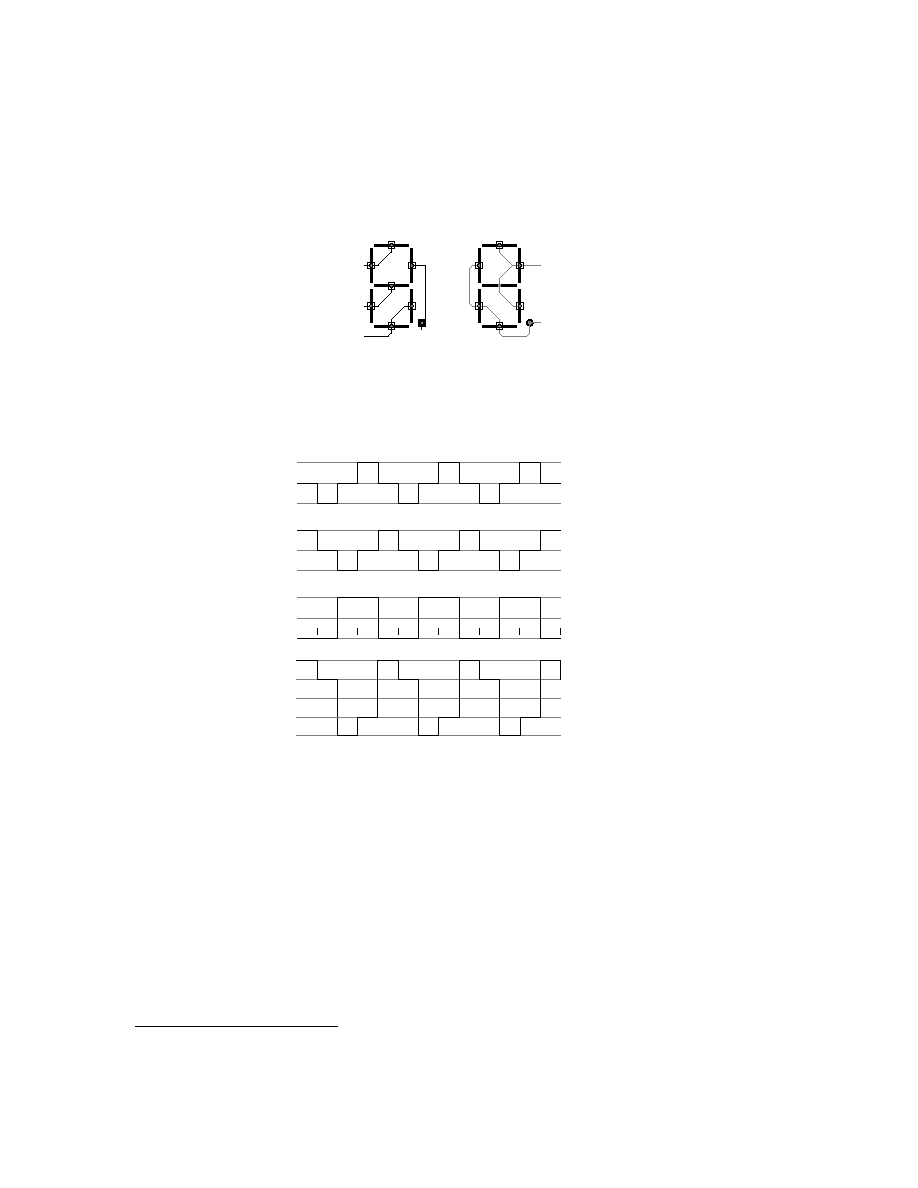
Figure 1
below shows static driver connections to a single-digit, seven-segment alphanumeric display. Separate driv-
ers, SEG1 - SEG8, power each segment. All segments share a common ground connection, COM.
LCD Drivers for Static Configurations
Part Number
Segments
On-Chip Oscillator
Drive Voltage (V
LCD
)
Package
MSM5219B
48
4.0 - 7.0
60-lead PQFP
MSM5221
56
X
3.0 - 7.0
80-lead PQFP
MSM5265
80
3.0 - 6.0
100-lead PQFP
≠≠≠≠≠≠≠≠≠≠≠≠≠≠≠≠≠≠≠≠≠≠≠≠≠≠≠≠≠≠≠≠≠≠≠≠≠≠≠≠≠≠≠≠≠≠≠≠≠≠≠≠≠≠≠≠≠≠≠≠≠≠≠≠≠≠≠≠≠≠≠≠≠≠≠≠≠≠≠≠≠≠≠≠≠≠≠≠
s
s
2
OKI SEMICONDUCTOR
Figure 2
below shows the AC waveforms for driving the illustrated display. When an element is deselected, the com-
bined COM and SEG signals negate each other, as shown for the (COM ≠ SEG1) signal illustrated below. When an
element is selected, the combined COM and SEG signals constructively reinforce each other, as shown for the (COM
≠ SEG2) signal below.
In static drive configurations, the AC frequency used to drive each segment is identical. This AC frequency is called
the
frame frequency
. In static drive configurations, a single element is selected or deselected in any one individual
frame, as shown in
Figure 2
above.
Static driver configurations generally use a frame frequency in the 20-200 Hz range. Lower frame frequencies can
cause visible flicker. Higher frame frequencies do not provide sufficient time for charging the capacitive LCD ele-
ments.
SEG7
SEG6
SEG1
SEG2
SEG3
SEG5
SEG4
SEG8
Figure 1. Segment Connections for Static-Drive Configurations
COM
Segment connections over
the liquid crystal.
KEY:
Common base connections
under the liquid crystal.
Figure 2. Functional Waveforms for Static Drive Configurations
COM
SEG1
SEG2
COM ≠ SEG2
V
DD
V
L
V
DD
V
L
V
DD
V
L
V
LCD
-V
LCD
0V
COM ≠ SEG1
(Selected)
(Deselected)
0V
V
LCD
1 Frame
(Deselected)
(Selected)
s
s
≠≠≠≠≠≠≠≠≠≠≠≠≠≠≠≠≠≠≠≠≠≠≠≠≠≠≠≠≠≠≠≠≠≠≠≠≠≠≠≠≠≠≠≠≠≠≠≠≠≠≠≠≠≠≠≠≠≠≠≠≠≠≠≠≠≠≠≠≠≠≠≠≠≠≠≠≠≠≠≠≠≠≠≠≠≠≠≠≠
3
OKI SEMICONDUCTOR
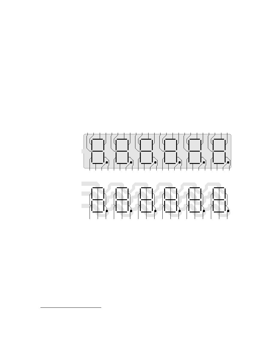
USING MULTIPLEXED DRIVERS
For configurations requiring more than about 80 drivers, it is more efficient to multiplex the COM and SEG signals
than to use a static driver configuration. In multiplexed configurations, each SEG driver signal powers more than one
segment, and the circuit uses more than one COM signal. The SEG and COM signals actually form a grid, with each
segment driven by a unique SEG/COM node. The multiplexed drive method reduces the number of driver circuits
and the number of connections between the circuit and the display cell. This reduces cost when driving many display
elements.
Figure 1
below illustrates this reduction in driver count by comparing static and multiplexed drive configurations for
a six-digit display. The static driver configuration requires 49 connections to the LCD, whereas the multiplexed con-
figuration requires only 21 connections. Increasing the degree of multiplexing can further reduce the number of con-
nections; however, increased multiplexing also reduces the circuit's tolerance to voltage variation.
A range of multiplexed configurations are possible, distinguished by:-
∑
Bias
, indicating the number of voltage levels used to power the LCD display.
∑
Duty Cycle
, indicating the number of segments driven by each individual output driver.
∑
Frame Frequency Type,
indicating whether the COM signal alternates over one frame (Type A) or two frames
(Type B).
For example, in a 1/2 bias, 1/2 duty-cycle configuration, each individual output driver uses two voltage levels to drive
two segments. Similarly, in a 1/3 bias, 1/3 duty-cycle configuration, each driver uses three voltage levels to drive
three segments (
Figure 1
above is a 1/3 bias, 1/3 duty cycle configuration).
Frame frequency determines the degree of flickering and vividness. For a high degree of multiplexing, the type-B
configuration can make the display more vivid, but can also introduce flickering at lower clock frequencies.
Figure 4
1
A
ComA
ComB
ComC
Common
Static
Multiplex
1/3 bias,
1/3 duty cycle
2
A
3
A
4
A
5
A
7
A
6
A
8
A
1
B
2
B
3
B
4
B
5
B
7
B
6
B
8
B
1
C
2
C
3
C
4
C
5
C
7
C
6
C
8
C
1
D
2
D
3
D
4
D
5
D
7
D
6
D
8
D
1
E
2
E
3
E
4
E
5
E
7
E
6
E
8
E
1
F
2
F
3
F
4
F
5
F
7
F
6
F
8
F
S
3
S
1
S
2
S
6
S
4
S
5
S
9
S
7
S
8
S
10
S
11
S
12
S
13
S
14
S
15
S
16
S
17
S
18
Figure 3. Static versus Multiplexed Configurations
≠≠≠≠≠≠≠≠≠≠≠≠≠≠≠≠≠≠≠≠≠≠≠≠≠≠≠≠≠≠≠≠≠≠≠≠≠≠≠≠≠≠≠≠≠≠≠≠≠≠≠≠≠≠≠≠≠≠≠≠≠≠≠≠≠≠≠≠≠≠≠≠≠≠≠≠≠≠≠≠≠≠≠≠≠≠≠≠
s
s
4
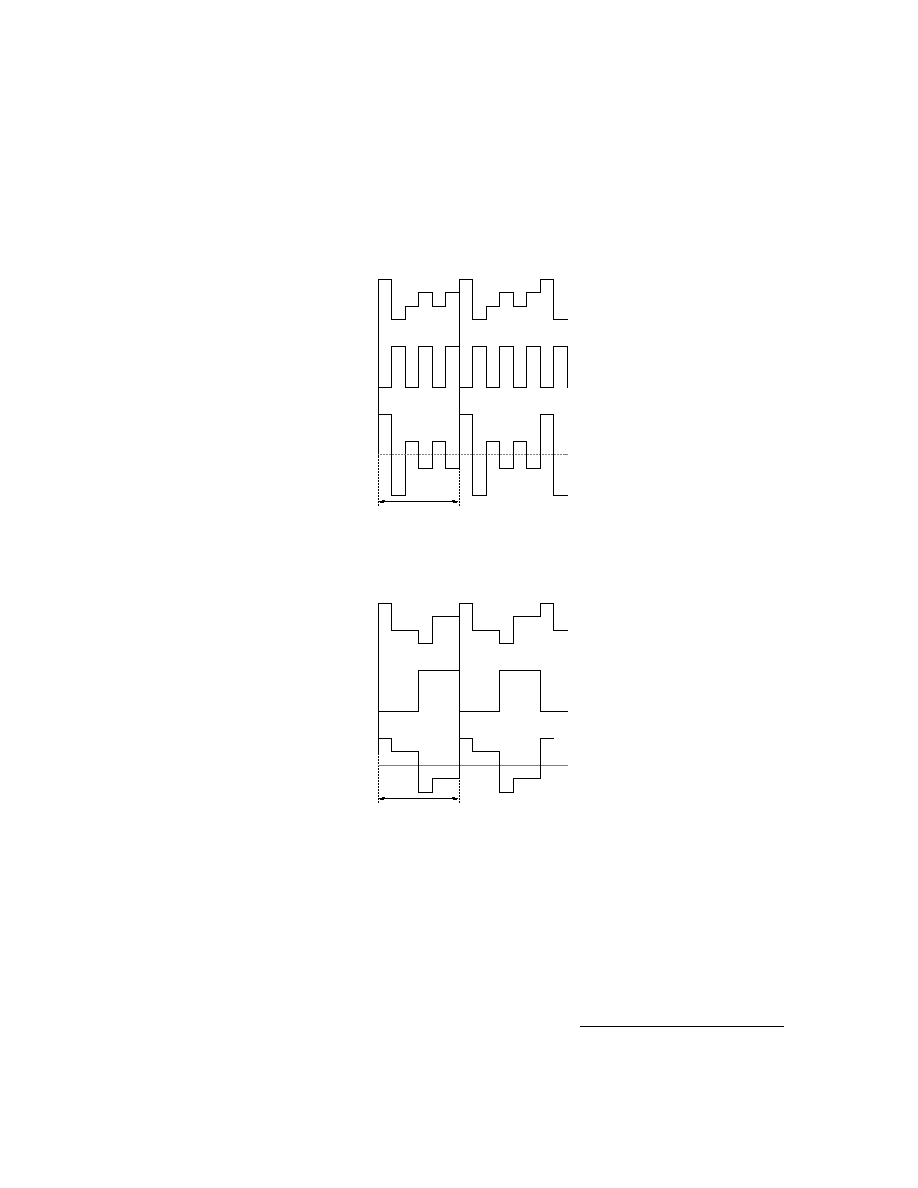
OKI SEMICONDUCTOR
and
Figure 5
below illustrate the difference between type-A and type-B configurations for the LCD driver network
shown in
Figure 1
above.
Type B configurations are more common, as the maximum required frequency is lower.
Figure 6
through
Figure 10
illustrate various multiplexed configuration, all of which use a Type B configuration to reduce frame frequency.
Figure 6
on the next page illustrates how a 1/2 bias, 1/2 duty cycle, Type B configuration can drive 62 outputs. This
particular example is suitable for systems using the MSM6660. Full V
LCD
voltage is applied across the selected seg-
ment for display and less than full V
LCD
voltage is applied across the deselected segment.
COM
SEG
COM ≠ SEG
1 Frame
Figure 4. A-Type Waveforms for a 1/3 Duty Cycle, 1/3 Bias Configuration
SEG
COM ≠ SEG
1 Frame
Figure 5. B-Type Waveforms for a 1/3 Duty Cycle, 1/3 Bias Configuration
COM
s
s
≠≠≠≠≠≠≠≠≠≠≠≠≠≠≠≠≠≠≠≠≠≠≠≠≠≠≠≠≠≠≠≠≠≠≠≠≠≠≠≠≠≠≠≠≠≠≠≠≠≠≠≠≠≠≠≠≠≠≠≠≠≠≠≠≠≠≠≠≠≠≠≠≠≠≠≠≠≠≠≠≠≠≠≠≠≠≠≠≠
5
OKI SEMICONDUCTOR
Figure 7
below shows the waveforms for the 1/2 bias, 1/2 duty cycle configuration shown in
Figure 6
above.
Figure 8
illustrates a 1/3 bias, 1/3 duty cycle, Type B LCD network, suitable for connection to OKI's MSM6606.
SEG1
SEG2
SEG3
SEG4
COMA
COMB
Figure 6. A 1/2 Bias, 1/2 Duty Cycle, Type B Configuration
COM1
V
LC1
,
2
V
DD
V
LC3
COM2
V
LC1
,
2
V
DD
V
LC3
SEGn
V
LC1
,
2
V
DD
V
LC3
On Off On Off On Off On Off On Off On Off On
Figure 7. Waveforms for 1/2 Bias, 1/2 Duty Cycle, Type B Configuration
Note:When 1/2 duty is selected and 1/2 bias is used, perform the following:
When the code is -01, short VLC1 and VLC2 to supply the bias voltage.
When the code is -02 or -03, externally short VLC1 and VLC2.
COM2 - SEGn
V
LCD
-V
LCD
0
≠≠≠≠≠≠≠≠≠≠≠≠≠≠≠≠≠≠≠≠≠≠≠≠≠≠≠≠≠≠≠≠≠≠≠≠≠≠≠≠≠≠≠≠≠≠≠≠≠≠≠≠≠≠≠≠≠≠≠≠≠≠≠≠≠≠≠≠≠≠≠≠≠≠≠≠≠≠≠≠≠≠≠≠≠≠≠≠
s
s
6
OKI SEMICONDUCTOR
Figure 9
below depicts waveforms for the 1/3 bias, 1/3 duty cycle, Type B network in
Figure 8
above.
SEG1
SEG2
SEG3
COM1
COM3
Figure 8. 1/3 Duty Cycle, 1/3 Bias, Type B Configuration
COM2
COM1
V
DD
V
LC1
V
LC2
V
LC3
On Off On Off On Off On Off On Off On Off On
COM2
V
DD
V
LC1
V
LC2
V
LC3
COM3
V
DD
V
LC1
V
LC2
V
LC3
SEGn
V
DD
V
LC1
V
LC2
V
LC3
COM2 - SEGn
V
3
V
2
V
1
V
SS
-V
1
-V
2
-V
3
V
LCD
V
LCD
Figure 9. 1/3 Duty Cycle, 1/3 Bias, Type B Waveforms
s
s
≠≠≠≠≠≠≠≠≠≠≠≠≠≠≠≠≠≠≠≠≠≠≠≠≠≠≠≠≠≠≠≠≠≠≠≠≠≠≠≠≠≠≠≠≠≠≠≠≠≠≠≠≠≠≠≠≠≠≠≠≠≠≠≠≠≠≠≠≠≠≠≠≠≠≠≠≠≠≠≠≠≠≠≠≠≠≠≠≠
7
OKI SEMICONDUCTOR
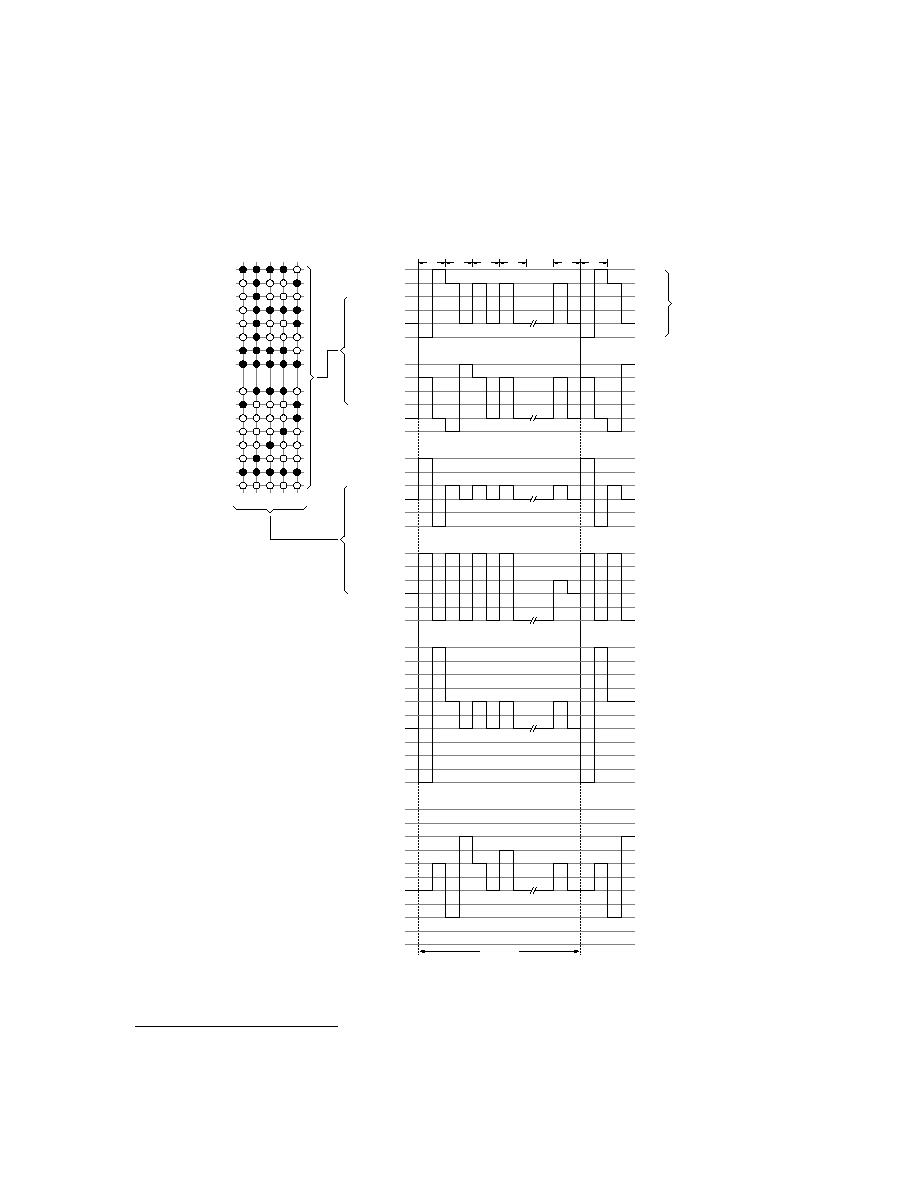
Figure 10, below, illustrates a 1/5 bias, 1/16 duty cycle, Type B configuration, together with COM and SEG wave-
forms. This example uses the dot-matrix configuration for display.
V
DD
V
a
V
b
V
c
V
d
V
e
COM 0
1
V
LCD
V
DD
V
a
V
b
V
c
V
d
V
e
COM 0
2
1
2
3
4
16
1
V
DD
V
a
V
b
V
c
V
d
V
e
SEG 0
1
V
DD
V
a
V
b
V
c
V
d
V
e
SEG 0
2
V
LCD
4
/
5
V
LCD
3
/
5
V
LCD
2
/
5
V
LCD
1
/
5
V
LCD
0
-
1
/
5
V
LCD
-
2
/
5
V
LCD
-
3
/
5
V
LCD
-
4
/
5
V
LCD
-V
LCD
V
LCD
4
/
5
V
LCD
3
/
5
V
LCD
2
/
5
V
LCD
1
/
5
V
LCD
0
-
1
/
5
V
LCD
-
2
/
5
V
LCD
-
3
/
5
V
LCD
-
4
/
5
V
LCD
-V
LCD
1 Frame
COM 0
1
- SEG 0
1
(Select Waveform)
COM 0
2
- SEG 0
2
(Non-Select Waveform)
0
1
0
2
0
3
0
4
0
5
0
6
0
7
0
8
0
9
0
10
0
11
0
12
0
13
0
14
0
15
0
16
0
1
0
2
0
3
0
4
0
5
V
a
= V
DD
-
1
/
5
V
LCD
V
b
= V
DD
-
2
/
5
V
LCD
V
c
= V
DD
-
3
/
5
V
LCD
V
d
= V
DD
-
4
/
5
V
LCD
V
e
= V
DD
-
5
/
5
V
LCD
Figure 10. A 1/5 bias, 1/16 duty cycle, Type B Configuration and Waveforms
≠≠≠≠≠≠≠≠≠≠≠≠≠≠≠≠≠≠≠≠≠≠≠≠≠≠≠≠≠≠≠≠≠≠≠≠≠≠≠≠≠≠≠≠≠≠≠≠≠≠≠≠≠≠≠≠≠≠≠≠≠≠≠≠≠≠≠≠≠≠≠≠≠≠≠≠≠≠≠≠≠≠≠≠≠≠≠≠
s
s
8
OKI SEMICONDUCTOR
Larger configurations are simply extensions of the above principles. OKI Semiconductor supplies a range of single-
chip and multi-chip solutions for multiplexed LCD driver configurations supporting any required number of dots or
segments. The table below lists single-chip LCD drivers, indicating major differences for each part.
For larger dot configurations, such as found in laptop displays for example, common and segment drivers are located
on separate chips.
The table below shows critical features for ICs that provide common drivers only. Note the use of thin quad flat packs
(TQFPs) and Tape Automated Bonding (TAB) for devices with higher lead counts.
The next table, opposite, shows the same critical features for ICs that provide segment drivers only.
[1] On-chip bias resistors.
Single-Chip LCD Drivers for Multiplexed Configurations
Part Number
Dots
Duty Cycle Ratio
On-Chip
Oscillator
Drive Voltage
(V
LCD
)
Package
MSM6544
42
1/2
3.0 - 6.0
56-lead PQFP
MSM6606
40
1/2
X
4.5 - 5.5
64-lead PQFP
MSM6660-01
62
1/2
X
4.0 - 6.0
80-lead PQFP
MSM6660-02
62
1/3
X
[1]
4.0 - 6.0
80-lead PQFP
MSM6660-03
62
1/3
X
[1]
4.0 - 6.0
80-lead PQFP
MSM5265
80
1/2
3.0 - 6.0
100-lead PQFP
MSM5260
80
1/32 - 1/64
X
8.0 - 18.0
100-lead PQFP
MSC5301B-01
16 COM
64 SEG
1/16
X
4.0 - 16.0
100-lead PQFP
MSC5301B-02
8 COM
64 SEG
1/8
X
4.0 - 16.0
100-lead PQFP
Common Drivers for Multiplexed Configurations
Part Number
Drivers
Duty Cycle Ratio
Max. Dots
Drive Voltage
(V
LCD
)
Package
MSM5238
32
1/32 - 1/64
2,048
3.0 - 16.0
44-lead PQFP
MSM5298A
68
1/64 - 1/256
17,408
8.0 - 28.0
80-lead TQFP
MSM6368
80
1/256 - 1/480
38,400
25.0 - 40.0
100-lead TQFP
Segment Drivers for Multiplexed Configurations
Part Number
Drivers
Duty Cycle
Ratio
Max. Dots
Inputs
Drive Voltage
(V
LCD
)
Package
MSM5259
40
1/8 - 1/16
640
1
3.0 - 6.0
56-lead PQFP
MSM5839B
40
1/32 - 1/128
5,120
1
8.0 - 18.0
56-lead PQFP
MSM5839C
40
1/3 - 1/64
2,560
1
4.0 - 11.0
56-lead PQFP
MSM5299A
80
1/64 - 1/256
20,480
4
8.0 - 28.0
100-lead PQFP
s
s
≠≠≠≠≠≠≠≠≠≠≠≠≠≠≠≠≠≠≠≠≠≠≠≠≠≠≠≠≠≠≠≠≠≠≠≠≠≠≠≠≠≠≠≠≠≠≠≠≠≠≠≠≠≠≠≠≠≠≠≠≠≠≠≠≠≠≠≠≠≠≠≠≠≠≠≠≠≠≠≠≠≠≠≠≠≠≠≠≠
9
OKI SEMICONDUCTOR
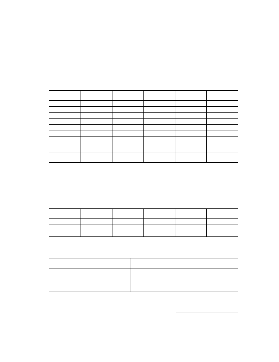
POWER SUPPLY
The table below shows the relationship between the required number of driving biases and the display duty ratios.
Either passive or active bias generation circuitry can provide the required voltage levels, as described in the next two
subsections.
Passive Bias Generation
A resistor ladder is the most common way to generate the required bias voltage levels. Figure 11 below shows a typ-
ical resistor ladder. V
REF
may be tied to V
SS
, or, for displays with larger voltage bias ranges, V
REF
may be tied to a
negative power source.
MSM5299A-01
80
1/64 - 1/256
20,480
4
8.0 - 28.0
100-lead TQFP
MSM5299C
80
1/64 - 1/256
20,480
4
8.0 - 28.0
100-lead PQFP
MSM6669
80
1/100 - 1/256
20,480
4
14.0 - 28.0
0.25mm TAB
Relationship between Duty Cycle and Driving Bias
Duty Ratio
Drive Bias
Voltage Levels
Static
≠
2
1/2
1/2
3
1/3
1/3
4
1/4
1/3
4
1/7
1/4
5
1/8
1/4
5
1/11
1/4
5
1/12
1/4
5
1/14
1/5
6
1/16
1/5
6
1/24
1/5
6
1/32
1/5
6
1/64
1/5
6
Segment Drivers for Multiplexed Configurations (Continued)
Part Number
Drivers
Duty Cycle
Ratio
Max. Dots
Inputs
Drive Voltage
(V
LCD
)
Package
≠≠≠≠≠≠≠≠≠≠≠≠≠≠≠≠≠≠≠≠≠≠≠≠≠≠≠≠≠≠≠≠≠≠≠≠≠≠≠≠≠≠≠≠≠≠≠≠≠≠≠≠≠≠≠≠≠≠≠≠≠≠≠≠≠≠≠≠≠≠≠≠≠≠≠≠≠≠≠≠≠≠≠≠≠≠≠≠
s
s
10
OKI SEMICONDUCTOR
The required operating margin and power consumption determines the appropriate resistor values. Because the LCD
load is capacitive, the current during element charging and discharging distorts the waveform. Generally, the value
of resistor R is 1 k
to 10 k
. Lower resistor values reduce distortion but increase power dissipation. Larger LCD
panels exhibit greater capacitance, and so resistor values may be decreased proportionally as the display size
increases.
No capacitor is required, but a 1-
µ
F capacitor can be used if necessary. Connecting a capacitor in parallel to the resis-
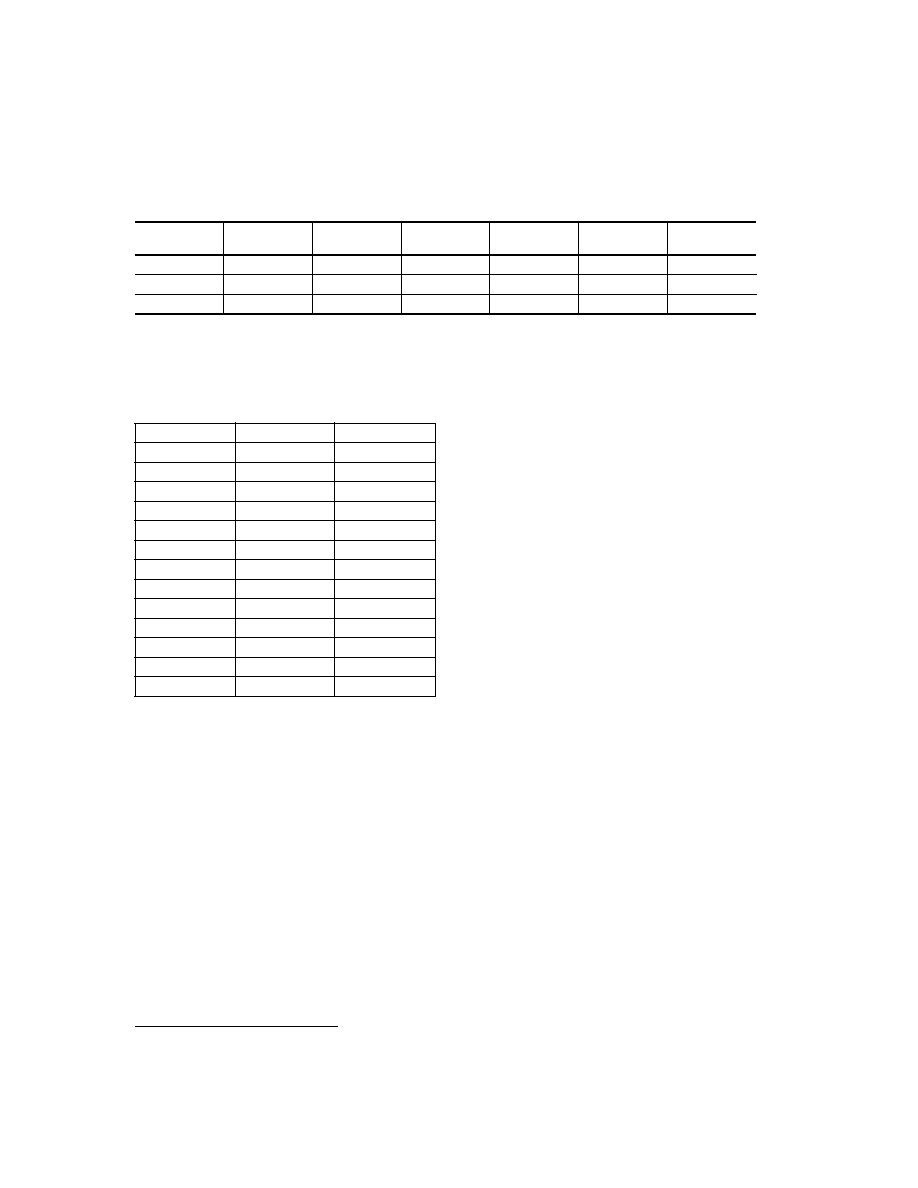
tors can reduce waveform distortion during the charge and discharge periods, but only to a limited degree. Larger
capacitor values generate a voltage level shift and reduce the operating margin. Figure 12 below illustrates how to
connect capacitors in a passive bias network.
In large arrays, the LCD source and common signals form a matrix configuration that complicate the path of the
charge/discharge current through the load. Moreover, current varies according to the demand for the power consump-
tion of the equipment in which the LCD is incorporated. As a result, it is not possible to generate precise equations
for calculating resistor and capacitor values.
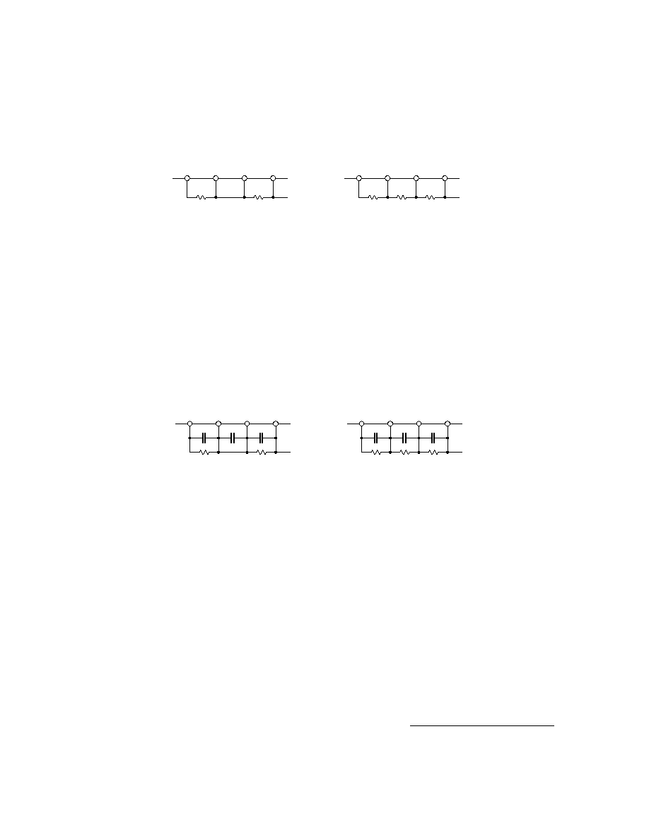
Active Bias Generation
In larger displays, such as graphic displays, the liquid crystal is larger and the duty cycle ratio is smaller. Stability of
the liquid crystal's drive level is therefore more important for a large display than for a small display.
Because graphic displays are large and contain many picture elements, the LCD driver's impedance produces distor-
tion in the drive waveforms and degrades display quality. For this reason, the impedance of the LCD driver bias
sources should be reduced with operational amplifiers. Figure 13 below shows examples of op amp configurations
to provide this reduced impedance.
R
LCD
R
LCD
V
DD
VLC1
VLC2
VLC3
For 1/2 bias (when 1/2 duty is selected)
R
LCD
R
LCD
V
DD
VLC1
VLC2
VLC3
For 1/3 bias (when 1/3 duty is selected)
R
LCD
Figure 11. Network for Simple Passive Bias Generation
V
REF
V
REF
R
LCD
R
LCD
V
DD
VLC1
VLC2
VLC3
For 1/2 bias (when 1/2 duty is selected)
R
LCD
R
LCD
V
DD
VLC1
VLC2
VLC3
For 1/3 bias (when 1/3 duty is selected)
R
LCD
Figure 12. Network for Passive Bias Generation with Capacitor Filters
C
C
C
C
C
C
V
REF
V
REF
s
s
≠≠≠≠≠≠≠≠≠≠≠≠≠≠≠≠≠≠≠≠≠≠≠≠≠≠≠≠≠≠≠≠≠≠≠≠≠≠≠≠≠≠≠≠≠≠≠≠≠≠≠≠≠≠≠≠≠≠≠≠≠≠≠≠≠≠≠≠≠≠≠≠≠≠≠≠≠≠≠≠≠≠≠≠≠≠≠≠≠
11
OKI SEMICONDUCTOR
No load current flows through the dividing resistors because of the high input impedance of the operational amplifi-
ers. A resistor value for R of 10 k
is suitable for the above circuit.
APPLICATION CIRCUITS
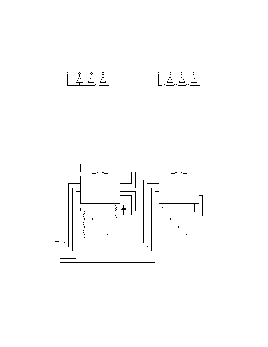
This application note concludes with two illustrative application circuits. The first, shown in Figure 14 below, uses
two MSM6660 LCD drivers to provide three bias signals and 124 segment drivers for a 1/3 bias, 1/3 duty cycle, Type
B LCD panel containing 372 dots.
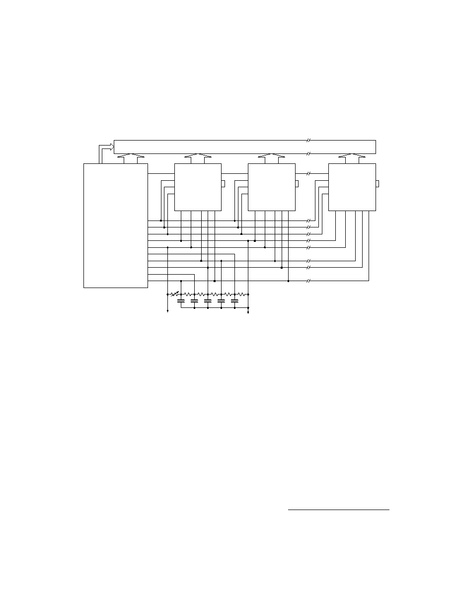
In the example on the previous page, a microcontroller may be necessary to provide an appropriate interface to the
overall system. Figure 15 below depicts a more complex example that may not require an additional microcontroller.
R
LCD
R
LCD
V
DD
VLC1
VLC2
VLC3
For 1/2 bias (when 1/2 duty is selected)
R
LCD
R
LCD
V
DD
VLC1
VLC2
VLC3
For 1/3 bias (when 1/3 duty is selected)
R
LCD
Figure 13. Network for Active Bias Generation
V
REF
V
REF
R
LCD
SEL VLC1 VLC2 VLC3
R
0
C
0
OSC
SYNC
COMOUT
COM3
COM2
COM1
CE
DATA
CK
BL
BL
CK
DATA
CE1
CE2
SEL VLC1 VLC2 VLC3 OSC
SYNC
COMOUT
COM3
COM2
COM1
CE
DATA
CK
BL
R
LCD
R
LCD
SEG0 ~ SEG61
SEG0 ~ SEG61
LCD Panel
Figure 14. Application Circuit Example Using MSM6660 LCD Drivers
≠≠≠≠≠≠≠≠≠≠≠≠≠≠≠≠≠≠≠≠≠≠≠≠≠≠≠≠≠≠≠≠≠≠≠≠≠≠≠≠≠≠≠≠≠≠≠≠≠≠≠≠≠≠≠≠≠≠≠≠≠≠≠≠≠≠≠≠≠≠≠≠≠≠≠≠≠≠≠≠≠≠≠≠≠≠≠≠
s
s
12
OKI SEMICONDUCTOR
Instead of using a separate LCD driver and microcontroller, this circuit integrates LCD driver and controller func-
tions in the MSM6222GS LCD Controller, available from OKI Semiconductor.
LCD controllers can increase system integration and provide a more comprehensive feature set. For small and mid-
size displays, a single LCD controller may provide all the required COM and SEG signals. For larger configurations,
combinations of LCD controllers and drivers can provide exactly the required degree of functionality. In the above
example, the LCD controller provides all required COM signals and some of the SEG signals. Additional SEG driv-
ers augment the LCD controller with the additional SEG drivers required.
OKI Semiconductor provides a family of advanced LCD controllers and drivers that augment the basic functionality
of standard LCD drivers and controllers with enhanced capabilities. Additional features found in OKI's LCD con-
trollers include key-scan logic, power saving modes, on-chip RAM, integrated oscillators, and optional on-chip bias
generation. The table on the following page lists some of the members of OKI's advanced LCD controller/driver fam-
ily.
The following table lists the main features of devices in OKI's advanced LCD controller/driver family described in
this document.
DO
CP
L
DF
V
DD
GND
V
1
V
2
V
3
V
4
V
5
DI
1
CP
LOAD
DF
V
DD
V
SS
V
2
V
3
V
5
DO
40
DO
20
DI
21
0
1
~ 0
40
DI
1
CP
LOAD
DF
V
DD
V
SS
V
2
V
3
V
5
DO
40
DO
20
DI
21
0
1
~ 0
40
DI
1
CP
LOAD
DF
V
DD
V
SS
V
2
V
3
V
5
DO
40
DO
20
DI
21
0
1
~ 0
40
SEG1 ~ 40
COM1 ~ 16
MSM5259GS
MSM5259GS
MSM5259GS
LCD Panel
MSM6222GS
R
0V
C
C
R
C
C
R
R
R
C
+5V
Figure 15. Typical Application Circuit Using the MSM6222GS LCD Controller
s
s
≠≠≠≠≠≠≠≠≠≠≠≠≠≠≠≠≠≠≠≠≠≠≠≠≠≠≠≠≠≠≠≠≠≠≠≠≠≠≠≠≠≠≠≠≠≠≠≠≠≠≠≠≠≠≠≠≠≠≠≠≠≠≠≠≠≠≠≠≠≠≠≠≠≠≠≠≠≠≠≠≠≠≠≠≠≠≠≠≠
13
OKI SEMICONDUCTOR
For more information, see the LCD Driver Controller Data Book and Advanced LCD Controller/Driver Products
from OKI Semiconductor, or contact your local OKI Semiconductor sales representative for additional assistance.
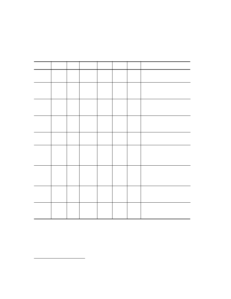
OKI's Advanced LCD Controller/Driver Family
Part No.
Controller
Drivers
Duty Cycle
V
LCD
Interface
Pins /
Package
Special Features
MSM5298A
--
68 COM 1/64 - 1/256
8.0- 28.0
Serial shift
register I/O
80/ PQFP
Bidirectional 68-bit shift register
Multi-chip configuration support
On-chip or external bias generation
MSM5299A
--
80 SEG
1/64 - 1/256
8.0- 28.0
4-bit shift
register I/O
100/
PQFP
Bidirectional 4x20-bit shift register
80-bit latch
Multi-chip configuration support
On-chip or external bias generation
MSC5301B-
01
--
64 SEG
16 COM
1/16
(1/5 bias)
4.0 - 16.0
Serial
MCU
interface
100/
PQFP
1 kbit on-chip RAM
Multi-chip configuration support
Blanking support
On-chip RC oscillator
MSC5301B-
02
--
64 SEG
8 COM
1/8
(1/4 bias)
4.0 - 16.0
Serial
MCU
interface
100/
PQFP
1 kbit on-chip RAM
Multi-chip configuration support
Blanking support
On-chip RC oscillator
MSM6568A
--
160 COM 1/200 - 1/480 14.0 - 28.0 2-bit shift
register I/O
Slim TAB
Bidirectional 160-bit shift register
Multi-chip configuration support
On-chip or external bias generation
MSM6569
--
160 SEG 1/200 - 1/480 20.0 - 40.0 8-bit shift
register I/O
Slim TAB
Unidirectional 160-bit shift register
160-bit latch
Power-saving mode
Multi-chip configuration support
On-chip or external bias generation
MSM6606
--
40 SEG
2 COM
1/2
5.5
Serial
MCU
interface
64/ PQFP
Internal 5x6 key-scan circuit
(supporting up to 30 key switches)
Single LED driver output
Integrated bias voltage generation
On-chip RC oscillator
MSM6665-
01
80 SEG
17 COM
1/9 or 1/17
3.0 - 6.0
Serial
MCU
interface
128/
PQFP
256 5x7 characters in on-chip ROM
80 dot arbitrators
Character and arbitrator blink functions
On-chip RC oscillator
MSM6665B
80 SEG
17 COM
1/9 or 1/17
--
Serial
MCU
interface
PBGA
256 5x7 characters in on-chip ROM
80 dot arbitrators
Character and arbitrator blink functions
Integrated bias voltage generation