 | –≠–ª–µ–∫—Ç—Ä–æ–Ω–Ω—ã–π –∫–æ–º–ø–æ–Ω–µ–Ω—Ç: MSM6575L | –°–∫–∞—á–∞—Ç—å:  PDF PDF  ZIP ZIP |

1/13
MSM6545/6575/6545L/6575L
° Semiconductor
GENERAL DESCRIPTION
MSM6545/6575/6545L/6575L is a 4-bit, low-power microcontroller manufactured in a CMOS
silicon gate process. The microcontroller can be initialized and operated at a low supply voltage
of 0.9 V.
This single device contains a crystal oscillator circuit, voltage converter circuits, a time base
counter, a ROM, a RAM, a stack RAM, I/O ports, interrupt function components, a serial I/O
port, a buzzer output circuit, and an updown counter.
This IC is driven by one battery and is well suited to products that need to be operated under
low power consumption.
FEATURES
∑ The IC can be initialized and operated even at a low voltage of 0.9 V.
∑ Low power consumption
∑ ROM
: 4096 words • 17 bits (MSM6545/6545L)
2048 words • 17 bits (MSM6575/6575L)
∑ RAM
: 256 words • 4 bits (MSM6545/6545L)
128 words • 4 bits (MSM6575/6575L)
∑ I/O port
Input-output port
: 7 ports • 4 bits
Input port
: 1 port • 4 bits
∑ Interrupt functions (real-time interrupt, external interrupt, and serial interrupt)
∑ Serial I/O port
: 8-bit sync communication
∑ Buzzer output circuit
∑ 4-bit decimal updown counter
∑ 73 instructions
∑ Minimum instruction execution time : 61 ms
∑ Operation under single 1.5 V power supply (MSM6545/6575)
A mask option allows the 3 V power supply to be used (MSM6545L/6575L)
∑ Built-in 32.768 kHz crystal oscillator circuit
∑ Package options:
44-pin plastic QFP (QFP44-P-910-0.80-K)
: (Product name : MSM6545/6545L-••GS-K)
44-pin plastic QFP (QFP44-P-910-0.80-2K) : (Product name : MSM6545/6545L-••GS-2K)
44-pin plastic QFP (QFP44-P-910-0.80-K)
: (Product name : MSM6575/6575L-••GS-K)
44-pin plastic QFP (QFP44-P-910-0.80-2K) : (Product name : MSM6575/6575L-••GS-2K)
Chip
•• indicates a code number.
° Semiconductor
MSM6545/6575/6545L/6575L
Operatable at 0.9 V and Built-in Buzzer Circuit 4-Bit Microcontroller
E2E0019-38-94
This version: Sep. 1998
Previous version: Mar. 1996
2/13
MSM6545/6575/6545L/6575L
° Semiconductor
BLOCK DIAGRAM
P7.3
P7.2
P7.1
P7.0
P6.3
P6.2
P6.1
P6.0
P5.3
P5.2
P5.1
P5.0
P4.3
P4.2
P4.1
P4.0
P3.3
P3.2
P3.1
P3.0
P2.3
P2.2
P2.1
P2.0
P1.3
P1.2
P1.1
P1.0
P0.3
P0.2
P0.1
P0.0
XT
XTB
PORT7
PORT6
PORT5
PORT4
PORT3
PORT2
PORT1
PORT0
OSC
TMOUT
TIME BASE
COUNTER
SYSTEM CLOCK
GENERATOR
CCLK
BU/D
4-Bit BCD COUNTER
CCNT
PGCONH
PGCONL
SIN
SOUT
SCKL
MODE
PCZIOX
PCHZX0
PCIOX0
PCHZ0
PCIO0
SCND0
SCND1
SERIAL I/O
SBFFL
SBFFH
D-BUS
EIF
EIRT
I
RQRT
FIEX
I
RQEX
PNEX
I
RQSIO
PRIO
INTERRUPT CONTROL
RAM
MSM6545/6545L...256
•
4 bits
MSM6575/6575L...128
•
4 bits
PAGE
WORK
ADRS
PROGRAM ROM
MSM6545/6545L
... 4096
•
17 bits
MSM6575/6575L
... 2048
•
17 bits
INSTRUCTION
REGISTER
INSTRUCTION
DECODER
STACK RAM
PROGRAM
COUNTER
ADDER
FRMT
FLAG
S-bus
ACC
A
-bus
ALU
MPX
TEMPO
BUZZER
MDTH
MDTL
VOLTAGE
REGULATOR
BD
V
DD
V
SS1
V
SS2
V
EE
V
CP
V
CM
3/13
MSM6545/6575/6545L/6575L
° Semiconductor
PIN CONFIGURATION (TOP VIEW)
33
32
31
30
29
28
27
26
25
24
23
1
2
3
4
5
6
7
8
9
10
11
P4.0
P4.1
P4.2
P4.3
RESET
TEST1
TEST2
TEST3
P7.3/CCLK
P7.2/BU/D
P7.1/SIN
P1.1
P1.0
P0.3
P0.2
P0.1
P0.0
P5.0
P5.1
P5.2
P5.3
BD
44
43
42
41
40
39
38
37
36
35
34
P3.3
P3.2
P3.1
P3.0
P2.3
V
DD
P2.2
P2.1
P2.0
P1.3
P1.2
12
13
14
15
16
17
18
19
20
21
22
P7.0/SOUT
P6.3/
SCLK
P6.0
XTB
XT
V
DD
V
SS1
V
CM
V
CP
V
SS2
V
EE
44-Pin Plastic QFP
Notes: 1. P6.3, P7.0 and P7.1 also function as serial port pins.
P7.2, and P7.3 also function as updown counter pins.
2. P6.1 and P6.2 are not assigned pins.
4/13
MSM6545/6575/6545L/6575L
° Semiconductor
PIN DESCRIPTIONS
Symbol
Type
Description
PORT0
(P0.0 to P0.3)
I/O
4-bit Input-output port, I/O switchable, with/without input pull-down resistor
I/O
4-bit Input-output port, I/O switchable, with/without input pull-down resistor
I/O
4-bit Input-output port, I/O switchable,
with/without input pull-down resistor
I/O
4-bit Input-output port, I/O switchable, with/without input pull-down resistor
I/O
4-bit Input-output port, I/O switchable, with/without input pull-down resistor
I/O
4-bit Input-output port, I/O switchable, with/without input pull-down resistor
I/O
4-bit Input-output port, I/O switchable,
with/without input pull-down resistor
4-bit input port
Tie to the negative pole of the battery when
not used.
BD
O
Buzzer output pin
RESET
I
Reset pin with input pull-down resistor
TEST1
Testing pins with input pull-down resistor
Tie to the negative pole of the battery.
TEST2
I
TEST3
XT
I
Connection pins for crystal oscillator
XTB
O
V
DD
--
0 V power supply pin
V
SS1
--
≠1.5 V supply pin (power supply pin for ≠1.5 V operation)
V
SS2
--
≠3.0 V supply pin (power supply pin for ≠3.0 V operation)
V
CP
--
Connection pins for internal potential development capacitor
V
CM
PORT1
(P1.1 to P1.3)
PORT2
(P2.0 to P2.3)
PORT3
(P3.0 to P3.3)
PORT4
(P4.0 to P4.3)
PORT5
(P5.0 to P5.3)
PORT6
(P6.0 to P6.3)
P2.0 to P2.3
External interrupt
port
P6.3: SCLK
Shared with serial
port
I
PORT7
(P7.0 to P7.3)
P7.0: SOUT
P7.1: SIN
P7.2: BU/D
Shared with 4-bit
up/down counter
P7.3: CCLK
V
EE
--
Supply pin for internal logic (constant voltage circuit output pin)

5/13
MSM6545/6575/6545L/6575L
° Semiconductor
ABSOLUTE MAXIMUM RATINGS (MSM6545/6575, 1.5 V, BUF = "0")
Parameter
Symbol
Condition
Rating
Unit
Power Supply Voltage
V
SS1
Ta = 25∞C
≠6.0 to +0.3
Input Voltage
V
IN
V
SS1
≠ 0.3 to +0.3
V
Output Voltage
V
OUT
V
SS1
≠ 0.3 to +0.3
Storage Temperature
T
STG
--
≠55 to +125
∞C
V
DD
= 0 V (V
SS1
= battery voltage)
Note: The input of the constant voltage circuit is equal to the output of the voltage converter
(V
SS2
).
RECOMMENDED OPERATING CONDITIONS (MSM6545/6575, 1.5 V, BUF = "0")
Parameter
Symbol
Condition
Range
Unit
Operating Voltage
V
op
--
≠1.75 to ≠0.9
V
V
--
Operating Temperature
T
op
≠20 to +70
∞C
--
Oscillation Frequency
f
OSC
32.768
kHz
--
V
DD
= 0 V (V
SS1
= battery voltage)
Note: The input of the constant voltage circuit is equal to the output of the voltage converter
(V
SS2
).
ELECTRICAL CHARACTERISTICS (MSM6545/6575, 1.5 V, BUF = "0")
Parameter
Symbol
Condition
Min.
Applied Pin
Typ. Max. Unit
Power Supply Current
I
DD
*1
--
--
3
--
mA
Oscillation Start Voltage
≠V
OSC
Within 2 seconds
--
V
SS1
--
0.9
V
Output Current 1
≠I
OH1
V
O
= ≠0.5 V
150
PORT0 to PORT6*2
SOUT, SCLK
--
--
mA
I
OL1
V
O
= ≠1.0 V
150
--
--
Output Current 2
≠I
OH2
V
O
= ≠0.5 V
20
BD
--
--
mA
I
OL2
V
O
= ≠1.0 V
20
--
--
Input Current 1
I
IH1
V
I
= 0 V, in the input state,
with pull-down resistor
7
PORT0 to
PORT6 *2
15
30
mA
Input Leakage Current
¡I
IL
¡
V
I
= 0 V, ≠1.5 V, in the input state,
without pull-down resistor
--
PORT0 to PORT7*2
SIN, SOUT, SCLK
--
1
mA
Input Current 3
I
IH3
V
I
= 0 V, with pull-down
resistor
70
RESET
TEST1 to TEST3
250
500
mA
Input Voltage
≠V
IH
--
--
All input pins
--
0.3
V
≠V
IL
1.2
--
--
V
DD
= 0 V, V
SS1
= ≠1.5 V (battery voltage), V
SS2
= ≠3.0 V, f
OSC
= 32.768 kHz, C
X
= 35 pF, Ta = 25∞C
*1 Depends on the program. (Values in the above table are applied in the case where the
software duty is about 5%.)
*2 PORT0 = P0.0 to P0.3, PORT1 = P1.0 to P1.3, PORT2 = P2.0 to P2.3, PORT3 = P3.0 to P3.3,
PORT4 = P4.0 to P4.3, PORT5 = P5.0 to P5.3, PORT6 = P6.0 to P6.3, PORT7 = P7.0 to P7.3
Note: The input of the constant voltage circuit is equal to the output of the voltage converter
(V
SS2
).

6/13
MSM6545/6575/6545L/6575L
° Semiconductor
ABSOLUTE MAXIMUM RATINGS (MSM6545/6575, 1.5 V, BUF = "1")
ELECTRICAL CHARACTERISTICS (MSM6545/6575, 1.5 V, BUF = "1")
Parameter
Symbol
Condition
Min.
Applied Pin
Typ. Max. Unit
Power Supply Current
I
DD
*1
--
--
1.5
--
mA
Oscillation Start Voltage
≠V
OSC
Within 2 seconds
--
V
SS1
--
0.9
V
Output Current 1
≠I
OH1
V
O
= ≠0.5 V
150
PORT0 to PORT6*2
SOUT, SCLK
--
--
mA
I
OL1
V
O
= ≠1.0 V
150
--
--
Output Current 2
≠I
OH2
V
O
= ≠0.5 V
20
BD
--
--
mA
I
OL2
V
O
= ≠1.0 V
20
--
--
Input Current 1
I
IH1
V
I
= 0 V, in the input state,
with pull-down resistor
7
PORT0 to
PORT6 *2
15
30
mA
Input Leakage Current
¡I
IL
¡
V
I
= 0 V, ≠1.5 V, in the input state,
without pull-down resistor
--
PORT0 to PORT7*2
SIN, SOUT, SCLK
--
1
mA
Input Current 3
I
IH3
V
I
= 0 V, without pull-down
resistor
70
RESET
TEST1 to TEST3
250
500
mA
Input Voltage
≠V
IH
--
--
All input pins
--
0.3
V
≠V
IL
1.2
--
--
V
DD
= 0 V, V
SS1
= ≠1.5 V (battery voltage), V
SS2
= ≠3.0 V, f
OSC
= 32.768 kHz, C
X
= 35 pF, Ta = 25∞C
*1 Depends on the program. (Values in the above table are applied in the case where the
software duty is about 5%.)
*2 PORT0 = P0.0 to P0.3, PORT1 = P1.0 to P1.3, PORT2 = P2.0 to P2.3, PORT3 = P3.0 to P3.3,
PORT4 = P4.0 to P4.3, PORT5 = P5.0 to P5.3, PORT6 = P6.0 to P6.3, PORT7 = P7.0 to P7.3
RECOMMENDED OPERATING CONDITIONS (MSM6545/6575, 1.5 V, BUF = "1")
Parameter
Symbol
Condition
Range
Unit
Operating Voltage
V
op
--
≠1.75 to ≠0.9
V
V
--
Operating Temperature
T
op
≠20 to +70
∞C
--
Oscillation Frequency
f
OSC
32.768
kHz
--
V
DD
= 0 V (V
SS1
= battery voltage)
Note: The input of the constant voltage circuit is directly connected to the power supply (V
SS1
).
Parameter
Symbol
Condition
Rating
Unit
Power Supply Voltage
V
SS1
Ta = 25∞C
≠6.0 to +0.3
Input Voltage
V
IN
V
SS1
≠ 0.3 to +0.3
V
Output Voltage
V
OUT
V
SS1
≠ 0.3 to +0.3
Storage Temperature
T
STG
--
≠55 to +125
∞C
V
DD
= 0 V (V
SS1
= battery voltage)
Note: The input of the constant voltage circuit is directly connected to the power supply (V
SS1
).
Note: The input of the constant voltage circuit is directly connected to the power supply (V
SS1
).
7/13
MSM6545/6575/6545L/6575L
° Semiconductor
ABSOLUTE MAXIMUM RATINGS (MSM6545L/6575L, 3.0 V, BUF = "0")
Parameter
Symbol
Condition
Rating
Unit
Power Supply Voltage
V
SS2
Ta = 25∞C
≠6.0 to +0.3
Input Voltage
V
IN
V
SS2
≠ 0.3 to +0.3
V
Output Voltage
V
OUT
V
SS2
≠ 0.3 to +0.3
Storage Temperature
T
STG
--
≠55 to +125
∞C
V
DD
= 0 V (V
SS2
= battery voltage)
RECOMMENDED OPERATING CONDITIONS (MSM6545L/6575L, 3.0 V, BUF = "0")
Parameter
Symbol
Condition
Range
Unit
Operating Voltage
V
op
--
≠3.5 to ≠1.8
V
V
--
Operating Temperature
T
op
≠20 to +70
∞C
--
Oscillation Frequency
f
OSC
32.768
kHz
--
V
DD
= 0 V (V
SS2
= battery voltage)
ELECTRICAL CHARACTERISTICS (MSM6545L/6575L, 3.0 V, BUF = "0")
Parameter
Symbol
Condition
Min.
Applied Pin
Typ. Max. Unit
Power Supply Current
I
DD
*1
--
--
0.75
--
mA
Oscillation Start Voltage
≠V
OSC
Within 2 seconds
--
V
SS2
--
1.8
V
Output Current 1
≠I
OH1
V
O
= ≠0.5 V
500
PORT0 to PORT6*2
SOUT, SCLK
--
--
mA
I
OL1
V
O
= ≠2.5 V
500
--
--
Output Current 2
≠I
OH2
V
O
= ≠0.5 V
20
BD
--
--
mA
I
OL2
V
O
= ≠2.5 V
20
--
--
Input Current 1
I
IH1
V
I
= 0 V, in the input state,
with pull-down resistor
50
PORT0 to
PORT6 *2
100
200
mA
Input Leakage Current
¡I
IL
¡
V
I
= 0 V, ≠3 V, in the input state,
without pull-down resistor
--
PORT0 to PORT7*2
SIN, SOUT, SCLK
--
1
mA
Input Current 3
I
IH3
V
I
= 0 V, with pull-down
resistor
200
RESET
TEST1 to TEST3
750 1500
mA
Input Voltage
≠V
IH
--
--
All input pins
--
0.5
V
≠V
IL
2.5
--
--
V
DD
= 0 V, V
SS1
= ≠1.5 V, V
SS2
= ≠3.0 V (battery voltage), f
OSC
= 32.768 kHz, C
X
= 35 pF, Ta = 25∞C
Note: The input of the constant voltage circuit is equal to the output of the voltage converter
(V
SS1
).
*1 Depends on the program. (Values in the above table are applied in the case where the
software duty is about 5%.)
*2 PORT0 = P0.0 to P0.3, PORT1 = P1.0 to P1.3, PORT2 = P2.0 to P2.3, PORT3 = P3.0 to P3.3,
PORT4 = P4.0 to P4.3, PORT5 = P5.0 to P5.3, PORT6 = P6.0 to P6.3, PORT7 = P7.0 to P7.3
Note: The input of the constant voltage circuit is equal to the output of the voltage converter
(V
SS1
).
Note: The input of the constant voltage circuit is equal to the output of the voltage converter
(V
SS1
).
8/13
MSM6545/6575/6545L/6575L
° Semiconductor
ABSOLUTE MAXIMUM RATINGS (MSM6545L/6575L, 3.0 V, BUF = "1")
Parameter
Symbol
Condition
Rating
Unit
Power Supply Voltage
V
SS2
Ta = 25∞C
≠6.0 to +0.3
Input Voltage
V
IN
V
SS2
≠ 0.3 to +0.3
V
Output Voltage
V
OUT
V
SS2
≠ 0.3 to +0.3
Storage Temperature
T
STG
--
≠55 to +125
∞C
V
DD
= 0 V (V
SS2
= battery voltage)
Note: The input of the constant voltage circuit is directly connected to the power supply (V
SS2
).
RECOMMENDED OPERATING CONDITIONS (MSM6545L/6575L, 3.0 V, BUF = "1")
Parameter
Symbol
Condition
Range
Unit
Operating Voltage
V
op
--
≠3.5 to ≠0.9
V
V
--
Operating Temperature
T
op
≠20 to +70
∞C
--
Oscillation Frequency
f
OSC
32.768
kHz
--
V
DD
= 0 V (V
SS2
= battery voltage)
Note: The input of the constant voltage circuit is directly connected to the power supply (V
SS2
).
ELECTRICAL CHARACTERISTICS (MSM6545L/6575L, 3.0 V, BUF = "1")
Parameter
Symbol
Condition
Min.
Applied Pin
Typ. Max. Unit
Power Supply Current
I
DD
*1
--
--
1.5
--
mA
Oscillation Start Voltage
≠V
OSC
Within 2 seconds
--
V
SS2
--
0.9
V
Output Current 1
≠I
OH1
V
O
= ≠0.5 V
500
PORT0 to PORT6*2
SOUT, SCLK
--
--
mA
I
OL1
V
O
= ≠2.5 V
500
--
--
Output Current 2
≠I
OH2
V
O
= ≠0.5 V
20
BD
--
--
mA
I
OL2
V
O
= ≠2.5 V
20
--
--
Input Current 1
V
I
= 0 V, in the input state,
with pull-down resistor
50
PORT0 to
PORT6 *2
100
200
mA
Input Leakage Current
¡I
IL
¡
V
I
= 0 V, ≠3 V, in the input state,
without pull-down resistor
--
PORT0 to PORT7*2
SIN, SOUT, SCLK
--
1
mA
Input Current 3
I
IH3
V
I
= 0 V, with pull-down
resistor
200
RESET
TEST1 to TEST3
750 1500
mA
Input Voltage
≠V
IH
--
--
All input pins
--
0.5
V
≠V
IL
2.5
--
--
V
DD
= 0 V, V
SS1
= ≠1.5 V, V
SS2
= ≠3.0 V (battery voltage), f
OSC
= 32.768 kHz, C
X
= 35 pF, Ta = 25∞C
I
IH1
*1 Depends on the program. (Values in the above table are applied in the case where the
software duty is about 5%.)
*2 PORT0 = P0.0 to P0.3, PORT1 = P1.0 to P1.3, PORT2 = P2.0 to P2.3, PORT3 = P3.0 to P3.3,
PORT4 = P4.0 to P4.3, PORT5 = P5.0 to P5.3, PORT6 = P6.0 to P6.3, PORT7 = P7.0 to P7.3
Note: The input of the constant voltage circuit is directly connected to the power supply (V
SS2
).
9/13
MSM6545/6575/6545L/6575L
° Semiconductor
NOTES ON USE
Power Supply for 0.9 V Microcontroller Series (Backup Flag and Constant-Voltage Circuit)
The 0.9 V devices have a built-in constant-voltage circuit. The output of this constant-voltage
circuit powers the microcontroller's internal logic circuits. Setting a backup flag (BUF) allows
the input of the constant voltage circuit to be switched to either the battery or the output
generated in the voltage converter, based on the battery voltage. A battery voltage of 1.5 V or
3.0 V can be selected.
The output (V
EE
) of the constant-voltage circuit is set at approximately ≠1.3 V. This allows the
current consumed by the internal logic to be limited, irrespective of the battery voltage.
However, if the input of the constant voltage circuit is below this set value (approximately ≠
1.3V), the output (V
EE
) is equal to the input. The 0.9 V microcontroller can be operated even if
the internal voltage (output from the constant voltage circuit) falls to 0.9 V. Setting the backup
flag allows a larger operating voltage margin despite changes in internal voltage due to noise.
For example, for the 1.5 V specification, setting the backup flag at "0" supplies twice the battery
voltage to the constant voltage circuit. Thus, even if the battery voltage falls to 0.9 V, the output
voltage (V
EE
) is maintained at ≠1.3 V, providing a larger margin of operating voltage of the
internal logic circuits, because 1.8 V is applied to the input of the constant-voltage circuit.
Figures 1 to 4 show the internal status depending on the backup flag settings for the battery, as
well as status features.
XTAL
V
DD
(0 V)
V
SS1
(≠1.5 V)
V
SS2
(≠3.0 V)
V
SS3
*
(≠4.5 V)
V
EE
(About≠1.3 V)
LCD driver*
Voltage converter
Backup flag
(BUF)
Constant voltage circuit
VR
Internal logic
XT
XTB
* The V
SS3
pin is provided for the devices that contain an
LCD driver.
10/13
MSM6545/6575/6545L/6575L
° Semiconductor
(Figure 1) 1.5 V Operation (Backup Flag = 1)
Voltage converter
VR
Internal
logic
V
DD
= 0 V
V
B
= ≠1.5 V
(≠3.0 V)
V
EE
V
DD
V
SS1
V
SS2
Voltage
doubler
Internal
status
Operating
range
Current
consumption
Feature
The battery level V
SS1
is applied
to the input of the constant voltage circuit.
≠0.9 to ≠1.75 V
1.5 mA*
When the battery level is powered down, the
internal circuit is powered directly by the
battery.
* When the software duty is about 5%
(Figure 2) 1.5 V Operation (Backup Flag = 0)
Feature
Internal
status
Internal
logic
Voltage
doubler
Voltage converter
VR
V
DD
= 0 V
V
B
= ≠1.5 V
(≠3.0 V)
V
EE
V
DD
V
SS1
V
SS2
Operating
range
Current
consumption
A doubled level of V
SS2
is applied to the input
of the constant voltage circuit.
≠0.9 to ≠1.75 V
3 mA*
When the battery level is powered down, a
larger operating voltage margin is gained,
compared to the case of Figure 1.
* When the software duty is about 5%
(Figure 3) 3.0 V Operation (Backup Flag = 1)
Voltage
doubler
Voltage converter
VR
V
DD
= 0 V
V
B
= ≠3.0 V
(≠1.5 V)
V
EE
V
DD
V
SS1
V
SS2
Feature
Internal
status
Operating
range
Current
consumption
The battery level V
SS2
is applied to the input
of the constant voltage circuit.
≠0.9 to ≠3.5 V
1.5 mA*
When the battery level is powered down, the
internal circuit is powered directly by the
battery.
Internal
logic
* When the software duty is about 5%
11/13
MSM6545/6575/6545L/6575L
° Semiconductor
(Figure 4) 3.0 V Operation (Backup Flag = 0)
Voltage
doubler
Voltage converter
VR
V
DD
= 0 V
V
B
= ≠3.0 V
(≠1.5 V)
V
EE
V
DD
V
SS1
V
SS2
Feature
Internal
status
Operating
range
Current
consumption
A doubled level of V
SS1
is applied to the
input of the constant voltage circuit.
≠1.8 to ≠3.5 V
When the battery level is powered down, a
smaller operating voltage margin is gained,
compared to the case of Figure 3.
Internal
logic
0.75 mA*
* When the software duty is about 5%
12/13
MSM6545/6575/6545L/6575L
° Semiconductor
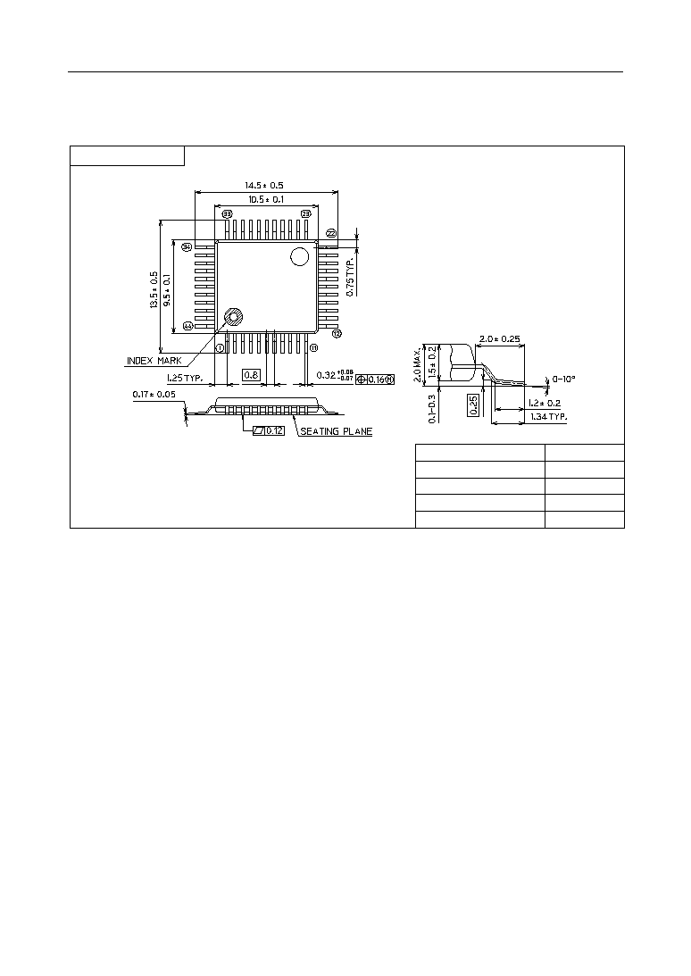
(Unit : mm)
PACKAGE DIMENSIONS
Notes for Mounting the Surface Mount Type Package
The SOP, QFP, TSOP, SOJ, QFJ (PLCC), SHP and BGA are surface mount type packages, which
are very susceptible to heat in reflow mounting and humidity absorbed in storage.
Therefore, before you perform reflow mounting, contact Oki's responsible sales person for the
product name, package name, pin number, package code and desired mounting conditions
(reflow method, temperature and times).
QFP44-P-910-0.80-K
Package material
Lead frame material
Pin treatment
Solder plate thickness
Package weight (g)
Epoxy resin
42 alloy
Solder plating
5 mm or more
0.35 TYP.
Mirror finish
13/13
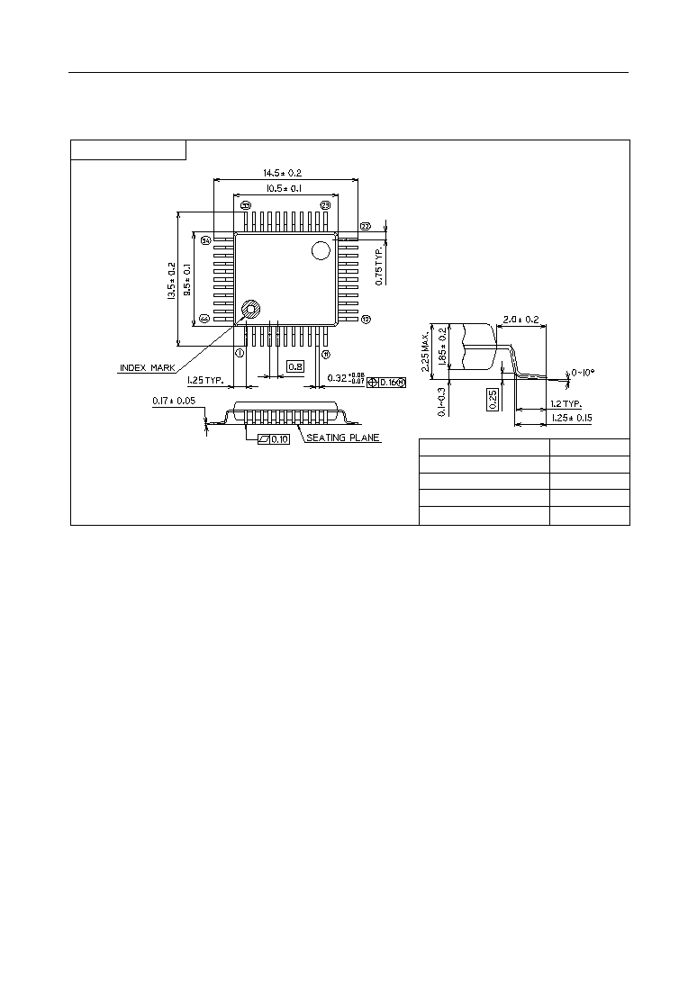
MSM6545/6575/6545L/6575L
° Semiconductor
(Unit : mm)
Notes for Mounting the Surface Mount Type Package
The SOP, QFP, TSOP, SOJ, QFJ (PLCC), SHP and BGA are surface mount type packages, which
are very susceptible to heat in reflow mounting and humidity absorbed in storage.
Therefore, before you perform reflow mounting, contact Oki's responsible sales person for the
product name, package name, pin number, package code and desired mounting conditions
(reflow method, temperature and times).
Package material
Lead frame material
Pin treatment
Solder plate thickness
Package weight (g)
Epoxy resin
42 alloy
Solder plating
5 mm or more
0.41 TYP.
QFP44-P-910-0.80-2K
Mirror finish