 | –≠–ª–µ–∫—Ç—Ä–æ–Ω–Ω—ã–π –∫–æ–º–ø–æ–Ω–µ–Ω—Ç: MSM6585RS | –°–∫–∞—á–∞—Ç—å:  PDF PDF  ZIP ZIP |
OKI Semiconductor
FEDL6585-03
Issue Date: Aug. 25, 2004
MSM6585
ADPCM Voice Synthesis IC
1
GENERAL DESCRIPTION
The MSM6585 is an version-up product of the MSM5205 voice synthesis IC. Mainly improved points
are improvement for the precision of an internal DA converter, a built-in low-pass filter, and
expansion on the sampling frequency. The MSM6585 does not include a control circuit to drive an
external memory similar to the MSM5205. Therefore, the MSM6585 can be connected with not only
semiconductor memories, but other memory media (CD-ROM, etc.) by the control of CPU.
FEATURES
∑ 4-bit ADPCM method
∑ Built-in 12-bit DA converter
∑ Built-in low-pass filter (LPF) (≠40dB/oct)
∑ Sampling frequencies: 4k/8k/16k/32kHz
∑ Master clock frequency (ceramic oscillator) : 640kHz
∑
Voice data synthesis: Supported by voice analysis editing tool AR207
∑
Package options:
18-pin plastic DIP (DIP18-P-300-2.54) (MSM6585RS)
24-pin plastic SOP (SOP24-P-430-1.27-K) (MSM6585MAZXXX)
30-pin plastic SSOP (SSOP30-P-56-0.65-K) (MSM6585MBZXXX)
DIFFERENCES BETWEEN MSM6585 AND MSM5205
MSM6585
MSM5205
∑ Master clock frequency:
640kHz
384kHz
∑ Sampling frequency:
4k/8k/16k/32kHz
4k/6k/8kHz
∑ ADPCM bit length:
4-bit
3-bit/4-bit
∑ DA Converter:
12-bit
10-bit
∑ Low-pass filter:
Included (≠40dB/oct)
Not included
∑ Overflow preventing circuit:
Included
Not included
∑ Power supply voltage:
4.5 to 5.5V
3.0 to 6.0V
∑ Operating current consumption:
10mA
4mA
∑ Operating temperature:
≠40 to +85
∞
C
≠30 to +70
∞
C
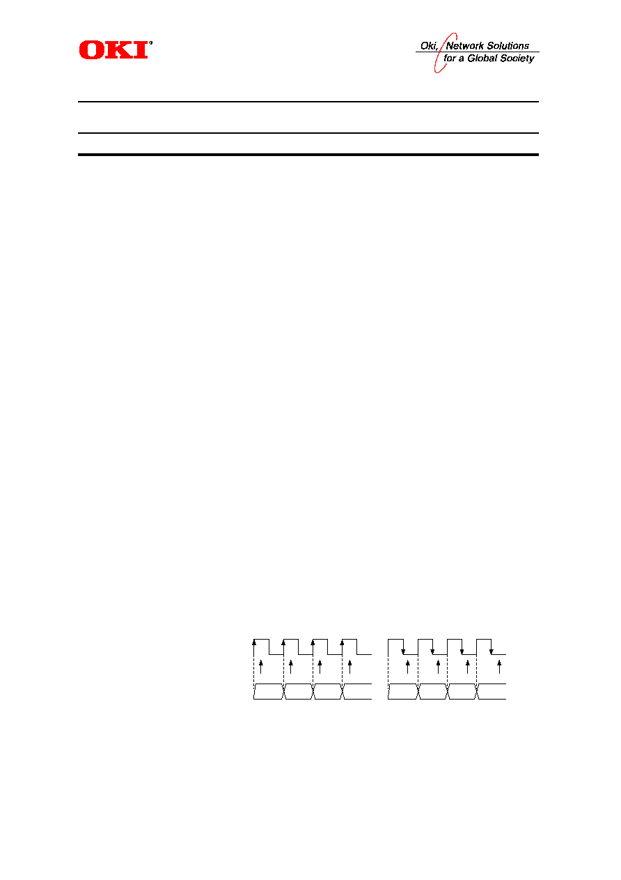
∑ D3 to D0 input timing
VCK (O)
D3 - D0
input timing
ADPCM Data
MSM6585
MSM5205

° Semiconductor
2
MSM6585
BLOCK DIAGRAM
≠
+
D3
D2
D1
D0
AOUT
DAO
V
DD
GND
4
12
4-Bit
LATCH
ADPCM
Synthesizer
12-Bit DAC
LPF
OSC
Timing Controller
TEST CIRCUIT
XT
XT
S1 S2
RESET
VCK
T1
T2 T3 T4
° Semiconductor
3
MSM6585
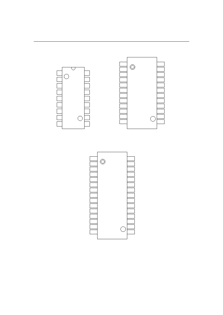
PIN CONFIGURATION (TOP VIEW)
18-Pin Plastic DIP
S1
S2
T3
D0
D1
D2
D3
T4
GND
V
DD
XT
XT
RESET
VCK
T2
T1
DAO
AOUT
1
2
3
4
5
6
7
8
9
18
17
16
15
14
13
12
11
10
1
2
3
4
5
6
7
8
9
10
11
12
S1
S2
T3
NC
D0
NC
D1
D2
NC
D3
T4
GND
V
DD
XT
XT
NC
RESET
NC
VCK
T2
T1
NC
DAO
AOUT
24
23
22
21
20
19
18
17
16
15
14
13
NC : No connection
24-Pin Plastic SOP
1
2
3
4
5
6
7
8
9
10
11
12
S1
S2
NC
NC
NC
T3
D0
D1
D2
D3
NC
NC
V
DD
XT
NC
NC
NC
XT
RESET
VCK
T2
T1
NC
NC
30
29
28
27
26
25
24
23
22
21
20
19
NC : No connection
30-Pin Plastic SSOP
13
14
15
NC
T4
GND
NC
DAO
AOUT
18
17
16

° Semiconductor
4
MSM6585
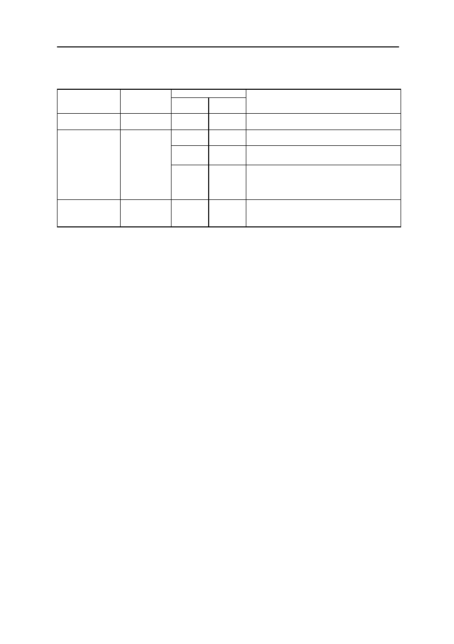
PIN DESCRIPTION
Symbol Type
Description
S1
I
Pins to determine the sampling frequency.
The sampling frequencies of 32k, 16k, 8k, and 4kHz can be selected by
combinations. (See the sampling frequencies in FUNCTIONAL
DESCRIPTION on the selection of combinations.)
T3
I
Pin to test the internal circuit. Set this pin to a high level or make it open
because it has a built-in pull-up resistor.
D0-D3
I
Input pins for ADPCM data.
T4
O
Pin to test the internal circuit. Make this pin open.
GND
--
Ground pin
AOUT
O
Pin to output the analog voice from the low-pass filter. Connect a 0.01 mF
capacitor to this pin. (See the AOUT connecting circuit in FUNCTIONAL
DESCRIPTION on the connecting circuit.)
DAO
O
Pin to output the analog voice from the DA converter.
T1
I
Pins to test the internal circuit. Set these pins to a low level or make them
open because pull-down resistors are included.
VCK
O
This pin outputs the sampling frequency selected by the combinations of
S1 and S2.
The voice synthesis starts or stops by synchronizing with VCK.
RESET
I
Reset pin. The voice synthesis circuit is initialized by synchronizing with
VCK. If this pin is set to a high level, the D0 to D3 data inputs are disabled
by synchronizing with VCK. The AOUT and DA0 pins output 1/2 V
DD
and
become the state of no voice.
XT
I
Pin to connect an oscillator. When the external clock is used, input it
from this pin.
XT
O
Pin to connect an oscillator.
When the external clock is used, make this pin open.
V
DD
--
Power supply pin. Insert a bypass capacitor of 0.1 mF or more between
this pin and the GND pin.
DIP SOP SSOP
1
1
1
S2
2
2
2
3
3
6
4-7
5, 7,
8, 10
7-10
8
11
14
9
12
15
10
13
16
11
14
17
12
16
21
T2
13
17
22
14
18
23
15
20
24
16
22
25
17
23
29
18
24
30
Pin
Pin to test the internal circuit. Make this pin open.
° Semiconductor
5
MSM6585
ABSOLUTE MAXIMUM RATINGS
Condition
Ta = 25∞C
Ta = 25∞C
--
Rating
≠0.3 to +7.0
≠0.3 to V
DD
+0.3
≠55 to +150
Unit
V
V
∞C
Symbol
V
DD
V
IN
T
STG
Parameter
Power Supply Voltage
Input Voltage
Storage Temperature
(GND=0 V)
RECOMMENDED OPERATING CONDITIONS
ELECTRICAL CHARACTERISTICS
DC Characteristics
Min.
0.8•V
DD
≠0.1
V
DD
≠0.4
--
20
--
--
≠400
≠10
≠20
--
--
10
50
Typ.
--
--
--
--
150
--
--
≠120
--
--
5
--
--
--
Max.
V
DD
+0.1
0.2•V
DD
--
0.4
400
10
20
≠20
--
--
10
40
40
--
"H" Input Voltage
Condition
Unit
V
V
V
V
mA
mA
mA
mA
mA
mA
mA
mV
kW
kW
Symbol
--
--
VCK: IOH = ≠40mA
VCK: IOL = 40mA
T1, T2, RESET: V
IH
= V
DD
S1, S2, D0 - D3, T3: V
IH
= V
DD
XT: V
IH
= V
DD
T3: V
IL
= 0V
S1, S2, D0 - D3, T1, T2,
RESET: V
IL
=0V
XT=V
IL
=0V
fosc=640kHz, No load
No load
--
--
Parameter
"L" Input Voltage
"H" Output Voltage
"L" Output Voltage
"H" Input Current
"H" Input Current
"H" Input Current
"L" Input Current
"L" Input Current
"L" Input Current
Current Consumption
DA Output Relative Error
DA Output Impedance
LPF Load Resistance
V
IH
V
IL
V
OH
V
OL
I
IH1
I
IH2
I
IH3
I
IL1
I
IL2
I
IL3
I
DD
| V
DAE
|
R
DAO
R
AOUT
(V
DD
=4.5 to 5.5V, GND=0V, Ta=≠40 to +85∞C)
Condition
Range
Unit
Symbol
Parameter
Power Supply Voltage
Operating Temperature
Master Clock Frequency
--
4.5 to 5.5
V
V
DD
--
≠40 to +85
∞C
T
op
oscillator connection
640
kHz
f
OSC
(GND = 0V)
° Semiconductor
6
MSM6585
AC Characteristics
Min.
Typ. Max.
Parameter
Unit
Symbol
Condition
t
VCK
= 250ms
= 125ms
= 62.5ms
=31.25ms
f
SAM
= 4kHz ...
= 8kHz ...
=16kHz ...
=32kHz ...
Original Oscillation
Duty Cycle
RESET Input Pulse Width
Data Setup Time
Data Hold Time
t
W(RST)
t
S
t
H
f
duty
--
2•t
VCK
--
t
VCK
/2
--
--
--
--
3
--
ms
ms
ms
50
60
%
40
When data is shared with the MSM5205, note that the D3 to D0 selection timings of the MSM6585
and MSM5205 are different. (Refer to DIFFERENCES BETWEEN MSM6585 AND MSM5205.)
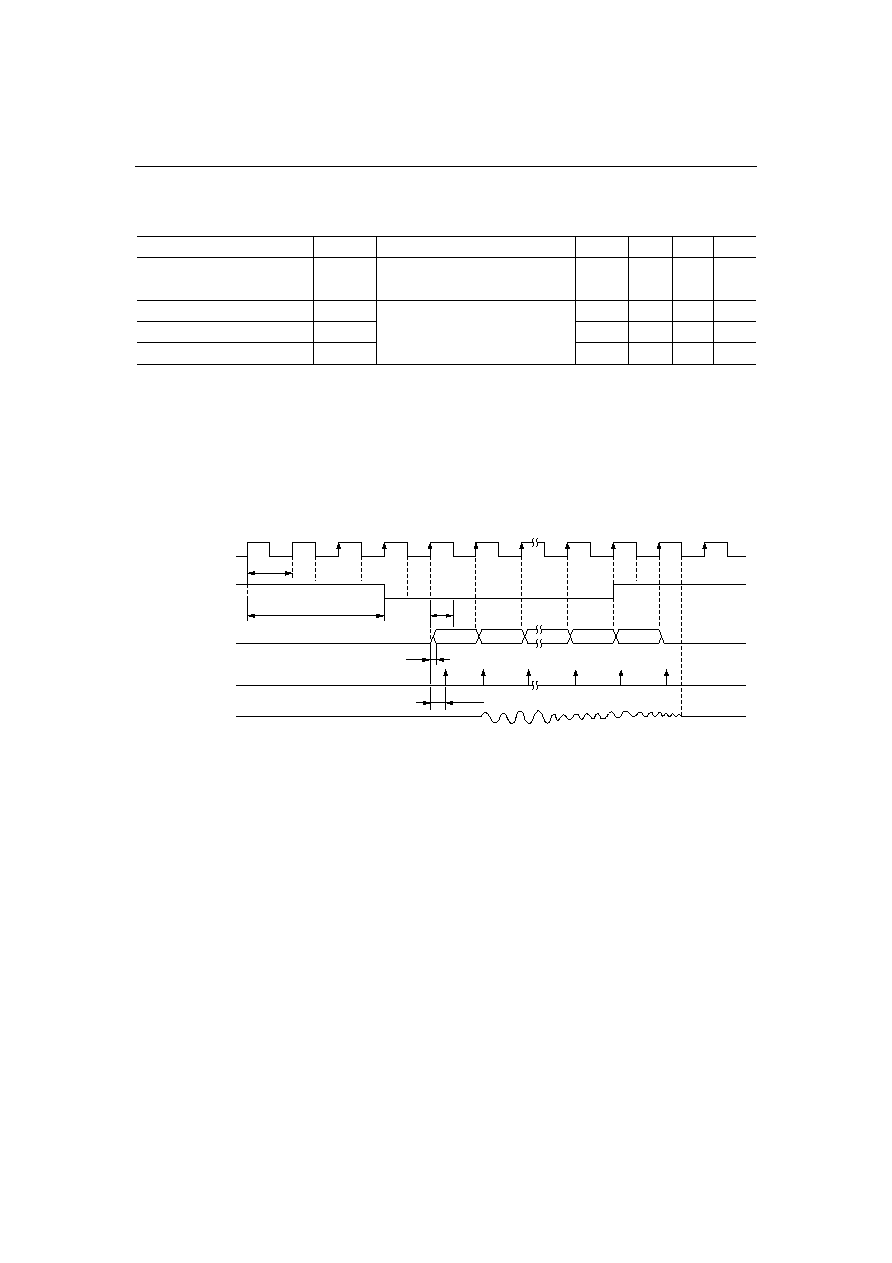
TIMING DIAGRAM
The VCK clock rising and falling edges are reversed between the MSM5205 and the MSM6588, as
indicated in DIFFERENCES BETWEEN MSM6585 AND MSM5205.
Note that the MSM6585 cannot accept data if the MSM5205 controls to repeat valid and invalid each
half cycle, when the MSM5205 is replaced with the MSM6585.
t
VCK
t
W(RST)
t
H
t
S
t
VCK/8
VCK (O)
RESET (I)
D3 - D0 (I)
IC internalD3 - D0
selection timings
AOUT, DAO (O)
ADPCM1 ADPCM2
ADPCMN
ADPCM
N+1
° Semiconductor
7
MSM6585
FUNCTIONAL DESCRIPTION
1.
Sampling Frequency
The relationship of the sampling frequencies on S1 and S2, and the cutoff frequencies are
listed below.
Cutoff frequency (f
CUT
)
1.6 kHz
3.2 kHz
6.4 kHz
12.8 kHz
Sampling frequency (f
SAM
)
4 kHz
8 kHz
16 kHz
32 kHz
S2
L
L
H
H
S1
L
H
L
H
2.
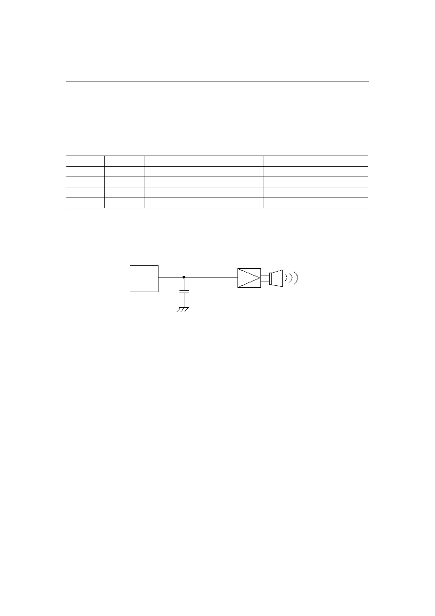
AOUT Connecting Circuit
Connect a 0.01mF capacitor to the AOUT pin. The circuit diagram is as shown below.
AOUT
0.01mF
MSM6585
Amplifier
Speaker
Even when the DAO pin is used, connect a 0.01mF capacitor to the AOUT pin. This capacitor is used
for the improvement of a voice quality.
3.
Voice Output
The MSM6585 has two voice output pins. The DAO is direct output pin from the internal DA
converter. The AOUT is a pin to output a voice after which the DAO output passed a built-in LPF.
3.1
DA Converter Output Waveform
The output amplitude from the DA converter is max. (4095/4096) • V
DD
and becomes a stair step
waveform synchronized with the sampling frequency. The DAO output impedance varies in the
ranges from 10kW to 40kW. Therefore, determine the filter constant so that the resistor variation does
not have influence on the cutoff frequency of the filter.
° Semiconductor
8
MSM6585
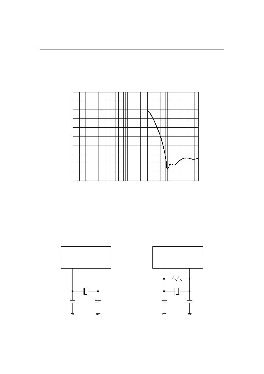
3.2
Low-pass Filter Output
The cutoff frequency of the low-pass filter varies in proportion to the sampling frequency.
The following figure shows the low-pass filter characteristics in the sampling frequency
8kHz.
4.
Oscillation
Following show external circuit diagrams using a ceramic resonator, KBR-640B made by
Kyocera Corp. and CSB640P made by Murata MFG. Co., Ltd.
0
≠20
≠40
≠60
100
1k
10k
Frequency (Hz)
Damping factor (dB)
XT
XT
640kHz
220pF
MSM6585
220pF
Kyocera Corp.
KBR-640B used
XT
XT
640kHz
100pF
MSM6585
100pF
Murata MFG. Corp.
CSB640P used
1MW
° Semiconductor
9
MSM6585
APPLICATION CIRCUITS
Centronics Interface Circuit (sampling frequency : 8kHz)
BUSY
STROBE
RESET
D0
D1
D2
D3
D4
D5
D6
D7
0.1mF
7
5
3
1
6
4
2
15
9
8
14
16
13
12
11
10
12
9 13
14
4
1
6
3
5
8
7
10
2
11
S1
AOUT
640kHz
D1 D0
0.01mF
AMP
MSM6585
ADPCM
DECODER
MSM4013
MSM4019
+5V
0.1mF
0.1mF
T3
V
DD
DAO
XT
XT
D2
D3
RESET
VCK
T4
T1
S2
GND
T2
Centronics Timing Chart
RESET
RES
DATA
STROBE
VCK
KA
KB
BUSY
MIN250msec
125msec
First byte
High nibble
Low nibble
° Semiconductor
10
MSM6585
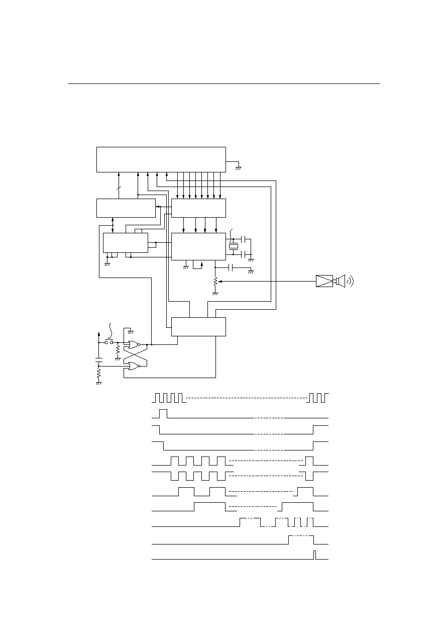
Example of Interface Circuit with 256K-bit EPROM
The circuit example and timing diagram that used the 256K-bit EPROM are shown below.
MSM27256
CE
A0 - A10
A11 A12 A13 A14
O0 O4 O1 O5 O2 O6 O3 O7
O0 - O11
O12
CL
B1 A1
RESET
B2 A2 B3
B4
A3
A4
KB
MSM4019
KA D1
D2 D3
D4
S1
Q2 D2 Q2
CL1
CL2
MSM4013
R1D1S2 Q1R2
D0
D1 D2
D3
XT
XT
MSM6585
RESET S2 S1
AOUT
640kHz
0.01mF
100kW
Q1
Q2 Q3
MSM4040
RESET
Q4
START SW
10kW
0.1mF
100kW
(MSM4025)
11
M6585 VCK (O)
START SW
M4013 S1
M4013 Q1
M4013 Q2
Q2
M4040 Q1
Q2
Q12
M4040 Q3
Q4
CL
(M6585 RESET)
(Lower 4-bit)
(Upper 4-bit)
VCK
MSM4040
° Semiconductor
11
MSM6585
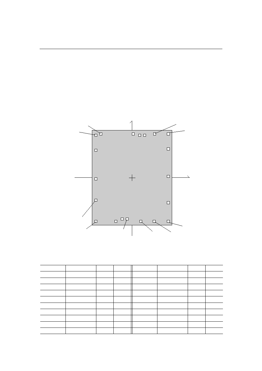
PAD CONFIGURATION
Pad Layout
Product name
MSM6585
Function
ADPCM voice synthesis IC
Die size
• = 2.92 mm, Y = 3.58 mm
Die thickness
350
µ
m
±
30
µ
m
Pad size
130
µ
m • 130
µ
m
Substrate voltage
GND
Y
X
8
7
3
2
1
20
17
16
13
12
Pad Coordiantes
(The die center is located at X=0, Y=0)
PAD No.
PAD Name
X-axis
Y-axis
PAD No.
PAD Name
X-axis
Y-axis
1
S1
377
≠1635
11
AOUT
38
1635
2
S2
819
≠1635
12
DAO
≠1125
1635
3
T3
1305
≠1635
13
T1
≠1305
1579
4
D0
1305
≠943
14
T2
≠1305
1009
5
D1
1305
44
15
VCK
≠1305
≠88
6
D2
1305
1095
16
RESET
≠1305
≠818
7
D3
1305
1635
17
XT
≠1281
≠1635
8
T4
830
1635
18
XT
≠529
≠1635
9
AV
SS
447
1580
19
V
DD
≠299
≠1549
(Unit: mm)
10
V
SS
267
1580
20
AV
DD
≠119
≠1549
° Semiconductor
12
MSM6585
(Unit : mm)
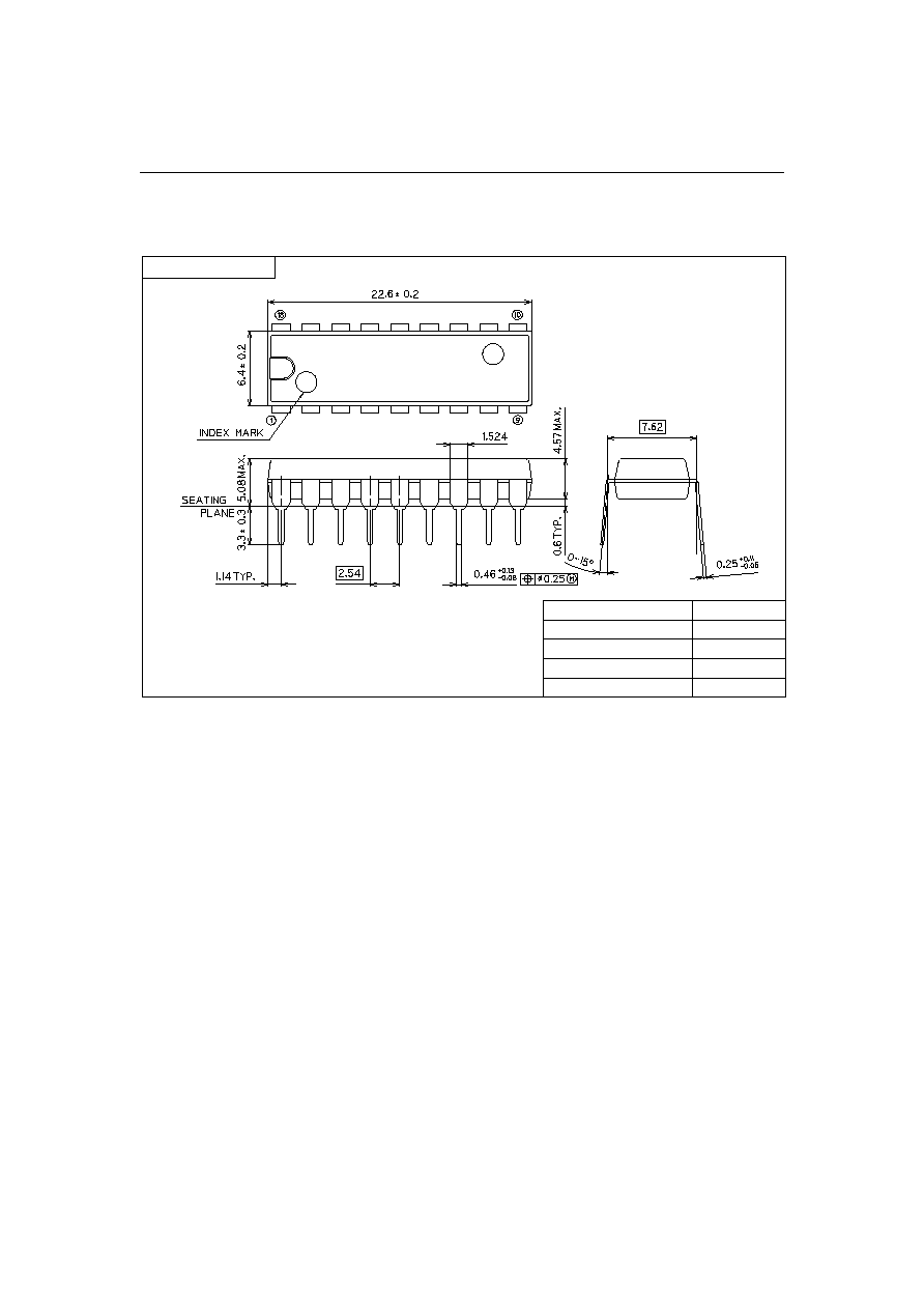
PACKAGE DIMENSIONS
DIP18-P-300-2.54
Package material
Lead frame material
Pin treatment
Solder plate thickness
Package weight (g)
Epoxy resin
42 alloy
Solder plating
5 mm or more
1.30 TYP.
° Semiconductor
13
MSM6585
(Unit : mm)
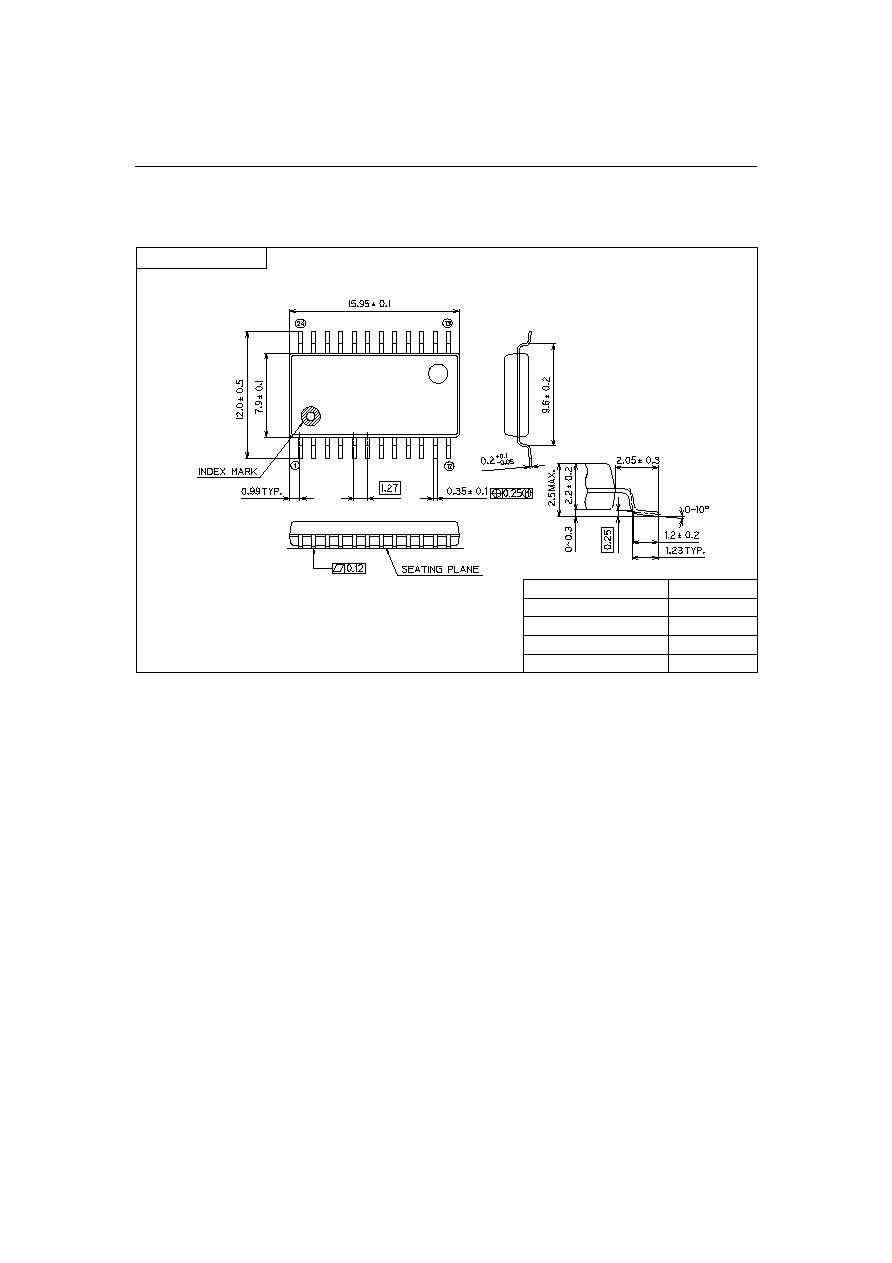
Notes for Mounting the Surface Mount Type Package
The SOP, QFP, TSOP, TQFP, LQFP, SOJ, QFJ (PLCC), SHP, and BGA are surface mount type
packages, which are very susceptible to heat in reflow mounting and humidity absorbed in
storage. Therefore, before you perform reflow mounting, contact Oki's responsible sales person
on the product name, package name, pin number, package code and desired mounting conditions
(reflow method, temperature and times).
SOP24-P-430-1.27-K
Package material
Lead frame material
Pin treatment
Solder plate thickness
Package weight (g)
Epoxy resin
42 alloy
Solder plating
5 mm or more
0.58 TYP.
Mirror finish
° Semiconductor
14
MSM6585
(Unit : mm)
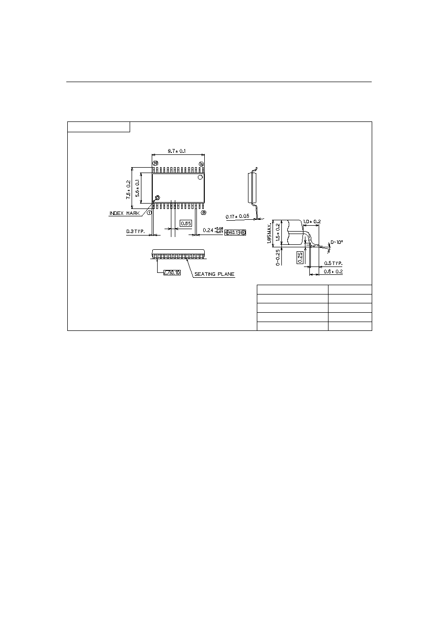
Notes for Mounting the Surface Mount Type Package
The SOP, QFP, TSOP, TQFP, LQFP, SOJ, QFJ (PLCC), SHP, and BGA are surface mount type
packages, which are very susceptible to heat in reflow mounting and humidity absorbed in
storage. Therefore, before you perform reflow mounting, contact Oki's responsible sales person
on the product name, package name, pin number, package code and desired mounting conditions
(reflow method, temperature and times).
SSOP30-P-56-0.65-K
Package material
Lead frame material
Pin treatment
Solder plate thickness
Package weight (g)
Epoxy resin
42 alloy
Solder plating
5 mm or more
0.19 TYP.
Mirror finish
1Semiconductor
MSM6585
15
REVISION HISTORY
Page
Document
No.
Date
Previous
Edition
Current
Edition
Description
E2D0011-39-91
Sep. 1999
--
--
Final edition 1
--
--
Final edition 2
1 1
Changed the voice analysis editing tools from
AR203 and AR204 to AR207.
FEDL6585-02
Jun. 30, 2004
1 1
Changed the package product names from
MSM6585GS-K and MSM6585GS-AK to
MSM6585MAZXXX and MSM6585MBZXXX,
respectively.
FEDL6585-03
Aug. 25, 2004
10 10
Changed the product name of the circuit block in
the upper-left portion of the block diagram from
MSM4013 to MSM4040.

1Semiconductor
MSM6585
16
NOTICE
1. The information contained herein can change without notice owing to product and/or technical
improvements. Before using the product, please make sure that the information being referred to is
up-to-date.
2. The outline of action and examples for application circuits described herein have been chosen as an
explanation for the standard action and performance of the product. When planning to use the product,
please ensure that the external conditions are reflected in the actual circuit, assembly, and program designs.
3.
When designing your product, please use our product below the specified maximum ratings and within the
specified operating ranges including, but not limited to, operating voltage, power dissipation, and operating
temperature.
4. Oki assumes no responsibility or liability whatsoever for any failure or unusual or unexpected operation
resulting from misuse, neglect, improper installation, repair, alteration or accident, improper handling, or
unusual physical or electrical stress including, but not limited to, exposure to parameters beyond the
specified maximum ratings or operation outside the specified operating range.
5. Neither indemnity against nor license of a third party's industrial and intellectual property right, etc. is
granted by us in connection with the use of the product and/or the information and drawings contained
herein. No responsibility is assumed by us for any infringement of a third party's right which may result
from the use thereof.
6. The products listed in this document are intended for use in general electronics equipment for commercial
applications (e.g., office automation, communication equipment, measurement equipment, consumer
electronics, etc.). These products are not, unless specifically authorized by Oki, authorized for use in any
system or application that requires special or enhanced quality and reliability characteristics nor in any
system or application where the failure of such system or application may result in the loss or damage of
property, or death or injury to humans.
Such applications include, but are not limited to, traffic and automotive equipment, safety devices,
aerospace equipment, nuclear power control, medical equipment, and life-support systems.
7.
Certain products in this document may need government approval before they can be exported to particular
countries. The purchaser assumes the responsibility of determining the legality of export of these products
and will take appropriate and necessary steps at their own expense for these.
8. No part of the contents contained herein may be reprinted or reproduced without our prior permission.
Copyright 2004 Oki Electric Industry Co., Ltd.