1/9
° Semiconductor
MSM6597A-xxx
° Semiconductor
MSM6597A-xxx
3-Mbit Serial Voice ROM
GENERAL DESCRIPTION
The MSM6597A is a MSM6597 short TAT process version.
The MSM6597A is a serial voice ROM with a 1,048,576-word • 1-bit • 3-bank configuration.
The MSM6597A has a built-in internal address-generating circuit. A single, external clock input
allows continuous, serial read operations. The internal addresses are automatically incremented
by 1 by read operation. 1024 words in X direction and 1024 words in Y direction can be addressed
by inputting external serial addresses. Banks are switched with CS1, CS2, and CS3.
A read and playback device with predetermined messages can easily be configured by storing voice
data into the MSM6597A and by combining it with one of Oki's recording and playback ICs and with
one of Oki's serial registers.
A serial register is required to drive the MSM6597A when used with the MSM6388 or MSM6588. (The
MSM6597A does not operate without a serial register.)
The major differences between the MSM6597A and MSM6597 are shown below.
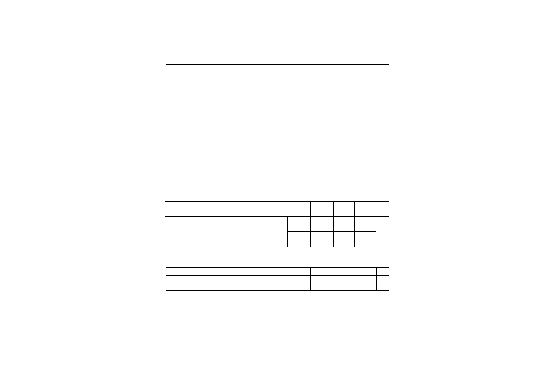
MSM6597A DC Characteristics
Parameter
Symbol
Condition
Min.
Max.
Unit
V
DD
= 3.5 to 5.5 V, Ta = ≠40 to +85∞C
Current Consumption (1)
I
DD
t
RDC
= 2.5 ms
--
20
mA
Current Consumption (2)
I
DS
CS1
= CS2
= CS3
= V
DD
≠ 0.2 V
Ta = ≠40
to +70∞C
10
mA
Typ.
9
--
Ta = ≠40
to +85∞C
50
--
--
--
MSM6597 DC Characteristics
For other detailes, refer to individual sections in this data sheet.
FEATURES
∑ Configuration
:
1,048,576 words • 1 bit • 3 banks
∑ Serial access
:
Read cycle time of 2.5 ms
∑ Shorter-TAT processing
∑ Power-supply voltage
:
5 V single supply
∑ Package options :
24-pin plastic SOP (SOP24-P-430-1.27-K) (Product name : MSM6597A-xxxGS-K)
30-pin plastic SSOP (SSOP30-P-56-0.65-K) (Product name : MSM6597A-xxxGS-AK)
E2D0040-39-22
Parameter
Symbol
Condition
Min.
Max.
Unit
Current Consumption (1)
I
DD
t
RDC
= 2.5 ms
--
15
mA
Typ.
--
Current Consumption (2)
I
DS
CS1
= CS2
= CS3
= V
DD
≠ 0.2 V
--
10
mA
--
Typical values are at V
DD
= 5.0 V, Ta = 25∞C
V
DD
= 3.5 to 5.5 V, Ta = ≠40 to +85C∞
This version: Feb. 1999
Previous version: May. 1997
2/9
° Semiconductor
MSM6597A-xxx
SADY
SASY
CS2
CS1
NC
NC
NC
NC
SADX
SASX
TAS
V
DD
GND
CS3
DOUT
TESTO1
NC
NC
NC
NC
NC
RDCK
TESTO2
TEST
1
2
3
4
5
6
7
8
9
10
11
12
24
23
22
21
20
19
18
17
16
15
14
13
NC : No connection
24-Pin Plastic SOP
NC : No connection
30-Pin Plastic SSOP
SADY
SASY
CS2
NC
CS1
NC
NC
NC
NC
NC
NC
SADX
SASX
TAS
V
DD
GND
CS3
DOUT
TESTO1
NC
NC
NC
NC
NC
NC
NC
NC
RDCK
TESTO2
TEST
1
2
3
4
5
6
7
8
9
10
11
12
13
14
15
30
29
28
27
26
25
24
23
22
21
20
19
18
17
16
BLOCK DIAGRAM
PIN CONFIGURATION (TOP VIEW)
SADX
SASX
SADY
SASY
TAS
RDCK
CS2
CS1
X-ADDRESS
REGISTER
Sin
CK
Y-ADDRESS
REGISTER
Sin
CK
X-ADDRESS
COUNTER
LD
Y-ADDRESS
COUNTER
LD
CK
CK
10
10
X-DECODER
Y-DECODER
Memory Cell
Matrix
393216 x 8
MULTIPLEXER
V
DD
GND
TEST
TESTO1
TESTO2
DOUT
10
1
2
6
3
MULTIPLEXER
CS3
CS CONTROLLER
3/9
° Semiconductor
MSM6597A-xxx
PIN DESCRIPTIONS
Type
Description
--
Power supply pin. Insert a bypass capacitor of 0.1 mF or more between this pin and the
GND pin.
--
Ground pin
I
(SERIAL ADDRESS) This pin inputs the starting X address of a read operation.
Addressing in units of 1024 words is possible. The 1024-word address data can be
input as 10-bit (AX0 - AX9) serial data via the SADX pin.
I
I
(SERIAL ADDRESS STROBE) This is the clock input pin which is used to store the
serial address data of the X address into the device's internal register.
(SERIAL ADDRESS STROBE) This is the clock input pin which is used to store the
serial address data of the Y address into the device's internal register.
I
(ADDRESS TRANSFER STROBE) This is the input pin for loading the serial address
data into the internal address counter.
The X and Y addresses are stored at the falling edge of TAS.
Symbol
V
DD
GND
SADX
SADY
SASX
TAS
(SERIAL ADDRESS) This pin inputs the starting Y address of a read operation.
Addressing in units of 1024 words is possible. The 1024-word address data can be
input as 10-bit (AY0 - AY9) serial data via the SADY pin.
I
SASY
I
(READ CLOCK) This is the clock input pin for reading information out of the data
register. Internal operation starts at the falling edge of RDCK. The information in the
data register is output on the DOUT pin. The internal address counter is automatically
incremented by 1 at the falling edge of RDCK.
RDCK
O
(DATA OUT) The data output pin is always kept in a high-impedance state when CS1,
CS2, and CS3 are all kept "H" or when RDCK is kept "H". This pin reflects the "H" or "L"
level data being read, and the current data is hold until RDCH is asserted High.
DOUT
I
(CHIP SELECT) When either CS1, CS2, or CS3 is "L", bank 1, bank 2, or bank 3 is
selected, respectively. Setting all three signals "H" disables all input and output
pins. These pins enable parallel use of multiple serial voice ROMs by connecting the
data output pins.
CS1
I
Pin for testing. Apply "L" level.
TEST
O
Pins for testing. Leave these pins open.
TESTO1
SSOP
SOP
15
12
30
24
12
9
1
1
13
10
2
2
14
11
18
15
28
22
CS2
CS3
5
3
29
4
3
23
TESTO2
16
13
27
21
17
14
Pin
ABSOLUTE MAXIMUM RATINGS
Parameter
Symbol
Condition
Rating
Unit
Power Supply Voltage
V
DD
Ta = 25∞C
≠0.3 to +7.0
V
Input Voltage
V
IN
Ta = 25∞C
≠0.3 to V
DD
+0.3
V
Storage Temperature
T
STG
--
≠55 to +150
∞C
4/9
° Semiconductor
MSM6597A-xxx
RECOMMENDED OPERATING CONDITIONS
ELECTRICAL CHARACTERISTICS
DC Characteristics
Parameter
Symbol
Condition
Range
Unit
Power Supply Voltage
V
DD
GND=0V
3.5 to 5.5
V
Operating Temperature
T
op
--
≠40 to +85
∞C
Parameter
Symbol
Condition
Min.
Max.
Unit
V
DD
= 3.5 to 5.5 V, Ta = ≠40 to +85∞C
"H" Level Input Voltage
V
IH
--
0.8xV
DD
--
V
"L" Level Input Voltage
V
IL
--
--
0.8
V
"H" Level Output Voltage
V
OH
I
OH
= ≠40 mA
V
DD
≠0.3
--
V
"L" Level Output Voltage
V
OL
I
OL
= 2 mA
--
0.45
V
"H" Level Input Current
I
IH
V
IH
= V
DD
--
10
mA
"L" Level Input Current
I
IL
V
IL
= GND
≠10
--
mA
Current Consumption (1)
I
DD
t
RDC
= 2.5 ms
--
20
mA
Current Consumption (2)
I
DS
CS1
= CS2
= CS3
= V
DD
≠ 0.2 V
Ta = ≠40
to +70∞C
10
mA
Typ.
--
--
--
--
--
--
9
--
Ta = ≠40
to +85∞C
50
--
--
--
Typical values are at V
DD
= 5.0 V, Ta = 25
∞
C
AC Characteristics
Parameter
Symbol
Min.
Max.
Unit
V
DD
= 3.5 to 5.5 V, Ta = ≠40 to +85∞C
CS, SAS Setup Time
t
CSS
1000
--
ns
SASX, SASY Cycle Time
t
SSC
500
--
ns
SASX, SASY Precharge Time
t
SAP
250
--
ns
SASX, SASY Pulse Width
t
SAS
250
--
ns
Address Setup Time
t
AS
100
--
ns
Address Hold Time
t
AH
100
--
ns
TAS Setup Time
t
ATS
500
--
ns
TAS, RDCK Setup Time
t
TRS
500
--
ns
TAS Pulse Width
t
TAS
250
--
ns
Read Cycle Time
t
RDC
2500
--
ns
Access Time
t
ACC
--
1500
ns
Output Turn-off Delay Time
t
OFF
0
200
ns
RDCK Precharge Time
t
RDP
1000
--
ns
RDCK Pulse Width
t
RD
1500
--
ns
5/9
° Semiconductor
MSM6597A-xxx
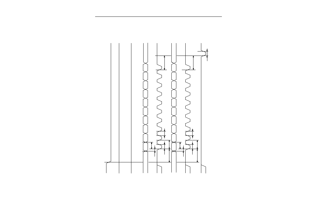
TIMING DIAGRAMS
Serial Address Input Timing
,
,
CS2 (I)
SADX (I)
SASX (I)
SADY (I)
t
AH
TAS (I)
SASY (I)
AX1
AX2
AX3
AX4
AX5
AX6
AX7
AX8
AX9
t
AS
t
SAS
t
CSS
t
SSC
t
SAP
t
ATS
t
ATS
t
TAS
t
AS
t
AH
t
SAS
t
SAP
t
SSC
t
CSS
AX0
AY0
AY1
AY2
AY3
AY4
AY5
AY6
AY7
AY8
AY9
,
,
,
,
,
,
,
,
CS3 (I)
CS1 (I)