
1/22
° Semiconductor
MSM65522/65P522
GENERAL DESCRIPTION
The MSM65522 is a high-performance 8-bit microcontroller that employs OKI original nX-8/50
CPU core. With a minimum instruction execution time of 400 ns (10MHz clock), the MSM65522
is capable of high-speed processing, and includes 8K bytes of program memory, 384 bytes of
data memory (RAM), timers, serial ports and an A/D converter on chip. Also available is the
MSM65P522, which replaces the on-chip program memory with one-time PROM.
FEATURES
∑ Operating range
Operating frequency
: 1 to 10MHz (V
DD
=4.5 to 5.5V)
1 to 5MHz (V
DD
=2.7 to 5.5V)
Operating voltage
: 2.7 to 5.5V
Operating temperature
: ≠ 40 to +85
∞
C
∑ Memory space
Internal program memory
: 8K bytes
Internal data memory
: 384 bytes
∑ Minimum instruction execution time
: 400ns @ 10 MHz
∑ Powerful instruction set
: 81 basic instructions
8/16-bit operation instructions
Bit manipulation instructions
Compound function instructions
∑ Abundant addressing modes
∑ I/O ports
: 8-bit • 3
4-bit • 1
Input only port
: 8-bit • 1
∑ Timers
: 8-bit auto-reload timer • 3
(One timer is shared by the baud rate
generator. Combining the 8-bit timers,
it is possible to use the timers as a 16-bit
timer (1 channel).)
Watchdog timer • 1
∑ Counters
: Time base counter (14-bit) • 1
∑ Serial ports
: Shift register • 1
Serial port with baud rate generator
(UART/Synchronous) • 1
∑ A/D converter
: 8 bits • 8 channels
∑ External interrupts
: 3
∑ Interrupt sources
: 11
∑ Package Options
42-pin plastic shrink DIP (SDIP42-P-600-1.78)
: (Product name:MSM65522-•••SS,
MSM65P522-•••SS)
42-pin plastic DIP (DIP42-P-600-2.54)
: (Product name:MSM65522-•••RS,
MSM65P522-•••RS)
44-pin plastic QFP (QFP44-P-910-0.80-2K)
: (Product name:MSM65522-•••GS-2K,
MSM65P522-•••GS-2K)
44-pin plastic QFJ (QFJ44-P-S650-1.27)
: (Product name:MSM65522-•••JS,
MSM65P522-•••JS)
••• indicates the code number.
* Specifications are subject to change without notice.
° Semiconductor
MSM65522/65P522
8-Bit Microcontroller with A/D Converter
E2E1015-27-Y4
This version: Jan. 1998
Previous version: Nov. 1996
2/22
° Semiconductor
MSM65522/65P522
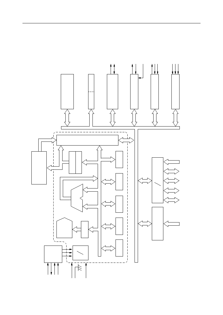
BLOCK DIAGRAM
OSC.
CONT.
CPU CORE
ROM
(8K bytes)
INST.
DEC.
T
C
IR
ALU
GMAR
BUS
CONT.
AR
BR
PSW
SP
LMAR
RAM
(384bytes)
TBC
WDT
SIO
8bit TIMER•3**
8bit SHIFT-REG.
INTERRUPT CONT.
8bit ADC
•8ch
I
O PORT
OSC0
OSC1
RESET
HSTOP*
V
DD
GND
TEST
8
8
AI0*
to
AI7*
PO
P1
P2
P3
P6
* Indicates the secondary function of the port.
** One of the asterisked items is used in the SIO baud rate generator.
TXD*
RXD*
T1OUT*
T0CK*
GATE*
SFTO*
SFTI*
SFTCK*
INT0*
INT1*
INT2*
PC
8
3/22
° Semiconductor
MSM65522/65P522
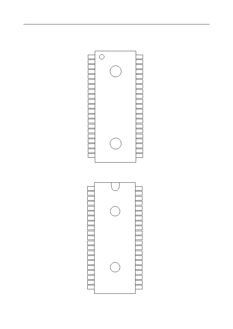
PIN CONFIGURATION (TOP VIEW)
42-Pin Plastic Shrink DIP
42-Pin Plastic DIP
P3.0
1
P3.1
2
P3.2
3
P3.3
4
P3.4 / INT2
5
P3.5 / SFT0
6
P3.6 / SFTI
7
P3.7 / SFTCK
8
RESET
9
P2.0 / RXD
10
P2.1 / TXD
11
P2.2 / INT0
12
P2.3 / INT1/ GATE
13
P2.4 / TOCK
14
P2.5 / HSTOP
15
P2.6
16
P2.7 / T1OUT
17
P1.3
18
OSC1
19
OSC0
20
GND
21
42
41
40
39
38
37
36
35
34
33
32
31
30
29
28
27
26
25
24
23
22
V
DD
P6.0 / AI0
P6.1 / AI1
P6.2 / AI2
P6.3 / AI3
P6.4 / AI4
P6.5 / AI5
P6.6 / AI6
P6.7 / AI7
TEST
P0.0
P0.1
P0.2
P0.3
P0.4
P0.5
P0.6
P0.7
P1.0
P1.1
P1.2
P3.0
1
P3.1
2
P3.2
3
P3.3
4
P3.4 / INT2
5
P3.5 / SFT0
6
P3.6 / SFTI
7
P3.7 / SFTCK
8
RESET
9
P2.0 / RXD
10
P2.1 / TXD
11
P2.2 / INT0
12
P2.3 / INT1/ GATE
13
P2.4 / TOCK
14
P2.5 / HSTOP
15
P2.6
16
P2.7 / T1OUT
17
18
OSC1
19
OSC0
20
GND
40
39
38
37
36
35
34
33
32
31
30
29
28
27
26
25
24
23
V
DD
P6.0 / AI0
P6.1 / AI1
P6.2 / AI2
P6.3 / AI3
P6.4 / AI4
P6.5 / AI5
P6.6 / AI6
P6.7 / AI7
TEST
P0.0
P0.1
P0.2
P0.3
P0.4
P0.5
P0.6
P0.7
P1.0
P1.1
21
22
P1.2
P1.3
41
42
4/22
° Semiconductor
MSM65522/65P522
PIN CONFIGURATION (TOP VIEW) (Continued)
NC: No-connection pin
44-Pin Plastic QFP
34
35
36
37
38
39
40
41
42
43
44
22
21
20
19
18
17
16
15
14
13
12
33
32
31
30
29
28
27
26
25
24
23
1
2
3
4
5
6
7
8
9
10
11
P6.0 / AI0
P6.1 / AI1
P6.2 / AI2
P6.3 / AI3
V
DD
GND
P3.0
P3.1
P3.2
P3.3
P3.4 / INT2
P0.6
P0.7
P1.0
P1.1
P1.2
GND
NC
OSC0
OSC1
P1.3
P2.7 / T1OUT
P3.5 / SFT0
P3.6 / SFTI
P3.7 / SFTCK
RESET
P2.0 / RXD
P2.1 / TXD
P2.2 / INT0
P2.3 / INT1/ GATE
P2.4 / TOCK
P2.5 / HSTOP
P6.4 / AI4
P6.5 / AI5
P6.6 / AI6
P6.7 / AI7
TEST
P0.0
P0.1
P0.2
P2.6
P0.3
P0.4
P0.5
5/22
° Semiconductor
MSM65522/65P522
NC: No-connection pin
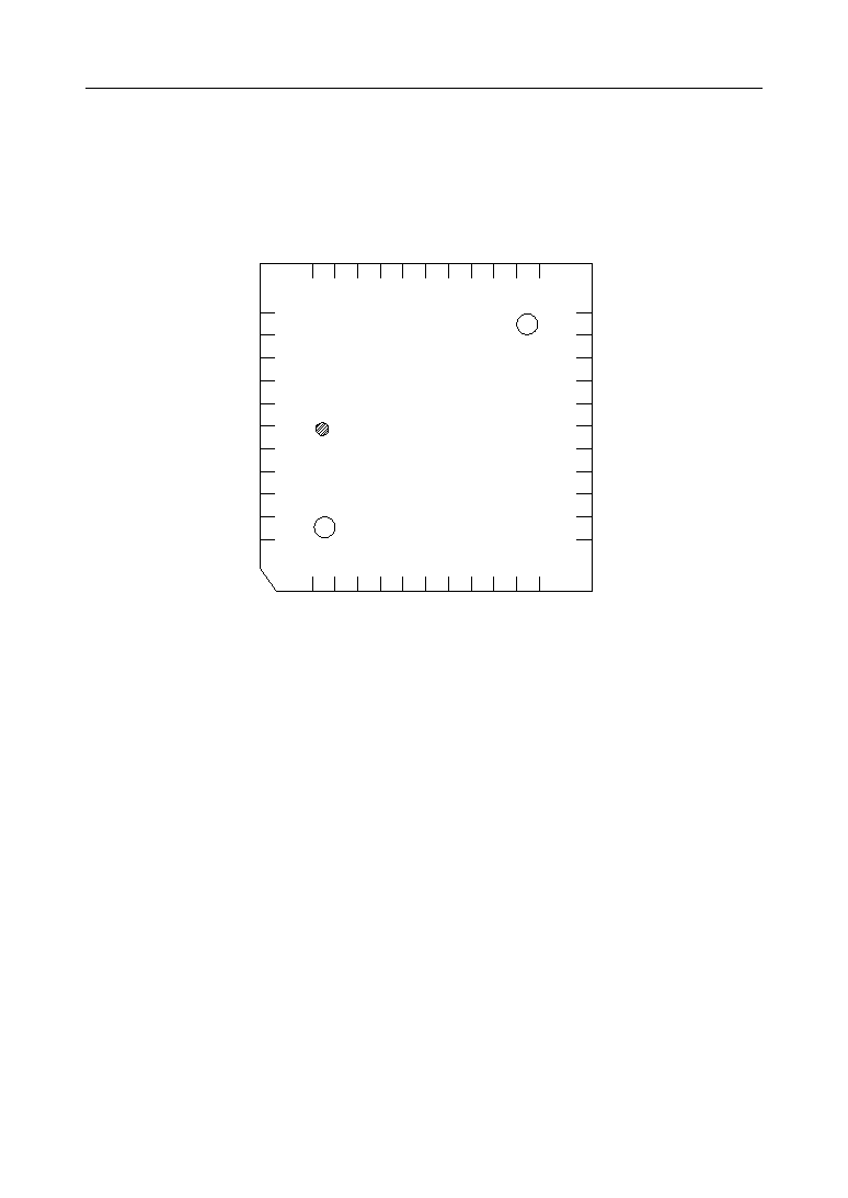
44-Pin Plastic QFJ
PIN CONFIGURATION (TOP VIEW) (Continued)
28
27
26
25
24
23
22
21
20
19
18
7
8
9
10 11 12 13 14 15 16 17
P6.0 / AI0
P6.1 / AI1
P6.2 / AI2
P6.3 / AI3
V
DD
P3.0
P3.1
P3.2
P3.3
P3.4 / INT2
P0.6
P0.7
P1.0
P1.1
P1.2
GND
OSC0
OSC1
P1.3
P2.7 / T1OUT
P3.5 / SFT0
P3.6 / SFTI
P3.7 / SFTCK
RESET
P2.0 / RXD
P2.1 / TXD
P2.2 / INT0
P2.3 / INT1/ GATE
P2.4 / TOCK
P2.5 /
HSTOP
P6.4 / AI4
P6.5 / AI5
P6.6 / AI6
P6.7 / AI7
TEST
P0.0
P0.1
P0.2
P2.6
P0.3
P0.4
P0.5
39 38 37 36 35 34 33 32 31 30 29
40
41
42
43
44
1
2
3
4
5
6
NC
NC
6/22
° Semiconductor
MSM65522/65P522
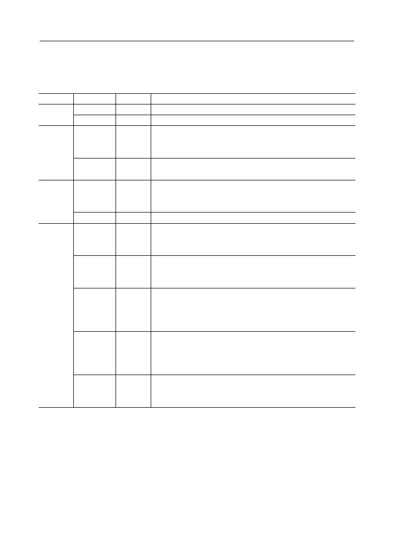
PIN DESCRIPTION
Basic Functions
Function
Symbol
Type
Description
Power
Supply
V
DD
--
+5V digital power supply (common to analog power supply)
GND
--
0V digital ground (common to analog ground)
OSC0
I
Oscillator input pin: connects to a crystal oscillator (or ceramic resonator)
or external clock. The master clock and external clock are used as the
system clock without frequency division.
OSC1
O
Oscillator input pin: connects to a crystal oscillator (or ceramic resonator).
When an external clock is input to OSC0, leave OSC1 open.
RESET
I
System reset input: when this pin goes low, the internal state of the chip
is initialized and program execution restarts from address 0040H. The
input is pulled up to V
DD
with an internal pull-up resistor.
Oscillation
TEST
I
Test input pin: connects to ground pin.
Control
P0.0
to
P0.7
I/O
8-bit input/output port (Port 0)
I/O
8-bit input/output port (Port 1)
I/O
8-bit input/output port (Port 2): input or output can be selected for each
bit by the port 2 direction register (P2DIR). In addition to their input/
output port functions, the pins of port 2 have secondary functions: see
the next table.
I/O
8-bit input/output port (Port 3): input or output can be selected for each
bit by the port 3 direction register (P3DIR). In addition to their input/
output port functions, the pins of port 3 have secondary functions: see
the next table.
I
8-bit input port (Port 6):
Functions as analog input channel during A/D conversion.
Port
P1.0
to
P1.3
P2.0
to
P2.7
P3.0
to
P3.7
P6.0/AI0
to
P6.7/AI7
7/22
° Semiconductor
MSM65522/65P522
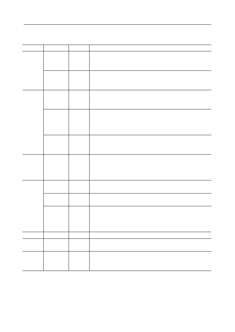
Secondary Functions
Function
Symbol
Type
Description
Serial
Port
RXD
I/O
P2.0 secondary functions.
UART: Input pin for a synchronous communication receive data.
Synchronous: Input/output pin for serial port transmit/receive data.
TXD
O
P2.1 secondary functions.
UART: Input pin for a synchronous communication receive data.
Synchronous: Output pin for serial port synchronizing clock.
External
interrupt
INT0
I
Secondary function of P2.2 input pin for external interrupt 0.
The interrupt can be triggered by the rising edge, falling edge, or both
edges of rising or falling.
INT1/Gate
I
Secondary function of P2.3 input pin for external interrupt 1.
The interrupt can be triggered by the rising edge, falling edge, or both
rising and falling edges. Also used as a gate signal input pin for gating
the counter of timer 0.
INT2
I
Secondary function of P3.4 input pin for external interrupt 2.
The interrupt can be triggered by the rising edge, falling edge, or both
rising and falling edges.
HSTOP
I
Secondary function of P2.0 input pin for hardware stop mode. If this pin goes
low while the HSTP bit in SBYCON is set to 1, the chip enters hard stop
mode. In hardware stop mode the clock stops and the CPU and on-chip
peripheral functions shut down to conserve power.
Control
SFTO
O
Shift
Registers
P3.5 secondary functions.
Shift register data output pin.
SFTI
I
P3.6 secondary functions.
Shift register data output pin.
SFTCK
I/O
P3.7 secondary functions.
Shift register synchronizing clock input/output pin.
In master mode: clock output
In slave mode: clock input
T0CK
I
Secondary function of P2.4: external clock input pin for timer 0.
Timer 0
T1OUT
O
Secondary function of P2.7: outputs a waveform with twice the cycle of
the overflow interval of timer 1.
Timer 1
AI0
to
AI7
O
Secondary function of P6.0 to P6.7: functions as analog input channel in
A/D conversion.
A/D
Converter
8/22
° Semiconductor
MSM65522/65P522
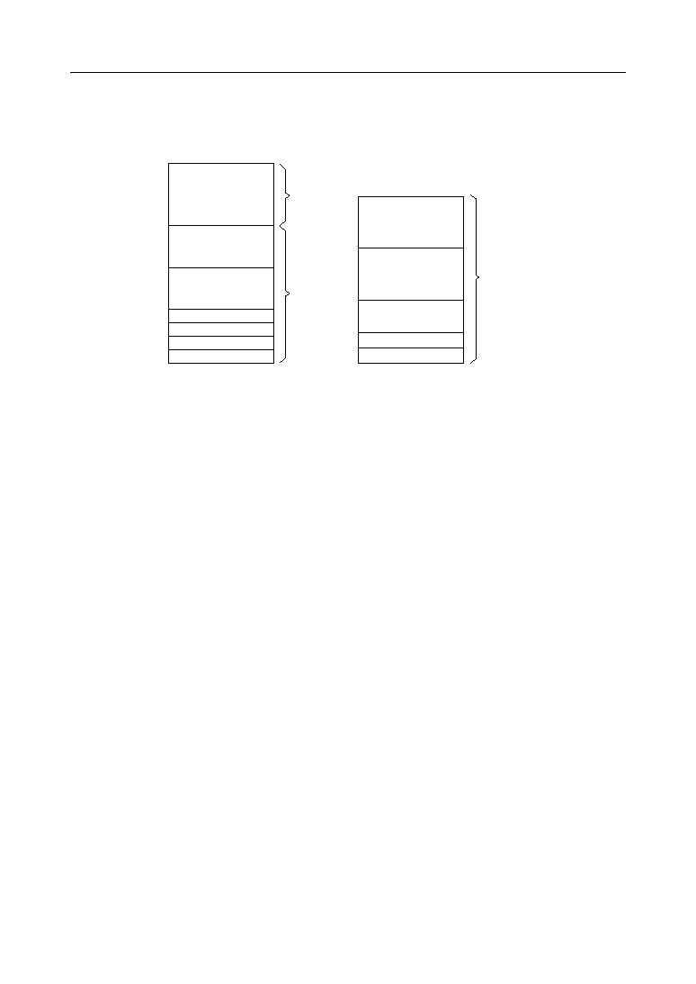
100H
80H
40H
30H
20H
10H
0
1FFFH
100H
80H
40H
20H
Internal Memory
Local Memory Space
SFR
Data Memory
Local Register Set 3
Local Register Set 2
Local Register Set 1
Local Register Set 0
General Memory Space
Program Memory
Vector Call Table Area
Program Memory
Interrupt Vector Table Area
Vector Call Table Area
0
1FFH
Data Memory
Page 1
Page 0
MEMORY MAPS
9/22
° Semiconductor
MSM65522/65P522
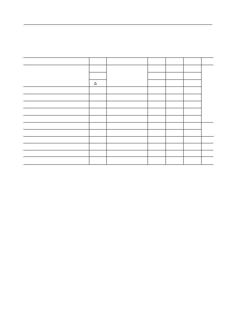
ABSOLUTE MAXIMUM RATINGS
Parameter
Unit
Supply Voltage
V
DD
≠0.3 to +7.0
Symbol
Condition
Rating
Ta=25∞C
Input Voltage
V
I
≠0.3 to V
DD
+0.3
Output Voltage
V
O
≠0.3 to V
DD
+0.3
Power Dissipation
P
D
400
Ta=25∞C per package
V
mW
Storage Temperature
T
STG
≠55 to +150
--
∞C
Analog Input Voltage
V
AI
≠0.3 to V
DD
+0.3
Ta=25∞C per one output
50
RECOMMENDED OPERATING CONDITIONS
Parameter
Unit
Supply Voltage
V
DD
4.5 to 5.5
Symbol
Condition
Range
f
OSC
£ 10 MHz
Memory Hold Voltage
V
DDMH
2.0 to 5.5
f
OSC
=0 Hz
Operating Frequency *
1
f
OSC
1 to 10
V
DD
=4.5 to 5.5
External Clock Operating
Frequency
f
EXTCLK
Operating Temperature
T
OP
≠40 to +85
--
V
MHz
MHz
∞C
Analog Input Voltage
V
AI
0 to V
DD
2.7 to 5.5
f
OSC
£ 5 MHz
--
1 to 5
V
DD
=2.7 to 4.5
0 to 10
V
DD
=4.5 to 5.5
0 to 5
V
DD
=2.7 to 4.5
*1 This is due to the standard of a crystal oscillator or resonator.
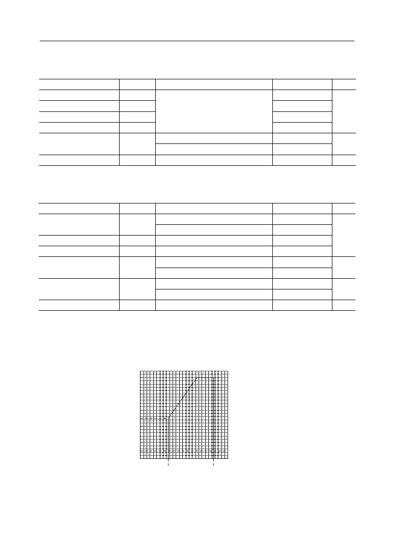
Figure 1. Supply Voltage vs. Operating frequency
2
5
4
6
8
10
2
3
4
5
6
1
2.7
5.5
Ta=≠40 to +85∞C
f
OSC
, f
EXTCLK
(MHz)
V
DD
(V)
* Operating Frequency is more than 1MHz.
10/22
° Semiconductor
MSM65522/65P522
ELECTRICAL CHARACTERISTICS
DC Characteristics 1 (V
DD
=4.5 to 5.5V, 5V Version)
(GND=0V, Ta=≠40 to +85∞C)
Parameter
Symbol
Condition
Min.
Typ.
Max.
Unit
"H" Input Voltage 1
V
IH1
--
0.3V
DD
+0.7
--
V
DD
+0.3
"H" Input Voltage 2
V
IH2
--
0.7V
DD
--
V
DD
+0.3
"L" Input Voltage
V
IL
--
≠0.3
--
0.3V
DD
-0.3
"H" Output Voltage 2
V
OH
I
OH
=≠400mA
V
DD
≠0.4V
--
--
"L" Output Voltage 1
V
OL
I
OL
=1.6mA
--
--
0.4
Input Leakage Current 1
I
LI1
V
I
=V
DD
/0V
--
--
±1
Input Leakage Current 2
I
LI2
V
I
=V
DD
/0V
--
--
±10
Current Consumption
I
DDS
5V, Stop mode
--
2
50
Current Consumption
I
DD
f
OSC
=10MHz, 5V, no load
--
25
35
V
m
A
m
A
mA
Schmitt Trigger Circuit
Input Voltage
V
T≠
0.3V
DD
--
--
V
T+
--
--
--
0.7V
DD
V
T
--
1.0
--
*
1
*
2
*
3
*
4
*
5
*
6
Input Capacitance
C
I
f=1MHz, Ta=25∞C
--
5
--
pF
*
8
Pull-up Resistor
R
RST
V
I
=0V
30
50
80
*
7
KW
*1 P0 to P3 (Includes secondary function inputs)
*2 P6
*3 OSC0 and RESET
*4 P6, OSC0, RESET
*5 P6
*6 Excludes P6. RESET sets to V
DD
and TEST sets to 0V
*7 RESET
*8 The ports set for input mode are V
DD
or 0V, the ports except these are no load and A/D
converter is not active.
11/22
° Semiconductor
MSM65522/65P522
DC Characteristics 2 (2.7 to 4.5V, 3V Version)
(GND=0V, Ta=≠40 to +85∞C)
Parameter
Symbol
Condition
Min.
Typ.
Max.
Unit
"H" Input Voltage
V
IH1
--
0.3V
DD
+0.7
--
V
DD
+0.3
"H" Input Voltage
V
IH2
--
0.7V
DD
+0.3
--
V
DD
+0.3
"L" Input Voltage
V
IL
--
≠0.3
--
0.3V
DD
≠0.3
"H" Output Voltage
V
OH
I
OH
=≠20mA
V
DD
≠0.1
--
--
"L" Output Voltage
V
OL
I
OL
=20mA
--
--
0.1
Input Leakage Current 1
I
LI1
V
I
=V
DD
/0V
--
--
±1
Input Capacitance
C
I
f=1MHz, Ta=25∞C
--
5
--
Current Consumption
I
DDS
3V, stop mode
1
--
25
Current Consumption
I
DD
5MHz, 3V, no load
10
6
15
V
m
A
pF
m
A
mA
*
2
Schmitt Trigger Circuit
Input Voltage
V
T≠
0.3V
DD
--
--
V
T+
--
--
--
0.7V
DD
V
T
--
0.5
--
*
1
*
3
*
4
*
5
Pull-up Resistor
R
RST
50
80
V
I
=0V
*
7
30
*
8
Input Leakage Current 1
I
LI1
V
I
=V
DD
/0V
--
--
±1
*
6
KW
*1 P0 to P3 (Includes secondary function inputs)
*2 P6
*3 OSC0 and RESET
*4 P6, OSC0, RESET
*5 P6
*6 Excludes P6. RESET sets to V
DD
and TEST sets to 0V.
*7 RESET
*8 The ports except these are no load, and A/D converter active.
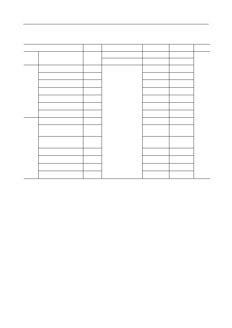
AC Characteristics
CPU control (OSC0 Clock)
Parameter
Symbol
Condition
Min.
Max.
Unit
Clock Period
"L" Clock Pulse Width
"H" Clock Pulse Width
Clock Period
"L" Clock Pulse Width
"H" Clock Pulse Width
t
C
t
CLW
t
CHW
t
C
t
CLW
t
CHW
100
45
45
200
90
90
--
--
--
--
--
--
ns
V
DD
=4.5 to 5.5 V
V
DD
=2.7 to 4.5 V
(V
DD
=2.7 to 5.5 V, GND=0V, Ta=≠40 to +85∞C)
CPU control (OSC0 Clock)
OSC0
t
C
t
CLW
t
CHW

12/22
° Semiconductor
MSM65522/65P522
Figure 2. Voltage vs. Current
10
20
30
40
50
2
3
4
5
6
I
DD
(mA)
V
DD
(V)
10
20
30
40
50
2
3
4
5
6
I
DD
(mA)
V
DD
(V)
10
20
30
40
50
2
3
4
5
6
I
DD
(mA)
V
DD
(V)
10MHz
Max.
Typ.
Max.
Typ.
Max.
Typ.
6MHz
2MHz
Ta=≠40 to +85∞C, no load
13/22
° Semiconductor
MSM65522/65P522
∑ CPU control
(V
DD
=2.7 to 5.5V, GND=0V, Ta=≠40 to +85∞C)
Parameter
Symbol
Condition
Min.
Max.
Unit
RESET Pulse Width
*1
t
RESW1
20
--
ns
RESET Pulse Width
*2
t
RESW2
*3
--
--
--
--
*1 Excluding power ON, stop mode and hard stop mode.
*2 In power ON, stop mode and hard stop mode.
*3 Oscillation stabilization time depends on resonator.
RESET Pulse Width
t
RESW1, 2
RESET
∑ Peripheral control 1
(V
DD
=2.7 to 5.5V, GND=0V, Ta=≠40 to +85∞C)
Parameter
Symbol
Condition
Min.
Max.
Unit
Clock Period
t
C
100
--
ns
External Interrupt Pulse
Width
t
EXIW
4 t
C
--
External Clock Pulse
Width
t
T0CW
4 t
C
--
GATE Pulse Width
t
T0GW
1 t
TOCLK
*1
--
--
OSC
EXI
T0
V
DD
=4.5 to 5.5V
V
DD
=2.7 to 4.5V
200
--
*1 t
T0CLK
: Timer 0 count clock period selected by T0CON.
14/22
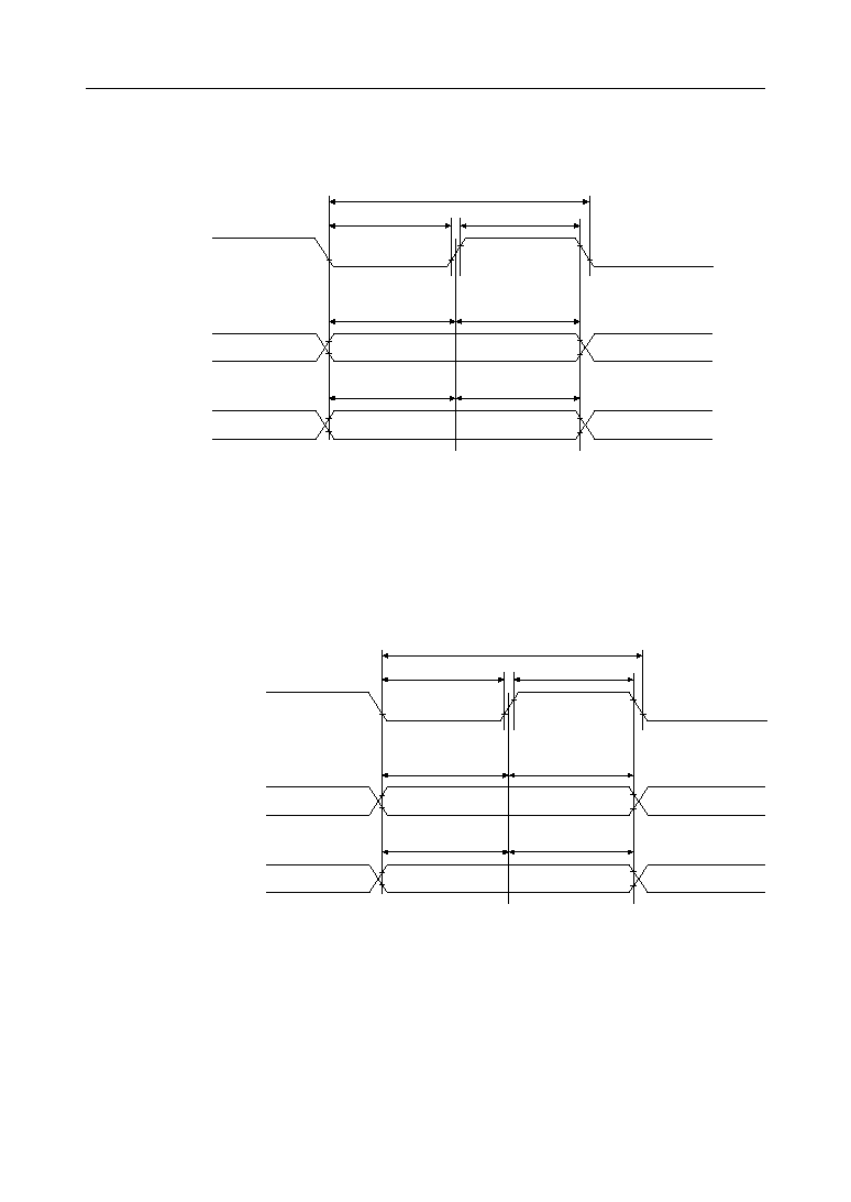
° Semiconductor
MSM65522/65P522
1) OSC0
OSC0
t
C
t
CLW
2) EXI Pulse Width
INT0-2
t
EXIW
3) T0
T0CK
t
T0CW
GATE
t
T0GW
15/22
° Semiconductor
MSM65522/65P522
(V
DD
=AV
DD
=2.7 to 5.5V, GND=0V, Ta=≠40 to +85∞C)
Parameter
Symbol
Condition
Min.
Max.
Unit
Clock Period
t
C
100
--
ns
SFTCK Period
t
SFC
8 t
C
--
SFTCK "L" Pulse Width
t
SFCLW
4 t
C
≠20
--
SFTCK "H" Pulse Width
t
SFCHW
4 t
C
≠20
--
OSC
SFT
SFTO Setup Time
t
SFOS
t
SFCLW
≠100
--
SFTO Hold Time
t
SFOH
t
SFCHW
≠100
--
SFTI Setup Time
t
SFIS
100
--
SFTI Hold Time
t
SFIH
100
--
C
L
=100pF
Synchronous Clock Period
t
SIC
8 t
C
--
Synchronous Clock "L"
Pulse Width
t
SICLW
4 t
C
≠20
--
Synchronous Clock "H"
Pulse Width
t
SICHW
4 t
C
≠20
--
Output Data Setup Time
t
SIOS
6 t
C
≠100
--
Output Data Hold Time
t
SIOH
2 t
C
≠100
--
Input Data Setup Time
t
SIIS
t
C
+t
CLW
+100
--
Input Data Hold Time
t
SIIH
0
--
SIO
(Clock
Synchro-
nous
Mode)
V
DD
=4.5 to 5.5V
200
--
V
DD
=2.7 to 4.5V
∑ Peripheral control 2
16/22
° Semiconductor
MSM65522/65P522
1) SFT
t
SFCLW
t
SFCHW
t
SFC
t
SFOS
t
SFOH
t
SFIS
t
SFIH
SFTCK
SFTO
SFTI
2) SIO
(Clock Synchronous Mode)
t
SICLW
t
SICHW
t
SIC
t
SIOS
t
SIOH
t
SIIS
t
SIIH
TXD
RXD (transmission)
RXD (reception)
17/22
° Semiconductor
MSM65522/65P522
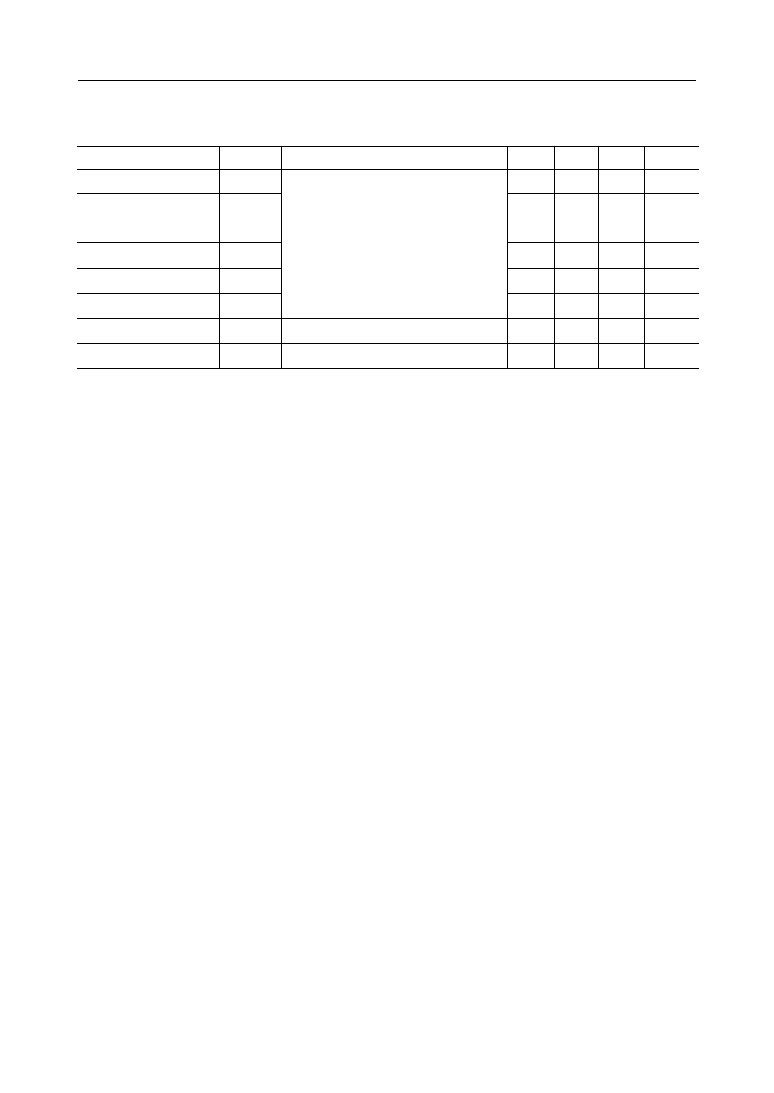
A/D Converter Characteristics
(V
DD
=4.5 to 5.5V/2.7 to 4.5V, GND=0V, Ta=-40 to +85∞C)
Parameter
Symbol
Condition
Min.
Max.
Unit
Resolution
n
--
bit
Absolute Error
E
L
+1.5/+2
Differential Linearity Error
E
D
±0.5/±1
Zero Point Error
E
ZS
+1.5/+2
Full Scale Error
E
FS
≠1.5/≠2
Crosstalk
E
CT
±0.5/±1
Analog input source impedance
R
I
£
5kW
Typ.
8
--
--
--
--
--
--
--
--
--
--
--
Conversion time *
t
CONV
--
16/32
--
≠1.5/≠2
See the recommended circuit (Fig. 3).
See the measuring circuit (Fig. 4).
f
OSC
=10 MHz / 5 MHz
LSB
LSB
LSB
LSB
LSB
m
s/CH
*
14.8/2.96ms/CH for the one time conversion follows setting the GO bit.
Definitions of Terms
(1)
Resolution
The minimum distinguishable analog value. For 8 bits, 2
8
=256, i.e. (V
RH
≠V
RL
)
˜
256.
(2)
Linearity Error
The variance between the ideal conversion characteristics as an 8-bit A/D converter and
actual conversion characteristics (does not include quantatized error).
The ideal conversion characteristics refer to steps of the voltage between V
RH
and V
RL
into 256 intervals.
(3)
Differential Linearity Error
Indicates the smoothness of the conversion. The width of analog input voltage
corresponding to the change by one bit of digital output is 1 LSB = (V
RH
-V
RL
)
˜
256
ideally. The variance between this ideal bit size and bit size at arbitrary point in the
conversion range.
(4)
Zero Scale Error
The variance between the ideal conversion characteristics at the switching point of digital
outputs "000H to 001H" and actual conversion characteristics.
(5)
Full Scale Error
The variance between the ideal conversion characteristics at the switching point of digital
outputs "0FEH to 0FFH" and actual conversion characteristics.
18/22
° Semiconductor
MSM65522/65P522
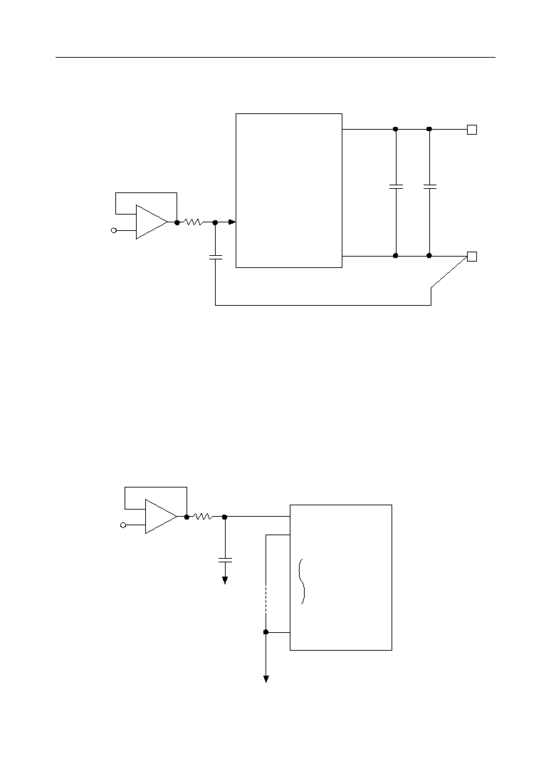
Figure 4. Crosstalk Measuring Circuit
≠
+
Analog Voltage
Input
0.1
m
F
5kW
AI0
AI1
AI7
V
REF
or AGND
Crosstalk is defined
as the difference of
A/D conversion result
between supplying
the same voltage to AI0
to AI7 and supplying
voltage shown in this
diagram.
Figure 3. Recommended Circuit
≠
+
R
1
Analog Voltage
Input
0.1
m
F
0.1
m
F
47
m
F
+
0V
AI0 to 7
V
DD
GND
MSM65522
R
I
(Analog input source impedance)£5kW
V
DD
19/22
° Semiconductor
MSM65522/65P522
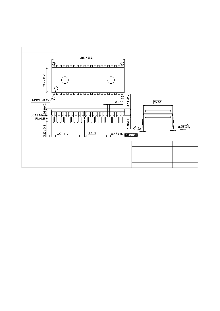
(Unit : mm)
PACKAGE DIMENSIONS
Notes for Mounting the Surface Mount Type Package
The SOP, QFP, TSOP, SOJ, QFJ (PLCC), SHP and BGA are surface mount type packages, which
are very susceptible to heat in reflow mounting and humidity absorbed in storage.
Therefore, before you perform reflow mounting, contact Oki's responsible sales person for the
product name, package name, pin number, package code and desired mounting conditions
(reflow method, temperature and times).
SDIP42-P-600-1.78
Package material
Lead frame material
Pin treatment
Solder plate thickness
Package weight (g)
Epoxy resin
42 alloy
Solder plating
5 mm or more
4.52 TYP.
20/22
° Semiconductor
MSM65522/65P522
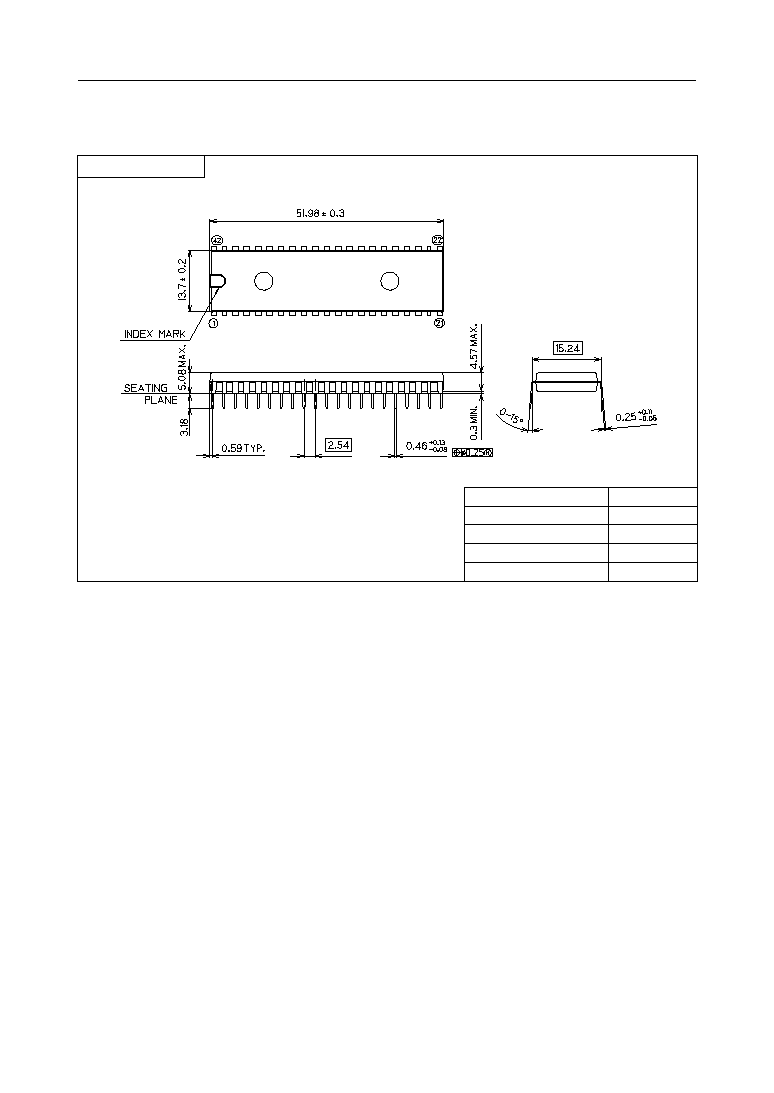
(Unit : mm)
Notes for Mounting the Surface Mount Type Package
The SOP, QFP, TSOP, SOJ, QFJ (PLCC), SHP and BGA are surface mount type packages, which
are very susceptible to heat in reflow mounting and humidity absorbed in storage.
Therefore, before you perform reflow mounting, contact Oki's responsible sales person for the
product name, package name, pin number, package code and desired mounting conditions
(reflow method, temperature and times).
DIP42-P-600-2.54
Package material
Lead frame material
Pin treatment
Solder plate thickness
Package weight (g)
Epoxy resin
42 alloy
Solder plating
5 mm or more
6.20 TYP.
21/22
° Semiconductor
MSM65522/65P522
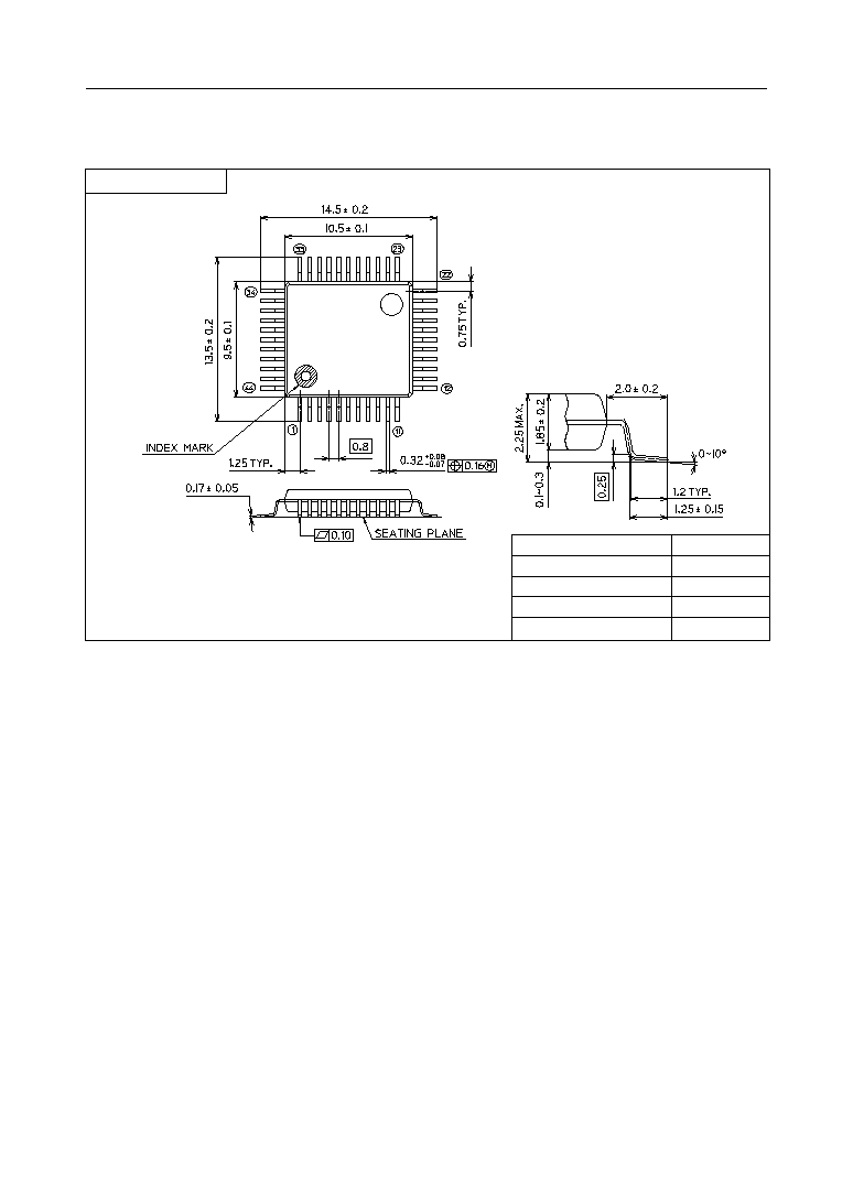
(Unit : mm)
Notes for Mounting the Surface Mount Type Package
The SOP, QFP, TSOP, SOJ, QFJ (PLCC), SHP and BGA are surface mount type packages, which
are very susceptible to heat in reflow mounting and humidity absorbed in storage.
Therefore, before you perform reflow mounting, contact Oki's responsible sales person for the
product name, package name, pin number, package code and desired mounting conditions
(reflow method, temperature and times).
Package material
Lead frame material
Pin treatment
Solder plate thickness
Package weight (g)
Epoxy resin
42 alloy
Solder plating
5 mm or more
0.41 TYP.
QFP44-P-910-0.80-2K
Mirror finish
22/22
° Semiconductor
MSM65522/65P522
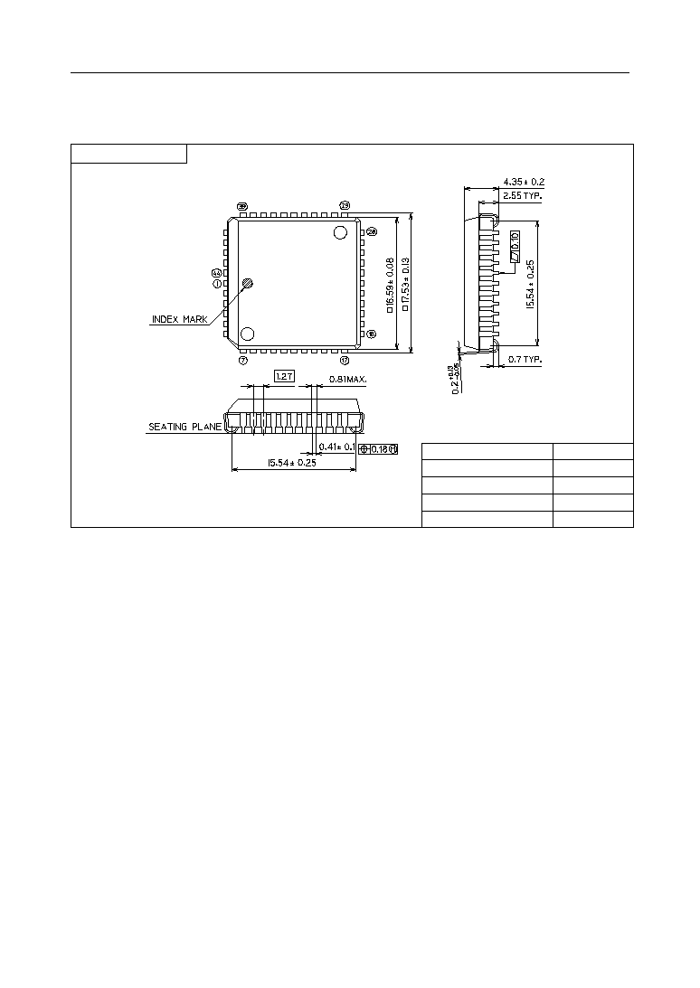
(Unit : mm)
Notes for Mounting the Surface Mount Type Package
The SOP, QFP, TSOP, SOJ, QFJ (PLCC), SHP and BGA are surface mount type packages, which
are very susceptible to heat in reflow mounting and humidity absorbed in storage.
Therefore, before you perform reflow mounting, contact Oki's responsible sales person for the
product name, package name, pin number, package code and desired mounting conditions
(reflow method, temperature and times).
QFJ44-P-S650-1.27
Package material
Lead frame material
Pin treatment
Solder plate thickness
Package weight (g)
Epoxy resin
Cu alloy
Solder plating
5 mm or more
2.00 TYP.
Mirror finish