 | –≠–ª–µ–∫—Ç—Ä–æ–Ω–Ω—ã–π –∫–æ–º–ø–æ–Ω–µ–Ω—Ç: MSM6653A | –°–∫–∞—á–∞—Ç—å:  PDF PDF  ZIP ZIP |

1/45
° Semiconductor
MSM6652/53/54/55/56-xxx, MSM6652A/53A/
54A/55A/56A/58A-xxx, MSM66P54-xx,
MSM66P56-xx, MSM6650
Internal Mask ROM Voice Synthesis IC, Internal One-Time-Programmable (OTP) ROM
Voice Synthesis IC, External ROM Drive Voice Synthesis IC
This document contains minimum specifications. For full specifications, please contact your
nearest Oki office or representative.
FEDL6650-03
GENERAL DESCRIPTION
The MSM6650 family is the successor to OKI's MSM6375 family. To ensure high-quality voice
synthesis, the MSM6650 family members offer adaptive differential pulse-code modulation (ADPCM)
playback, pulse-code modulation (PCM) playback, 12-bit D/A conversion, and on-chip ≠40 dB/
octave low-pass filter (LPF).
The conventional "beep" tones and 2-channel playback are now easier to use. OKI has added
additional functions such as melody play, fade-out, and random playback. OKI has improved
external control by adding an Edit ROM. The Edit ROM can be used to form sentences by linking
phrases.
The MSM6650 family members can support a variety of applications as it can function in either
Standalone Mode or Microcontroller Interface Mode. In Microcontroller Interface Mode, serial input
control is available. Serial input control minimizes the number of microcontroller port pins required
for voice synthesis control. The MSM6650 family includes an internal mask ROM version, internal
one-time-programmable (OTP) ROM version, and external ROM version. The features of the
MSM6650 family devices are as follows.
∑ MSM6652/53/54/55/56-xxx
These devices are single-chip voice synthesizers with an on-chip mask ROM using the CMOS
technology.
Standalone Mode or Microcontroller Interface Mode can be selected by mask option.
∑ MSM6652A/53A/54A/55A/56A/58A-xxx
The trial production period for these devices is shorter than those described above. These devices
are suitable for developing prototype models and concept demonstration of new products.
∑ MSM66P54-xx, MSM66P56-xx
The device is a single-chip CMOS voice synthesizer with one-time-programmable (OTP) ROM.
Standalone and Microcontroller Interface Modes are selected by using a code (01-04).
The user can easily write voice data using the development tool AR761 or AR762, or P54 adapter.
Unlike the mask ROM version, the OTP version is suited to applications which requires a small lot
production of different type devices or short delivery time.
∑ MSM6650
The MSM6650 device can directly connect external ROM or EPROM of up to 64 Mbits, which
stores voice data.
This device is ideally suited to an evaluation IC for the MSM6650 family because its circuit
configuration is identical to those of the mask ROM-based and OTP version devices.
This version: Jul. 2000
Previous version: Sep. 1999
2/45
° Semiconductor
MSM6650 Family
FEDL6650-03
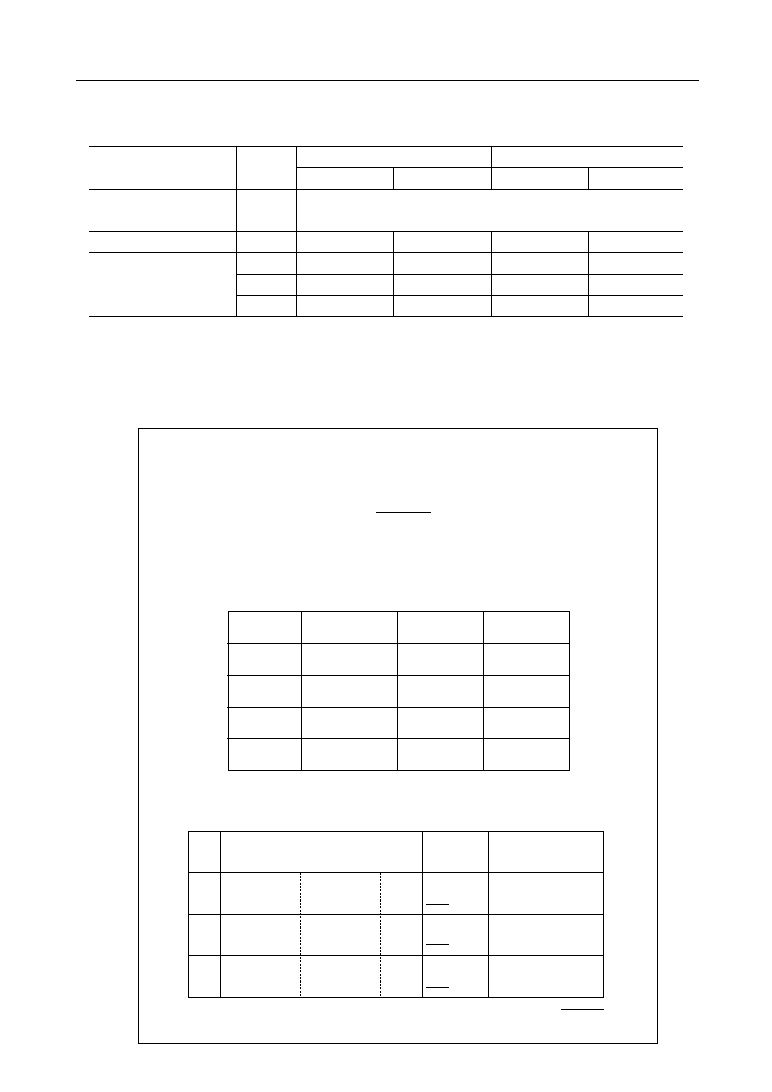
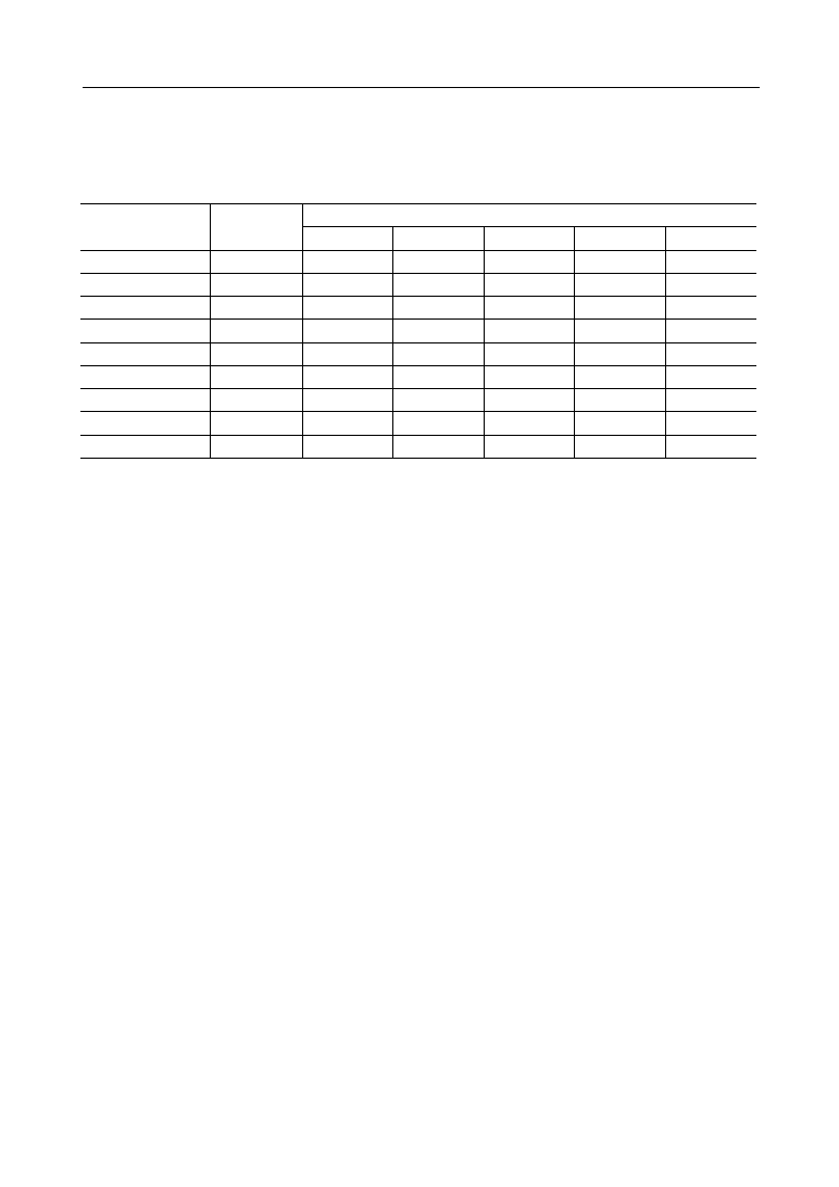
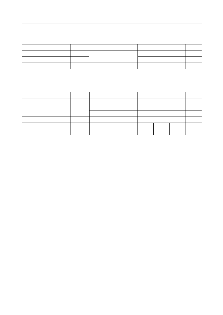
∑ Option Table
Option
Input
Interface mode
Standby
conversion
Option A
Option B
Option C
Option D
Microcontroller
Standalone
Microcontroller
Standalone
Serial
Parallel
--
--
--
--
Yes
No
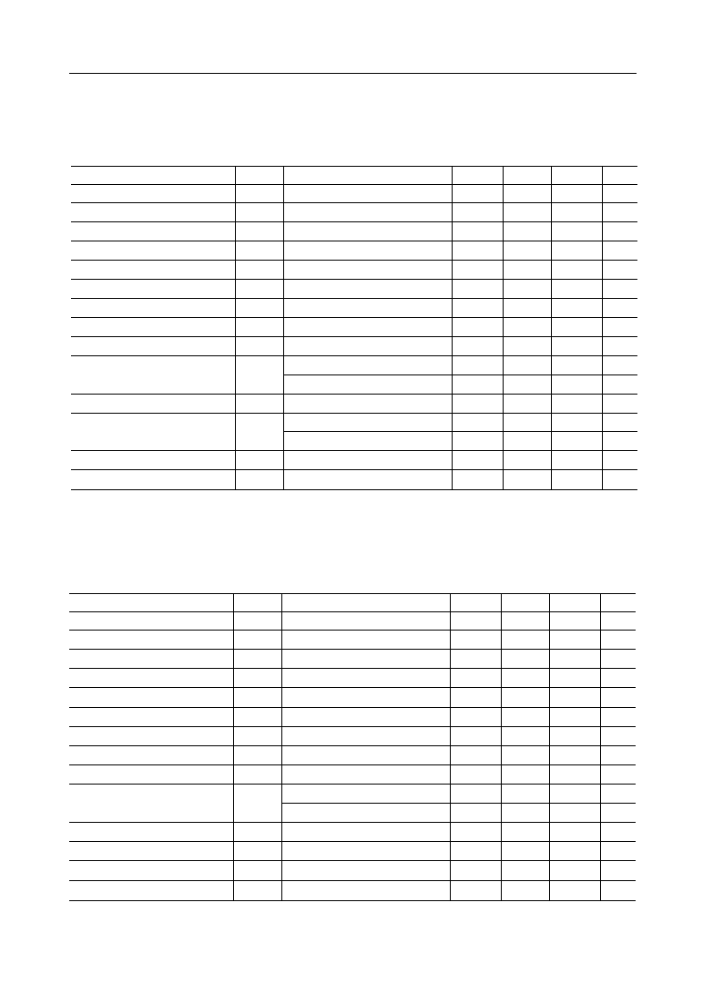
Item
Ceramic
sample
Mold
sample
Mass
produc-
tion
Package
(circle the desired one)
Quantity
Note
18-pin DIP
(ceramic)
18-pin DIP
(plastic)
18-pin DIP
(plastic)
24-pin SOP
(ceramic)
24-pin SOP
(plastic)
24-pin SOP
(plastic)
chip
chip
chip
pcs
pcs
pcs per lot
monthly
Up to 10 samples.
Operating temp. :
10 to 30∞C
Up to 50 samples
Option List
Oki Electric Industry Co., Ltd.
Date:
You are requested to develop MSM665X-XXX on the following conditions.
1. Options
There are four options for the MSM6650 family.
Choose and circle the desired option.
2. Package and quantity
Signed by
Title :
Company name :
*1. The options for the mask ROM-based devices are mask options. The user should send OKI an
option list before starting development. A sample of option list is shown below.
*2. A code of OTP version device corresponds to one of the options. The user should specify either
MSM66P54-03 or MSM66P54-04 or MSM66P56-03 or MSM66P56-04. (In this case, no option list
is required.)
Pin Name
Microcontroller Interface Mode
Serial Input
Parallel Input
With Standby
No Standby
STBY
--
--
"L"
"H"
MSM6650
SERIAL
"H"
"L"
"L"
"L"
CPU
"H"
"H"
"L"
"L"
MSM66P54/P56
--
≠01
≠02
≠03
≠04
MSM6652/53/54/55/56
--
Standalone Mode
Mask Option
*2
MSM6652A/53A/54A/55A/56A/58A
*1

3/45
° Semiconductor
MSM6650 Family
FEDL6650-03
STANDALONE MODE
FEATURES
Note: Actual voice ROM area is smaller by 22 Kbits.
∑ 4-bit ADPCM or 8-bit PCM sound generation
∑ Melody function
∑ Edit ROM function
∑ Two-channel mixing function
∑ Built-in random playback function
∑ Fade-out function via four-step sound volume attenuation
∑ Built-in beep tone of 0.5 kHz, 1.0 kHz, 1.3 kHz, or 2.0 kHz selectable with a specific code
∑ Sampling frequency of 4.0 kHz, 5.3 kHz, 6.4 kHz, 8.0 kHz, 10.6 kHz, 12.8 kHz, 16.0 kHz, or 32.0 kHz
(32 kHz sampling is not possible when using RC oscillation)
∑ Up to 120 phrases
∑ Built-in 12-bit D/A converter
∑ Built-in ≠40 dB/octave low-pass filter
∑ Standby function
∑ Selectable RC or ceramic oscillation
∑ Package options:
18-pin plastic DIP (DIP18-P-300-2.54)
(Product name: MSM6652-xxxRS/MSM6653-xxxRS/
MSM6654-xxxRS/MSM6655-xxxRS/
MSM6656-xxxRS/MSM6652A-xxxRS/
MSM6653A-xxxRS/MSM6654A-xxxRS/
MSM6655A-xxxRS/MSM6656A-xxxRS/
MSM6658A-xxxRS)
24-pin plastic SOP (SOP24-P-430-1.27-K) (Product name: MSM6652-xxxGS-K/MSM6653-xxxGS-K/
MSM6654-xxxGS-K/MSM6655-xxxGS-K/
MSM6656-xxxGS-K/MSM6652A-xxxGS-K/
MSM6653A-xxxGS-K/MSM6654A-xxxGS-K/
MSM6655A-xxxGS-K/MSM6656A-xxxGS-K/
MSM6658A-xxxGS-K/MSM66P54-03GS-K/
MSM66P54-04GS-K/MSM66P56-03GS-K/
MSM66P56-04GS-K)
20-pin plastic DIP (DIP20-P-300-2.54-W1) (Product name:
MSM66P54-03RS/MSM66P54-04RS/
MSM66P56-03RS/MSM66P56-04RS)
64-pin plastic QFP (QFP64-P-1420-1.00-BK) (Product name:
MSM6650GS-BK)
64-pin plastic SDIP (SDIP64-P-750-1.778)
(Product name:
MSM6650SS)
Device name
ROM size
Maximum playback time (sec)
f
SAM
=4.0 kHz
f
SAM
=6.4 kHz
f
SAM
=8.0 kHz
f
SAM
=16 kHz
MSM6650
64 Mbits (Max)
4194.3
2620.5
2096.4
1048.2
MSM6656, 6656A
2 Mbits
129.1
80.7
64.5
32.2
MSM6655, 6655A
1.5 Mbits
96.5
60.3
48.2
24.1
MSM6654, 6654A
1 Mbit
63.8
39.9
31.9
15.9
MSM6653, 6653A
544 Kbits
31.2
19.5
15.6
7.8
MSM6652, 6652A
288 Kbits
16.9
10.5
8.4
4.2
MSM66P54
1 Mbit
63.8
39.9
31.9
15.9
129.1
80.7
64.5
32.2
MSM6658A
4 Mbits
259.7
162.9
129.8
64.9
MSM66P56
2 Mbit
129.1
80.7
64.5
32.2
4/45
° Semiconductor
MSM6650 Family
FEDL6650-03
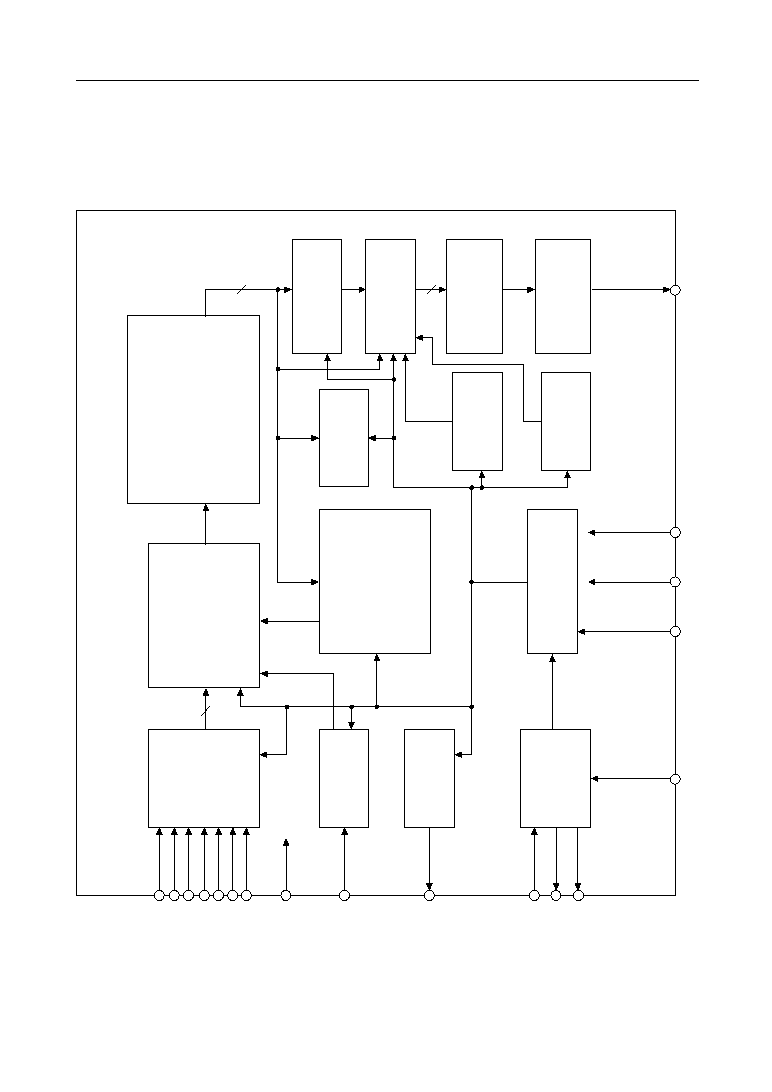
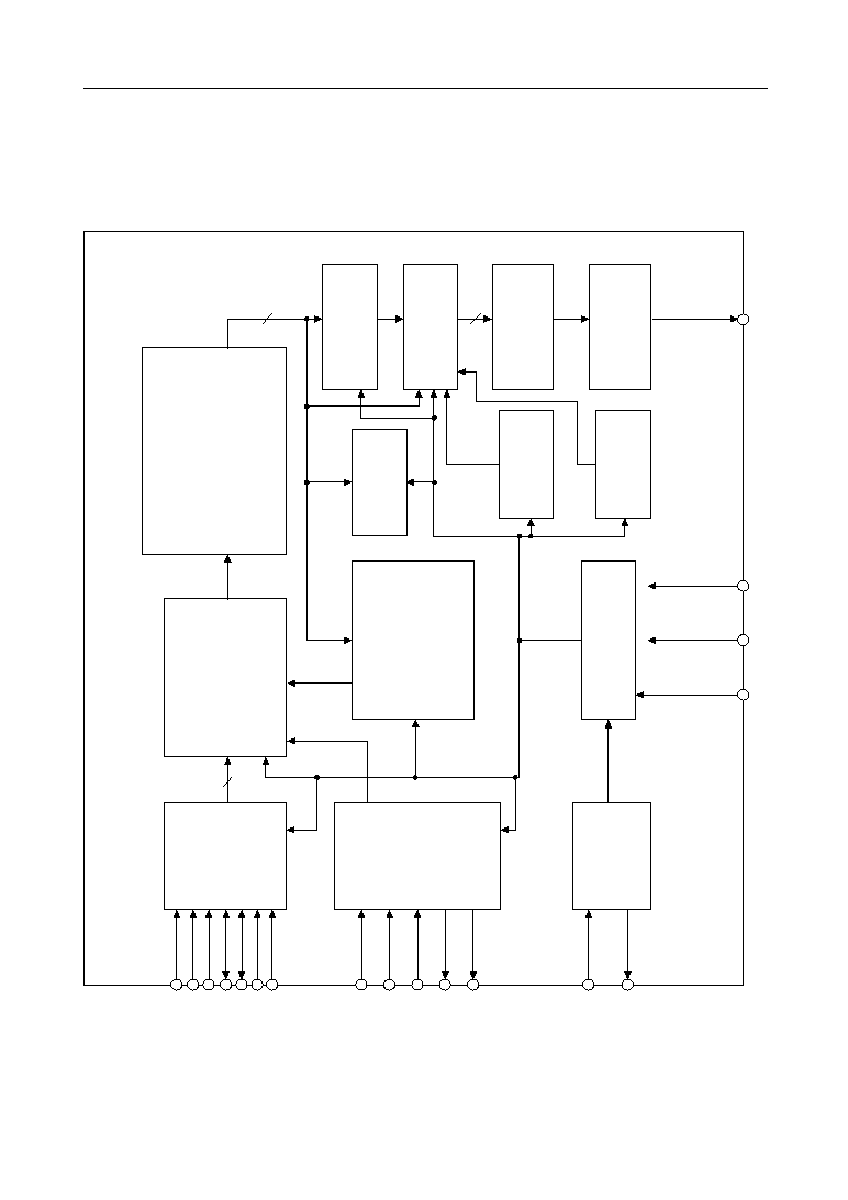
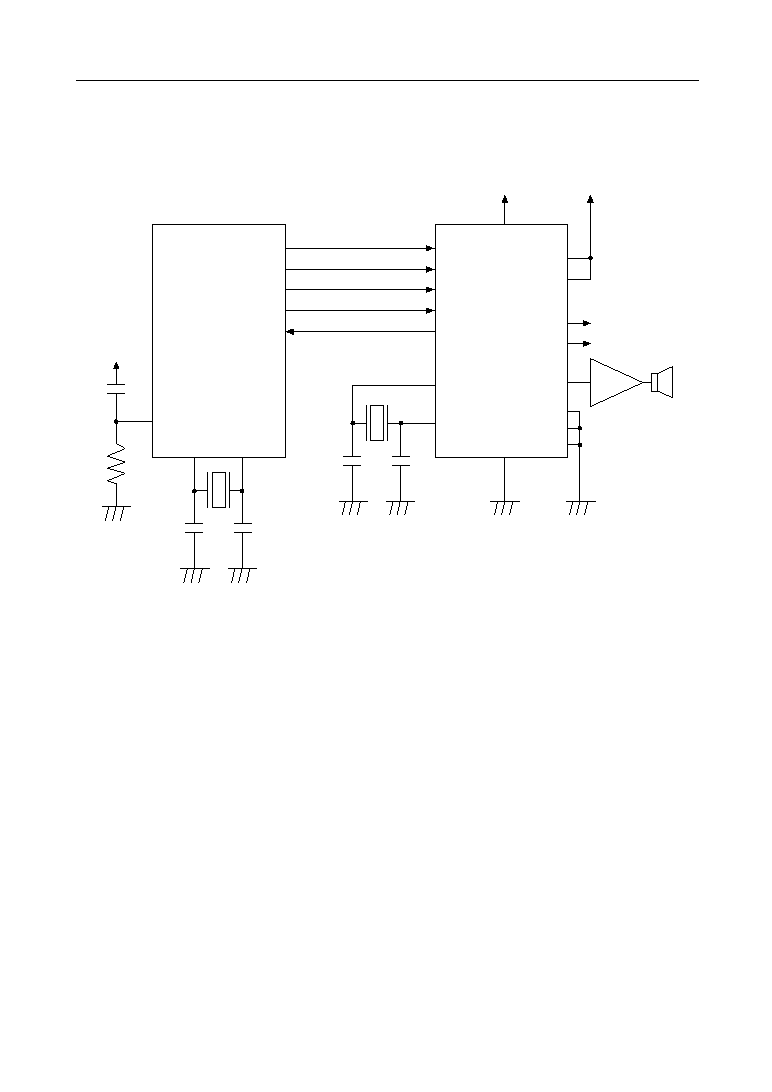
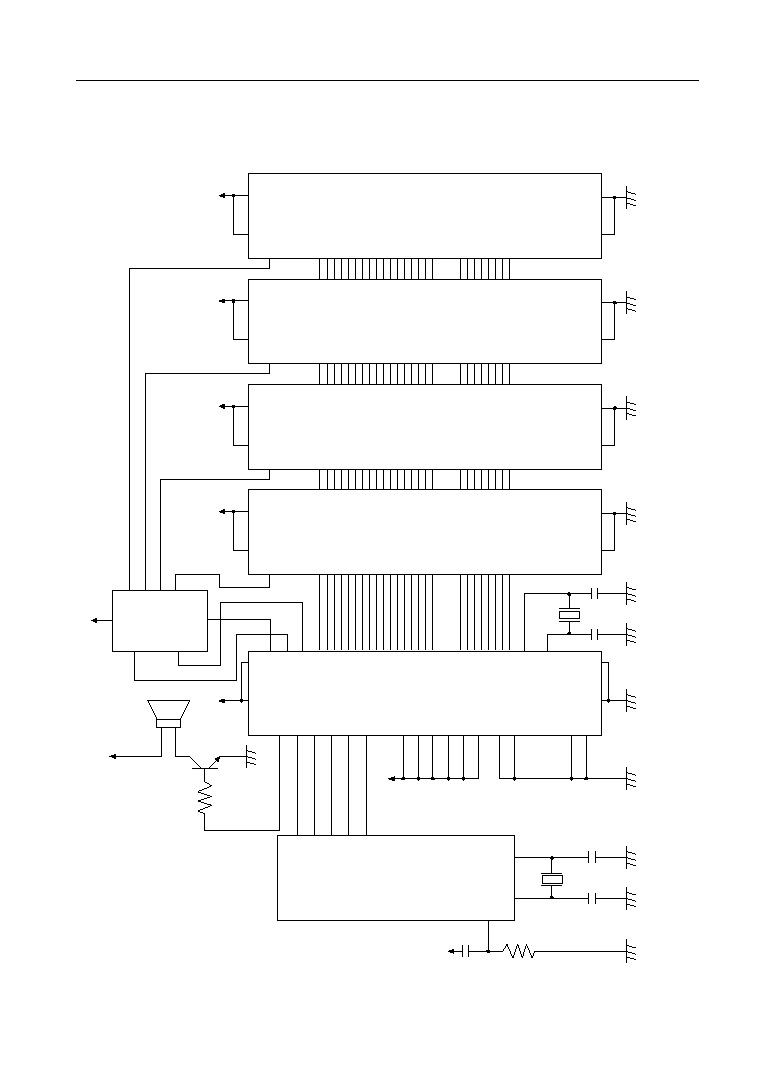
BLOCK DIAGRAMS
MSM6652/53/54/55/56-xxx
MSM6652A/53A/54A/55A/56A/58A-xxx
ROM
(Containing 22-Kbit Phrase Control
Table & Phrase Address Table)
16-
Bit
(MSM6652/52A)
17-
Bit
(MSM6653/53A)
17-
Bit
(MSM6654/54A)
18-
Bit
(MSM6655/55A)
18-
Bit
(MSM6656/56A)
19-
Bit
(MSM6658A)
Multiplexer
Address &
Switching
Controller
7
ADPCM
Synthesizer
PCM
Synthesizer
12
8
12-Bit
DAC
LPF
AOUT
DATA
Controller
Melody
Generator
BEEP Tone
Generator
16-
Bit
(MSM6652/52A)
17-
Bit
(MSM6653/53A)
17-
Bit
(MSM6654/54A)
18-
Bit
(MSM6655/55A)
18-
Bit
(MSM6656/56A)
19-
Bit
(MSM6658A)
Address Counter
Timing Controller
GND
V
DD
RESET
Random
Circuit
I/O
Interface
OSC
Ceramic/
Crystal/RC
XT/
CR
A2
A1
A0
SW3
SW2
SW1
SW0
TEST
RND
BUSY
OSC1
OSC2
OSC3
(MSM6652/52A)
(MSM6653/53A)
(MSM6654/54A)
(MSM6655/55A)
(MSM6656/56A)
(MSM6658A)
288-Kbit
544-Kbit
1-Mbit
1.5-Mbit
2-Mbit
4-Mbit
5/45
° Semiconductor
MSM6650 Family
FEDL6650-03
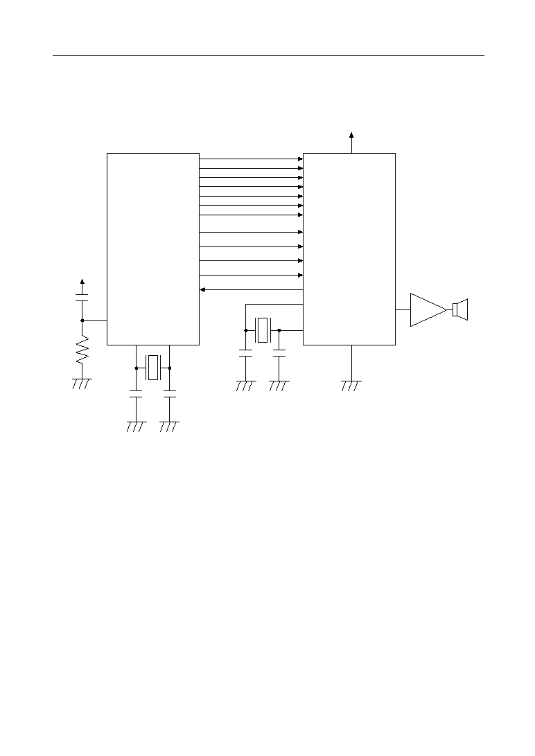
MSM66P54/P56-xx
A2
A1
A0
SW3
SW2
SW1
SW0
TEST
RND
BUSY
OSC1
OSC2
OSC3
XT/
CR
RESET
V
DD
GND
AOUT
PGM
V
PP
Address &
Switching
Controller
Random
Circuit
I/O
Interface
OSC
(Ceramic/
Crystal/RC)
17-Bit (MSM66P54-xx)
18-Bit (MSM66P56-xx)
Multiplexer
17-Bit (MSM66P54-xx)
18-Bit (MSM66P56-xx)
Address Counter
Timing Controller
Program Circuit
1-Mbit OTP ROM (MSM66P54-xx)
2-Mbit OTP ROM (MSM66P56-xx)
(Containing 22-Kbit Phrase Control
Table & Phrase Address Table)
DATA
Controller
ADPCM
Synthesizer
PCM
Synthesizer
Melody
Generator
BEEP Tone
Generator
12-
Bit
DAC
LPF
12
8
7

6/45
° Semiconductor
MSM6650 Family
FEDL6650-03
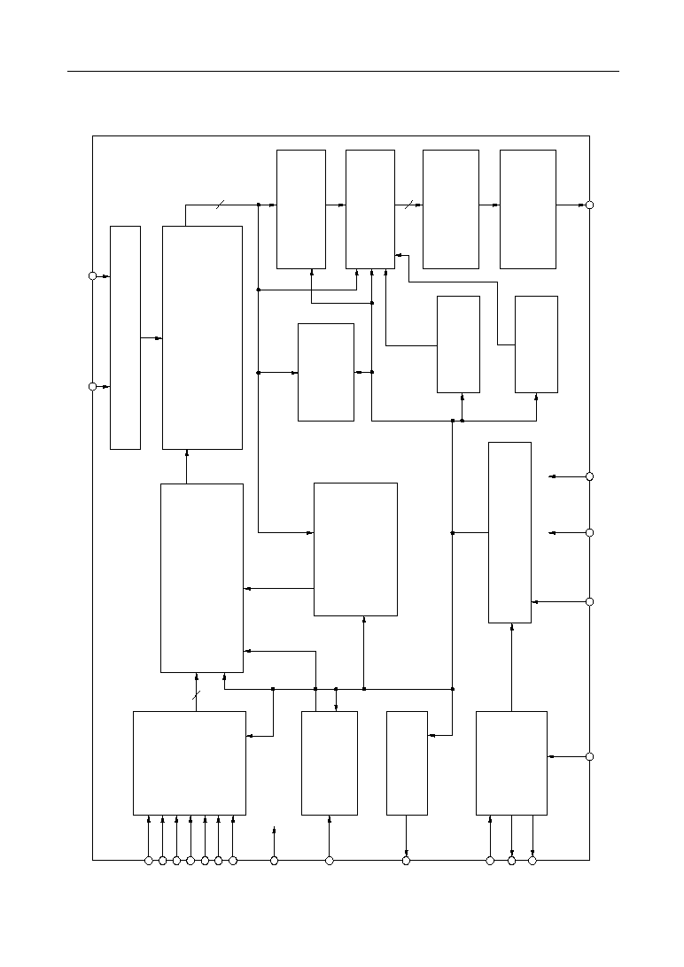
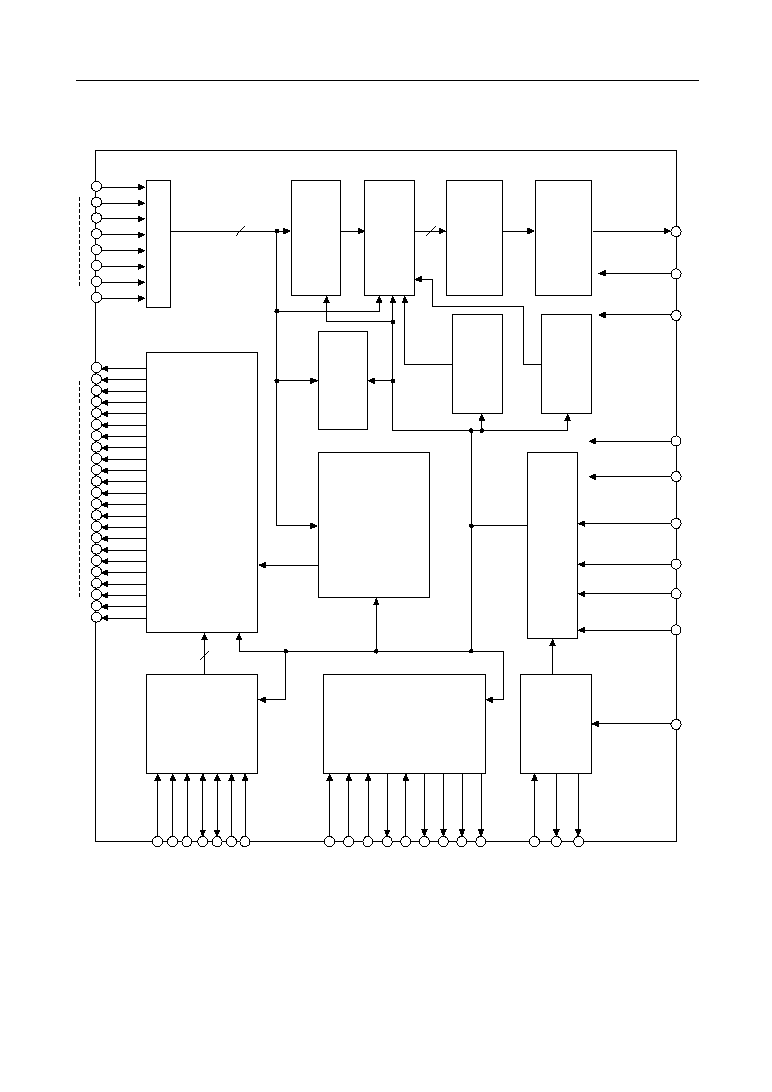
MSM6650
8-Bit LATCH
23-Bit Multiplexer
Address &
Switching
Controller
7
ADPCM
Synthesizer
PCM
Synthesizer
12
8
12-Bit
DAC
LPF
AOUT
DATA
Controller
Melody
Generator
BEEP Tone
Generator
23-Bit Address
Counter
Timing Controller
DGND
DV
DD
RESET
Random
Circuit
I/O
Interface
OSC
(Ceramic/
Crystal/RC)
XT/
CR
A2
A1
A0
SW3
SW2
SW1
SW0
TEST1, 3
RND
CE
RCS
BUSY
NAR
IBUSY
STANDBY
XT/OSC1
XT/OSC2
OSC3
AV
DD
AGND
TEST2
CPU
STBY
RA22
RA0
D7
D0
7/45
° Semiconductor
MSM6650 Family
FEDL6650-03
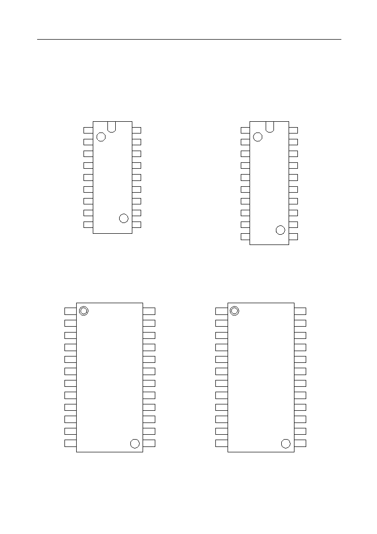
18-Pin Plastic DIP
1
2
3
4
5
6
7
8
9
18
17
16
15
14
13
12
11
10
TEST
A2
A1
A0
RESET
XT/
CR
AOUT
SW3
SW2
SW1
SW0
RND
OSC3
OSC2
OSC1
MSM6652-6658A (Mask ROM)
24-Pin Plastic SOP
1
2
3
4
5
6
7
8
9
10
11
12
24
23
22
21
20
19
18
17
16
15
14
13
V
DD
OSC1
OSC2
NC
OSC3
NC
NC
RND
SW0
SW1
SW2
SW3
GND
AOUT
XT/
CR
NC
BUSY
NC
NC
RESET
TEST
A2
A1
A0
BUSY
GND
V
DD
MSM6652-6658A (Mask ROM)
20-Pin Plastic DIP
1
2
3
4
5
6
7
8
9
10
20
19
18
17
16
15
14
13
12
11
TEST
A2
A1
A0
V
PP
RESET
BUSY
XT/
CR
AOUT
GND
PGM
SW3
SW2
SW1
SW0
RND
OSC3
OSC2
OSC1
V
DD
MSM66P54/P56 (OTP)
24-Pin Plastic SOP
1
2
3
4
5
6
7
8
9
10
11
12
24
23
22
21
20
19
18
17
16
15
14
13
V
DD
OSC1
OSC2
NC
OSC3
NC
PGM
RND
SW0
SW1
SW2
SW3
GND
AOUT
XT/
CR
NC
BUSY
NC
V
PP
RESET
TEST
A2
A1
A0
MSM66P54/P56 (OTP)
MSM6652-xxxRS, MSM6653-xxxRS, MSM6654-xxxRS,
MSM66P54-03/-04RS
MSM6655-xxxRS, MSM6656-xxxRS, MSM6652A-xxxRS,
MSM66P56-03/-04RS
MSM6653A-xxxRS, MSM6654A-xxxRS, MSM6655A-xxxRS,
MSM6656A-xxxRS, MSM6658A-xxxRS
PIN CONFIGURATION (TOP VIEW)
The MSM66P54-xx and MSM66P56-xx has two more pins than the MSM6652-6658A while their pin
configurations are identical.
The additional two pins (V
PP
, PGM) of the MSM66P54-xx/P56-xx may be open at playback after
completion of writing.
MSM6652-xxxGS-K, MSM6653-xxxGS-K,
MSM66P54-03/-04GS-K
MSM6654-xxxGS-K, MSM6655-xxxGS-K,
MSM66P56-03/-04GS-K
MSM6656-xxxGS-K, MSM6652A-xxxGS-K,
MSM6653A-xxxGS-K, MSM6654A-xxxGS-K,
MSM6655A-xxxGS-K, MSM6656A-xxxGS-K,
MSM6658A-xxxGS-K
8/45
° Semiconductor
MSM6650 Family
FEDL6650-03
MSM6650
Product name: MSM6650GS-BK
,
1
NC
BUSY
NAR
NC
AOUT
AGND
DGND
AV
DD
DV
DD
XT/OSC1
XT/OSC2
OSC3
TEST1
RND
XT/
CR
CPU
TEST2
IBUSY
NC
RA10
RA9
RA8
RA7
RA6
RA5
RA4
RA3
RA2
RA1
RA0
D7
D6
D5
D4
D3
D2
D1
NC
STBY
RA22
RA21
RA20
RA19
RA18
RA17
RA16
RA15
RA14
RA13
RA12
RA11
STANDBY
SW0
SW1
SW2
SW3
A0
A1
A2
TEST3
RESET
CE
RCS
D0
2
3
4
5
6
7
8
9
10
11
12
13
14
15
16
17
18
19
20
21
22
23
24
25
26
27
28
29
30
31
32
33
34
35
36
37
38
39
40
41
42
43
44
45
46
47
48
49
50
51
52
53
54
55
56
57
58
59
60
61
62
63
64
NC : No connection
64-Pin Plastic QFP
9/45
° Semiconductor
MSM6650 Family
FEDL6650-03
NC : No connection
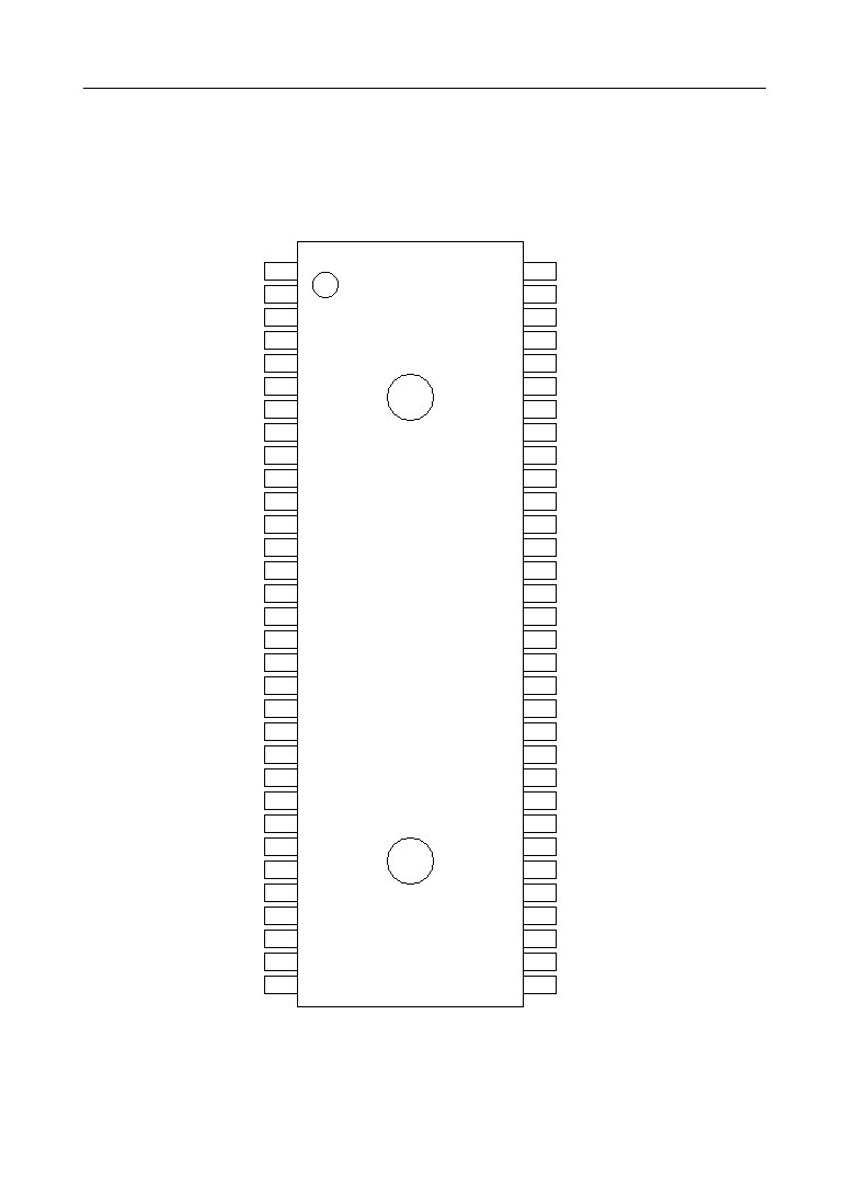
64-Pin Plastic SDIP
20
1
2
3
4
5
6
7
8
9
10
11
12
13
14
15
16
17
18
19
CE
XT/OSC2
OSC3
TEST1
RND
XT/
CR
CPU
TEST2
IBUSY
NC
STANDBY
SW0
SW1
SW2
SW3
A0
A1
A2
TEST3
RESET
RA13
XT/OSC1
DV
DD
AV
DD
DGND
AGND
AOUT
NAR
BUSY
NC
STBY
RA22
RA21
RA20
RA19
RA18
RA17
RA16
RA15
RA14
45
64
63
62
61
60
59
58
57
56
55
54
53
52
51
50
49
48
47
46
21
22
23
24
25
26
27
28
29
30
31
32
44
43
42
41
40
39
38
37
36
35
34
33
RCS
RA12
D0
RA11
NC
RA10
D1
NC
D2
RA9
D3
RA8
D4
RA7
D5
RA6
D6
RA5
D7
RA4
RA0
RA3
RA1
RA2
Product name: MSM6650SS
10/45
° Semiconductor
MSM6650 Family
FEDL6650-03
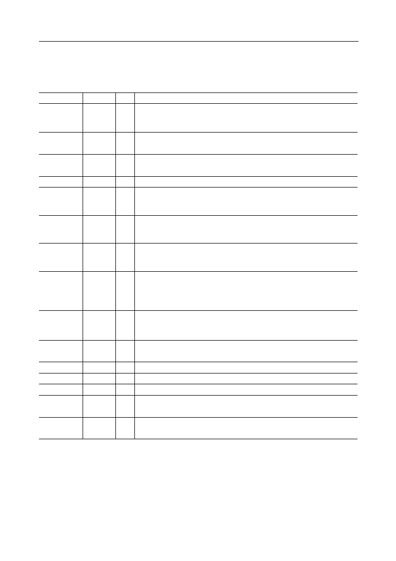
PIN DESCRIPTIONS
1. MSM6652/53/54/55/56-xxx, MSM6652A/53A/54A/55A/56A/58A-xxx
18-Pin plastic DIP
Symbol Type
Description
RESET
OSC2
OSC3
Reset. Setting this pin to "L" puts the LSI in standby status. At this time,
oscillation stops, AOUT is pulled to GND, and the deveice is initialized.
This pin has an internal pull-up resistor.
I
O
O
RND
SW0-SW3
A0-A2
I
I
I
BUSY
O
XT/
CR
I
Busy. This pin outputs a "L" level during playback. At power-on, this pin is at "H"
level.
XT/
CR selectable pin. Set to "H" level when using ceramic oscillation. Set to
"L" level when using RC oscillation.
AOUT
O
Sound Output. This is the synthesized output pin of the internal low-pass filter.
Oscillator 1. This pin is a ceramic oscillator connection pin when using ceramic
oscillation. This pin is an RC connection pin when using RC oscillation.
When using an external clock, use this pin as the clock input.
OSC1
I
Oscillator 2. This pin is a ceramic oscillator connection pin when using a
ceramic oscillator. This is an RC connection pin when using RC oscillation.
Leave open if using an external clock. OSC2 outputs a "L" level in standby status.
Oscillator 3. Leave open if using a ceramic oscillator. This pin is the RC
connection pin when using RC oscillation. When RC oscillation is selected, OSC3
outputs a "H" level in standby status.
Random Playback. Random playback starts when the
RND pin is set to a "L"
level. At the fall of
RND, addresses from the random address playback circuit
inside the IC are fetched. Set to a "H" level if random playback is not used.
This pin has an internal pull-up resistor.
Phrase Inputs. These pins are phrase input pins corresponding to playback.
If the input changes, SW0 to SW3 pins capture address data after 16 ms and
speech playback commences. These pins have internal pull-down resistors.
Phrase Inputs. Phrase input pins correspoding to playback. The A0 input
becomes invalid when the random playback function is used.
TEST
I
Test Mode. Set to "H" level. This pin has an internal pull-up resistor.
Pin
5
12
13
14
15-18
1-3
6
7
8
11
4
GND
--
Ground.
V
DD
--
Power supply. Insert a 0.1
mF or more bypass capacitor between this pin and GND.
9
10
11/45
° Semiconductor
MSM6650 Family
FEDL6650-03
Symbol Type
Description
RESET
Reset. Setting this pin to "L" puts the LSI in standby status. At this time,
oscillation stops, AOUT is pulled to GND, and the deveice is initialized.
This pin has an internal pull-up resistor.
I
BUSY
O
XT/
CR
I
Busy. This pin outputs a "L" level during playback. At power-on, this pin is at "H"
level.
XT/
CR selectable pin. Set to "H" level when using ceramic oscillation. Set to
"L" level when using RC oscillation.
AOUT
O
Sound Output. This is the synthesized output pin of the internal low-pass filter.
Pin
6
7
8
9
OSC2
OSC3
O
O
RND
SW0-SW3
A0-A2
I
I
I
Oscillator 1. This pin is a ceramic oscillator connection pin when using ceramic
oscillation. This pin is an RC connection pin when using RC oscillation.
When using an external clock, use this pin as the clock input.
OSC1
I
Oscillator 2. This pin is a ceramic oscillator connection pin when using a
ceramic oscillator. This is an RC connection pin when using RC oscillation.
Leave open if using an external clock. OSC2 outputs a "L" level in standby status.
Oscillator 3. Leave open if using a ceramic oscillator. This pin is the RC
connection pin when using RC oscillation. When RC oscillation is selected, OSC3
outputs a "H" level in standby status.
Random Playback. Random playback starts when the
RND pin is set to a "L"
level. At the fall of
RND, addresses from the random address playback circuit
inside the IC are fetched. Set to a "H" level if random playback is not used.
This pin has an internal pull-up resistor.
Phrase Inputs. These pins are phrase input pins corresponding to playback.
If the input changes, SW0 to SW3 pins capture address data after 16 ms and
speech playback commences. These pins have internal pull-down resistors.
Phrase Inputs. Phrase input pins correspoding to playback. The A0 input
becomes invalid when the random playback function is used.
GND
--
Ground.
V
DD
--
Power supply. Insert a 0.1
mF or more bypass capacitor between this pin and GND.
TEST
I
Test Mode. Set to "H" level. This pin has an internal pull-up resistor.
13
14
15
16-19
2-4
12
10
11
5
V
PP
--
PGM
I
Power supply used when writing data to internal OTP ROM. Leave open or set to
"H" level during playback.
Interface with voice analysis edit tool AR203 or AR204. Set to "L" level or leave
open during playback.
1
20
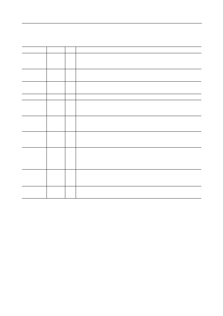
2.MSM66P54-xx, MSM66P56-xx
20-Pin plastic DIP
12/45
° Semiconductor
MSM6650 Family
FEDL6650-03
3.MSM6652/53/54/55/56-xxx, MSM6652A/53A/54A/55A/56A/58A-xxx, MSM66P54-xx,
MSM66P56-xx
24-Pin plastic SOP
Symbol Type
Description
RESET
OSC2
OSC3
Reset. Setting this pin to "L" puts the LSI in standby status. At this time,
oscillation stops, AOUT is pulled to GND, and the deveice is initialized.
This pin has an internal pull-up resistor.
I
O
O
RND
SW0-SW3
A0-A2
I
I
I
BUSY
O
XT/
CR
I
Busy. This pin outputs a "L" level during playback. At power-on, this pin is at "H"
level.
XT/
CR selectable pin. Set to "H" level when using ceramic oscillation. Set to
"L" level when using RC oscillation.
AOUT
O
Sound Output. This is the synthesized output pin of the internal low-pass filter.
Oscillator 1. This pin is a ceramic oscillator connection pin when using ceramic
oscillation. This pin is an RC connection pin when using RC oscillation.
When using an external clock, use this pin as the clock input.
OSC1
I
Oscillator 2. This pin is a ceramic oscillator connection pin when using a
ceramic oscillator. This is an RC connection pin when using RC oscillation.
Leave open if using an external clock. OSC2 outputs a "L" level in standby status.
Oscillator 3. Leave open if using a ceramic oscillator. This pin is the RC
connection pin when using RC oscillation. When RC oscillation is selected, OSC3
outputs a "H" level in standby status.
Random Playback. Random playback starts when the
RND pin is set to a "L"
level. At the fall of
RND, addresses from the random address playback circuit
inside the IC are fetched. Set to a "H" level if random playback is not used.
This pin has an internal pull-up resistor.
Phrase Inputs. These pins are phrase input pins corresponding to playback.
If the input changes, SW0 to SW3 pins capture address data after 16 ms and
speech playback commences. These pins have internal pull-down resistors.
Phrase Inputs. Phrase input pins correspoding to playback. The A0 input
becomes invalid when the random playback function is used.
GND
--
Ground.
V
DD
--
Power supply. Insert a 0.1
mF or more bypass capacitor between this pin and GND.
TEST
I
Test Mode. Set to "H" level. This pin has an internal pull-up resistor.
Pin
17
3
5
8
9-12
13-15
20
22
23
2
24
1
16
V
PP
*
--
PGM*
I
Power supply used when writing data to internal OTP ROM. Leave open or set to
"H" level during playback.
Interface with voice analysis edit tool AR203 or AR204. Set to "L" level or leave
open during playback.
18
7
* Pins for MSM66P54/56-xx only
13/45
° Semiconductor
MSM6650 Family
FEDL6650-03
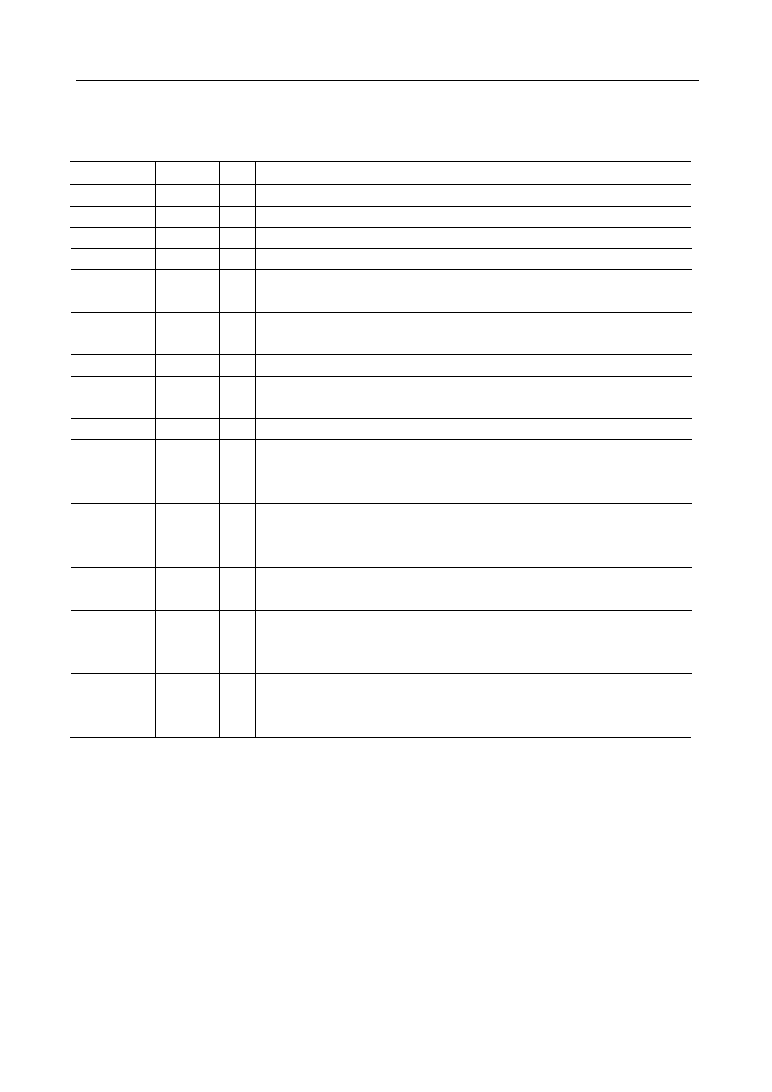
4.MSM6650
64-Pin plastic QFP (64-Pin plastic SDIP)
Symbol Type
Description
RESET
XT/OSC2
OSC3
Reset. Setting this pin to "L" puts the LSI in standby status. At this time,
oscillation stops, AOUT is pulled to GND, and the deveice is initialized.
This pin has an internal pull-up resistor.
I
O
O
RND
SW0-SW3
A0-A2
I
I
I
BUSY
O
XT/
CR
I
Busy. This pin outputs a "L" level during playback. At power-on, this pin is at "H"
level.
XT/
CR selectable pin. Set to "H" level when using ceramic oscillation. Set to
"L" level when using RC oscillation.
AOUT
O
Sound Output. This is the synthesized output pin of the internal low-pass filter.
Oscillator 1. This pin is a ceramic oscillator connection pin when using ceramic
oscillation. This pin is an RC connection pin when using RC oscillation.
When using an external clock, use this pin as the clock input.
XT/OSC1
I
Oscillator 2. This pin is a ceramic oscillator connection pin when using a
ceramic oscillator. This is an RC connection pin when using RC oscillation.
Leave open if using an external clock. OSC2 outputs a "L" level in standby status.
Oscillator 3. Leave open if using a ceramic oscillator. This pin is the RC
connection pin when using RC oscillation. When RC oscillation is selected, OSC3
outputs a "H" level in standby status.
Random Playback. Random playback starts when the
RND pin is set to a "L"
level. At the fall of
RND, addresses from the random address playback circuit
inside the IC are fetched. Set to a "H" level if random playback is not used.
This pin has an internal pull-up resistor.
Phrase Inputs. These pins are phrase input pins corresponding to playback.
If the input changes, SW0 to SW3 pins capture address data after 16 ms and
speech playback commences. These pins have internal pull-down resistors.
Phrase Inputs. Phrase input pins correspoding to playback. The A0 input
becomes invalid when the random playback function is used.
Pin
29(19)
11(1)
12(2)
14(4)
21-24
(11-14)
25-27
(15-17)
3(57)
15(5)
5 (59)
10(64)
14/45
° Semiconductor
MSM6650 Family
FEDL6650-03
CE
O
Chip Enable.
CE is a timing output pin to control read of external memory.
This pin outputs when
RCS is at the "L" level. This pin goes high impedance
when
RCS is at the "H" level.
CPU
I
CPU Mode. Set to "L" level to select Standalone Mode. Set to "H" level to select
Microcontroller Interface Mode.
D0-D7
I
External Memory Data Bus. Data is input when
RCS is low. When RCS is
high, these pins become low due to internal pull-down resistors.
IBUSY
O
I Busy. Outputs a "L" level during voice playback (except during standby
conversion time), or when the AOUT pin is at half V
DD
level.
RA0-RA22
O
External Memory Address. These are address pins for an external memory
output when
RCS is low. These pins become high impedance status if RCS is in
"H" level.
RCS
I
Read Chip Select. The data bits D0-D7 are internally pulled down when
RCS
is high. Addresses and
CE are output when RCS is at "L" level. The RA22-RA0
address pins and
CE pin become high impedance.
STBY
I
Standby Contorl. If set to "L" level, the MSM6650 enters standby mode 0.2
seconds after voice ends. If set to "H" level, the MSM6650 AOUT output maintains
half V
DD
after voice ends.
STANDBY
O
Standby Indicator. This output pin remains at "L" level during oscillation.
TEST1, 3
I
Test. Set these pins to "H" level. The
TEST1 and TEST3 pins have internal pull-up
resistor.
TEST2
I
Test. Set this pin to "L" level.
30 (20)
16 (6)
32, 34-40
(22, 24-30)
18 (8)
41-63
(31-40, 42-54)
31 (21)
64 (55)
20 (10)
13, 28 (3, 18)
17 (7)
Symbol Type
Description
AGND
--
Analog ground pin.
DGND
--
Digital ground pin.
AV
DD
--
Analog power pin. Insert a 0.1 mF or more bypass capacitor in between this pin and AGND.
DV
DD
--
Digiral power pin. Insert a 0.1 mF or more bypass capacitor in between this pin and DGND.
Pin
6 (60)
7 (61)
8 (62)
9 (63)
15/45
° Semiconductor
MSM6650 Family
FEDL6650-03
ABSOLUTE MAXIMUM RATINGS
Parameter
Symbol
Condition
Rating
Unit
Ta = 25∞C
--
(GND=0 V)
V
DD
≠0.3 to +7.0
V
Power supply voltage
V
IN
≠0.3 to V
DD
+0.3
V
Input voltage
T
STG
≠55 to +150
∞C
Storage temperature
RECOMMENDED OPERATING CONDITIONS
*
If RC oscillation is selected, 32kHz sampling frequency cannot be selected.
Parameter
Symbol
Condition
Range
Unit
(GND=0 V)
Typ.
Min.
Max.
4.096
3.5
4.5
MHz
V
DD
MSM6652-56, MSM6650,
MSM6652A-56A
2.4 to 5.5
V
MSM6658A, MSM66P54/P56
3.5 to 5.5
V
T
op
Operating temperature
--
≠40 to +85
∞C
f
OSC1
Master clock frequency 1
When crystal selected
f
OSC2
Master clock frequency 2
When RC selected (*)
kHz
256
200
300
Power supply voltage
V
DD

16/45
° Semiconductor
MSM6650 Family
FEDL6650-03
ELECTRICAL CHARACTERISTICS
DC Characteristics
Parameter
Symbol
Condition
Min.
Unit
"H" input voltage
"L" input voltage
"H" output voltage
"L" output voltage
"H" input current 1
"H" input current 2
"L" input current 1
"L" input current 2
Operating power consumption
Standby power consumption
--
--
I
OH
=≠1 mA
I
OL
=2 mA
V
IH
=V
DD
Internal pull-down resistance
V
IL
=GND
Internal pull-up resistance
f
OSC
=4.096 MHz, No load
Ta=≠40
∞
C to +50
∞
C
Ta=≠40
∞
C to +85
∞
C
0.84•V
DD
--
4.6
--
--
30
≠10
≠200
--
--
--
V
V
V
V
mA
mA
mA
mA
mA
mA
mA
Typ.
Max.
--
--
--
--
--
90
--
≠90
6
--
--
--
0.17•V
DD
--
0.4
10
200
--
≠30
10
10
30
(V
DD
=4.5 to 5.5 V, GND=0 V, Ta=≠40 to +85
∞
C)
(note)
V
IH
V
IL
V
OH
V
OL
I
IH1
I
IH2
I
IL1
I
IL2
I
DD
I
DS
DC Characteristics
Parameter
Symbol
Condition
Min.
Unit
V
IH
V
IL
V
OH
V
OL
I
IH1
I
IH2
I
IL1
I
IL2
I
DD
"H" input voltage
"L" input voltage
"H" output voltage
"L" output voltage
"H" input current 1
"H" input current 2
"L" input current 1
"L" input current 2
Operating power consumiption
Standby power consumption
LPF driving resistance
LPF output impedance
--
--
I
OH
=≠1 mA
I
OL
=2 mA
V
IH
=V
DD
Internal pull-down resistance
V
IL
=GND
Internal pull-up resistance
f
OSC
=4.096 MHz, No load
Ta=≠40
∞
C to +50
∞
C
Ta=≠40
∞
C to +85
∞
C
When LPF output is selected
I
F
=100 mA
0.84•V
DD
--
2.6
--
--
10
≠10
≠100
--
--
--
50
--
V
V
V
V
mA
mA
mA
mA
mA
mA
mA
kW
kW
(V
DD
=2.4 to 3.6 V, GND=0 V, Ta=≠40 to +85
∞
C)
Typ.
Max.
--
--
--
--
--
30
--
≠30
4
--
--
--
1
--
0.17•V
DD
--
0.4
10
100
--
≠10
7
5
20
--
3
I
DS
R
AOUT
R
LPF
17/45
° Semiconductor
MSM6650 Family
FEDL6650-03
APPLICATION CIRCUITS
(MSM6652/53/54/55/56-xxx, MSM6652A/53A/54A/55A/56A/58A-xxx, MSM66P54/P56-xx)
1
2
3
4
5
6
7
8
9
10
11
12
13
14
15
SW0
SW1
SW2
SW3
AOUT
V
DD
XT/
CR
TEST
RND
A0
A1
A2
GND
OSC3
OSC2
OSC1
MSM6652/53/54/55/56
MSM6652A/53A/54A/55A/56A/58A
MSM66P54/P56
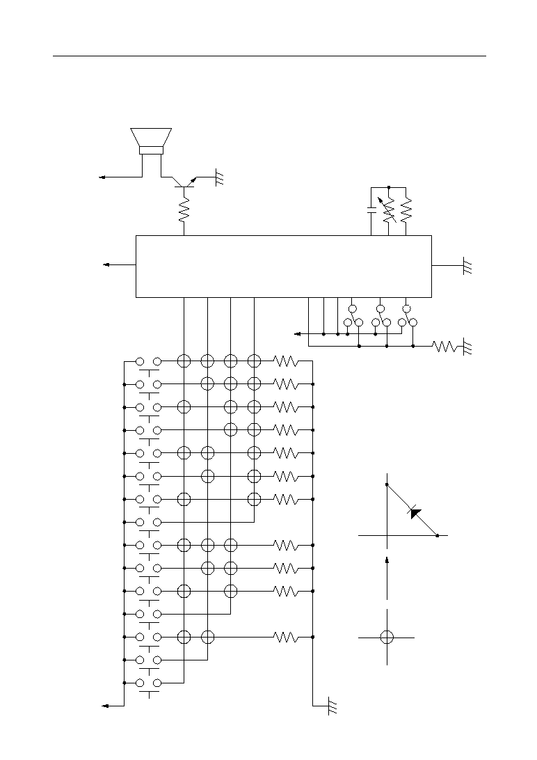
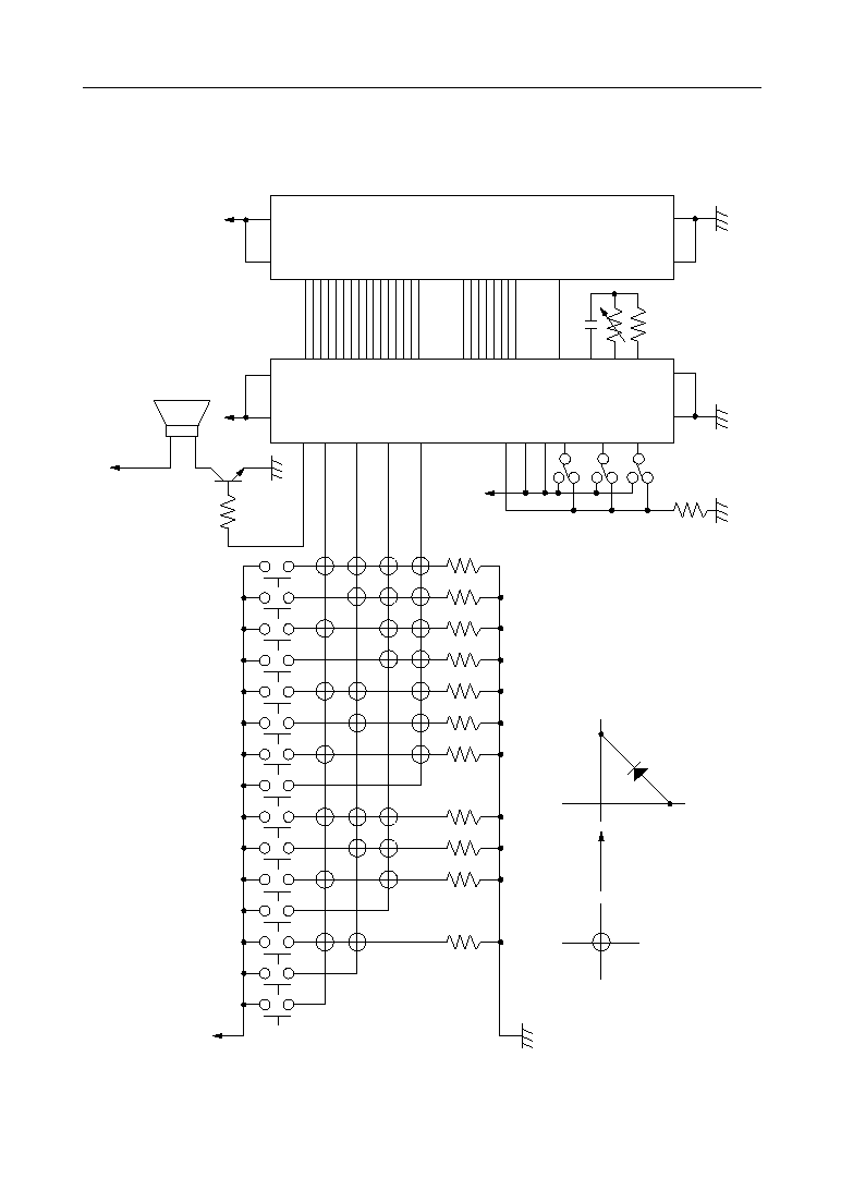
Application Circuit in Standalone Mode Supporting 15 Switch-Selected Phrases
18/45
° Semiconductor
MSM6650 Family
FEDL6650-03
SW0
AOUT
V
DD
TEST
RND
GND
OSC3
OSC2
OSC1
SW1
SW2
SW3
XT/
CR
A0
A1
A2
MSM6652/53/54/55/56
MSM6652A/53A/54A/55A/56A/58A
MSM66P54/P56
S4
S3
S2
S1
V
DD
Application Circuit in Standalone Mode Supporting Four Switch-Selected Words
Switches and Playback Addresses
S1
S2
S3
S4
0
0
0
0
0
0
0
0
0
0
0
0
0
0
0
1
0
0
1
0
0
1
0
0
1
0
0
0
01
02
04
08
A2
A1
A0
SW3
SW2
SW1
SW0
ADR
(MSM6652/53/54/55/56-xxx, MSM6652A/53A/54A/55A/56A/58A-xxx, MSM66P54/P56-xx)
19/45
° Semiconductor
MSM6650 Family
FEDL6650-03
1
2
3
4
5
6
7
8
9
10
11
12
13
14
15
SW0
SW1
SW2
SW3
RA15
DV
DD
XT/
CR
TEST1,3
RND
A0
A1
A2
DGND
OSC3
OSC2
OSC1
AOUT
RA0
V
CC
GND
V
PP
CE
A15
A0
D7
O7
D0
O0
CE
OE
MSM6650
MSM27C512
AV
DD
AGND
Application Circuit in Standalone Mode Supporting 15 Switch-Selected Phrases
(MSM6650)
20/45
° Semiconductor
MSM6650 Family
FEDL6650-03
SW0
SW1
SW2
SW3
RA18
DV
DD
XT/
CR
TEST2
RND
A0
A1
A2
DGND
OSC3
OSC2
OSC1
AOUT
RA0
V
DD
GND
V
PP
CE
A16
A0
D7
O7
D0
O0
OE
MSM6650
MSM27C101
AV
DD
AGND
V
DD
GND
V
PP
CE
A16
A0
O7
O0
OE
MSM27C101
V
DD
GND
V
PP
CE
A16
A0
O7
O0
OE
MSM27C101
V
DD
GND
V
PP
CE
A16
A0
O7
O0
OE
MSM27C101
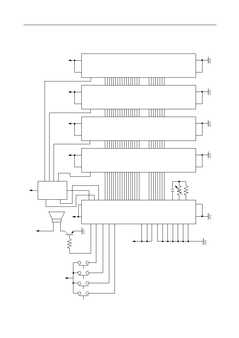
RA17
RA16
CE
2G
1B
1G
1Y3
1Y2
1Y1
1Y0
1A
74HC139
CPU
TEST3
TEST1
STBY
Application Circuit in Standalone Mode Supporting Four 1-Mbit EPROMs
(MSM6650)
21/45
° Semiconductor
MSM6650 Family
FEDL6650-03
MICROCONTROLLER INTERFACE MODE
FEATURES
Note: Actual voice ROM area is smaller by 22 Kbits.
∑ 4-bit ADPCM or 8-bit PCM sound generation
∑ Melody function
∑ Edit ROM function
∑ Two-channel mixing function
∑ Fade-out function via four-step sound volume attenuation
∑ Serial input or parallel input selectable
∑ Built-in beep tone of 0.5 kHz, 1.0 kHz, 1.3 kHz, or 2.0 kHz selectable with a specific code
∑ Sampling frequency of 4.0 kHz, 5.3 kHz, 6.4 kHz, 8.0 kHz, 10.6 kHz, 12.8 kHz, 16.0 kHz, or 32.0 kHz
(32 kHz sampling is not possible when using RC oscillation)
∑ Up to 127 phrases
∑ Built-in 12-bit D/A converter
∑ Built-in ≠40 dB/octave low-pass filter
∑ Standby function
∑ Package options:
18-pin plastic DIP (DIP18-P-300-2.54)
(Product name: MSM6652-xxxRS/MSM6653-xxxRS/
MSM6654-xxxRS/MSM6655-xxxRS/
MSM6656-xxxRS/MSM6652A-xxxRS/
MSM6653A-xxxRS/MSM6654A-xxxRS/
MSM6655A-xxxRS/MSM6656A-xxxRS/
MSM6658A-xxxRS)
24-pin plastic SOP (SOP24-P-430-1.27-K)
(Product name:MSM6652-xxxGS-K/MSM6653-xxxGS-K/
MSM6654-xxxGS-K/MSM6655-xxxGS-K/
MSM6656-xxxGS-K/MSM6652A-xxxGS-K/
MSM6653A-xxxGS-K/MSM6654A-xxxGS-K/
MSM6655A-xxxGS-K/MSM6656A-xxxGS-K/
MSM6658A-xxxGS-K/MSM66P54-01GS-K/
MSM66P54-02GS-K/MSM66P56-01GS-K/
MSM66P56-02GS-K)
20-pin plastic DIP (DIP20-P-300-2.54-W1) (Product name: MSM66P54-01RS/MSM66P54-02RS/
MSM66P56-01RS/MSM66P56-02RS)
64-pin plastic QFP (QFP64-P-1420-1.00-BK)(Product name: MSM6650GS-BK)
64-pin plastic SDIP (SDIP64-P-750-1.778) (Product name: MSM6650SS)
Device name
Data ROM
size
Maximum playback time (sec)
f
SAM
=4.0 kHz f
SAM
=6.4 kHz f
SAM
=8.0 kHz f
SAM
=16 kHz
MSM6650
64 Mbits (Max)
4194.3
2620.5
2096.4
1048.2
MSM6656, 6656A
2 Mbits
80.7
64.5
32.2
MSM6655, 6655A
1.5 Mbits
96.5
60.3
48.2
24.1
MSM6654, 6654A
1 Mbit
63.8
39.9
31.9
15.9
MSM6653, 6653A
544 Kbits
31.2
19.5
15.6
7.8
MSM6652, 6652A
288 Kbits
16.9
10.5
8.4
4.2
MSM66P54
1 Mbit
63.8
39.9
31.9
15.9
129.1
80.7
64.5
32.2
MSM6658A
4 Mbits
259.7
162.9
129.8
64.9
f
SAM
=32 kHz
524.1
16.1
12.0
7.9
3.9
2.1
7.9
32.4
MSM66P56
2 Mbit
129.1
80.7
64.5
32.2
16.1
22/45
° Semiconductor
MSM6650 Family
FEDL6650-03
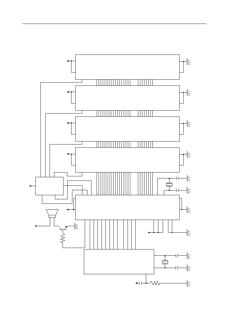
BLOCK DIAGRAMS
MSM6652/53/54/55/56-xxx
MSM6652A/53A/54A/55A/56A/58A-xxx
ROM
(Containing 22-Kbit Phrase Control
Table & Phrase Address Table)
16-
Bit
(MSM6652/52A)
17-
Bit
(MSM6653/53A)
17-
Bit
(MSM6654/54A)
18-
Bit
(MSM6655/55A)
18-
Bit
(MSM6656/56A)
19-
Bit
(MSM6658A)
Multiplexer
Address &
Command
Controller
7
ADPCM
Synthesizer
PCM
Synthesizer
12
8
12-Bit
DAC
LPF
AOUT
DATA
Controller
Melody
Generator
BEEP Tone
Generator
16-
Bit
(MSM6652/52A)
17-
Bit
(MSM6653/53A)
17-
Bit
(MSM6654/54A)
18-
Bit
(MSM6655/55A)
18-
Bit
(MSM6656/56A)
19-
Bit
(MSM6658A)
Address Counter
Timing Controller
GND
V
DD
RESET
I/O
Interface
OSC
I6/SD
I5/SI
I4
I3/PORT1
I2/PORT0
I1
I0
CH
NAR
XT
XT
(MSM6652/52A)
(MSM6653/53A)
(MSM6654/54A)
(MSM6655/55A)
(MSM6656/56A)
(MSM6658A)
288-Kbit
544-Kbit
1-Mbit
1.5-Mbit
2-Mbit
4-Mbit
ST
CMD
BUSY
23/45
° Semiconductor
MSM6650 Family
FEDL6650-03
MSM66P54/P56-xx
I6/SD
I5/SI
I4
I3/PORT1
I2/PORT0
I1
I0
NAR
XT
XT
RESET
V
DD
GND
AOUT
PGM
V
PP
Address &
Command
Controller
I/O
Interface
OSC
17-
Bit (MSM66P54-xx)
18-
Bit (MSM66P56-xx)
Multiplexer
17-
Bit (MSM66P54-xx)
18-
Bit (MSM66P56-xx)
Address Counter
Timing Controller
Program Circuit
1-Mbit OTP ROM (MSM66P54-xx)
2-Mbit OTP ROM (MSM66P56-xx)
(Containing 22-Kbit Phrase Control
Table & Phrase Address Table)
DATA
Controller
ADPCM
Synthesizer
PCM
Synthesizer
Melody
Generator
BEEP Tone
Generator
12-
Bit
DAC
LPF
12
8
7
BUSY
CMD
ST
CH
24/45
° Semiconductor
MSM6650 Family
FEDL6650-03
MSM6650
8-Bit LATCH
23-Bit Multiplexer
Address &
Switching
Controller
7
ADPCM
Synthesizer
PCM
Synthesizer
12
8
12-Bit
DAC
LPF
AOUT
DATA
Controller
Melody
Generator
BEEP Tone
Generator
23-Bit Address
Counter
Timing Controller
DGND
DV
DD
RESET
I/O
Interface
OSC
TEST1
I6/SD
I5/SI
I4
I3/PORT1
I2/PORT0
I1
I0
CE
RCS
BUSY
NAR
IBUSY
STANDBY
XT
XT
MCK
AV
DD
AGND
SERIAL
CPU
TEST2
RA22
RA0
D7
D0
CH
ST
CMD
25/45
° Semiconductor
MSM6650 Family
FEDL6650-03
PIN CONFIGURATION (TOP VIEW)
The MSM66P54/P56-xx has two more pins than the MSM6652-6658A while their pin configurations
are identical.
The additional two pins (V
PP
, PGM) of the MSM66P54/P56-xx may be open at playback after
completion of writing.
MSM6652-xxxGS-K, MSM6653-xxxGS-K,
MSM66P54-01/-02GS-K
MSM6654-xxxGS-K, MSM6655-xxxGS-K,
MSM66P56-01/-02GS-K
MSM6656-xxxGS-K, MSM6652A-xxxGS-K,
MSM6653A-xxxGS-K, MSM6654A-xxxGS-K,
MSM6655A-xxxGS-K, MSM6656A-xxxGS-K,
MSM6658A-xxxGS-K
MSM6652-xxxRS, MSM6653-xxxRS, MSM6654-xxxRS,
MSM66P54-01/-02RS
MSM6655-xxxRS, MSM6656-xxxRS, MSM6652A-xxxRS,
MSM66P56-01/-02RS
MSM6653A-xxxRS, MSM6654A-xxxRS, MSM6655A-xxxRS,
MSM6656A-xxxRS, MSM6658A-xxxRS
18-Pin Plastic DIP
1
2
3
4
5
6
7
8
9
18
17
16
15
14
13
12
11
10
CH
I6/SD
I5/SI
I4
RESET
NAR
AOUT
I3/PORT1
I2/PORT0
I1
I0
ST
CMD
XT
XT
MSM6652-6658A (Mask ROM)
24-Pin Plastic SOP
1
2
3
4
5
6
7
8
9
10
11
12
24
23
22
21
20
19
18
17
16
15
14
13
V
DD
XT
XT
NC
CMD
NC
NC
ST
I0
I1
I2/PORT0
I3/PORT1
GND
AOUT
NAR
NC
BUSY
NC
NC
RESET
CH
I6/SD
I5/SI
I4
BUSY
GND
V
DD
MSM6652-6658A (Mask ROM)
20-Pin Plastic DIP
1
2
3
4
5
6
7
8
9
10
20
19
18
17
16
15
14
13
12
11
CH
I6/SD
I5/SI
I4
V
PP
RESET
BUSY
NAR
AOUT
GND
PGM
I3/PORT1
I2/PORT0
I1
I0
ST
CMD
XT
XT
V
DD
MSM66P54/P56 (OTP)
24-Pin Plastic SOP
1
2
3
4
5
6
7
8
9
10
11
12
24
23
22
21
20
19
18
17
16
15
14
13
V
DD
XT
XT
NC
CMD
NC
PGM
ST
I0
I1
I2/PORT0
I3/PORT1
GND
AOUT
NAR
NC
BUSY
NC
V
PP
RESET
CH
I6/SD
I5/SI
I4
MSM66P54/P56 (OTP)
26/45
° Semiconductor
MSM6650 Family
FEDL6650-03
MSM6650
Product name: MSM6650GS-BK
,
1
NC
BUSY
NAR
NC
AOUT
AGND
DGND
AV
DD
DV
DD
XT
XT
MCK
CMD
ST
TEST1
CPU
SERIAL
IBUSY
NC
RA10
RA9
RA8
RA7
RA6
RA5
RA4
RA3
RA2
RA1
RA0
D7
D6
D5
D4
D3
D2
D1
NC
TEST2
RA22
RA21
RA20
RA19
RA18
RA17
RA16
RA15
RA14
RA13
RA12
RA11
STANDBY
I0
I1
I2/PORT0
I3/PORT1
I4
I5/SI
I6/SD
CH
RESET
CE
RCS
D0
2
3
4
5
6
7
8
9
10
11
12
13
14
15
16
17
18
19
20
21
22
23
24
25
26
27
28
29
30
31
32
33
34
35
36
37
38
39
40
41
42
43
44
45
46
47
48
49
50
51
52
53
54
55
56
57
58
59
60
61
62
63
64
NC : No connection
64-Pin Plastic QFP
27/45
° Semiconductor
MSM6650 Family
FEDL6650-03
20
1
2
3
4
5
6
7
8
9
10
11
12
13
14
15
16
17
18
19
CE
XT
MCK
CMD
ST
TEST1
CPU
SERIAL
IBUSY
NC
STANDBY
I0
I1
I2/PORT0
I3/PORT1
I4
I5/SI
I6/SD
CH
RESET
RA13
XT
DV
DD
AV
DD
DGND
AGND
AOUT
NAR
BUSY
NC
TEST2
RA22
RA21
RA20
RA19
RA18
RA17
RA16
RA15
RA14
45
64
63
62
61
60
59
58
57
56
55
54
53
52
51
50
49
48
47
46
21
22
23
24
25
26
27
28
29
30
31
32
44
43
42
41
40
39
38
37
36
35
34
33
RCS
RA12
D0
RA11
NC
RA10
D1
NC
D2
RA9
D3
RA8
D4
RA7
D5
RA6
D6
RA5
D7
RA4
RA0
RA3
RA1
RA2
NC : No connection
64-Pin Plastic SDIP
Product name: MSM6650SS
28/45
° Semiconductor
MSM6650 Family
FEDL6650-03
PIN DESCRIPTIONS
1.MSM6652/53/54/55/56-xxx, MSM6652A/53A/54A/55A/56A/58A-xxx
18-Pin plastic DIP
Symbol Type
Description
RESET
CMD
ST
Reset. The devices enter stanby status when a low level is input to this pin.
When RESET, oscillation stops. The AOUT output goes to ground and the IC
status is reinitialized.
This pin has an internal pull-up resistor.
I
I
I
CH
I6/SD
I5/SI
I
I
I
BUSY
O
NAR
O
Busy. Outputs a "L" level during playback and a "H" level when power is turned ON.
The CMD and ST inputs become effective when high. NAR indicates whether the
address bus (I0 through I6) is ready to accept another address. When high, it is
ready to accept. NAR goes high when power is turned ON.
AOUT
O
Analog Speech Output. D/A converter output or LPF output is selected by
entering the command.
Ceramic Oscillator Output. If an external clock is used, leave this pin open.
XT
O
Command Input and Option Control. This pin is used as command and
option input when CMD is at the high level with
ST low. If this pin is not used or
serial input is optioned, set this pin to "H" level. This pin has an internal pull-up
resistor.
Start. Speech playback starts at the fall of the
ST pulse. The I0 - I6 addresses
are latched at the rise of the
ST pulse. Input a ST pulse when NAR goes to the
high level for channels 1 and 2. This pin has an internal pull-up resistor.
Channel Control. Channel 1 is selected when the input is pulled high. Channel 2
is selected when the input is low. This pin has an internal pull-up resistor.
This pin is command and user-defined phrase input when parallel input is optioned.
This pin is serial data (command and address) input when serial input is optioned.
This pin is command and user-defined phrase input when parallel input is optioned.
This pin is used as serial clock input when serial input is optioned.
XT
I
Ceramic Oscillator Input. This pin has an internal 0.5 to 5 M
W feedback
resistor between XT and
XT. If an external clock is used, this is the clock input pin.
I4
I
This pin is command and user-defined phrase input when parallel input is optioned.
When serial input is optioned, set this pin to "L" level. This pin has an internal
pull-down resistor.
I3/PORT1
I/O
This pin is command and user-defined phrase input when parallel input is optioned.
When serial input is optioned, this pin is a port output. The port output is controlled
by entering external silence insertion code.
I2/PORT0
I/O
This pin is command and user-defined phrase input when parallel input is optioned.
When serial input is optioned, this pin is a port output. The port output is controlled
by entering external silence insertion code.
I0, I1
I
This pin is command and user-defined phrase input when parallel input is optioned.
When serial input is optioned, set this pin to "L" level. This pin has an internal
pull-down resistor.
Pin
5
13
14
4
3
2
6
7
8
12
11
1
18
17
15, 16
Ground pin.
GND
--
9
Power supply. Insert a 0.1µF ro more bypass capacitor between this pin and GND.
V
DD
--
10
29/45
° Semiconductor
MSM6650 Family
FEDL6650-03
2.MSM66P54/P56-xx
20-Pin plastic DIP
Symbol Type
Description
RESET
CMD
ST
Reset. The devices enter stanby status when a low level is input to this pin.
When RESET, oscillation stops. The AOUT output goes to ground and the IC
status is reinitialized.
This pin has an internal pull-up resistor.
I
I
I
CH
I6/SD
I5/SI
I
I
I
BUSY
O
NAR
O
Busy. Outputs a "L" level during playback and a "H" level when power is turned ON.
The CMD and ST inputs become effective when high. NAR indicates whether the
address bus (I0 through I6) is ready to accept another address. When high, it is
ready to accept. NAR goes high when power is turned ON.
AOUT
O
Analog Speech Output. D/A converter output or LPF output is selected by
entering the command.
Ceramic Oscillator Output. If an external clock is used, leave this pin open.
XT
O
Command Input and Option Control. This pin is used as command and
option input when CMD is at the high level with
ST low. If this pin is not used or
serial input is optioned, set this pin to "H" level. This pin has an internal pull-up
resistor.
Start. Speech playback starts at the fall of the
ST pulse. The I0 - I6 addresses
are latched at the rise of the
ST pulse. Input a ST pulse when NAR goes to the
high level for channels 1 and 2. This pin has an internal pull-up resistor.
Channel Control. Channel 1 is selected when the input is pulled high. Channel 2
is selected when the input is low. This pin has an internal pull-up resistor.
This pin is command and user-defined phrase input when parallel input is optioned.
This pin is serial data (command and address) input when serial input is optioned.
This pin is command and user-defined phrase input when parallel input is optioned.
This pin is used as serial clock input when serial input is optioned.
XT
I
Ceramic Oscillator Input. This pin has an internal 0.5 to 5 M
W feedback
resistor between XT and
XT. If an external clock is used, this is the clock input pin.
I4
I
This pin is command and user-defined phrase input when parallel input is optioned.
When serial input is optioned, set this pin to "L" level. This pin has an internal
pull-down resistor.
I3/PORT1
I/O
This pin is command and user-defined phrase input when parallel input is optioned.
When serial input is optioned, this pin is a port output. The port output is controlled
by entering external silence insertion code.
I2/PORT0
I/O
This pin is command and user-defined phrase input when parallel input is optioned.
When serial input is optioned, this pin is a port output. The port output is controlled
by entering external silence insertion code.
I0, I1
I
This pin is command and user-defined phrase input when parallel input is optioned.
When serial input is optioned, set this pin to "L" level. This pin has an internal
pull-down resistor.
Pin
6
14
15
5
4
3
7
8
9
13
12
2
19
18
16, 17
Ground pin.
GND
--
10
Power supply. Insert a 0.1µF ro more bypass capacitor between this pin and GND.
V
DD
--
11
Supply voltage for writing data to internal OTP ROM.
V
PP
--
1
PGM
I
Interface with voice analysis edit tools AR203 and AR204. Set to "L" level or leave
open during playback. This pin has an internal pull-down resistor.
20
30/45
° Semiconductor
MSM6650 Family
FEDL6650-03
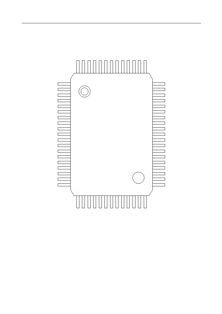
3.MSM6652/53/54/55/56-xxx, MSM6652A/53A/54A/55A/56A/58A-xxx, MSM66P54/P56-xx
24-Pin plastic SOP
Symbol Type
Description
RESET
CMD
ST
Reset. The devices enter stanby status when a low level is input to this pin.
When RESET, oscillation stops. The AOUT output goes to ground and the IC
status is reinitialized.
This pin has an internal pull-up resistor.
I
I
I
CH
I6/SD
I5/SI
I
I
I
BUSY
O
NAR
O
Busy. Outputs a "L" level during playback and a "H" level when power is turned ON.
The CMD and ST inputs become effective when high. NAR indicates whether the
address bus (I0 through I6) is ready to accept another address. When high, it is
ready to accept. NAR goes high when power is turned ON.
AOUT
O
Analog Speech Output. D/A converter output or LPF output is selected by
entering the command.
Ceramic Oscillator Output. If an external clock is used, leave this pin open.
XT
O
Command Input and Option Control. This pin is used as command and
option input when CMD is at the high level with
ST low. If this pin is not used or
serial input is optioned, set this pin to "H" level. This pin has an internal pull-up
resistor.
Start. Speech playback starts at the fall of the
ST pulse. The I0 - I6 addresses
are latched at the rise of the
ST pulse. Input a ST pulse when NAR goes to the
high level for channels 1 and 2. This pin has an internal pull-up resistor.
Channel Control. Channel 1 is selected when the input is pulled high. Channel 2
is selected when the input is low. This pin has an internal pull-up resistor.
This pin is command and user-defined phrase input when parallel input is optioned.
This pin is serial data (command and address) input when serial input is optioned.
This pin is command and user-defined phrase input when parallel input is optioned.
This pin is used as serial clock input when serial input is optioned.
XT
I
Ceramic Oscillator Input. This pin has an internal 0.5 to 5 M
W feedback
resistor between XT and
XT. If an external clock is used, this is the clock input pin.
I4
I
This pin is command and user-defined phrase input when parallel input is optioned.
When serial input is optioned, set this pin to "L" level. This pin has an internal
pull-down resistor.
I3/PORT1
I/O
This pin is command and user-defined phrase input when parallel input is optioned.
When serial input is optioned, this pin is a port output. The port output is controlled
by entering external silence insertion code.
I2/PORT0
I/O
This pin is command and user-defined phrase input when parallel input is optioned.
When serial input is optioned, this pin is a port output. The port output is controlled
by entering external silence insertion code.
Pin
17
5
8
16
15
14
20
22
23
3
2
13
12
11

31/45
° Semiconductor
MSM6650 Family
FEDL6650-03
Symbol Type
Description
I0, I1
I
This pin is command and user-defined phrase input when parallel input is optioned.
When serial input is optioned, set this pin to "L" level. This pin has an internal
pull-down resistor.
Pin
9, 10
Ground pin.
GND
--
24
Power supply. Insert a 0.1µF ro more bypass capacitor between this pin and GND.
V
DD
--
1
Supply voltage for writing data to internal OTP ROM.
V
PP
--
18
PGM
I
Interface with voice analysis edit tools AR761 and AR762. Set to "L" level or leave
open during playback. This pin has an internal pull-down resistor.
7
*
*
*
Pins for MSM66P54/56-xx only
32/45
° Semiconductor
MSM6650 Family
FEDL6650-03
4.MSM6650
64-Pin plastic QFP (64-Pin plastic SDIP)
Symbol Type
Description
RESET
CMD
ST
Reset. The devices enter stanby status when a low level is input to this pin.
When RESET, oscillation stops. The AOUT output goes to ground and the IC
status is reinitalized.
This pin has an internal pull-up resistor.
I
I
I
CH
I6/SD
I5/SI
I
I
I
BUSY
O
NAR
O
Busy. Outputs a "L" level during playback and a "H" level when power is turned ON.
The CMD and ST inputs become effective when high. NAR indicates whether the
address bus (I0 through I6) is ready to accept another address. When high, it is
ready to accept. NAR goes high when power is turned ON.
AOUT
O
Analog Speech Output. D/A converter output or LPF output is selected by
entering the command.
Ceramic Oscillator Output. If an external clock is used, leave this pin open.
XT
O
Command Input and Option Control. This pin is used as command and
option input when CMD is at the high level with
ST low. If this pin is not used or
serial input is optioned, set this pin to "H" level. This pin has an internal pull-up
resistor.
Start. Speech playback starts at the fall of the
ST pulse. The I0 - I6 addresses
are latched at the rise of the
ST pulse. Input a ST pulse when NAR goes to the
high level for channels 1 and 2. This pin has an internal pull-up resistor.
Channel Control. Channel 1 is selected when the input is pulled high. Channel 2
is selected when the input is low. This pin has an internal pull-up resistor.
This pin is command and user-defined phrase input when parallel input is optioned.
This pin is serial data (command and address) input when serial input is optioned.
This pin is command and user-defined phrase input when parallel input is optioned.
This pin is used as serial clock input when serial input is optioned.
XT
I
Ceramic Oscillator Input. This pin has an internal 0.5 to 5 M
W feedback
resistor between XT and
XT. If an external clock is used, this is the clock input pin.
I4
I
This pin is command and user-defined phrase input when parallel input is optioned.
When serial input is optioned, set this pin to "L" level. This pin has an internal
pull-down resistor.
I3/PORT1
I/O
This pin is command and user-defined phrase input when parallel input is optioned.
When serial input is optioned, this pin is a port output. The port output is controlled
by entering external silence insertion code.
I2/PORT0
I/O
This pin is command and user-defined phrase input when parallel input is optioned.
When serial input is optioned, this pin is a port output. The port output is controlled
by entering external silence insertion code.
I0, I1
I
This pin is command and user-defined phrase input when parallel input is optioned.
When serial input is optioned, set this pin to "L" level. This pin has an internal
pull-down resistor.
Pin
29 (19)
13 (3)
14 (4)
28 (18)
27 (17)
26 (16)
3 (57)
4 (58)
5 (59)
11 (1)
10 (64)
25 (15)
24 (14)
23 (13)
21, 22 (11, 12)
33/45
° Semiconductor
MSM6650 Family
FEDL6650-03
Symbol Type
Description
AGND
--
Analog ground pin.
MCK
O
Main clock output pin. Use MCK as a connection pin for the MSC1192, etc.
When the IC is in standby status, MCK is held high.
CPU
I
CPU Mode. Set to "H" level to select Microcontroller Interface Mode.
SERIAL
I
Serial/Parallel Interface Select. This input selects either the parallel or the
serial input interface. The serial input interface is selected with a high level; the
parallel input interface is selected with a low level.
CE
O
Chip Enable.
CE is a timing output pin to control read of external memory. This pin outputs
when
RCS is at the "L" level. This pin goes high impedance when RCS is at the "H" level.
RCS
I
Read Chip Select. The data bits D0-D7 are internally pulled down when
RCS is high.
DGND
--
Digital ground pin.
AV
DD
--
Analog power pin. Insert a 0.1
mF or more bypass capacitor between this pin and AGND.
DV
DD
--
Digital power pin. Insert a 0.1
mF or more bypass capacitor between this pin and DGND.
D0 - D7
I
External Memory Data Bus. Data is input when RCS is low. When RCS is high,
these pins become low due to internal pull-down resistors.
RA0 - RA22
O
External Memory Address. These are address pins for an external memory output
when
RCS is low. These pins become high impedance status if RCS is in "H" level.
TEST1, 2
I
Test. Set these pins to "H" level.
IBUSY
O
Outputs a "L" level during playback or when AOUT is at 1/2 V
DD
(except standby conversion)
STANDBY
O
Outputs a "L" level during which the device is oscillating.
Pin
6 (60)
12 (2)
16 (6)
17 (7)
30 (20)
31 (21)
7 (61)
8 (62)
9 (63)
32, 34-40
(22, 24-30)
41-63
(31-40, 42-54)
15, 64
(5, 55)
18 (8)
20 (10)
34/45
° Semiconductor
MSM6650 Family
FEDL6650-03
ABSOLUTE MAXIMUM RATINGS
Parameter
Symbol
Condition
Rating
Unit
Ta = 25∞C
--
(GND=0 V)
V
DD
≠0.3 to +7.0
V
Power supply voltage
V
IN
≠0.3 to V
DD+
0.3
V
Input voltage
T
STG
≠55 to +150
∞C
Storage temperature
RECOMMENDED OPERATING CONDITIONS
Parameter
Symbol
Condition
Range
Unit
(GND=0 V)
Typ.
Min.
Max.
4.096
3.5
4.5
MHz
V
DD
MSM6652-56, MSM6650,
MSM6652A-56A
2.4 to 5.5
V
MSM6658A, MSM66P54/P56
3.5 to 5.5
V
T
op
Operating temperature
--
≠40 to +85
∞C
f
OSC
Master clock frequency
--
Power supply voltage
35/45
° Semiconductor
MSM6650 Family
FEDL6650-03
ELECTRICAL CHARACTERISTICS
DC Characteristics
*1. Applied to RESET, CMD, ST, CH.
*2. Applied to MSM6652/53/54/55/56, MSM6652A/53A/54A/55A/56A/58A, MSM6650.
*3. Applied to MSM66P54/P56.
DC Characteristics
Note: Applied to RESET, CMD, ST, CH.
Parameter
Symbol
Condition
Min.
Unit
V
IH
V
IL
V
OH
V
OL
I
IH1
I
IH2
I
IL1
I
IL2
I
DD
High level input voltage
Low level input voltage
High level output voltage
Low level output voltage
High level input current 1
High level input current 2
Low level input current 1
Low level input current 2
Operating current
Standby current
D/A output relative accuracy
--
--
I
OH
=≠1 mA
I
OL
=2 mA
V
IH
=V
DD
Internal pull-down resistor
V
IL
=GND
Internal pull-up resistor
f
OSC
=4.096 MHz, No load
Ta=≠40
∞
C to +50
∞
C
Ta=≠40
∞
C to +85
∞
C
When D/A output selected
0.84•V
DD
--
4.6
--
--
30
≠10
≠200
--
--
--
--
V
V
V
V
mA
mA
mA
mA
mA
mA
mA
mV
Typ.
Max.
--
--
--
--
--
90
--
≠90
6
--
--
--
--
0.17•V
DD
--
0.4
10
200
--
≠30
10
10
30
40
(V
DD
=4.5 to 5.5 V, GND=0 V, Ta=≠40 to +85
∞
C)
*1
R
DAO
R
AOUT
R
LPF
D/A output impedance
LPF driving resisance
LPF output impedance
When D/A output selected
*2
When D/A output selected
*3
When LPF output selected
I
F
=100 mA
15
15
50
--
kW
kW
kW
kW
25
30
--
1
35
45
--
3
I
DS
|V
DAE
|
Parameter
Symbol
Condition
Min.
Unit
V
IH
V
IL
V
OH
V
OL
I
IH1
I
IH2
I
IL1
I
IL2
I
DD
High level input voltage
Low level input voltage
High level output voltage
Low level output voltage
High level input current 1
High level input current 2
Low level input current 1
Low level input current 2
Operating current
Standby current
D/A output relative accuracy
D/A output impedance
LPF driving resistance
LPF output impedance
--
--
I
OH
=≠1 mA
I
OL
=2 mA
V
IH
=V
DD
Internal pull-down resistor
V
IL
=GND
Internal pull-up resistor
f
OSC
=4.096 MHz, No load
Ta=≠40
∞
C to +50
∞
C
Ta=≠40
∞
C to +85
∞
C
When D/A output selected
When D/A output selected
When LPF output selected
I
F
=100 mA
0.84•V
DD
--
2.6
--
--
10
≠10
≠100
--
--
--
--
15
50
--
V
V
V
V
mA
mA
mA
mA
mA
mA
mA
mV
kW
kW
kW
(V
DD
=2.4 to 3.6 V, GND=0 V, Ta=≠40 to +85
∞
C)
Typ.
Max.
--
--
--
--
--
30
--
≠30
4
--
--
--
25
--
1
--
0.17•V
DD
--
0.4
10
100
--
≠10
7
5
20
20
35
--
3
(Note)
I
DS
|V
DAE
|
R
DAO
R
AOUT
R
LPF
36/45
° Semiconductor
MSM6650 Family
FEDL6650-03
APPLICATION CIRCUITS
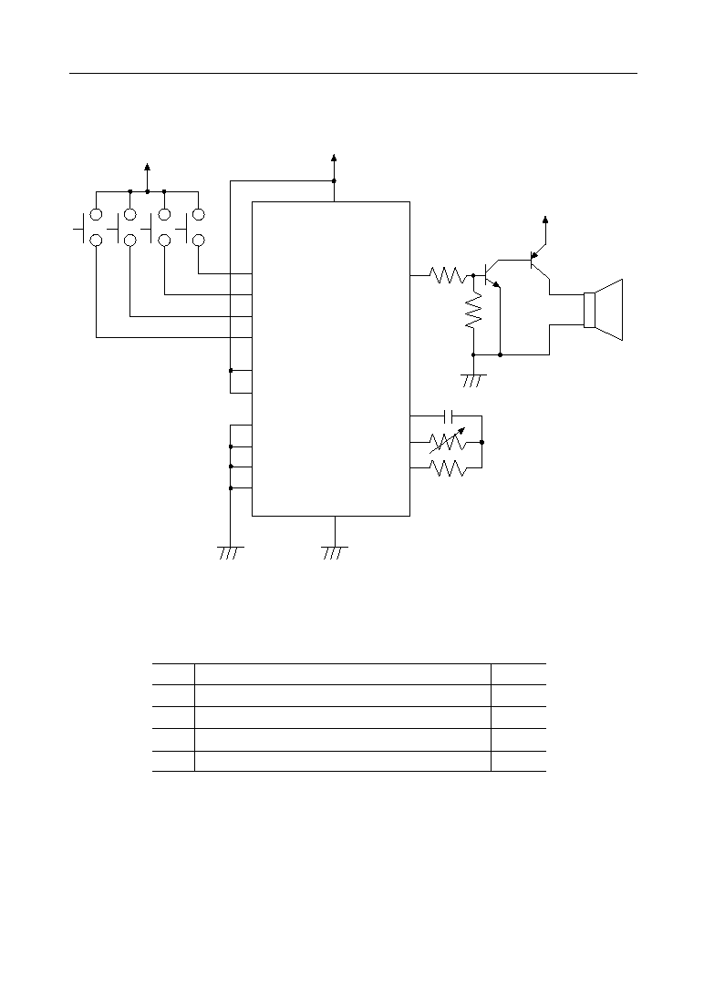
(MSM6652/53/54/55/56-xxx, MSM6652A/53A/54A/55A/56A/58A-xxx, MSM66P54/P56-xx)
P1.0
P1.1
P1.2
P2.0
P3.0
RESET
MSM83C154
CH
CMD
MSM6652/53/54/55/56
MSM6652A/53A/54A/55A/56A/58A
MSM66P54/P56
I6/SD
I5/SI
ST
RESET
NAR
XT
XT
GND
V
DD
AMP
PORT0
PORT1
AOUT
I4
I1
I0
Application Circuit in Serial Input Interface Mode
37/45
° Semiconductor
MSM6650 Family
FEDL6650-03
P2.0
P3.1
P2.2
P2.1
P3.0
RESET
MSM83C154
MSM6652/53/54/55/56
MSM6652A/53A/54A/55A/56A/58A
MSM66P54/P56
CH
CMD
ST
RESET
NAR
XT
XT
GND
V
DD
AMP
P1.6
I6
P1.0
I0
I5
I4
I3
I2
I1
P1.5
P1.4
P1.3
P1.2
P1.1
AOUT
Application circuit in Parallel Input Interface Mode
(MSM6652/53/54/55/56-xxx, MSM6652A/53A/54A/55A/56A/58A-xxx, MSM66P54/P56-xx)
38/45
° Semiconductor
MSM6650 Family
FEDL6650-03
Application Circuit in Microcontroller Interface Mode
Using Four 1-Mbit EPROMs (Serial Input Interface)
(MSM6650)
I5/SI
RA16
DV
DD
CH
DGND
XT
I6/SD
NAR
I0
MSM6650
AOUT
CMD
I1
I4
RCS
RA0
D7
D0
CE
RA18
RA17
1B
1A
V
DD
GND
V
PP
CE
OE
A16
A0
O7
O0
V
DD
GND
V
PP
CE
OE
A16
A0
O7
O0
V
DD
GND
V
PP
CE
OE
A16
A0
O7
O0
V
DD
GND
V
PP
CE
OE
A16
A0
O7
O0
1Y3
1Y2
1Y1
1Y0
2G
1G
74HC139
MSM27C101
MSM27C101
MSM27C101
MSM27C101
AV
DD
AGND
P2.0
P1.0
P1.1
P1.2
P3.0
RESET
MSM83C154
RESET
ST
TEST1
TEST2
CPU
SERIAL
XT
39/45
° Semiconductor
MSM6650 Family
FEDL6650-03
I2
RA16
DV
DD
CH
RCS
DGND
XT
XT
I1
I0
SERIAL
MSM6650
AOUT
ST
CMD
RA0
D7
D0
CE
RA18
RA17
1B
1A
V
DD
GND
V
PP
CE
OE
A16
A0
O7
O0
V
DD
GND
V
PP
CE
OE
A16
A0
O7
O0
V
DD
GND
V
PP
CE
OE
A16
A0
O7
O0
V
DD
GND
V
PP
CE
OE
A16
A0
O7
O0
1Y3
1Y2
1Y1
1Y0
2G
1G
74HC139
MSM27C101
MSM27C101
MSM27C101
MSM27C101
AV
DD
AGND
P2.0
P1.6
P1.5
P1.4
P1.3
P1.2
P1.1
P3.0
P2.1
P2.0
P3.1
P1.0
MSM83C154
RESET
RESET
TEST2
TEST1
I5/SI
I4
I3
I6/SD
NAR
CPU
Application Circuit in Microcontroller Interface Mode
Using Four 1-Mbit EPROMs (Parallel Input Interface)
(MSM6650)
40/45
° Semiconductor
MSM6650 Family
FEDL6650-03
(Unit : mm)
PACKAGE DIMENSIONS
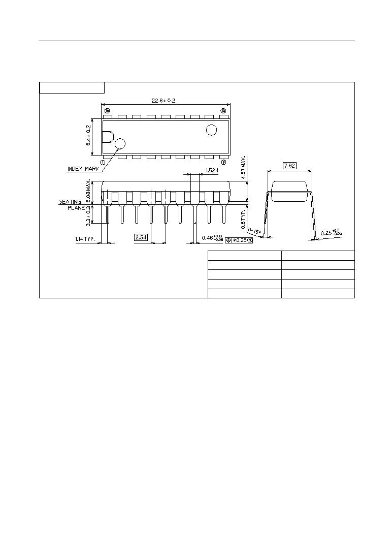
DIP18-P-300-2.54
Package material
Lead frame material
Pin treatment
Package weight (g)
Oki Electric Industry Co., Ltd.
Rev. No./Last Revised
Epoxy resin
42 alloy
Solder plating (5 mm)
1.30 TYP.
2/Dec. 11, 1996
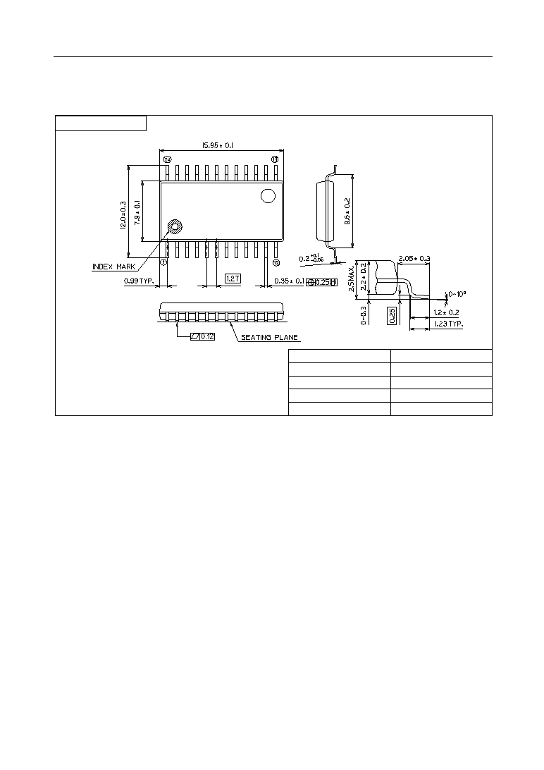
41/45
° Semiconductor
MSM6650 Family
FEDL6650-03
(Unit : mm)
Notes for Mounting the Surface Mount Type Package
The SOP, QFP, TSOP, TQFP, LQFP, SOJ, QFJ (PLCC), SHP, and BGA are surface mount type
packages, which are very susceptible to heat in reflow mounting and humidity absorbed in
storage. Therefore, before you perform reflow mounting, contact Oki's responsible sales person
on the product name, package name, pin number, package code and desired mounting conditions
(reflow method, temperature and times).
SOP24-P-430-1.27-K
Package material
Lead frame material
Pin treatment
Package weight (g)
Oki Electric Industry Co., Ltd.
Rev. No./Last Revised
Epoxy resin
42 alloy
Solder plating (5 mm)
0.58 TYP.
5/Oct. 13, 1998
Mirror finish
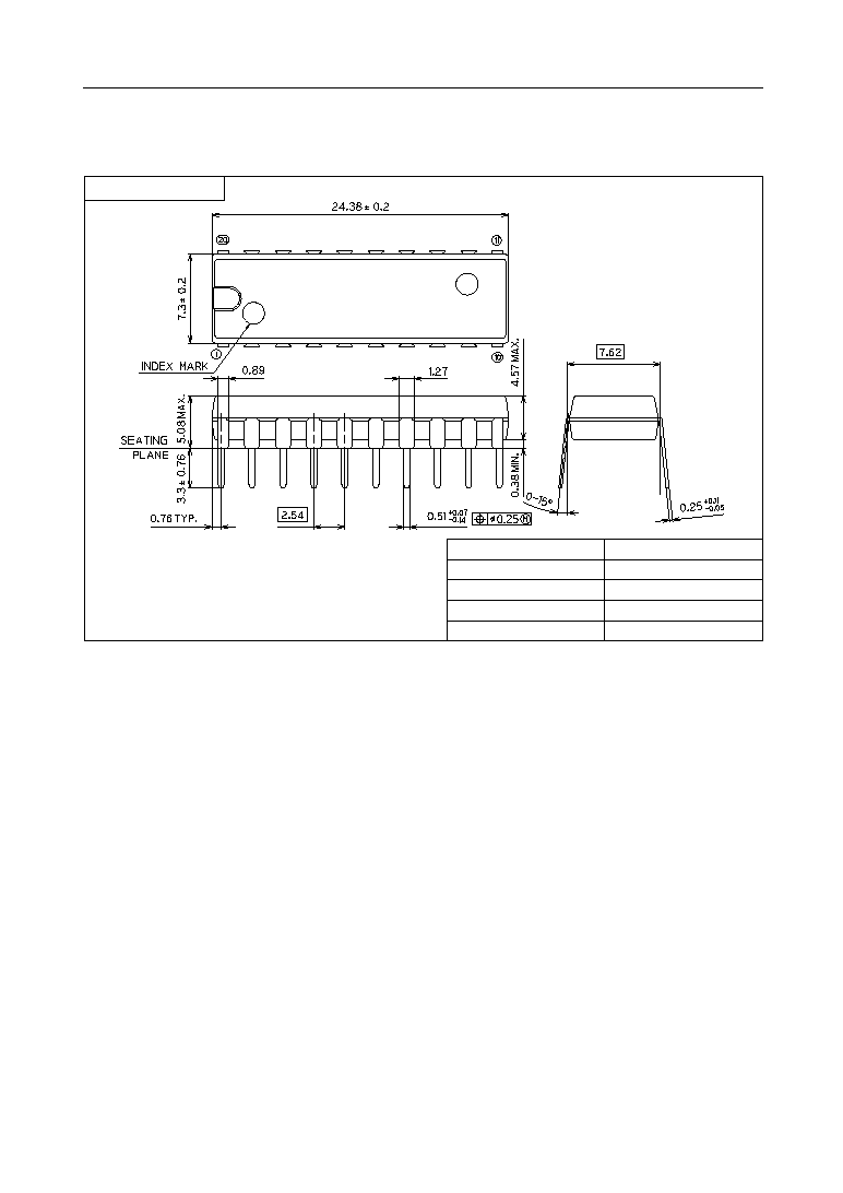
42/45
° Semiconductor
MSM6650 Family
FEDL6650-03
(Unit : mm)
DIP20-P-300-2.54-W1
Package material
Lead frame material
Pin treatment
Package weight (g)
Oki Electric Industry Co., Ltd.
Rev. No./Last Revised
Epoxy resin
42 alloy
Solder plating (5 mm)
1.50 TYP.
2/Dec. 11, 1996
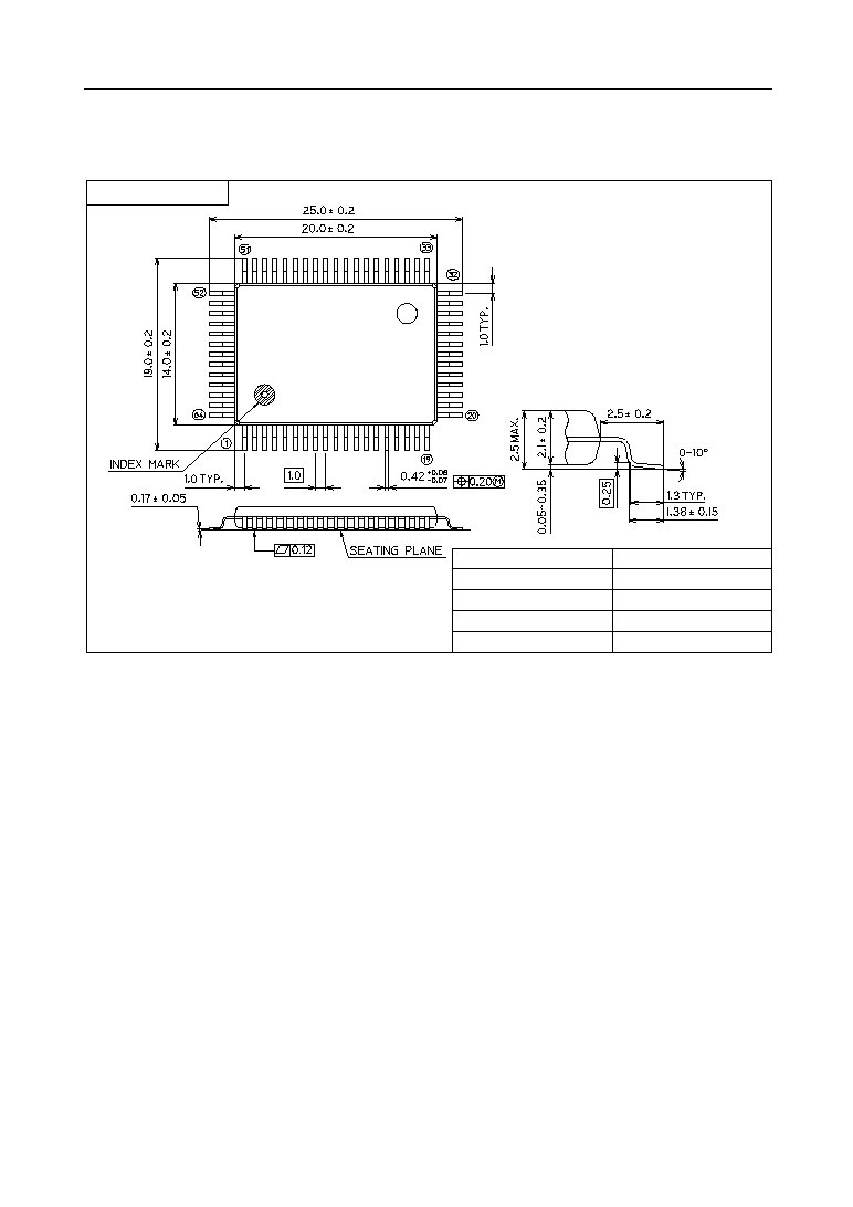
43/45
° Semiconductor
MSM6650 Family
FEDL6650-03
(Unit : mm)
Notes for Mounting the Surface Mount Type Package
The SOP, QFP, TSOP, TQFP, LQFP, SOJ, QFJ (PLCC), SHP, and BGA are surface mount type
packages, which are very susceptible to heat in reflow mounting and humidity absorbed in
storage. Therefore, before you perform reflow mounting, contact Oki's responsible sales person
on the product name, package name, pin number, package code and desired mounting conditions
(reflow method, temperature and times).
QFP64-P-1420-1.00-BK
Package material
Lead frame material
Pin treatment
Package weight (g)
Oki Electric Industry Co., Ltd.
Rev. No./Last Revised
Epoxy resin
42 alloy
Solder plating (5 mm)
1.25 TYP.
4/Nov. 28, 1996
Mirror finish
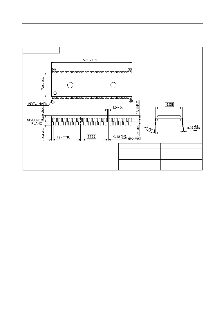
44/45
° Semiconductor
MSM6650 Family
FEDL6650-03
(Unit : mm)
SDIP64-P-750-1.778
Package material
Lead frame material
Pin treatment
Package weight (g)
Oki Electric Industry Co., Ltd.
Rev. No./Last Revised
Epoxy resin
Cu alloy
Solder plating (5 mm)
8.70 TYP.
2/Dec. 11, 1996

45/45
° Semiconductor
MSM6650 Family
FEDL6650-03
NOTICE
1.
The information contained herein can change without notice owing to product and/or
technical improvements. Before using the product, please make sure that the information
being referred to is up-to-date.
2.
The outline of action and examples for application circuits described herein have been
chosen as an explanation for the standard action and performance of the product. When
planning to use the product, please ensure that the external conditions are reflected in the
actual circuit, assembly, and program designs.
3.
When designing your product, please use our product below the specified maximum
ratings and within the specified operating ranges including, but not limited to, operating
voltage, power dissipation, and operating temperature.
4.
Oki assumes no responsibility or liability whatsoever for any failure or unusual or
unexpected operation resulting from misuse, neglect, improper installation, repair, alteration
or accident, improper handling, or unusual physical or electrical stress including, but not
limited to, exposure to parameters beyond the specified maximum ratings or operation
outside the specified operating range.
5.
Neither indemnity against nor license of a third party's industrial and intellectual property
right, etc. is granted by us in connection with the use of the product and/or the information
and drawings contained herein. No responsibility is assumed by us for any infringement
of a third party's right which may result from the use thereof.
6.
The products listed in this document are intended for use in general electronics equipment
for commercial applications (e.g., office automation, communication equipment,
measurement equipment, consumer electronics, etc.). These products are not authorized
for use in any system or application that requires special or enhanced quality and reliability
characteristics nor in any system or application where the failure of such system or
application may result in the loss or damage of property, or death or injury to humans.
Such applications include, but are not limited to, traffic and automotive equipment, safety
devices, aerospace equipment, nuclear power control, medical equipment, and life-support
systems.
7.
Certain products in this document may need government approval before they can be
exported to particular countries. The purchaser assumes the responsibility of determining
the legality of export of these products and will take appropriate and necessary steps at their
own expense for these.
8.
No part of the contents contained herein may be reprinted or reproduced without our prior
permission.
Copyright 2000 Oki Electric Industry Co., Ltd.