
1/24
° Semiconductor
MSM66585/586/587/P587/Q587
° Semiconductor
MSM66585/586/587/P587/Q587
Built-in 16 bit PWM and 8 bit A/D Converter, High-speed High-preformance 16 bit
Microcontroller
Preliminary
GENERAL DESCRIPTION
MSM66585/586/587 are high-performance CMOS 16-bit microcontrollers that integrate a 16-
bit CPU, ROM, RAM, 8-bit A/D converter, serial port, timers, and PWM. They also allow ROM
and RAM to be expanded externally.
The MSM66P587 is of OTP (One-Time PROM) version and the MSM66Q587 is of Flash EEPROM
version.
FEATURES
∑ Powerful instruction set
Instruction set superior in orthogonal matrics
8/16-bit arithmetic instructions
Multiply/divide instructions
Bit manipulation instructions
Bit logical operation instructions
ROM table reference instructions
∑ Abandant addressing modes
Register addressing
Page addressing
Pointer register indirect addressing
Stack addressing
Immediate addressing
∑ Minimum instruction cycle
100 ns at 20 MHz (4.5V-5.5V)
200 ns at 10 MHz (2.7V-5.5V)
∑ Program memory (ROM)
Internal:
64 KB (M66587/M66P587/M66Q587), 48 KB (M66585/586)
External: 1 MB, EA pin active
∑ Data memory (RAM)
Internal:
2 KB
External: 1022 KB
∑ I/O ports
Analog input-only port:
4 lines (test pins for M66585)
Input/output port:
Maximum 80 lines (40 lines with programmable pull-up)
∑ Timers
Free-running counter:
16-bit • 1
Realtime output:
16-bit • 2
General autoreload timer: 8-bit • 1
∑ 16-bit PWM
Input clock divider:
1 divider
∑ 8-bit serial port
Synchronous with BRG:
1 port
E2E1033 -27-Y6
This version: Jan. 1998
Previous version: Nov. 1996

2/24
° Semiconductor
MSM66585/586/587/P587/Q587
∑ A/D converter
8-bit resolution:
4 channels
∑ Interrupts
Non-maskable:
1 interrupt
Maskable:
9 internal, 4 external (12 vectors)
3-level priority
∑ ROM window function
∑ Standby modes
Halt mode
Stop mode
∑ Package
100-pin TQFP (TQFP100-P-1414-0.50-K) (Product name : MSM66585TS-K)
(Product name : MSM66586TS-K)
(Product name : MSM66587TS-K)
(Product name : MSM66P587TS-K)
(Product name : MSM66Q587TS-K)
3/24
° Semiconductor
MSM66585/586/587/P587/Q587
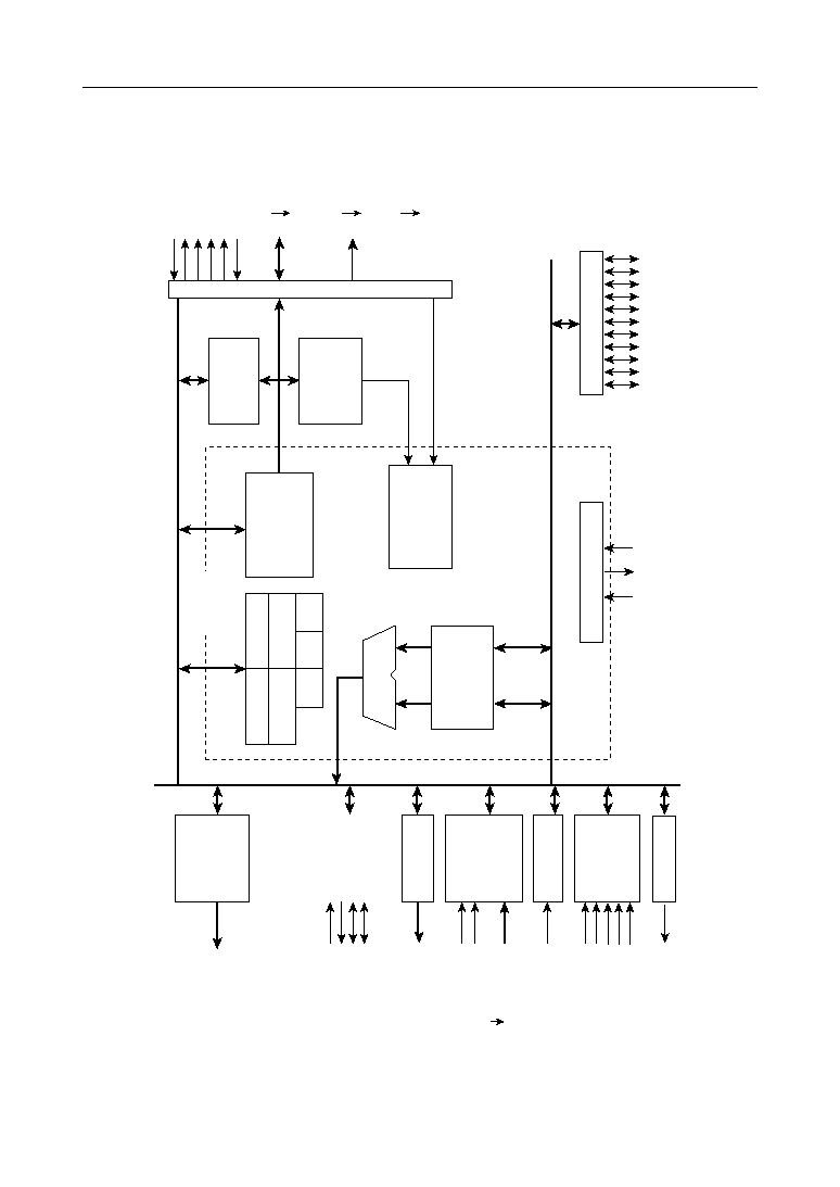
BLOCK DIAGRAM
SSP
LRB
PSW
PC
ALU
ALU Control
ACC
System Control
Instruction
Decoder
ROM
64 KB
Memory Control
Pointing R
Local R.
RAM
2 KB
EA
ALE/P5_5
PSEN/P5_4
RD/P7_1
WR/P7_0
WAIT/P7_2
AD0/P0_0
AD7/P0_7
A8/P1_0
A15/P1_7
A16/P9_0
A19/P9_3
Control
Registers
CPU Core
16-bit RTO/PWM
Timer
Serial Port
PWM
A to D
Converter
Event Timer
Interrupt
Peripheral
Port Control
*1
DSR TSR CSR
*2
RES
OSC1
OSC0
P12
P10
P9
P8
P7
P6
P5
P4
P2
P1
P0
Bus Port Control
P2_4/RT08
P2_5/RTO9
P6_2/RXD1
P6_3/TXD1
P6_4/RXC1
P6_5/TXC1
P7_4/PWM0
V
REF
AGND
AI0
AI3
P4_0/ETMCK
P6_0/INTO
P6_1/INT1
P12_2/INT2
P12_3/INT3
NMI
P7_3/CLKOUT
*1.
48KB for M66585 and M66586.
*2.
M66585 has no internal A/D converter.
4/24
° Semiconductor
MSM66585/586/587/P587/Q587
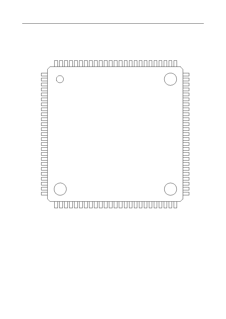
PIN CONFIGURATION (TOP VIEW)
75
1
76
77
78
79
80
81
82
83
84
85
86
87
88
89
90
91
92
93
94
95
96
97
98
99
100
50
49
48
47
46
45
44
43
42
41
40
39
38
37
36
35
34
33
32
31
30
29
28
27
26
ALE/P5_5
P5_4
PSEN
/P5_4
WR
/P7_0
RD
/P7_1
WAIT/P7_2
CLKOUT/P7_3
PWM0/P7_4
P7_5
P7_6
P7_7
GND
OSC1
OSC0
V
DD
EA
NMI
RES
P8_7
P8_6
P8_5
P8_4
P8_3
P8_2
P8_1
P8_0
P9_7
P2_0
P2_1
P2_2
P2_3
P2_4/RT08
P2_5/RT09
P2_6
P2_7
P10_0
P10_1
P10_2
P10_3
P10_4
P10_5
P10_6
P10_7
V
DD
GND
P6_0/INT0
P6_1/INT1
P6_2/RXD1
P6_3/TXD1
P6_4/RXC1
P6_5/TXC1
12_0
74
P9_4
73
P9_3/A19
72
P9_2/A18
71
P9_1/A17
70
P9_0/A16
69
GND
68
V
DD
67
P1_7/A15
66
P1_6/A14
65
P1_5/A13
64
P1_4/A12
63
P1_3/A11
62
P1_2/A10
61
P1_1/A9
60
P1_0/A8
59
P0_7/AD7
58
P0_6/AD6
57
P0_5/AD5
56
P0_4/AD4
55
P0_3/AD3
54
P0_2/AD2
53
P0_1/AD1
52
P0_0/AD0
51
2
P12_1
3
INT2/P12_2
4
INT3/P12_3
5
P12_4
6
P12_5
7
P12_6
8
P12_7
9
V
DD
10
*(V
DD
) V
REF
11
(GND) AGND
12
(TEST0) AI0
13
(TEST1) AI1
14
(TEST2) AI2
15
(TEST3) AI3
16
GND
17
V
DD
18
ETMCK/P4_0
19
P4_1
20
P4_2
21
P4_3
22
P4_4
23
P4_5
24
P4_6
25
P4_7
P9_6
P9_5
*
For MSM66585, pin name is in parentheses ( ).

5/24
° Semiconductor
MSM66585/586/587/P587/Q587
PIN DESCRIPTIONS
Symbol
Type
Description
P0_0-P0_7/
AD0-AD7
I/O
P1_0-P1_7/
A8-A15
I/O
P2_0-P2_3
P2_4-P2_5/
RT08-RT09
P2_6-P2_7
I/O
P4_0/ETMCK
P4_1-P4_7
I/O
P5_4/PSEN
P5_5/ALE
I/O
Port 0 is 8 input/output pins. Input or output can be specified for each bit with the
Port 0 Mode Register (P0IO). Pull-up resistors can be specified for each bit with the
Port 0 Pull-Up Register (P0PUP).
These pins also function as time-multiplexed address outputs and data input/output
pins (AD0-AD7) when accessing memory that has been expanded externally
(program or data memory).
After reset (by RES signal input, BRK instruction execution, or op code trap), P0 will
be high-impedance inputs.
Port 1 is 8 input/output pins. Input or output can be specified for each bit with the
Port 1 Mode Register (P1IO). Pull-up resistors can be specified for each bit with the
Port 1 Pull-Up Register (P1PUP).
P1_0-P1_7 also have a secondary function as input/output pins for internal operation.
Their secondary function can be set for each bit with the Port 1 Secondary Function
Control Register (P1SF). The input/output settings by P1IO will be ignored for pins
that have been set to the secondary function by P1SF.
These pins function as output pins for address A8-A15 when accessing program
memory or data memory that has been expanded externally. When the EA pin is low,
A8-A15 will be output regardless of P1SF settings.
After reset (by RES signal input, BRK instruction execution, or op code trap), P1 will
be high-impedance inputs.
P2_4 and P2_5 also have a secondary function as input/output pins for internal operation.
Their secondary function can be set for each bit with the Port 2 Secondary Function
Control Register (P2SF). The input/output settings of P2IO will be ignored for pins
that have been set to the secondary function by P2SF.
These pins output a previously set level when the value of Timer Registers 8 and 9
match a selected counter value.
After reset (by RES signal input, BRK instruction execution, or op code trap), P2 will
be high-impedance inputs.
Port 4 is 8 input/output pins. Input or output can be specified for each bit with the
Port 4 Mode Register (P4IO). Pull-up resistors can be specified for each bit with the
Port 4 Pull-Up Register (P4PUP).
P4_0 also has a secondary function as an input pin for internal operation. Its secondary
function can be set for the bit with the Port 4 Secondary Function Control Register (P4SF).
The input/output settings by P4IO will be ignored for pins that have been set to the
secondary function by P4SF.
This is the external clock input pin for the counter of a general 8-bit timer.
After reset (by RES signal input, BRK instruction execution, or op code trap), P4 will
be high-impedance inputs.
Port 5 is 2 input/output pins. Input or output can be specified for each bit with the
Port 5 Mode Register (P5IO).
P5_4 and P5_5 also have a secondary function as output pins for internal operation.
Their secondary function can be set for each bit with the Port 5 Secondary Function
Control Register (P5SF). The input/output settings of P5IO will be ignored for pins
that have been set to the secondary function by P5SF.
PSEN (P5_4):
This pin outputs the strobe signal for read operations when external program memory
is accessed. Operation will automatically switch to the secondary function when the
EA pin is low. This pin will be pulled up when both the EA pin and RESET pin are low.
ALE (P5_5):
This pin outputs the strobe for externally latching the lower 8 address bits output from
P0 when external memory is accessed. Operation will automatically switch to the
secondary function when the EA pin is low. This pin will be pulled up when both the
EA pin and RESET pin are low.
After reset (by RES signal input, BRK instruction execution, or op code trap), P5 will
be high-impedance inputs.