 | –≠–ª–µ–∫—Ç—Ä–æ–Ω–Ω—ã–π –∫–æ–º–ø–æ–Ω–µ–Ω—Ç: MSM66589 | –°–∫–∞—á–∞—Ç—å:  PDF PDF  ZIP ZIP |

1/27
° Semiconductor
MSM66589/66P589/66Q589
GENERAL DESCRIPTION
The MSM66589/66P589/66Q589 is a high-speed, high-performance 16-bit microcontroller that
employs OKI original nX-8/500S CPU core.
The MSM66589/66P589/66Q589 includes a 16-bit CPU, ROM, RAM, a 10-bit A/D converter,
serial ports, flexible timers, pulse-width modulator (PWM), and I/O ports.
The MSM66Q589 is a Flash EEPROM version.
FEATURES
∑ Program memory space
: 128K bytes
Internal ROM
: 96K bytes (MSM66589/66P589)
: 128K bytes (MSM66Q589)
∑ Data memory space
: 64K bytes
Internal RAM
: 4K bytes
∑ High-speed execution
Minimum instruction execution time : 100 nsec (@ 20 MHz)
∑ Built-in multiplier
∑ Powerful instruction set
: Instruction set superior in orthogonal matrix
8/16-bit data transfer instructions
8/16-bit arithmetic instructions
Multiplication and division operation instructions
Bit manipulation instructions
Bit logic instructions
ROM table reference instructions
∑ Abundant addressing modes
: Register addressing
Page addressing
Pointing register indirect addressing
Stack addressing
Immediate addressing
∑ I/O port
Analog input only ports
: 16 channels
Input-output ports
: 11 ports • 8 bits, 1 port • 6 bits
(Each bit can be configured to be an input or output)
∑ Flexible timers
Free run counters
: 19 bits • 1, 16 bits • 1
19-bit CAP with a divider
: 4
16-bit double buffer RTO
: 6
16-bit RTO/PWM
: 2
16-bit CAP/RTO
: 6
∑ 8-bit general timer
: 1
8-bit event counter
: 1
∑ 16-bit PWM
: 8
Input clock divider
: 1
∑ 8-bit serial ports
Preliminary
E2E1031-27-Y4
° Semiconductor
MSM66589/66P589/66Q589
OLMS-66K Series CMOS 16-Bit Microcontroller
This version: Jan. 1998
Previous version: Nov. 1996

2/27
° Semiconductor
MSM66589/66P589/66Q589
UART mode with BRG
: 1
Synchronous/UART switchable mode
with BRG
: 1
∑ 10-bit A/D converter
: 16 channels
∑ Transition detector
: 6
∑ Watchdog timer
: 1
∑ Interrupts
Non-maskable
: 1
Maskable
: Internal 47/external 2
(4-level priority can be set)
∑ ROM window function
∑ Standby modes
HALT mode
STOP mode
∑ Package:
128-pin plastic QFP (QFP128-P-2828-BK)
(Product name: MSM66589-•••GS-BK)
(Product name: MSM66P589-•••GS-BK)
(Product name: MSM66Q589GS-BK)
••• indicates the code number.
3/27
° Semiconductor
MSM66589/66P589/66Q589
BLOCK DIAGRAM
Serial Port
PWM
A/
D
Converter
Event Timer
Interrupt
Peripheral
WDT
SSP
LRB
PSW
PC
ALU
System Control
ROM *
96K bytes
RAM
4K bytes
EA ALE/P5_5 PSEN
/P5_4
RD
/P7_1
WR
/P7_0
WAIT/P7_2
AD0/P0_0
AD7/P0_7
A8/P1_0
A15/P1_7
A16/P9_0
O S C 0
Control Registers
CPU Core
P6_2/RXD1 P6_3/TXD1 P6_4/RXC1 P6_5/TXC1 P6_6/RXD0 P6_7/TXD0
P7_4/PWM0
P8_3/PWM7
AV
DD
V
REF
AGND AI0
AI15
P4_0/ETMCK P4_1/ECTCK
P4_2/TRNS0
P4_7/TRNS5
P6_0/INT0 P6_1/INT1 NMI
P7_3/CLKOUT
P 0
P 1
P 2
P 3
P 4
P 5
P 6
P 7
O E
O S C 1
R E S
P2_0/RTO4
P2_5/RTO9 P2_6/FTM10 P3_0/FTM11A P3_1/FTM11B
P3_3/FTM11D P3_4/CAP0
P3_7/CAP3 P10_0/RTO12 P10_1/RTO13 P10_2/FTM14
P10_5/FTM17
Flexible Timer
Transition Detector
P 8
P 9
P 1 0
P 1 1
Port Control
ALU Control
ACC
Instruction
Decoder
Memory Control
Pointing R.
Local R.
TSR
CSR
BUS PORT CONTROL
*
MSM66Q589 (Flash EEPROM version) contains 128K bytes Flash EEPROM.
4/27
° Semiconductor
MSM66589/66P589/66Q589
PIN CONFIGURATION (TOP VIEW)
96
95
94
93
92
91
90
89
88
87
86
85
84
83
82
81
80
79
78
77
76
75
74
73
72
71
70
69
68
67
66
65
1
2
3
4
5
6
7
8
9
10
11
12
13
14
15
16
17
18
19
20
21
22
23
24
25
26
27
28
29
30
31
32
P2_6/FTM10
P2_5/RTO9
P2_4/RTO8
P2_3/RTO7
P2_2/RTO6
P2_1/RTO5
P2_0/RTO4
V
DD
P9_7
P9_6
P9_5
P9_4
P9_3
P9_2
P9_1
P9_0/A16
P1_7/A15
P1_6/A14
P1_5/A13
P1_4/A12
P1_3/A11
P1_2/A10
P1_1/A9
P1_0/A8
GND
P0_7/AD7
P0_6/AD6
P0_5/AD5
P0_4/AD4
P0_3/AD3
P0_2/AD2
P0_1/AD1
TRNS3/P4_5
TRNS4/P4_6
TRNS5/P4_7
P5_0
P5_1
P5_2
P5_3
NMI
RES
EA
V
DD
AV
DD
V
REF
AI0
AI1
AI2
AI3
AI4
AI5
AI6
AI7
AI8
AI9
AI10
AI11
AI12
AI13
AI14
AI15
AGND
GND
INT0/P6_0
33
34
35
36
37
38
39
40
41
42
43
44
45
46
47
48
49
50
51
52
53
54
55
56
57
58
59
60
61
62
63
64
128
127
126
125
124
123
122
121
120
119
118
117
116
115
114
113
112
111
110
109
108
107
106
105
104
103
102
101
100
99
98
97
TRNS2/P4_4
TRNS1/P4_3
TRNS0/P4_2
ECTCK/P4_1
ETMCK/P4_0
P11_7
P11_6
P11_5
P11_4
P11_3
P11_2
P11_1
P11_0
V
DD
CAP3/P3_7
CAP2/P3_6
CAP1/P3_5
CAP0/P3_4
FTM11D/P3_3
FTM11C/P3_2
FTM11B/P3_1
FTM11A/P3_0
GND
P10_7
P10_6
FTM17/P10_5
FTM16/P10_4
FTM15/P10_3
FTM14/P10_2
RTO13/P10_1
RTO12/P10_0
P2_7
P6_1/INT1
P6_2/RXD1
P6_3/TXD1
P6_4/RXC1
P6_5/TXC1
P6_6/RXD0
P6_7/TXD0
GND
OSC0
OSC1
P5_5/ALE
P5_4/PSEN
P7_0/WR
P7_1/RD
P7_2/WAIT
P7_3/CLKOUT
P7_4/PWM0
P7_5/PWM1
P7_6/PWM2
P7_7/PWM3
V
DD
P8_0/PWM4
P8_1/PWM5
P8_2/PWM6
P8_3/PWM7
P8_4
P8_5
P8_6
P8_7
GND
OE
P0_0/AD0
128-Pin Plastic QFP (FLAT)

5/27
° Semiconductor
MSM66589/66P589/66Q589
PIN DESCRIPTION
Symbol
Type
Description
P0_0-P0_7/
AD0-AD7
P0: 8-bit input-output port. Each bit can be assigned to be an input or an output.
AD: When an external memory is used, these pins output the lower 8 bits of the address.
These pins also input or output the data.
I/O
P1_0-P1_7/
A8-A15
P1: 8-bit input-output port. Each bit can be assigned to input or output.
A: When an external memory is used, these pins output the upper 8 bits of the address.
I/O
P2_0-P2_5/
RTO4-RTO9
P2_6/FTM10
P2_7
P2: 8-bit input-output port. Each bit can be assigned to input or output.
RTO: Output pin for real time output
FTM10: Capture input pin or real-time output pin
I/O
P3_0-P3_3/
FTM11A-FTM11D
P3_4-P3_7/
CAP0-CAP3
P3: 8-bit input-output port. Each bit can be assigned to input or output.
FTM11A: Capture input pin or real-time output pin
FTM11B-D: 4-port real-time output pin
CAP : Capture input pin
I/O
P4_0/ETMCK
P4_1/ECTCK
P4_2-P4_7/
TRNS0-TRNS5
P4: 8-bit input-output port. Each bit can be assigned to input or output.
ETMCK: External clock input pin of 8-bit general timer
ECTCK: External clock input pin of 8-bit event counter
TRNS: Transition detector input pin
I/O
P5_0-P5_3
P5_4/PSEN
P5_5/ALE
P5: 6-bit input-output port. Each bit can be assigned to input or output.
PSEN: Strobe pulse output pin to fetch to external program memory
ALE: Timing pulse output pin to latch the lower 8 bits of the address output from port 0
when the CPU accesses the external memory
I/O
P6_0/INT0
P6_1/INT1
P6_2/RXD1
P6_3/TXD1
P6_4/RXC1
P6_5/TXC1
P6_6/RXD0
P6_7/TXD0
P6: 8-bit input-output port. Each bit can be assigned to input or output.
INT0, 1: External interrupt request input pin
RXD1 : SCI1 Receiver data input pin
TXD1 : SCI1 Transmitter data output pin
RXC1 : SCI1 Receiver circuit clock pin
TXC1 : SCI1 Transmitter circuit clock pin
RXD0 : SCI0 Receiver data input pin
TXD0 : SCI0 Transmitter data output pin
I/O
P7_0/WR
P7_1/RD
P7_2/WAIT
P7_3/CLKOUT
P7_4-P7_7/
PWM0-PWM3
P7: 8-bit input-output port. Each bit can be assigned to input or output.
WR: Write strobe output pin for external data memory
RD: Read strobe output pin for external data memory
WAIT: CPU wait request input pin when accessing external data memory
CLKOUT: Output pin to output clock pulse specified by PRPHF
PWM: PWM output pin
I/O
P8_0-P8_3/
PWM4-PWM7
P8_4-P8_7
P8: 8-bit input-output port. Each bit can be assigned to input or output.
PWM: PWM output pin
I/O
P9_0/A16
P9_1-P9_7
P9: 8-bit input-output port. Each bit can be assigned to input or output.
A16: When an external program memory is used, this pin outputs the MSB of the
address.
I/O
P10_0-P10_1/
RTO12-RTO13
P10_2-P10_5/
FTM14-FTM17
P10_6-P10_7
P10: 8-bit input-output port. Each bit can be assigned to input or output.
RTO: Output pin for real time output.
FTM: Capture input pin or real-time output pin
I/O
P11_0-P11_7
P11: 8-bit input-output port. Each bit can be assigned to input or output.
I/O

6/27
° Semiconductor
MSM66589/66P589/66Q589
PIN DESCRIPTION (Continued)
OE
When P0, P1, P2, P7_4-P7_7, and P8-P11 are in an output state and OE pin is "H"
level, P0, P1, P2, P7_4-P7_7, and P8-P11 go to a high-impedance state.
When P0, P1, P2, P7_4-P7_7, and P8-P11 are in an output state and OE pin is "L"
level, P0, P1, P2, P7_4-P7_7, and P8-P11 output "H" or "L" level.
However, when P0, P1, P2, P7_4-P7_7, and P8-P11 are in an input state, these
ports are not under the influence of OE pin.
I
NMI
Nonmaskable interrupt request input pin
I
RES
Low-active RESET input pin
I
EA
Normally set to "H" level. If set to "L" level, the program memory goes into
external access mode and accesses external program memory
I
V
DD
Power supply pin
I
GND
Ground pin
I
Symbol
Type
Description
AI0-AI15
Analog signal input pin for A/D converter
I
AV
DD
Power supply input pin for A/D converter
I
V
REF
Reference voltage input pin for A/D converter
I
AGND
GND input pin for A/D converter
I
OSC0
Basic clock oscillation pin
I
OSC1
O

7/27
° Semiconductor
MSM66589/66P589/66Q589
X1
X2
DP
USP
15
0
Code Segment Register
Table Segment Register
REGISTERS
Accumulator
Control Register (CR)
Program Status Word
PSW
Bit 15 : Carry flag (CY)
Bit 14 : Zero flag (ZF)
Bit 13 : Half carry flag (HC)
Bit 12 : Data descriptor (DD)
Bit 11 : Sign flag (S)
Bit 10 : Master interrupt priority flag (MIP)
Bit 9 : Overflow flag (OV)
Bit 8 : Master interrupt enable flag (MIE)
Bit 7 : Multiply and accumulate operation bank flag (MAB)*
Bit 6 : User flag (F1)
Bit 5 : Bank common base (BCB1)*
Bit 4 : Bank common base (BCB0)*
Bit 3 : User flag (F0)
Bit 2-0 : System control base 2-0 (SCB2-0)
* Bit 7 (MAB), Bit 5 (BCB1), and Bit 4 (BCB0) can be used
as the User flag.
PC
LRB
SSP
15
0
15
0
15
0
ACC
Pointing Register (PR)
Index Register 1
Index Register 2
Data pointer
User Stack Pointer
Program Counter
Local Register Base
System Stack Pointer
Segment Register
CSR
TSR
7
0

8/27
° Semiconductor
MSM66589/66P589/66Q589
Local Register
ER0
ER1
ER2
ER3
R1
R3
R5
R7
R0
R2
R4
R6
7
0 7
0
9/27
° Semiconductor
MSM66589/66P589/66Q589
SFR
Address [H]
Name
Abbreviated
Name (BYTE)
R/W
8/16
Operation
Reset
Status
0000
0001
0002
0003
0004
0005
0006
0007
00086
0009
000A
000B
000C6
000D6
000E
000F6
0010
0011
0012
0013
0014
00156
0016
0017
0018
0019
001A
001B
001C
001E
001F
0020
0021
0022
0023
0024
00256
00266
0027
System Stack Pointer
Local Register Base
Program Status Word
Accumulator
Table Segment Register
ROM Window Register
ROM Ready Control Register
RAM Ready Control Register
Stop Code Acceptor
Standby Control Register
Port 0 Data Register
Port 1 Data Register
Port 2 Data Register
Port 3 Data Register
Port 4 Data Register
Port 5 Data Register
Port 6 Data Register
Port 7 Data Register
Port 0 Mode Register
Port 1 Mode Register
Port 2 Mode Register
Port 3 Mode Register
Port 4 Mode Register
Port 5 Mode Register
Port 6 Mode Register
Port 7 Mode Register
Port 8 Data Register
Port 9 Data Register
Port 10 Data Register
Port 11 Data Register
TRNS Control Register
Transition Detector
Watchdog Timer
--
LRBL
LRBH
PSWL
PSWH
ACCL
ACCH
TSR
ROMWIN
ROMRDY
RAMRDY
STPACP
SBYCON
P0
P1
P2
P3
P4
P5
P6
P7
P0IO
P1IO
P2IO
P3IO
P4IO
P5IO
P6IO
P7IO
P8
P9
P10
P11
--
--
TRNSIT
WDT
SSP
LRB
PSW
ACC
--
--
--
--
--
P0P1
P2P3
P4P5
P6P7
P0P1IO
P2P3IO
P4P5IO
P6P7IO
P8P9
P10P11
TRNSCON
--
--
16
8/16
8
8
8/16
16
8
FFFF
Undefined
00
00
00
00
00
00
FF
FF
"0"
C8
00
00
00
00
00
C0
00
00
00
00
00
00
00
C0
00
00
00
00
00
00
F000
C0
Stop
001D6
Abbreviated
Name (WORD)
R/W
R/W
W
R/W
W
6 mark in the address column indicates that there is a nonexistent bit in its register.
--
10/27
° Semiconductor
MSM66589/66P589/66Q589
SFR (Continued)
Address [H]
Name
Abbreviated
Name (BYTE)
R/W
8/16
Operation
Reset
Status
0028
0029
002A
002B
002C6
002D6
002E
002F
0030
0031
00326
0033
0034
00356
0036
0037
00386
00396
003A6
003B
003C
003D
003E
003F
0040
0041
0042
0043
0044
0046
0047
0048
0049
004A
004B
004C
004D
004E
004F
Port 8 Mode Register
Port 10 Mode Register
A/D Interrupt Control Register
A/D Hardware Select Register
Port 1 Secondary Function Control Register
Port 3 Secondary Function Control Register
Port 4 Secondary Function Control Register
Port 5 Secondary Function Control Register
Port 6 Secondary Function Control Register
Port 7 Secondary Function Control Register
Port 8 Secondary Function Control Register
Port 9 Secondary Function Control Register
Port 10 Secondary Function Control Register
Interrupt Request Flag
Disable Register 0
Interrupt Request Flag
Disable Register1
Interrupt Request Register 0
Interrupt Request Register 1
Interrupt Enable Register 0
Interrupt Enable Register 1
Interrupt Priority Control
Register 00
Interrupt Priority Control
Register 01
Interrupt Priority Control
Register 10
Interrupt Priority Control
Register 11
P8IO
P10IO
P11IO
ADINTCON
ADHENCON
--
--
P3SF
P4SF
P5SF
P6SF
P7SF
P8SF
P9SF
P10SF
IRQD0L
IRQD0H
IRQD1L
IRQD1H
IRQ0L
IRQ0H
IRQ1L
IRQ1H
IE0L
IE0H
IE1L
IE1H
IP00L
IP00H
IP01L
IP01H
IP10L
IP10H
IP11L
IP11H
P8P9IO
P10P11IO
--
ADHSEL
--
--
--
--
--
IRQD0
IRQD1
IRQ0
IRQ1
IE0
IE1
IP00
IP01
IP10
IP11
8
8/16
8
8/16
00
00
C0
F0
0000
00
00
CF
00
00
F0
00
00
00
00
00
00
00
00
00
00
00
00
00
00
00
00
00
00
00
00
00
0045
Abbreviated
Name (WORD)
R/W
R/W
R/W
6 mark in the address column indicates that there is a nonexistent bit in its register.
Port 9 Mode Register
Port 11 Mode Register
A/D Hardware Select Enable Register
Port 2 Secondary Function Control Register
P9IO
P1SF
P2SF
--
--
--
--
--
---
16
00
00
00
80
00

11/27
° Semiconductor
MSM66589/66P589/66Q589
SFR (Continued)
Address [H]
Name
Abbreviated
Name (BYTE)
R/W
8/16
Operation
Reset
Status
0050
0051
0052
0053
0054
0055
0056
0057
0058
0059
005A
005B
005C
005D
005E
005F
0060
0061
0062
0063
0064
0065
0066
0067
0068
0069
006A
006B
006C
006E
006F
0070
0071
0072
0073
0074
0075
0076
0077
PWM Counter 0
PWC0 Buffer Register
--
PWC0
FFFF
006D
Abbreviated
Name (WORD)
R/W
6 mark in the address column indicates that there is a nonexistent bit in its register.
PWM Counter 1
--
PWC1
FFFF
PWM Counter 2
--
PWC2
FFFF
PWM Counter 3
--
PWC3
FFFF
PWM Counter 4
--
PWC4
FFFF
PWM Counter 5
--
PWC5
FFFF
PWM Counter 6
--
PWC6
FFFF
PWM Counter 7
--
PWC7
FFFF
16
R
--
PWC0BF
FFFF
PWC1 Buffer Register
PWC1BF
FFFF
PWC2 Buffer Register
PWC2BF
FFFF
PWC3 Buffer Register
PWC3BF
FFFF
PWC4 Buffer Register
PWC4BF
FFFF
PWC5 Buffer Register
PWC5BF
FFFF
PWC6 Buffer Register
PWC6BF
FFFF
PWC7 Buffer Register
PWC7BF
FFFF
PWR0 Buffer Register
PW0BF
0000
PWR1 Buffer Register
PW1BF
0000
PWR2 Buffer Register
PW2BF
0000
PWR3 Buffer Register
PW3BF
0000
--
--
--
--
--
--
--
--
--
--
--
12/27
° Semiconductor
MSM66589/66P589/66Q589
SFR (Continued)
Address [H]
Name
Abbreviated
Name (BYTE)
R/W
8/16
Operation
Reset
Status
0078
0079
007A
007B
007C
007D
007E
007F
0080
0081
0082
0083
0084
0085
0086
0087
0088
0089
008A
008B
008C
008D
008E
008F
0090
0091
0092
0093
0094
0096
0097
009A
009B
009C
009D
009E
009F
PWR4 Buffer Register
Timer Register 4
--
PW4BF
16
0000
0095
Abbreviated
Name (WORD)
R/W
6 mark in the address column indicates that there is a nonexistent bit in its register.
PWR5 Buffer Register
--
PW5BF
0000
PWR6 Buffer Register
--
PW6BF
0000
PWR7 Buffer Register
--
PW7BF
0000
Timer Register 0
--
TMR0
Undefined
Timer Register 1
--
TMR1
Undefined
Timer Register 2
--
TMR2
Undefined
Timer Register 3
--
TMR3
Undefined
R/W
--
TMR4
0000
Timer Register 5
TMR5
0000
Timer Register 6
TMR6
0000
Timer Register 7
TMR7
0000
Timer Register 8
TMR8
0000
Timer Register 9
TMR9
0000
Timer Register 10
TMR10
0000
Timer Register 11
TMR11
0000
Timer Register 12
TMR12
0000
Timer Register 13
TMR13
0000
Timer Register 14
TMR14
0000
Timer Register 15
TMR15
0000
--
--
--
--
--
--
--
--
--
--
--
R
0098
0099
13/27
° Semiconductor
MSM66589/66P589/66Q589
SFR (Continued)
Address [H]
Name
Abbreviated
Name (BYTE)
R/W
8/16
Operation
Reset
Status
00A0
00A1
00A2
00A3
00A4
00A5
00A6
00A7
00A8
00A9
00AA
00AB
00AC
00AD
00AE
00AF
00B06
00B16
00B26
00B36
00B46
00B56
00B66
00B76
00B8
00B96
00BA6
00BB6
00BC6
00BE6
00BF6
00C2
00C3
00C46
00C56
00C66
00C76
Timer Register 16
RTO Control Register 0
--
TMR16
0000
00BD6
Abbreviated
Name (WORD)
6 mark in the address column indicates that there is a nonexistent bit in its register.
Timer Register 17
--
TMR17
0000
TMR4 Buffer Register
--
TMR4BF
0000
TMR5 Buffer Register
--
TMR5BF
0000
TMR6 Buffer Register
--
TMR6BF
0000
TMR7 Buffer Register
--
TMR7BF
0000
TMR12 Buffer Register
--
TMR12BF
0000
TMR13 Buffer Register
--
TMR13BF
0000
16
RTOCON0
F8
Timer Counter 0
TM0
0000
Timer Counter 1
TM1
0000
TMR0 Low-order 3 Bits
--
Undefined
--
--
TMR0L
00C0
00C1
--
RTO Control Register 1
RTOCON1
F8
--
RTO Control Register 2
RTOCON2
F8
--
RTO Control Register 3
RTOCON3
F8
--
RTO Control Register 4
RTOCON4
FC
--
RTO Control Register 5
RTOCON5
FC
--
RTO Control Register 6
RTOCON6
F8
--
RTO Control Register 7
RTOCON7
F8
--
RTO Control Register 8
RTOCON8
00
--
RTO Control Register 9
RTOCON9
F8
--
RTO Control Register 10
RTOCON10
F8
--
RTO Control Register 11
RTOCON11
F8
--
RTO Control Register 12
RTOCON12
F8
--
RTO Control Register 13
RTOCON13
F8
--
RTO Control Register 14
RTOCON14
F8
--
Timer Counter 0 Low-order 3 bits
TM0L
--
1F
8
R/W
16
TMR1 Low-order 3 Bits
--
Undefined
TMR1L
TMR2 Low-order 3 Bits
--
Undefined
TMR2L
TMR3 Low-order 3 Bits
--
Undefined
TMR3L
8
R
14/27
° Semiconductor
MSM66589/66P589/66Q589
SFR (Continued)
Address [H]
Name
Abbreviated
Name (BYTE)
R/W
8/16
Operation
Reset
Status
00C86
00C96
00CA6
00CB6
00CC6
00CD6
00CE6
00CF6
00D0
00D1
00D2
00D3
00D4
00D5
00D6
00D7
00D8
00D9
00DA
00DB
00DC
00DD
00DE
00DF
00E06
00E16
00E2
00E36
00E4
00E6
00E76
00EA
00EB
00EC
00ED
00EE
00EF
Event Dividing Counter 0
EVDV0
--
C0
00E56
Abbreviated
Name (WORD)
6 mark in the address column indicates that there is a nonexistent bit in its register.
8
R/W
Capture Control Register
CAPCON
0000
--
00
PWM Control Register 0
--
00
--
CAPCON2
PWCON0
00E8
00E96
Undefined
A/D Control Register L
ADCONL
80
--
A/D Control Register H
ADCONH
80
--
Timer Control Register
TMCON
00
--
TM Setting Register 2
TMSEL2
C0
--
TM Setting Register
--
0000
TMSEL
TMR Mode Register
TMRMODE
00
--
TMR Mode Register 2
TMRMODE2
--
C0
8/16
(*1)
R/W
(*1)
PWM Control Register 1
--
00
PWCON1
PWM Control Register 2
--
00
PWCON2
PWM Control Register 3
--
00
PWCON3
8
R/W
Event Dividing Counter 1
EVDV1
--
C0
Event Dividing Counter 2
EVDV2
--
C0
Event Dividing Counter 3
EVDV3
--
C0
EVDV0 Buffer Register
EVDV0BF
--
C0
EVDV1 Buffer Register
EVDV1BF
--
C0
EVDV2 Buffer Register
EVDV2BF
--
C0
EVDV3 Buffer Register
EVDV3BF
--
C0
A/D Result Register 0
ADCR0
ADCR0W
A/D Result Register 1
ADCR1
ADCR1W
A/D Result Register 2
ADCR2
ADCR2W
A/D Result Register 3
ADCR3
ADCR3W
A/D Result Register 4
ADCR4
ADCR4W
A/D Result Register 5
ADCR5
ADCR5W
A/D Result Register 6
ADCR6
ADCR6W
A/D Result Register 7
ADCR7
ADCR7W
A/D Result Register 8
ADCR8
ADCR8W
A/D Result Register 9
ADCR9
ADCR9W
A/D Result Register 10
ADCR10
ADCR10W
A/D Result Register 11
ADCR11
ADCR11W
A/D Result Register 12
ADCR12
ADCR12W
A/D Result Register 13
ADCR13
ADCR13W
A/D Result Register 14
ADCR14
ADCR14W
A/D Result Register 15
ADCR15
ADCR15W
PWM RUN Register
--
00
PWRUN
16
8
16
8
Capture Control Register 2
15/27
° Semiconductor
MSM66589/66P589/66Q589
SFR (Continued)
Address [H]
Name
Abbreviated
Name (BYTE)
R/W
8/16
Operation
Reset
Status
00F0
00F1
00F2
00F3
00F4
00F5
00F6
00F7
00F86
00F9
00FA
00FB
00FC6
00FD6
00FE
00FF
PWM Interrupt Register 0
PWINTQ0
PWINTQ
00
Abbreviated
Name (WORD)
8
R/W
PWM Interrupt Register 1
PWINTQ1
00
PWM Interrupt Enable Register 0
PWINTE0
PWINTE
00
PWM Interrupt Enable Register 1
PWINTE1
00
SCI0 Transmit/Receive Buffer Register
S0BUF
--
Undefined
SCI0 Status Register
S0STAT
--
00
SCI1 Transmit/Receive Buffer Register
S1BUF
--
Undefined
SCI1 Status Register
S1STAT
--
00
General-purpose 8-bit Timer Control Register
GTMCON
--
8-bit Event Counter
GEVC
--
General-purpose 8-bit Timer Counter
GTMC
--
General-purpose 8-bit Timer Register
GTMR
--
Event Control Register
EVNTCONL
--
EVNTCONH
--
Emulator Use Area
* Note 3
8/16
30
00
00
00
88
88
0100
01016
0102
0103
0104
0105
0106
01076
01086
01096
010A
010B
010C
010D
010E
010F
0110
0111
01126
01136
01146
0115
0116
0117
Memory Size Acceptor
MEMSACP
--
"0"
8
W
Memory Size Control Register
MEMSCON
--
FC
Peripheral Control Register
PRPHF
--
(*3)
NMI Control Register
NMICON
--
External Interrupt Control Register
EXICON
--
SCI0 Timer
--
S0TM
SCI0 Timer Control Register
S0CON
--
SCI0 Transmit Control Register
ST0CON
--
SCI0 Receive Control Register
SR0CON
--
FC or 7C
00
8
8
16
0000
02
8A
1A
R/W
R/W
R/W
16/27
° Semiconductor
MSM66589/66P589/66Q589
Address [H]
Name
Abbreviated
Name (BYTE)
R/W
8/16
Operation
Reset
Status
0118
0119
011A6
011B6
011C6
011E6
011F6
0122
0123
0124
0125
0126
0127
011D
Abbreviated
Name (WORD)
0120
0121
SCI1 Timer
--
0000
S1TM
SCI1 Timer Control Register
S1CON
02
--
SCI1 Transmit Control Register
ST1CON
88
--
SCI1 Receive Control Register
SR1C0N
08
--
TBC Clock Dividing Counter
TBCKDVC
F0
--
TBC Clock Dividing Register
TBCKDVR
--
F0
R/W
8
8
16
R/W
R
6 mark in the address column indicates that there is a nonexistent bit in its register.
*1
*2
*3
The 8/16 bit operation for the ADCR items is a special word manipulation. If a byte access is made, high-order 8 bits of
the A/D Result register are accessed, and if a word access is made, the 10-bit contents of the A/D Result register are
accessed.
Data can be written in the even number A/D Result registers and the odd number A/D Result registers separately.
When data is first written in the A/D Result register 0 (ADCR0), data is also written in other even number A/D Result
registers at a time. When data is first written in the A/D Result register 1 (ADCR1), data is also written in other odd A/D
Result registers at a time.
Do not access the emulator use area.
The initial values of PRPHF (SFR=107H) are as follows:
At reset by RES pin: VBFF (bit 6) is "1"; CKOUT1 (bit 1) and CKOUT0 (bit 0) are "0".
At reset by WDT and BRK instructions and operation code trap: VBFF (bit 6) holds the value just before reset; CKOUT1
(bit 1) and CKOUT0 (bit 0) are "0".
In both cases, the OE pin status is read for OERD (bit 7).
SFR (Continued)
17/27
° Semiconductor
MSM66589/66P589/66Q589
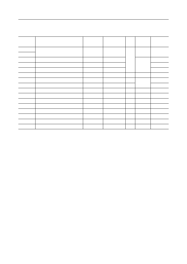
∑ Direct data addressing
ADDRESSING MODES
The MSM66589/66P589/66Q589 provides independent 64K-byte data and 128K-byte program
spaces with various types of addressing modes. These modes are shown below for both RAM
(for data space) and ROM (for program space).
RAM Addressing Mode (for data space)
∑ Register addressing
∑ Page addressing
a) sfr page
b) Fixed page
c) Current page
INC USP
Example
USP
L A, sfr IRQ0
Example
SFR
0000H
0040H
ST A, fix 0C0H
Example
RAM
0200H
02C0H
ROR off 078H
Example
RAM
xx00H
xx78H
CLR dir 780H
Example
RAM
0700H
0780H
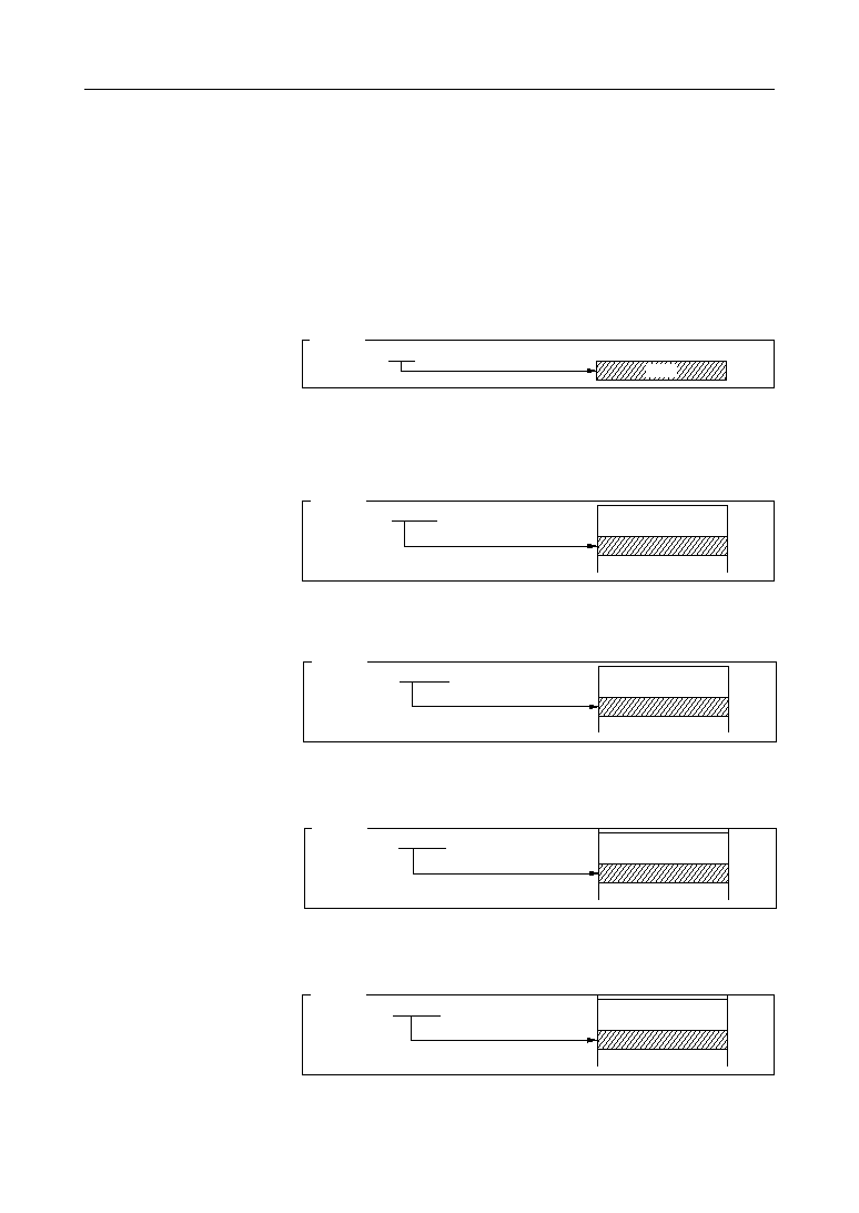
18/27
° Semiconductor
MSM66589/66P589/66Q589
f) X1 indirect with 8-bit register (A, R0) displacement
XCHG A, [DP]
RAM
DP
Example
ADD A, [DP+]
RAM
DP
After access, DP is incremented by 2.
Example
SUB A, [DP-]
RAM
DP
After access, DP is decremented by 2.
Example
AND A, 12[DP]
RAM
DP
≠64 to +63
Example
XOR A, 1234H[X1]
RAM
X1
0-65535
Example
OR A, [X1+A]
RAM
X1
AL
Example
∑ Pointing register indirect addressing
a) DP/X1 indirect
b) Post increment DP indirect
c) Post decrement DP indirect
d) DP/USP indirect with 7-bit displacement
e) X1/X2 indirect with 16-bit base

19/27
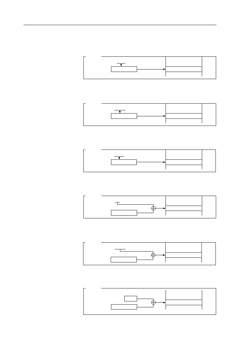
° Semiconductor
MSM66589/66P589/66Q589
RB sbaoff 2E9H.7
RAM
••C0H
••E9H
Example
SB sbafix 2D1H.3
RAM
02C0H
02D1H
Example
LC A, 5678H
ROM
5678H
Example
MOV SSP, #7FFH
ROM
Address
xxxxH
Example
∑ Special bit area addressing
a) Fixed page SBA area (02C0H to 02FFH)
b) Current page SBA area (••C0H to ••FFH)
ROM Addressing Mode (for program space)
∑
Immediate addressing
∑ Table data addressing
TSR specifies the address segment.
a) Direct
b) RAM addressing indirect
CMPC A, [USP]
ROM
USP
Example
c) RAM addressing indirect with 16-bit base
LC A, 1234H[ER0]
ROM
ER0
0-65535
RAM
Example
20/27
° Semiconductor
MSM66589/66P589/66Q589
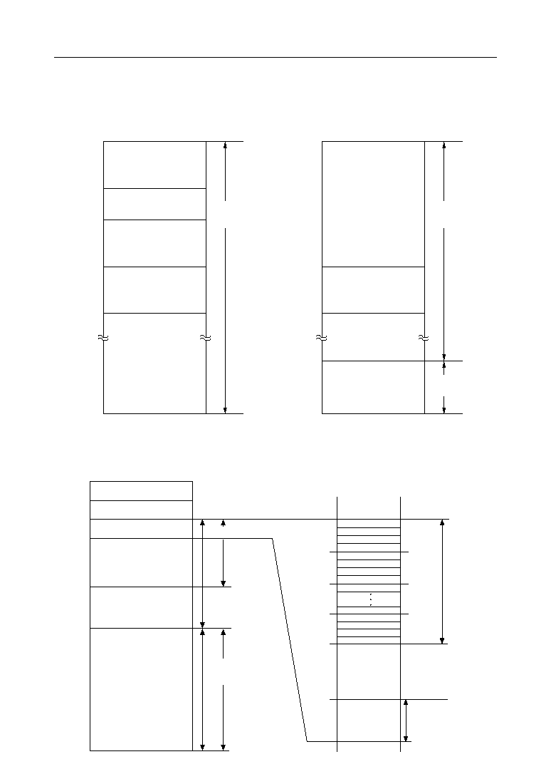
MEMORY MAP
Program Memory Space
17FFH
1800H
FFFFH
0FFFH
1000H
0069H
006AH
0049H
004AH
0000H
Vector table area
(74 bytes)
VCAL table area
(32 bytes)
ACAL area
(2K bytes)
ACAL area
(2K bytes)
17FFH
1800H
FFFFH
0FFFH
1000H
0000H
External
ROM area *
7FFFH
8000H
Internal
ROM area
Segment 0
Segment 1
Internal
ROM area
*
For MSM66Q589 (Flash EEPROM version), 8000H to 0FFFFH in Segment 1 are in the internal
ROM area.
Data Memory Space
0000H
00FFH
0100H
01FFH
0200H
02FFH
0300H
09FFH
0A00H
11FFH
1200H
FFFFH
SFR Area
Expanded SFR Area
FIX Area
Internal RAM Area
Area where
local
register
can be set
External Memory Area
Area where ROM
window can be set
01FFH
0200H
0208H
0210H
0238H
0240H
0300H
02C0H
X1
X2
DP
USP
X1
X2
DP
USP
X1
USP
X1
X2
DP
USP
Expanded
SFR Area
SBA Area
(64 bytes)
SCB=0
SCB=1
SCB=7
Pointing
Register Set
Area where SB, RB,
JBS, and JBR
instructions can be
performed in shorter
byte count.
. . . .
. . . . .

21/27
° Semiconductor
MSM66589/66P589/66Q589
ABSOLUTE MAXIMUM RATINGS
Parameter
Symbol
Unit
Rating
Condition
Digital Power Supply Voltage
Input Voltage
Output Voltage
Analog Power Supply Voltage
Analog Reference Voltage
Analog Input Voltage
Power Dissipation
Storage Temperature
V
DD
≠0.3 to 7.0
Ta=85∞C
V
I
≠0.3 to V
DD
+0.3
V
O
≠0.3 to V
DD
+0.3
V
AV
DD
≠0.3 to V
DD
+0.3
V
REF
≠0.3 to AV
DD
+0.3
V
AI
≠0.3 to V
REF
P
D
GND=AGND=0 V
Ta = 25∞C
Per package
Per output
mW
50
≠50 to +150
∞C
T
STG
--
(Ta=25∞C)
855
RECOMMENDED OPERATING CONDITIONS
Digital Power Supply Voltage
Analog Power Supply Voltage
Analog Reference Voltage
Analog Input Voltage
Memory Hold Voltage
Operating Frequency
Fan Out
V
DD
4.5 to 5.5
AV
DD
4.5 to 5.5
V
REF
AV
DD
≠0.3 to AV
DD
V
V
AI
AGND to V
REF
V
DDH
2.0 to 5.5
f
OSC
0 to 20
MHz
N
TTL load
P0, P5_4, P5_5, P7_0, P7_1
P1 to P11 (except P5_4,P5_5, P7_0, P7_1)
≠40 to +85
∞C
20
2
1
f
OSC
£20 MHz
V
DD
=AV
DD
f
OSC
=0 Hz
V
DD
=5 V±10%
Ambient Temperature
Ta
--
MOS load
Parameter
Symbol
Unit
Range
Condition
--
--
--
22/27
° Semiconductor
MSM66589/66P589/66Q589
ELECTRICAL CHARACTERISTICS
DC Characteristics (Preliminary)
Parameter
Symbol
Unit
Condition
Min.
Typ.
Max.
H Level Input Voltage
H Level Input Voltage
V
µA
µA
µA
µA
pF
mA
mA
mA
V
IH
V
IL
V
OH
≠
≠
I
OH
=≠400 mA
I
OH
=≠200 mA
I
OL
=3.2 mA
I
OL
=1.6 mA
V
I
=V
DD
/0 V
V
O
=V
DD
/0 V
f=1 MHz, Ta=25∞C
V
DD
=2 V, Ta=25∞C*
f
OSC
=20 MHz
No load
*
A/D in operation
A/D stopped
V
O
=2.4 V
≠
2.2
V
DD
+0.3
(V
DD
=5 V±10%, Ta=≠40 to +85∞C)
≠
0.80V
DD
V
DD
+0.3
≠
V
DD
≠0.4
≠
≠
V
DD
≠0.4
≠
≠
≠2
≠
≠
≠1
≠
≠
10
≠
≠
5
5
7
0.2
1
≠
≠
≠
≠
≠
0.4
≠
≠
≠
≠
≠
≠
≠
≠
0.4
1/≠1
1/≠250
15/≠15
≠
≠
≠
≠
≠
≠
≠
≠
≠
≠
≠
≠
±2
6
10
10
100
≠
≠0.3
0.8
≠
≠0.3
0.2V
DD
1
2, 4, 5, 6, 7
2, 4, 5, 6, 7
L Level Input Voltage
L Level Input Voltage
1, 4
H Level Output Voltage
2
H Level Output Voltage
I
OH
1, 4
H Level Output Current
2
1, 4
2
H Level Output Current
I
OL
I
REF
I
LO
C
I
C
O
L Level Output Current
Input Capacitance
L Level Output Current
I
DDS
I
DDH
Output Capacitance
Analog Reference Current
Current Consumption
(in STOP mode)
Current Consumption
(in HALT mode)
I
DD
Current Consumption
1, 2, 4
Output Leakage Current
V
OL
1, 4
L Level Output Voltage
2
L Level Output Voltage
1
I
IH
/I
IL
5
7
Input Leakage Current
Input Current
Input Current
3, 6
45
80
1. Applied to P0
2. Applied to P1 to P11 (except P5_4, P5_5, P7_0, P7_1)
3. Applied to A
IN
4. Applied to P5_4, P5_5, P7_0, P7_1
5. Applied to RES
6. Applied to EA, OE, NMI
7. Applied to OSC0
*
Ports for input pins are V
DD
or GND, otherwise no load.
23/27
° Semiconductor
MSM66589/66P589/66Q589
Parameter
Symbol
Condition
Min.
Max.
Unit
Clock (OSC) pulse width
t
¯W
--
25
--
nsec
ALE pulse width
t
AW
2t
¯W
≠10
--
RD pulse delay time
t
RAD
t
¯W
≠10
t
¯W
+10
WR pulse delay time
t
WAD
t
¯W
≠10
t
¯W
+10
Low-order address set-up time
t
ALS
2t
¯W
≠10
2t
¯W
+10
Low-order address hold time
t
ALH
C
L
=50 pF
t
¯W
≠10
t
¯W
+10
High-order address hold time
t
AHH
t
¯W
≠0
t
¯W
+10
Data set-up time
t
DD
t
ALH
≠0
t
ALH
+10
Data hold time
t
DH
t
¯W
≠10
t
¯W
+10
(V
DD
=5 V±10%, Ta=≠40 to +85∞C)
RD pulse width
t
RW
2t
¯W
≠10
--
WR pulse width
t
WW
2t
¯W
≠10
--
High-order address set-up time
t
AHS
3t
¯W
≠10
3t
¯W
+10
Memory data set-up time
t
MS
--
Memory data hold time
t
MH
t
¯W
≠10
AC Characteristics (Preliminary)
∑ External program memory control
Parameter
Symbol
Condition
Min.
Max.
Unit
Clock (OSC) pulse width
t
¯W
--
25
--
nsec
ALE pulse width
t
AW
2t
¯W
≠10
--
PSEN pulse width
t
PW
2t
¯W
≠10
--
PSEN pulse delay time
t
PAD
t
¯W
≠10
t
¯W
+10
Low-order address set-up time
t
ALS
2t
¯W
≠10
2t
¯W
+10
Low-order address hold time
t
ALH
C
L
=50 pF
t
¯W
≠10
t
¯W
+10
High-order address set-up time
t
AHS
3t
¯W
≠10
3t
¯W
+10
High-order address hold time
t
APH
t
¯W
+10
Instruction set-up time
t
IS
--
Instruction hold time
t
IH
t
¯W
≠10
(V
DD
=5 V±10%, Ta=≠40 to +85∞C)
∑ External data memory control
24/27
° Semiconductor
MSM66589/66P589/66Q589
CLK
ALE
t¯
W
t¯
W
PSEN
t
AW
t
PAD
t
PW
AD 0-7
PC 0-7
INST 0-7
t
ALS
t
ALH
t
IS
t
IH
A 8-16
PC 8-16
t
AHS
t
APH
RD
t
RAD
t
RW
AD 0-7
RAP 0-7
DIN 0-7
t
ALS
t
ALH
t
MS
t
MH
A 8-15
RAP 8-15
t
AHS
t
AHH
WR
t
WAD
t
WW
AD 0-7
RAP 0-7
DOUT 0-7
t
ALS
t
ALH
t
DH
A 8-15
RAP 8-15
t
AHS
t
AHH
t
DD
25/27
° Semiconductor
MSM66589/66P589/66Q589
A/D CONVERTER CHARACTERISTICS (Preliminary)
Parameter
Symbol
Unit
Condition
Min.
Typ.
Max.
Resolution
Refer to the recommended
circuit.
Analog input source
impedance
R
I £
5 kW
t
CONV
=19.2 msec
Refer to the measuring
circuit.
by ADTM set data
Linearity Error
Differential Linearity Error
Bit
LSB
µs/CH
n
E
L
E
D
E
ZS
E
FS
E
CT
t
CONV
--
--
10
(Ta=≠40 to +85∞C, AV
DD
=V
DD
=V
REF
=5 V±10%, AGND=GND=0 V, f
OSC
=20 MHz)
--
--
--
--
--
6.4
--
--
--
≠
--
19.2
Zero Scale Error
Full Scale Error
Conversion Time
Crosstalk
Recommended Circuit
Reference
Voltage
V
REF
AV
DD
AGND
AI 0-15
GND
0 V
V
DD
+5 V
47 W
0.1
µF
0.1
µF
47
µF
+
0.1 µF
R
I
≠
+
Analog input
R
I
(Analog input source impedance)
£
5 kW
0.1
µF
+
47
µF
26/27
° Semiconductor
MSM66589/66P589/66Q589
Definitions of Terms
Resolution
The minimum distinguishable analog input value. For 10 bits, 2
10
=1024, i.e. (V
REF
≠AGND)
˜
1024.
Linearity error
The variance between the ideal conversion characteristics as a 10-bit A/D converter and the
actual conversion characteristics. (Quantized error is therefore not included.)
In the ideal conversion, a voltage between V
REF
and AGND is divided into 1,024 equal steps.
Differential linearity error
The smoothness of the conversion. The width of analog input voltage corresponding to the
change by one bit of digital output is 1 LSB=(V
REF
≠AGND)
˜
1024 ideally. The variance
between this ideal bit size and bit size at arbitrary point in the conversion range.
Zero scale error
The variance between the ideal conversion characteristics at the switching point of digital
output "000H to 001H" and actual conversion characteristics.
Full scale error
The variance between the ideal conversion characteristics at the switching point of digital
output "3FEH to 3FFH" and actual conversion characteristics.
Crosstalk Measuring Circuit
AI0
AI1
AI15
0.1mF
5 kW
Analog input
≠
+
~
V
REF
or AGND
Crosstalk is defined as the
difference between the A/D
conversion result when ap-
plying the identical analog
input to AI0 to AI15 and the A/D
conversion result in the circuit
in the left figure.
27/27
° Semiconductor
MSM66589/66P589/66Q589
(Unit : mm)
PACKAGE DIMENSIONS
Notes for Mounting the Surface Mount Type Package
The SOP, QFP, TSOP, SOJ, QFJ (PLCC), SHP and BGA are surface mount type packages, which
are very susceptible to heat in reflow mounting and humidity absorbed in storage.
Therefore, before you perform reflow mounting, contact Oki's responsible sales person for the
product name, package name, pin number, package code and desired mounting conditions
(reflow method, temperature and times).
QFP128-P-2828-0.80-BK
Package material
Lead frame material
Pin treatment
Solder plate thickness
Package weight (g)
Epoxy resin
Cu alloy
Solder plating
5 mm or more
5.95 TYP.
QFP128-P-2828-0.80-ZK
Mirror finish