 | –≠–ª–µ–∫—Ç—Ä–æ–Ω–Ω—ã–π –∫–æ–º–ø–æ–Ω–µ–Ω—Ç: MSM66591 | –°–∫–∞—á–∞—Ç—å:  PDF PDF  ZIP ZIP |
Document Outline
- Preface
- Notation
- Contents
- 1. Overview
- 1.1 Features
- 1.2 Block Diagram
- 1.3 Pin Configuration
- 1.4 Basic Operation Timing
- 2. Desacacription of Pins
- 2.1 P0_0ÖP0_7: Input/Output Pins
- 2.2 P1_0ÖP1_7: Input/Output Pins
- 2.3 P2_0ÖP2_7: Input/Output Pins
- 2.4 P3_0ÖP3_7: Input/Output Pins
- 2.5 P4_0ÖP4_7: Input/Output Pins
- 2.6 P5_0ÖP5_7: Input/Output Pins
- 2.7 P6_0ÖP6_7: Input/Output Pins
- 2.8 P7_0ÖP7_7: Input/Output Pins
- 2.9 P8_0ÖP8_7: Input/Output Pins
- 2.10 P9_0ÖP9_7: Input/Output Pins
- 2.11 P10_0ÖP10_7: Input/Output Pins
- 2.12 P11_0ÖP11_7: Input/Output Pins
- 2.13 P12_0, P12_1: Input/Output Pins
- 2.14 AI0ÖAI23: Input Pins
- 2.15 AVDD: Input Pin
- 2.16 VREF: Input Pin
- 2.17 AGND: Input Pin
- 2.18 OSC0, OSC1: Input Pin, Output Pin
- 2.19 OE: Input Pin
- 2.20 NMI: Input Pin
- 2.21 RES: Input Pin
- 2.22 EA: Input Pin
- 2.23 TEST: Input Pin
- 2.24 VDD: Input Pin
- 2.25 GND: Input Pin
- 2.26 Structure of Pins
- 2.27 Handling of Unused Pins
- 3. CPU Architecture
- 3.1 Memory Space
- 3.1.1 Memory Space Expansion
- 3.1.2 Program Memory Space
- [1] Accessing Program Memory Space
- [2] Vector Table Area
- [3] VCAL Table Area
- [4] ACAL Area
- 3.1.3 Data Memory Space
- [1] Special Function Register (SFR) Area
- [2] Expanded Special Function Register (Expanded SFR) Area
- [3] Internal RAM Area
- [4] Fixed Page (FIX) Area
- [5] Local Register Setting Area
- [6] ROM Window Setting Area
- 3.1.4 Data Memory Access
- [1] Byte Operation
- [2] Word Operation
- 3.2 Registers
- 3.2.1 Arithmetic Register (ACC)
- 3.2.2 Control Register
- [1] Program Status Word (PSW)
- [2] Program Counter (PC)
- [3] Local Register Base (LRB)
- [4] System Stack Pointer (SSP)
- 3.2.3 Pointing Register (PR)
- 3.2.4 Local Registers (R, ER)
- 3.2.5 Segment Register
- [1] Code Segment Register (CSR)
- [2] Table Segment Register (TSR)
- 3.2.6 Special Function Register (SFR)
- 3.3 Addressing Mode
- 3.3.1 RAM Addressing
- [1] Register Addressing
- [2] Page Addressing
- [3] Direct Data Addressing: dir Dadr
- [4] Pointing Register Indirect Addressing
- [5] Special Bit Area Addressing
- 3.3.2 ROM Addressing
- [1] Immediate Addressing
- [2] Table Data Addressing
- [3] Program Code Addressing
- [4] ROM Window Addressing
- 4. CPU Control Functions
- 4.1 Standby Function
- 4.1.1 Standby Control Register (SBYCON)
- 4.1.2 Operation in Each Standby Mode
- [1] HALT Mode
- [2] STOP Mode
- 4.2 Reset Function
- 5. Memory Control Functions
- 5.1 ROM Window Function
- 5.2 READY Function
- 6. Port Functions
- 6.1 Hardware Configuration of Each Port
- 6.1.1 Configuration of Type A (P0_0ÖP0_7, P1_0ÖP1_7, P12_0)
- 6.1.2 Configuration of Type B (P2_0ÖP2_7, P3_0ÖP3_3, P7_4ÖP7_7, P8_0ÖP8_7, P10_0ÖP10_4)
- 6.1.3 Configuration of Type C (P3_4-P3_7, P4_0-P4_7, P5_0-P5_7, P6_0-P6_7, P7_2, P7_3, P9_0-P9_7, P10_5-P10_7, P11_0-P11_3)
- 6.1.4 Configuration of Type D (P7_0, P7_1, P11_4ÖP11_7)
- 6.1.5 Configuration of Type E (P12_1)
- 6.2 Port Control Registers
- 6.2.1 Port Data Register (Pn: n = 0Ö12)
- 6.2.2 Port Mode Register (PnIO: n = 0Ö12)
- 6.2.3 Port Secondary Function Control Register (PnSF: n = 2Ö10)
- 6.3 Port 0 (P0)
- 6.4 Port 1 (P1)
- 6.5 Port 2 (P2)
- 6.6 Port 3 (P3)
- 6.7 Port 4 (P4)
- 6.8 Port 5 (P5)
- 6.9 Port 6 (P6)
- 6.10 Port 7 (P7)
- 6.11 Port 8 (P8)
- 6.12 Port 9 (P9)
- 6.13 Port 10 (P10)
- 6.14 Port 11 (P11)
- 6.15 Port 12 (P12)
- 7. Output Pin Control Pin (OE)
- 8. Clock Generation Circuit
- 9. Time Base Counter (TBC)
- 10. Watchdog Timer (WDT)
- 10.1 WDT Control Register (WDTCON)
- 10.2 Operation of WDT
- 10.3 Time until Overflow of WDT
- 10.4 Program Runaway Detection Timing Diagram
- 11. Flexible Timer (FTM)
- 11.1 Configuration of Counter Part
- 11.2 Counter Selection Part
- 11.3 Type A1 Register Modules (TMR0ÖTMR3)
- 11.3.1 Configuration of Type A1 Register Modules (TMR0ÖTMR3)
- [1] Timer Registers (TMR0, TMR0LÖTMR3, TMR3L)
- [2] Capture Control Register (CAPCON)
- [3] Event Control Registers (EVNTCONL, EVNTCONH)
- [4] Event Dividing Counters 0Ö3 (EVDV0ÖEVDV3)
- [5] EVDV0ÖEVDV3 Buffer Registers (EVDV0BFÖEVDV3BF)
- 11.3.2 Operation of Type A1 Register Modules (TMR0ÖTMR3)
- 11.3.3 Capture Pin Dividing Circuit
- [1] Configuration of Dividing Circuit
- [2] Operation of Dividing Circuit
- [3] Operation to Switch Dividing Ratio
- 11.4 Type A2 Register Modules (TMR14, TMR15)
- 11.4.1 Configuration of Type A2 Register Modules (TMR14, TMR15)
- [1] Timer Registers (TMR14, TMR15)
- [2] Capture Control Register (CAPCON)
- [3] Event Control Register 2 (EVNTCON2)
- [4] Event Dividing Counters 14, 15 (EVDV14, EVDV15)
- [5] EVDV14, EVDV15 Buffer Registers (EVDV14BF, EVDV15BF)
- 11.4.2 Operation of Type A2 Register Modules (TMR14, TMR15)
- 11.4.3 Capture Pin Dividing Circuit
- [1] Configuration of Dividing Circuit
- [2] Operation of Dividing Circuit
- [3] Operation to Switch Dividing Ratio
- 11.5 Type B Register Modules (TMR4ÖTMR13)
- 11.5.1 Configuration of Type B Register Modules (TMR4ÖTMR13)
- [1] Timer Registers (TMR4ÖTMR13)
- [2] Timer Register Buffer Registers (TMR4BFÖTMR13BF)
- [3] Real-time Output Control Registers (RTOCON4ÖRTOCON13)
- 11.5.2 Operation of Type B Register Modules (TMR4ÖTMR13)
- 11.6 Type D Register Module (TMR17)
- 11.6.1 Configuration of Type D Register Module (TMR17)
- [1] Timer Register (TMR17)
- [2] Real-time Output Control Registers (RTOCON17, RTO4CON)
- [3] TMR Mode Register (TMRMODE)
- [4] Capture Control Register (CAPCON)
- 11.6.2 Operation of Type D Register Module (TMR17)
- [1] Operation in Real-time Output Mode (RTO)
- [2] Operation in 4-Port Output Real-time Output Mode (4-Port RTO)
- [3] Operation in CAP Mode
- 11.7 Type E Register Module (TMR16)
- 11.7.1 Configuration of Type E Register Module (TMR16)
- [1] Timer Register (TMR16)
- [2] Real-time Output Control Register (RTOCON16)
- [3] TMR Mode Register (TMRMODE)
- [4] Capture Control Register (CAPCON)
- 11.7.2 Operation of Type E Register Module (TMR16)
- [1] Operation in Real-time Output Mode (RTO)
- [2] Operation in CAP Mode
- 11.8 RTO Mode Output Timing Changes
- 12. General-Purpose 8-Bit Timer Function
- 12.1 General-Purpose 8-Bit Timer (GTM)
- [1] General-Purpose 8-Bit Timer Counter (GTMC)
- [2] General-Purpose 8-Bit Timer Register (GTMR)
- [3] General-Purpose 8-Bit Timer Control Register (GTMCON)
- [4] General-Purpose 8-Bit Timer Interrupt Control Register (GTINTCON)
- 12.2 General-Purpose 8-Bit Event Counter (GEVC)
- [1] General-Purpose 8-Bit Event Counter (GEVC)
- [2] General-Purpose 8-Bit Timer Control Register (GTMCON)
- [3] General-Purpose 8-Bit Timer Interrupt Control Register (GTINTCON)
- 13. PWM Functions
- 13.1 Configuration of PWM
- [1] PWM Counters (PWC0ÖPWC11)
- [2] PWM Counter Buffer Registers (PWC0BFÖPWC11BF)
- [3] PWM Registers (PWR0ÖPWR11)
- [4] PWM Buffer Registers (PW0BFÖPW11BF)
- [5] Comparison Circuit
- [6] Output F/F
- [7] PWM Control Registers (PWCON0ÖPWCON5)
- [8] PWMRUN Register (PWRUN)
- [9] PWM Interrupt Registers (PWINTQ0, PWINTQ1)
- [10] PWM Interrupt Enable Registers (PWINTE0, PWINTE1)
- 13.2 Operation of PWM
- 14. Baud Rate Generator Functions
- 14.1 Configuration of SCI0 Timer (S0TM)
- [1] SCI0 Timer Counter (low-order 8 bits of 16-bit register S0TM)
- [2] SCI0 Timer Register (high-order 8 bits of 16-bit register S0TM)
- [3] SCI0 Timer Control Register (S0CON)
- 14.2 Operation of SCI0 Timer
- 14.3 Configuration of SCI1 Timer (S1TM)
- [1] SCI1 Timer Counter (low-order 8 bits of 16-bit register S1TM)
- [2] SCI1 Timer Register (high-order 8 bits of 16-bit register S1TM)
- [3] SCI1 Timer Control Register (S1CON)
- 14.4 Operation of SCI1 Timer
- 14.5 Configuration of SCI2 Timer (S2TM)
- [1] SCI2 Timer Counter (low-order 8 bits of 16-bit register S2TM)
- [2] SCI2 Timer Register (high-order 8 bits of 16-bit register S2TM)
- [3] SCI2 Timer Control Register (S2CON)
- 14.6 Operation of SCI2 Timer
- 14.7 Configuration of SCI3 Timer (S3TM)
- [1] SCI3 Timer Counter (low-order 8 bits of 16-bit register S3TM)
- [2] SCI3 Timer Register (high-order 8 bits of 16-bit register S3TM)
- [3] SCI3 Timer Control Register (S3CON)
- 14.8 Operation of SCI3 Timer
- 14.9 Configuration of SCI4 Timer (S4TM)
- [1] SCI4 Timer Counter (low-order 8 bits of 16-bit register S4TM)
- [2] SCI4 Timer Register (high-order 8 bits of 16-bit register S4TM)
- [3] SCI4 Timer Control Register (S4CON)
- 14.10 Operation of SCI4 Timer
- 15. Serial Port Functions
- 15.1 Configuration of Serial Ports
- 15.2 Serial Port Control Registers
- 15.2.1 Control Registers for SCI0
- [1] SCI0 Transmit Control Register (ST0CON)
- [2] SCI0 Receive Control Register (SR0CON)
- [3] SCI0 Transmit/Receive Buffer Register (S0BUF0)
- [4] SCI0 Receive Buffer Registers (S0BUF1, S0BUF2, S0BUF3)
- [5] SCI0 Transmit and Receive Registers
- [6] SCI0 Status Register 0 (S0STAT0)
- [7] SCI0 Status Register 1 (S0STAT1)
- [8] SCI0 Status Register 2 (S0STAT2)
- [9] SCI0 Interrupt Control Register (SR0INT)
- 15.2.2 Control Registers for SCI1
- [1] SCI1 Transmit Control Register (ST1CON)
- [2] SCI1 Receive Control Register (SR1CON)
- [3] SCI1 Transmit/Receive Buffer Register (S1BUF)
- [4] SCI1 Transmit and Receive Registers
- [5] SCI1 Status Register (S1STAT)
- 15.2.3 Control Registers for SCI2
- [1] SCI2 Transmit Control Register (ST2CON)
- [2] SCI2 Receive Control Register (SR2CON)
- [3] SCI2 Transmit/Receive Buffer Register (S2BUF0)
- [4] SCI2 Receive Buffer Registers (S2BUF1, S2BUF2, S2BUF3)
- [5] SCI2 Transmit and Receive Registers
- [6] SCI2 Status Register 0 (S2STAT0)
- [7] SCI2 Status Register 1 (S2STAT1)
- [8] SCI2 Status Register 2 (S2STAT2)
- [9] SCI2 Interrupt Control Register (SR2INT)
- 15.2.4 Control Registers for SCI3
- [1] SCI3 Transmit Control Register (ST3CON)
- [2] SCI3 Receive Control Register (SR3CON)
- [3] SCI3 Transmit/Receive Buffer Register (S3BUF0)
- [4] SCI3 Receive Buffer Registers (S3BUF1, S3BUF2, S3BUF3)
- [5] SCI3 Transmit and Receive Registers
- [6] SCI3 Status Register 0 (S3STAT0)
- [7] SCI3 Status Register 1 (S3STAT1)
- [8] SCI3 Status Register 2 (S3STAT2)
- [9] SCI3 Interrupt Control Register (SR3INT)
- 15.2.5 Control Registers for SCI4
- [1] SCI4 Transmit Control Register (ST4CON)
- [2] SCI4 Receive Control Register (SR4CON)
- [3] SCI4 Transmit/Receive Buffer Register (S4BUF0)
- [4] SCI4 Receive Buffer Registers (S4BUF1, S4BUF2, S4BUF3)
- [5] SCI4 Transmit and Receive Registers
- [6] SCI4 Status Register 0 (S4STAT0)
- [7] SCI4 Status Register 1 (S4STAT1)
- [8] SCI4 Status Register 2 (S4STAT2)
- [9] SCI4 Interrupt Control Register (SR4INT)
- 15.3 Operation of Serial Ports
- 15.3.1 Transmit Operation
- 15.3.2 Receive Operation
- [1] Single Buffer Mode
- [2] 4-Stage Buffer Mode
- 16. A/D Converter Functions
- 16.1 Configuration of A/D Converter
- [1] Scan Mode
- [2] Select Mode
- [3] Hard Select Mode
- 16.2 Control Register of A/D Converter
- [1] A/D Control Register 0L (ADCON0L)
- [2] A/D Control Register 1L (ADCON1L)
- [3] A/D Control Register 0H (ADCON0H)
- [4] A/D Control Register 1H (ADCON1H)
- [5] A/D Interrupt Control Register 0 (ADINTCON0)
- [6] A/D Interrupt Control Register 1 (ADINTCON1)
- [7] A/D Hard Select Register 0 (ADHSEL0)
- [8] A/D Hard Select Register 1 (ADHSEL1)
- [9] A/D Hard Select Software-Control Register (ADHSCON)
- [10] A/D Hard Select Enable Register (ADHENCON)
- [11] A/D Result Registers (ADCR0ÖADCR23)
- 16.3 Generated Timing of the A/D Hard Select Mode
- 17. Transition Detector Functions
- 17.1 Transition Detector Control Register (TRNSCON)
- 17.2 Transition Detector Register (TRNSIT)
- 18. Peripheral Functions
- 18.1 Clockout Function
- 18.2 RES Pin Valid Level Detection Function
- 18.3 OE Pin Monitor Function
- 19. External Interrupt Request Function
- 20. Interrupt Request Processing Function
- 20.1 Non-maskable Interrupt (NMI)
- 20.2 Maskable Interrupt
- [1] Interrupt Request Flag Disable Register IRQD (IRQD0L, IRQD0H, IRQD1L, IRQD1H, IRQD2L)
- [2] Interrupt Request Register IRQ (IRQ0L, IRQ0H, IRQ1L, IRQ1H, IRQ2L)
- [3] Interrupt Enable Register IE (IE0L, IE0H, IE1L, IE1H, IE2L)
- [4] Master Interrupt Enable Flag (MIE)
- [5] Master Interrupt Priority Flag (MIPF)
- [6] Interrupt Priority Control Register
- 20.3 Operation of Maskable Interrupt
- 21. Bus Port Functions
- 21.1 Bus Port (P0, P1, P12_0, P12_1) Functions
- 21.1.1 Operation of P0, P1, P12_0 and P12_1 During a Program Memory Access
- 21.2 External Memory Access
- 21.2.1 External Program Memory Access
- 21.2.2 External Program Memory Access Timing
- 22. Expansion Port
- 22.1 Expansion Port Configuration
- 22.2 Expansion Port Control Register (EXTPCON)
- 22.3 Expansion Port Register (EXTPD)
- 22.4 Expansion Port Operation
- [1] Input Mode
- [2] Output Mode
- 23. Serial Port with FIFO (SCI5)
- 23.1 SCI5 Configuration
- 23.2 SCI5 Control Register 0 (SCI5CON0)
- 23.3 SCI5 Control Register 1 (SCI5CON1)
- 23.4 SCI5 Interrupt Register (SCI5INT)
- 23.5 Serial Address Output Register (SFADR)
- 23.6 Serial Data Input Register (SFDIN)
- 23.7 Serial Data Output Register (SFDOUT)
- 23.8 SCI5 Operation
- 24. RAM Monitor Function
- 24.1 Configuration of RAM Monitor Function
- 24.2 Configuration of Serial Transfer Data
- 24.3 RAM Monitor Function Operation
- [1] Setting the addresses
- [2] Detection of address matching
- [3] Reading data
- 25. Electrical Characteristics
- 25.1 Absolute Maximum Ratings
- 25.2 Operating Range
- 25.3 DC Characteristics
- 25.4 AC Characteristics
- [1] External Program Memory Control
- 25.5 A/D Converter Characteristics
- 25.6 Absolute Maximum Ratings
- 25.7 Operating Range
- 25.8 DC Characteristics
- 25.9 AC Characteristics (Preliminary)
- [1] External Program Memory Control
- 25.10 A/D Converter Characteristics
- 26. Package Dimensions
- 27. Revision History
- NOTICE

MSM66591/ML66592
User's Manual
CMOS 16-bit microcontroller
FEUL66591-66592-01
Issue Date: Mar. 4, 2002

Preface
This document describes the hardware of the 16-bit microcontrollers MSM66591/ML66592
that employ Oki-original CPU core nX-8/500S. Shown below are the related manuals. Refer
to them as required.
s
nX-8/500S Core Instruction Manual
∑ Description of nX-8/500S core instruction set
∑ Description of addressing modes
s
MAC66K Assembler Package User's Manual
∑ Package
overview
∑ Description of RAS66K [relocatable assembler] operation
∑ Description of RAS66K assembly language
∑ Description of RL66K [linker] operation
∑ Description of LIB66K [librarian] operation
∑ Description of OH66K [object converter] operation
s
Macroprocessor (MP) User's Manual
∑ Description of MP operation
∑ Description of macro processing language
This document is subject to change without notice.

Notation
Classification
Notation
Description
n
Numeric value
xxH
Represents a hexadecimal number
xxb
Represents a binary number
n
Unit
Word, W
1 word = 16 bits
byte, B
1 byte = 2 nibbles = 8 bits
nibble, N
1 nibble = 4 bits
mega-, M
10
6
kilo-, K
2
10
= 1024
kilo-, k
10
3
= 1000
milli-, m
10
-3
micro-, m
10
-6
nano-, n
10
-9
second, s
second
n
Terminology
"H" level
The signal level of the high side of the
voltage;
indicates the voltage level of V
IH
and V
OH
described in the electrical characteristics.
"L" level
The signal level of the low side of the
voltage; indicates voltage level of V
IL
and
V
OL
described in the electrical characteristics.
Opcode trap
Operation code trap. Occurs when an empty
area that has not been assigned an
instruction is fetched, or when an instruction
code combination that does not contain an
instruction is addressed.
n
Register description
7
--
6
SCNC0
5
SNEX0
4
ADRUN0
3
"0"
2
1
ADSNM02 ADSNM01ADSNM00
0
ADCON0L
Register name Invalid bit
Bit name Bit number
Fixed bit
Invalid bit
:
Indicates that the bit does not exist. Writing into this bit is invalid.
Fixed bit
:
When writing, always write the specified value. If read, the specified
value will be read. Values of fixed bits are specified as "0" or "1".

Contents-1
Contents
Chapter 1 Overview
1.1
Features ......................................................................................................... 1-2
1.2
Block Diagram ............................................................................................... 1-4
1.3
Pin Configuration ........................................................................................... 1-5
1.4
Basic Operation Timing ................................................................................. 1-6
Chapter 2 Description of Pins
2.1
P0_0≠P0_7: Input/Output Pins ...................................................................... 2-1
2.2
P1_0≠P1_7: Input/Output Pins ...................................................................... 2-1
2.3
P2_0≠P2_7: Input/Output Pins ...................................................................... 2-1
2.4
P3_0≠P3_7: Input/Output Pins ...................................................................... 2-2
2.5
P4_0≠P4_7: Input/Output Pins ...................................................................... 2-3
2.6
P5_0≠P5_7: Input/Output Pins ...................................................................... 2-3
2.7
P6_0≠P6_7: Input/Output Pins ...................................................................... 2-4
2.8
P7_0≠P7_7: Input/Output Pins ...................................................................... 2-5
2.9
P8_0≠P8_7: Input/Output Pins ...................................................................... 2-6
2.10
P9_0≠P9_7: Input/Output Pins ...................................................................... 2-6
2.11
P10_0≠P10_7: Input/Output Pins .................................................................. 2-7
2.12
P11_0≠P11_7: Input/Output Pins .................................................................. 2-8
2.13
P12_0, P12_1: Input/Output Pins .................................................................. 2-9
2.14
AI0≠AI23: Input Pins ...................................................................................... 2-9
2.15
AV
DD
: Input Pin .............................................................................................. 2-9
2.16
V
REF
: Input Pin .............................................................................................. 2-9
2.17
AGND: Input Pin ............................................................................................ 2-9
2.18
OSC0, OSC1: Input Pin, Output Pin .............................................................. 2-9
2.19
OE
: Input Pin .................................................................................................. 2-9
2.20
NMI: Input Pin ................................................................................................ 2-9
2.21
RES
: Input Pin ................................................................................................ 2-9
2.22
EA
: Input Pin ................................................................................................ 2-10
2.23
TEST: Input Pin ........................................................................................... 2-10
2.24
V
DD
: Input Pin .............................................................................................. 2-10
2.25
GND: Input Pin ............................................................................................. 2-10
2.26
Structure of Pins .......................................................................................... 2-10
2.27
Handling of Unused Pins ............................................................................. 2-12

Contents-2
Chapter 3 CPU Architecture
3.1
Memory Space ............................................................................................... 3-1
3.1.1 Memory Space Expansion .......................................................................... 3-1
3.1.2 Program Memory Space ............................................................................. 3-2
[1] Accessing Program Memory Space ........................................................... 3-4
[2] Vector Table Area ....................................................................................... 3-4
[3] VCAL Table Area ........................................................................................ 3-6
[4] ACAL Area .................................................................................................. 3-7
3.1.3 Data Memory Space ................................................................................... 3-8
[1] Special Function Register (SFR) Area ........................................................ 3-9
[2] Expanded Special Function Register (Expanded SFR) Area ..................... 3-9
[3] Internal RAM Area ...................................................................................... 3-9
[4] Fixed Page (FIX) Area .............................................................................. 3-10
[5] Local Register Setting Area ...................................................................... 3-11
[6] ROM Window Setting Area ....................................................................... 3-11
3.1.4 Data Memory Access ................................................................................ 3-12
[1] Byte Operation .......................................................................................... 3-12
[2] Word Operation ........................................................................................ 3-12
3.2
Registers ...................................................................................................... 3-13
3.2.1 Arithmetic Register (ACC) ........................................................................ 3-13
3.2.2 Control Register ........................................................................................ 3-14
[1] Program Status Word (PSW) .................................................................... 3-14
[2] Program Counter (PC) .............................................................................. 3-17
[3] Local Register Base (LRB) ....................................................................... 3-17
[4] System Stack Pointer (SSP) ..................................................................... 3-18
3.2.3 Pointing Register (PR) .............................................................................. 3-19
3.2.4 Local Registers (R, ER) ............................................................................ 3-20
3.2.5 Segment Register ..................................................................................... 3-21
[1] Code Segment Register (CSR) ................................................................ 3-21
[2] Table Segment Register (TSR) ................................................................ 3-22
3.2.6 Special Function Register (SFR) .............................................................. 3-23
3.3
Addressing Mode ......................................................................................... 3-37
3.3.1 RAM Addressing ....................................................................................... 3-37
[1] Register Addressing ................................................................................. 3-37
[2] Page Addressing ...................................................................................... 3-40
[3] Direct Data Addressing ............................................................................. 3-43
[4] Pointing Register Indirect Addressing ....................................................... 3-44
[5] Special Bit Area Addressing ..................................................................... 3-50

Contents-3
3.3.2 ROM Addressing ...................................................................................... 3-51
[1] Immediate Addressing .............................................................................. 3-51
[2] Table Data Addressing ............................................................................. 3-51
[3] Program Code Addressing ....................................................................... 3-53
[4] ROM Window Addressing ......................................................................... 3-55
Chapter 4 CPU Control Functions
4.1
Standby Function ........................................................................................... 4-1
4.1.1 Standby Control Register (SBYCON) ......................................................... 4-3
4.1.2 Operation in Each Standby Mode ............................................................... 4-4
[1] HALT Mode ................................................................................................. 4-4
[2] STOP Mode ................................................................................................ 4-5
4.2
Reset Function ............................................................................................... 4-6
Chapter 5 Memory Control Functions
5.1
ROM Window Function .................................................................................. 5-1
5.2
READY Function ............................................................................................ 5-3
Chapter 6 Port Functions
6.1
Hardware Configuration of Each Port ............................................................ 6-1
6.1.1 Configuration of Type A (P0_0≠P0_7, P1_0≠P1_7, P12_0) ....................... 6-4
6.1.2 Configuration of Type B
(P2_0≠P2_7, P3_0≠P3_3, P7_4≠P7_7, P8_0≠P8_7, P10_0≠P10_4) ....... 6-5
6.1.3 Configuration of Type C
(P3_4≠P3_7, P4_0≠P4_7, P5_0≠P5_7, P6_0≠P6_7, P7_2, P7_3,
P9_0≠P9_7, P10_5≠P10_7, P11_0≠P11_3) .............................................. 6-6
6.1.4 Configuration of Type D (P7_0, P7_1, P11_4≠P11_7) ............................... 6-7
6.1.5 Configuration of Type E (P12_1) ................................................................ 6-7
6.2
Port Control Registers ................................................................................... 6-8
6.2.1 Port Data Register (Pn: n = 0≠12) ............................................................. 6-8
6.2.2 Port Mode Register (PnIO: n = 0≠12) ........................................................ 6-8
6.2.3 Port Secondary Function Control Register (PnSF: n = 2≠10) .................... 6-8
6.3
Port 0 (P0) ................................................................................................... 6-11
6.4
Port 1 (P1) ................................................................................................... 6-12
6.5
Port 2 (P2) ................................................................................................... 6-13
6.6
Port 3 (P3) ................................................................................................... 6-15
6.7
Port 4 (P4) ................................................................................................... 6-17

Contents-4
6.8
Port 5 (P5) ................................................................................................... 6-19
6.9
Port 6 (P6) ................................................................................................... 6-21
6.10
Port 7 (P7) ................................................................................................... 6-23
6.11
Port 8 (P8) ................................................................................................... 6-25
6.12
Port 9 (P9) ................................................................................................... 6-27
6.13
Port 10 (P10) ............................................................................................... 6-29
6.14
Port 11 (P11) ............................................................................................... 6-31
6.15
Port 12 (P12) ............................................................................................... 6-32
Chapter 7 Output Pin Control Pin (
OE
)
Chapter 8 Clock Generation Circuit
Chapter 9 Time Base Counter (TBC)
9.1
1/n Counter .................................................................................................... 9-2
Chapter 10
Watchdog Timer (WDT)
10.1
WDT Control Register (WDTCON) .............................................................. 10-1
10.2
Operation of WDT ........................................................................................ 10-1
10.3
Time until Overflow of WDT ......................................................................... 10-2
10.4
Program Runaway Detection Timing Diagram ............................................ 10-2
Chapter 11
Flexible Timer (FTM)
11.1
Configuration of Counter Part ...................................................................... 11-6
11.2
Counter Selection Part ................................................................................. 11-8
11.3
Type A1 Register Modules (TMR0≠TMR3) ............................................... 11-10
11.3.1 Configuration of Type A1 Register Modules (TMR0≠TMR3) ................ 11-10
[1] Timer Registers (TMR0, TMR0L≠TMR3, TMR3L) .................................. 11-10
[2] Capture Control Register (CAPCON) ..................................................... 11-11
[3] Event Control Registers (EVNTCONL, EVNTCONH) ............................. 11-12
[4] Event Dividing Counters 0≠3 (EVDV0≠EVDV3) ..................................... 11-14
[5] EVDV0≠EVDV3 Buffer Registers (EVDV0BF≠EVDV3BF) ..................... 11-14
11.3.2 Operation of Type A1 Register Modules (TMR0≠TMR3) ..................... 11-15
11.3.3 Capture Pin Dividing Circuit .................................................................. 11-16
[1] Configuration of Dividing Circuit ............................................................. 11-16
[2] Operation of Dividing Circuit ................................................................... 11-16
[3] Operation to Switch Dividing Ratio ......................................................... 11-16

Contents-5
11.4
Type A2 Register Modules (TMR14, TMR15) ........................................... 11-17
11.4.1 Configuration of Type A2 Register Modules (TMR14, TMR15) ............ 11-17
[1] Timer Registers (TMR14, TMR15) ......................................................... 11-17
[2] Capture Control Register (CAPCON) ..................................................... 11-18
[3] Event Control Register 2 (EVNTCON2) .................................................. 11-19
[4] Event Dividing Counters 14, 15 (EVDV14, EVDV15) ............................. 11-20
[5] EVDV14, EVDV15 Buffer Registers (EVDV14BF, EVDV15BF) ............. 11-20
11.4.2 Operation of Type A2 Register Modules (TMR14, TMR15) ................. 11-21
11.4.3 Capture Pin Dividing Circuit .................................................................. 11-22
[1] Configuration of Dividing Circuit ............................................................. 11-22
[2] Operation of Dividing Circuit ................................................................... 11-22
[3] Operation to Switch Dividing Ratio ......................................................... 11-22
11.5
Type B Register Modules (TMR4≠TMR13) ............................................... 11-23
11.5.1 Configuration of Type B Register Modules (TMR4≠TMR13) ................ 11-23
[1] Timer Registers (TMR4≠TMR13) ........................................................... 11-24
[2] Timer Register Buffer Registers (TMR4BF≠TMR13BF) ......................... 11-24
[3] Real-time Output Control Registers (RTOCON4≠RTOCON13) ............. 11-24
11.5.2 Operation of Type B Register Modules (TMR4≠TMR13) ....................... 11-26
11.6
Type D Register Module (TMR17) ............................................................. 11-27
11.6.1 Configuration of Type D Register Module (TMR17) ............................. 11-27
[1] Timer Register (TMR17) ......................................................................... 11-29
[2] Real-time Output Control Registers (RTOCON17, RTO4CON) ............. 11-29
[3] TMR Mode Register (TMRMODE) .......................................................... 11-31
[4] Capture Control Register (CAPCON) ..................................................... 11-32
11.6.2 Operation of Type D Register Module (TMR17) ................................... 11-33
[1] Operation in Real-time Output Mode (RTO) ........................................... 11-33
[2] Operation in 4-Port Output Real-time Output Mode (4-Port RTO) .......... 11-34
[3] Operation in CAP Mode .......................................................................... 11-35
11.7
Type E Register Module (TMR16) ............................................................. 11-36
11.7.1 Configuration of Type E Register Module (TMR16) .............................. 11-36
[1] Timer Register (TMR16) ......................................................................... 11-37
[2] Real-time Output Control Register (RTOCON16) ................................... 11-37
[3] TMR Mode Register (TMRMODE) .......................................................... 11-38
[4] Capture Control Register (CAPCON) ..................................................... 11-39
11.7.2 Operation of Type E Register Module (TMR16) ................................... 11-40
[1] Operation in Real-time Output Mode (RTO) ........................................... 11-40
[2] Operation in CAP Mode .......................................................................... 11-40
11.8
RTO Mode Output Timing Changes .......................................................... 11-41

Contents-6
Chapter 12
General-Purpose 8-Bit Timer Function
12.1
General-Purpose 8-Bit Timer (GTM) ........................................................... 12-2
[1] General-Purpose 8-Bit Timer Counter (GTMC) ........................................ 12-3
[2] General-Purpose 8-Bit Timer Register (GTMR) ....................................... 12-3
[3] General-Purpose 8-Bit Timer Control Register (GTMCON) ..................... 12-3
[4] General-Purpose 8-Bit Timer Interrupt Control Register (GTINTCON) .... 12-5
12.2
General-Purpose 8-Bit Event Counter (GEVC) ........................................... 12-6
[1] General-Purpose 8-Bit Event Counter (GEVC) ........................................ 12-6
[2] General-Purpose 8-Bit Timer Control Register (GTMCON) ..................... 12-6
[3] General-Purpose 8-Bit Timer Interrupt Control Register (GTINTCON) .... 12-7
Chapter 13
PWM Functions
13.1
Configuration of PWM .................................................................................. 13-4
[1] PWM Counters (PWC0≠PWC11) ............................................................. 13-4
[2] PWM Counter Buffer Registers (PWC0BF≠PWC11BF) ........................... 13-4
[3] PWM Registers (PWR0≠PWR11) ............................................................. 13-5
[4] PWM Buffer Registers (PW0BF≠PW11BF) .............................................. 13-5
[5] Comparison Circuit ................................................................................... 13-5
[6] Output F/F ................................................................................................. 13-5
[7] PWM Control Registers (PWCON0≠PWCON5) ....................................... 13-5
[8] PWMRUN Register (PWRUN) .................................................................. 13-9
[9] PWM Interrupt Registers (PWINTQ0, PWINTQ1) .................................. 13-10
[10] PWM Interrupt Enable Registers (PWINTE0, PWINTE1) ....................... 13-13
13.2
Operation of PWM ..................................................................................... 13-16
Chapter 14
Baud Rate Generator Functions
14.1
Configuration of SCI0 Timer (S0TM) ........................................................... 14-3
[1] SCI0 Timer Counter .................................................................................. 14-3
[2] SCI0 Timer Register ................................................................................. 14-3
[3] SCI0 Timer Control Register (S0CON) ..................................................... 14-3
14.2
Operation of SCI0 Timer .............................................................................. 14-5
14.3
Configuration of SCI1 Timer (S1TM) ........................................................... 14-6
[1] SCI1 Timer Counter .................................................................................. 14-6
[2] SCI1 Timer Register ................................................................................. 14-6
[3] SCI1 Timer Control Register (S1CON) ..................................................... 14-6
14.4
Operation of SCI1 Timer .............................................................................. 14-8

Contents-7
14.5
Configuration of SCI2 Timer (S2TM) ........................................................... 14-9
[1] SCI2 Timer Counter .................................................................................. 14-9
[2] SCI2 Timer Register ................................................................................. 14-9
[3] SCI2 Timer Control Register (S2CON) ..................................................... 14-9
14.6
Operation of SCI2 Timer ............................................................................ 14-11
14.7
Configuration of SCI3 Timer (S3TM) ......................................................... 14-12
[1] SCI3 Timer Counter ................................................................................ 14-12
[2] SCI3 Timer Register ............................................................................... 14-12
[3] SCI3 Timer Control Register (S3CON) ................................................... 14-12
14.8
Operation of SCI3 Timer ............................................................................ 14-14
14.9
Configuration of SCI4 Timer (S4TM) ......................................................... 14-15
[1] SCI4 Timer Counter ................................................................................ 14-15
[2] SCI4 Timer Register ............................................................................... 14-15
[3] SCI4 Timer Control Register (S4CON) ................................................... 14-15
14.10 Operation of SCI4 Timer ............................................................................ 14-17
Chapter 15
Serial Port Functions
15.1
Configuration of Serial Ports ........................................................................ 15-2
15.2
Serial Port Control Registers ....................................................................... 15-5
15.2.1 Control Registers for SCI0 ...................................................................... 15-5
[1] SCI0 Transmit Control Register (ST0CON) .............................................. 15-5
[2] SCI0 Receive Control Register (SR0CON) .............................................. 15-7
[3] SCI0 Transmit/Receive Buffer Register (S0BUF0) ................................... 15-9
[4] SCI0 Receive Buffer Registers (S0BUF1, S0BUF2, S0BUF3) ................. 15-9
[5] SCI0 Transmit and Receive Registers ...................................................... 15-9
[6] SCI0 Status Register 0 (S0STAT0) ........................................................ 15-10
[7] SCI0 Status Register 1 (S0STAT1) ........................................................ 15-13
[8] SCI0 Status Register 2 (S0STAT2) ........................................................ 15-15
[9] SCI0 Interrupt Control Register (SR0INT) .............................................. 15-17
15.2.2 Control Registers for SCI1 .................................................................... 15-19
[1] SCI1 Transmit Control Register (ST1CON) ............................................ 15-19
[2] SCI1 Receive Control Register (SR1CON) ............................................ 15-21
[3] SCI1 Transmit/Receive Buffer Register (S1BUF) ................................... 15-23
[4] SCI1 Transmit and Receive Registers .................................................... 15-23
[5] SCI1 Status Register (S1STAT) ............................................................. 15-23

Contents-8
15.2.3 Control Registers for SCI2 .................................................................... 15-26
[1] SCI2 Transmit Control Register (ST2CON) ............................................ 15-26
[2] SCI2 Receive Control Register (SR2CON) ............................................ 15-28
[3] SCI2 Transmit/Receive Buffer Register (S2BUF0) ................................. 15-30
[4] SCI2 Receive Buffer Registers (S2BUF1, S2BUF2, S2BUF3) ............... 15-30
[5] SCI2 Transmit and Receive Registers .................................................... 15-30
[6] SCI2 Status Register 0 (S2STAT0) ........................................................ 15-31
[7] SCI2 Status Register 1 (S2STAT1) ........................................................ 15-34
[8] SCI2 Status Register 2 (S2STAT2) ........................................................ 15-36
[9] SCI2 Interrupt Control Register (SR2INT) .............................................. 15-38
15.2.4 Control Registers for SCI3 .................................................................... 15-40
[1] SCI3 Transmit Control Register (ST3CON) ............................................ 15-40
[2] SCI3 Receive Control Register (SR3CON) ............................................ 15-42
[3] SCI3 Transmit/Receive Buffer Register (S3BUF0) ................................. 15-44
[4] SCI3 Receive Buffer Registers (S3BUF1, S3BUF2, S3BUF3) ............... 15-44
[5] SCI3 Transmit and Receive Registers .................................................... 15-44
[6] SCI3 Status Register 0 (S3STAT0) ........................................................ 15-45
[7] SCI3 Status Register 1 (S3STAT1) ........................................................ 15-48
[8] SCI3 Status Register 2 (S3STAT2) ........................................................ 15-50
[9] SCI3 Interrupt Control Register (SR3INT) .............................................. 15-52
15.2.5 Control Registers for SCI4 .................................................................... 15-54
[1] SCI4 Transmit Control Register (ST4CON) ............................................ 15-54
[2] SCI4 Receive Control Register (SR4CON) ............................................ 15-56
[3] SCI4 Transmit/Receive Buffer Register (S4BUF0) ................................. 15-58
[4] SCI4 Receive Buffer Registers (S4BUF1, S4BUF2, S4BUF3) ............... 15-58
[5] SCI4 Transmit and Receive Registers .................................................... 15-58
[6] SCI4 Status Register 0 (S4STAT0) ........................................................ 15-59
[7] SCI4 Status Register 1 (S4STAT1) ........................................................ 15-62
[8] SCI4 Status Register 2 (S4STAT2) ........................................................ 15-64
[9] SCI4 Interrupt Control Register (SR4INT) .............................................. 15-66
15.3
Operation of Serial Ports ........................................................................... 15-68
15.3.1 Transmit Operation ............................................................................... 15-68
15.3.2 Receive Operation ................................................................................ 15-74
[1] Single Buffer Mode ................................................................................. 15-74
[2] 4-Stage Buffer Mode ............................................................................... 15-81

Contents-9
Chapter 16
A/D Converter Functions
16.1
Configuration of A/D Converter .................................................................... 16-4
[1] Scan Mode ................................................................................................ 16-4
[2] Select Mode .............................................................................................. 16-4
[3] Hard Select Mode ..................................................................................... 16-4
16.2
Control Register of A/D Converter ............................................................... 16-7
[1] A/D Control Register 0L (ADCON0L) ....................................................... 16-7
[2] A/D Control Register 1L (ADCON1L) ....................................................... 16-9
[3] A/D Control Register 0H (ADCON0H) .................................................... 16-11
[4] A/D Control Register 1H (ADCON1H) .................................................... 16-13
[5] A/D Interrupt Control Register 0 (ADINTCON0) ..................................... 16-15
[6] A/D Interrupt Control Register 1 (ADINTCON1) ..................................... 16-17
[7] A/D Hard Select Register 0 (ADHSEL0) ................................................. 16-19
[8] A/D Hard Select Register 1 (ADHSEL1) ................................................. 16-22
[9] A/D Hard Select Software-Control Register (ADHSCON) ...................... 16-25
[10] A/D Hard Select Enable Register (ADHENCON) ................................... 16-26
[11] A/D Result Registers (ADCR0≠ADCR23) ............................................... 16-28
16.3
Generated Timing of the A/D Hard Select Mode ....................................... 16-29
Chapter 17
Transition Detector Functions
17.1
Transition Detector Control Register (TRNSCON) ...................................... 17-1
17.2
Transition Detector Register (TRNSIT) ........................................................ 17-3
Chapter 18
Peripheral Functions
18.1
Clockout Function ........................................................................................ 18-1
18.2
RES
Pin Valid Level Detection Function ...................................................... 18-1
18.3
OE
Pin Monitor Function .............................................................................. 18-1
Chapter 19
External Interrupt Request Function

Contents-10
Chapter 20
Interrupt Request Processing Function
20.1
Non-maskable Interrupt (NMI) ..................................................................... 20-2
20.2
Maskable Interrupt ....................................................................................... 20-4
[1] Interrupt Request Flag Disable Register IRQD
(IRQD0L, IRQD0H, IRQD1L, IRQD1H, IRQD2L) ........................... 20-6
[2] Interrupt Request Register IRQ (IRQ0L, IRQ0H, IRQ1L, IRQ1H, IRQ2L) ... 20-6
[3] Interrupt Enable Register IE (IE0L, IE0H, IE1L, IE1H, IE2L) .................... 20-6
[4] Master Interrupt Enable Flag (MIE) .......................................................... 20-6
[5] Master Interrupt Priority Flag (MIPF) ........................................................ 20-6
[6] Interrupt Priority Control Register
IPX0 (IP00L, IP00H, IP10L, IP10H, IP20L),
IPX1 (IP01L, IP01H, IP11L, IP11H, IP21L) .................................... 20-7
20.3
Operation of Maskable Interrupt .................................................................. 20-8
Chapter 21
Bus Port Functions
21.1
Bus Port (P0, P1, P12_0, P12_1) Functions ............................................... 21-1
21.1.1 Operation of P0, P1, P12_0 and P12_1 During a Program Memory
Access .................................................................................................... 21-1
21.2
External Memory Access ............................................................................. 21-2
21.2.1 External Program Memory Access ......................................................... 21-2
21.2.2 External Program Memory Access Timing ............................................. 21-2
Chapter 22
Expansion Port
22.1
Expansion Port Configuration ...................................................................... 22-1
22.2
Expansion Port Control Register (EXTPCON) ............................................. 22-2
22.3
Expansion Port Register (EXTPD) ............................................................... 22-3
22.4
Expansion Port Operation ............................................................................ 22-3
[1] Input Mode ................................................................................................ 22-3
[2] Output Mode ............................................................................................. 22-4

Contents-11
Chapter 23
Serial Port with FIFO (SCI5)
23.1
SCI5 Configuration ...................................................................................... 23-1
23.2
SCI5 Control Register 0 (SCI5CON0) ......................................................... 23-2
23.3
SCI5 Control Register 1 (SCI5CON1) ......................................................... 23-4
23.4
SCI5 Interrupt Register (SCI5INT) ............................................................... 23-5
23.5
Serial Address Output Register (SFADR) .................................................... 23-6
23.6
Serial Data Input Register (SFDIN) ............................................................. 23-7
23.7
Serial Data Output Register (SFDOUT) ....................................................... 23-7
23.8
SCI5 Operation ............................................................................................ 23-8
Chapter 24
RAM Monitor Function
24.1
Configuration of RAM Monitor Function ....................................................... 24-1
24.2
Configuration of Serial Transfer Data .......................................................... 24-3
24.3
RAM Monitor Function Operation ................................................................ 24-5
[1] Setting the addresses ............................................................................... 24-5
[2] Detection of address matching ................................................................. 24-5
[3] Reading data ............................................................................................ 24-5
Chapter 25
Electrical Characteristics
[MSM66591 Electrical Characteristics] ............................................................... 25-1
25.1
Absolute Maximum Ratings ......................................................................... 25-1
25.2
Operating Range ......................................................................................... 25-2
25.3
DC Characteristics ....................................................................................... 25-3
25.4
AC Characteristics ....................................................................................... 25-5
[1] External Program Memory Control ........................................................... 25-5
25.5
A/D Converter Characteristics ..................................................................... 25-6
[ML66592 Electrical Characteristics] .................................................................. 25-8
25.6
Absolute Maximum Ratings ......................................................................... 25-8
25.7
Operating Range ......................................................................................... 25-9
25.8
DC Characteristics ..................................................................................... 25-10
25.9
AC Characteristics (Preliminary) ................................................................ 25-12
[1] External Program Memory Control ......................................................... 25-12
25.10 A/D Converter Characteristics ................................................................... 25-13
Chapter 26
Package Dimensions
Chapter 27
Revision History

Contents-12

1
Chapter 1
Overview
2
Chapter 2
Description of Pins
3
Chapter 3
CPU Architecture
4
Chapter 4
CPU Control Functions
5
Chapter 5
Memory Control Functions
6
Chapter 6
Port Functions
7
Chapter 7
Output Pin Control Pin (
OE
)
8
Chapter 8
Clock Generation Circuit
9
Chapter 9
Time Base Counter (TBC)
10
Chapter 10
Watchdog Timer (WDT)
11
Chapter 11
Flexible Timer (FTM)
12
Chapter 12
General-Purpose 8-Bit Timer Function
13
Chapter 13
PWM Functions
14
Chapter 14
Baud Rate Generator Functions
15
Chapter 15
Serial Port Functions
16
Chapter 16
A/D Converter Functions
17
Chapter 17
Transition Detector Functions
18
Chapter 18
Peripheral Functions
19
Chapter 19
External Interrupt Request Function
20
Chapter 20
Interrupt Request Processing Function
21
Chapter 21
Bus Port Functions
22
Chapter 22
Expansion Port
23
Chapter 23
Serial Port with FIFO (SCI5)
24
Chapter 24
RAM Monitor Function
25
Chapter 25
Electrical Characteristics
26
Chapter 26
Package Dimensions
27
Chapter 27
Revision History


Overview
Chapter 1
1

1-1
MSM66591/ML66592 User's Manual
Chapter 1 Overview
1
1.
Overview
The MSM66591/ML66592 are high performance 16-bit microcontrollers that contain a 16-bit
CPU (nX-8/500S), ROM, RAM, a 10-bit A/D converter, serial ports, flexible timers, and
PWMs.
The ML66592 is the same as the MSM66591 with the exception that the ML66592 has an
increased ROM and RAM capacity and a higher operating speed. Table 1-1 lists the func-
tional differences between the MSM66591 and ML66592.
The MSM66Q591 is a Flash EEPROM version of the MSM66591. The ML66Q592 is a Flash
EEPROM version of the ML66592.
Modifications in
ML66592/ML66Q592 and notes
Operating frequency
(internal)
Increased by 4 MHz (with
increased supply current)
20 to 24 MHz
20 to 28 MHz
Program memory space
Operating temperature
≠40 to +115
∞
C
≠40 to +95
∞
C
Changed from +115
∞
C to +95
∞
C
Increased by 64K bytes
(internal) (SEG2)
Increased by 128K bytes
(external) (SEG2, 3)
External A17 output (P12_1)
has been added.
(When EA = "L")
192K bytes (internal)
256K bytes (external)
0:0000H to 3:FFFFH
128K bytes
0:0000H to 1:FFFFH
6K bytes
200H to 19FFH
8K bytes
200H to 21FFH
6K bytes
200H to 19FFH
8K bytes
0200H to 21FFH
192K bytes
0:0000H to 2:FFFFH
128K bytes
0:0000H to 1:FFFFH
Increased by 2K bytes
(1A00H to 21FFH)
Increased by 2K bytes
(1A00H to 21FFH)
...
Changed from 2000H to 3000H
Increased by 64K bytes (SEG2)
One valid bit has been added
to each of CSR and TSR.
Access forbidden to the
internal SEG3.
2000H
4000H
8000H
1/2 CLK (12 MHz)
1/4 CLK (6 MHz)
1/8 CLK (3 MHz)
1/16 CLK (1.5 MHz)
2/3 CLK (16 MHz)
1/3 CLK (8 MHz)
512 CLK (21.3
µ
s)
384 CLK (16
µ
s)
256 CLK (10.7
µ
s)
1/4 CLK (6 MHz*)
1/8 CLK (3 MHz)
1/16 CLK (1.5 MHz)
512 CLK (18.3
µ
s)
384 CLK (13.7
µ
s)
256 CLK (9.1
µ
s)
Not provided
1/8 CLK (3.5 MHz)
1/16 CLK (1.75 MHz)
1/2 CLK (14 MHz)
1/4 CLK (7 MHz)
1/8 CLK (3.5 MHz)
1/16 CLK (1.75 MHz)
2/3 CLK (forbidden)
1/3 CLK (9.3 MHz)
3000H
4000H
8000H
...
Use of 2/3 CLK is forbidden.
ML66592/66Q592
MSM66591/66Q591
Item
Data memory space
Internal ROM capacity
Internal RAM capacity
Starting address for the
ROM Window function
CLKOUT function
(Values in parentheses are
output frequencies of the
device operating at the
maximum frequency)
(Values in parentheses are
conversion time when the
device is operating at the
maximum frequency)
Transfer clock during
Flash ROM reprogramming
in the user mode
(MSM66Q591/ML66Q592 only)
...
Should be used at 16 ms or more
...
1/4 CLK has been deleted.
10-bit A/D converter
conversion time
* 6 MHz is outside the guarantee
range.
Note: In the ML66592/66Q592, the AC characteristics during external program memory access apply
only when the internal operating frequency is not more than 24 MHz.
Table 1-1 Differences between MSM66591/66Q591 and ML66592/66Q592 Specifications

1-2
MSM66591/ML66592 User's Manual
Chapter 1 Overview
1.1
Features
[1]
Abundant Instruction Set
∑ Instruction set has superb orthogonal capability
∑ 8/16-bit arithmetic instructions
∑ Multiplication/division instructions
∑ Bit operation instructions
∑ Bit logic operation instructions
∑ ROM table reference instructions
[2]
Abundant Addressing Modes
∑ Register addressing
∑ Page addressing
∑ Pointing register indirect addressing
∑ Stack addressing
∑ Immediate addressing
[3]
Minimum Instruction Cycle
MSM66591: 83.3 nsec @ 12 MHz (internal: 24 MHz)
ML66592:
71.4 nsec @ 14 MHz (internal: 28 MHz)
[4]
Program Memory (ROM)
MSM66591: Internal: 128K bytes
External: 128K bytes,
EA
pin active
ML66592:
Internal: 192K bytes
External: 256K bytes (
EA
pin active)
[5]
Data memory (RAM)
MSM66591: Internal: 6K bytes
ML66592:
Internal: 8K bytes
[6]
I/O Ports
∑ Analog input ports: 24
∑ I/O ports: 98
[7]
Multiplier
MSM66591: MUL ERn instruction: 208 nsec @ 12 MHz
ML66592:
MUL ERn instruction: 178.6 nsec @ 14 MHz

1-3
MSM66591/ML66592 User's Manual
Chapter 1 Overview
1
[8]
Flexible Timer
∑ Freerun counter: 20-bit
•
1, 16-bit
•
1
∑ Capture register with divider: 6
∑ Double-buffer realtime output: 10
∑ Multifunction timer: 2
[9]
General-Purpose 8-Bit Timers
∑ General-purpose 8-bit timer: 1
∑ 8-bit event counter: 1
[10] 16-Bit PWM: 12
[11] 8-Bit Serial Ports
∑ UART with BRG (provided with a 4-stage buffer on the receive side): 4
∑ UART/synchronous type with BRG: 1
∑ Synchronous (with 8-byte FIFO): 1
[12] A/D Converter
∑ 10-bit resolution: 24 channels (12-channel
•
2)
[13] Transition Detector: 8
[14] Watchdog Timer: 1
[15] Expansion Port (serial-parallel conversion): 1
[16] Interrupts
∑ Non-maskable: 1
∑ Maskable internal: 63/external: 3 (38 vectors)
∑ 4-level priority
[17] ROM Window Functions
[18] RAM Monitor Functions
[19] Standby Modes
∑ HALT mode
∑ STOP mode
[20] Clock Multiplier (2x original oscillation clock)
[21] Package
∑ 144-pin plastic LQFP (LQFP144-P-2020-0.50-K)

1-4
MSM66591/ML66592 User's Manual
Chapter 1 Overview
1.2
Block Diagram
CAP0/P3_4
CAP3/P3_7
RTO4/P2_0
RTO13/P10_1
CAP14/P10_2
CAP15/P10_3
FTM16/P10_4
FTM17A/P3_0
FTM17D/P3_3
RXD1/P6_2
TXD1/P6_3
RXC1/P6_4
TXC1/P6_5
RXD0/P6_6
TXD0/P6_7
RXD2/P9_0
TXD2/P9_1
RXD3/P9_2
TXD3/P9_3
RXD4/P9_4
TXD4/P9_5
SDIN/P5_0
SDOUT/P5_1
SCLK/P5_2
RWB/P5_3
CS/P5_4
WAIT/P5_7
ETMCK/P9_6
ECTCK/P9_7
PWM0/P7_4
PWM11/P8_7
AV
DD
V
REF
AI0
AI23
AGND
P12 P11 P10 P9
P8
P7
P6
P5
P4P3
P2
P1
P0
OE
Serial Port
Serial Port
with FIFO
General
Timer
PWM
A/D
Converter
Port Cont.
RAM
6K bytes
*2
Memory Cont.
Pointing Reg.
Local Reg.
SSP
LRB
PSW
PC
CSR
TSR
ALU
ALU Cont.
ACC
WDT
ROM
128K bytes
*1
Instruction
Dec.
System
Cont.
BUS
Port
Cont.
EA
ALE/P7_2
PSEN/P7_3
AD0/P0_0
AD7/P0_7
A8/P1_0
A16/P12_0
A17/P12_1
*3
RES
OSC0
OSC1
SFTCLK/P10_5
SFTDAT/P10_6
SFTSTB/P10_7
TRNS0/P4_0
TRNS7/P4_7
INT0/P6_0
INT1/P6_1
INT2/P5_5
NMI
CLKOUT/P5_6
Extend
Port
Transition
Detector
Interrupt
Cont.
Peri. Cont.
CPU CORE
B
U
S
B
U
S
Flexible
Timer
*1 192K bytes for the ML66592/66Q592
*2 8K bytes for the ML66592/66Q592
*3 For the ML66592/66Q592 only

1-5
MSM66591/ML66592
User's
Manual
Chapter 1 Overview
1
1.3
Pin Configuration
108
107
106
105
104
103
102
101
100
99
98
97
96
95
94
93
92
91
90
89
88
87
86
85
84
83
82
81
80
79
78
77
76
75
74
73
1
2
3
4
5
6
7
8
9
10
11
12
13
14
15
16
17
18
19
20
21
22
23
24
25
26
27
28
29
30
31
32
33
34
35
36
P2_5/RTO9
P2_4/RTO8
GND
V
DD
P2_3/RTO7
P2_2/RTO6
P2_1/RTO5
P2_0/RTO4
P11_7
P11_6
P11_5
P11_4
P11_3/(RMACK)
P11_2/(RMCLK)
P11_1/(RMTX)
P11_0/(RMRX)
TEST
P12_1/A17
*1
P12_0/A16
P1_7/A15
P1_6/A14
P1_5/A13
P1_4/A12
P1_3/A11
P1_2/A10
P1_1/A9
P1_0/A8
GND
V
DD
P0_7/AD7
P0_6/AD6
P0_5/AD5
P0_4/AD4
P0_3/AD3
P0_2/AD2
P0_1/AD1
NMI
RES
EA
V
DD
AV
DD
V
REF
AI0
AI1
AI2
AI3
AI4
AI5
AI6
AI7
AI8
AI9
AI10
AI11
AI12
AI13
AI14
AI15
AI16
AI17
AI18
AI19
AI20
AI21
AI22
AI23
AGND
GND
P6_0/INT0
P6_1/INT1
P6_2/RXD1
P6_3/TXD1
37
38
39
40
41
42
43
44
45
46
47
48
49
50
51
52
53
54
55
56
57
58
59
60
61
62
63
64
65
66
67
68
69
70
71
72
144
143
142
141
140
139
138
137
136
135
134
133
132
131
130
129
128
127
126
125
124
123
122
121
120
119
118
117
116
115
114
113
112
111
110
109
P4_7/TRNS7
P4_6/TRNS6
P4_5/TRNS5
P4_4/TRNS4
P4_3/TRNS3
P4_2/TRNS2
P4_1/TRNS1
P4_0/TRNS0
P9_7/ECTCK
P9_6/ETMCK
P9_5/TXD4
P9_4/RXD4
P9_3/TXD3
P9_2/RXD3
P9_1/TXD2
P9_0/RXD2
GND
V
DD
P3_7/CAP3
P3_6/CAP2
P3_5/CAP1
P3_4/CAP0
P3_3/FTM17D
P3_2/FTM17C
P3_1/FTM17B
P3_0/FTM17A
P10_7/SFTSTB
P10_6/SFTDAT
P10_5/SFTCLK
P10_4/FTM16
P10_3/CAP15
P10_2/CAP14
P10_1/RTO13
P10_0/RTO12
P2_7/RTO11
P2_6/RTO10
P6_4/RXC1
P6_5/TXC1
P6_6/RXD0
P6_7/TXD0
V
DD
OSC0
OSC1
GND
P5_0/SDIN
P5_1/SDOUT
P5_2/SCLK
P5_3/RWB
P5_4/CS
P5_5/INT2
P5_6/CLKOUT
P5_7/WAIT
P7_0
P7_1
P7_2/ALE
P7_3/PSEN
P7_4/PWM0
P7_5/PWM1
P7_6/PWM2
P7_7/PWM3
V
DD
GND
P8_0/PWM4
P8_1/PWM5
P8_2/PWM6
P8_3/PWM7
P8_4/PWM8
P8_5/PWM9
P8_6/PWM10
P8_7/PWM11
OE
P0_0/AD0
144-Pin Plastic LQFP (Top View)
*1 For the ML66592/66Q592 only
Note: For the package dimensions, see Chapter 26.
For handling of unused pins, see Section 2.27.

1-6
MSM66591/ML66592 User's Manual
Chapter 1 Overview
1.4
Basic Operation Timing
The MSM66591/ML66592 utilize the Oki-original 16-bit CPU core (nX-8/500S).
With the nX-8/500S, the basic instruction code unit is 8 bits, and instructions are 1 byte
to 6 bytes long. Instructions are classified as either NATIVE instructions for frequent
operation or COMPOSIT instructions to realize a wide addressing range.
NATIVE instructions consist of 1 to 4 bytes and achieve high code efficiency and high
processing efficiency.
COMPOSIT instructions consist of a 1- to 3-byte address specification field (PREFIX)
and a 1- to 3-byte operation specification field (SUFFIX). A wide addressing range can
be realized by combining the PREFIX and SUFFIX.
The MSM66591/ML66592 multiply the original oscillation clock by a factor of 2 to
generate the master clock pulse (CLK). One master clock pulse (CLK) forms one state.
In other words, one state is 41.7 nsec (@ 12 MHz) for the MSM66591 or 35.7 nsce (@
14 MHz) for the ML66592. The execution of a single instruction is performed over
several states (S2, S3, ...Sn).
The number of states required for instruction execution depends upon the instruction.
The minimum is 2 states and the maximum is 48 states. (For details, refer to the "nX-8/
500S Core Instruction Manual.")
Figures 1-1 through 1-4 show examples of the basic timing.
In the case of external program memory access (
EA
pin = "L" level), 1 cycle (= 1 state)
is automatically inserted for a 1 byte read (fetch) operation. In addition, the number of
wait cycles (0 to 3 cycles) specified by the ROM ready control register (ROMRDY) are
also inserted.
For further details regarding external memory access timing, see Chapter 21, "Bus Port
Functions".

1-7
MSM66591/ML66592
User's
Manual
Chapter 1 Overview
1
Figure 1-1 Basic Operation Timing Example (Input of Port Data)
(M1S1)
S3
S4
S1
S2
S3
S4
S1
S2
S3
S4
S5
S6
S7
S8
S1
(M1S1)
(M1S1)
n + 4
n
n + 1
n + 3
n + 5
P3 DATA
STABLE
P4 DATA
STABLE
Execution of LB A, P3 instruction
Execution of MOVB off N8, [DP] instruction
(DP = 0024H, LRB: internal RAM area)
Execution of
next instruction
off N8®[DP] (RAM®P4)
AL®P3
Fetch of 2nd byte
of LB A, P3
instruction
Fetch of MOVB
off N8, [DP]
instruction
Fetch of LB A, P3
instruction
Fetch of 2nd byte of
MOVB off N8, [DP]
instruction
Fetch of 3rd byte of
MOVB off N8, [DP]
instruction
Fetch of next
instruction
Master clock
(CLK) (internal)
State
PC (internal)
P3 (pin)
P4 (pin)
n + 2

1-8
MSM66591/ML66592
User's
Manual
Chapter 1 Overview
Figure 1-2 Basic Operation Timing Example (Output to Port)
(M1S1)
S3
S4
S1
S2
S3
S4
S1
S2
S3
S4
S5
S6
S1
(M1S1)
(M1S1)
n + 4
n
n + 1
n + 5
Execution of STB A, P3 instruction
Execution of MOVB P4, #N8 instruction
Execution of
next instruction
P4®#N8
P3®AL
Fetch of 2nd byte
of STB A, P3
instruction
Fetch of MOVB
P4, #N8
instruction
Fetch of STB A, P3
instruction
Fetch of 2nd byte
of MOVB P4, #N8
instruction
Fetch of 3rd byte
of MOVB P4, #N8
instruction
Fetch of next
instruction
Master clock
(CLK) (internal)
State
PC (internal)
P3 (pin)
P4 (pin)
OLD DATA
NEW DATA (AL value)
NEW DATA
(#N8 value)
n + 2
n + 3
Fetch of 2nd byte
of next instruction
OLD DATA

1-9
MSM66591/ML66592
User's
Manual
Chapter 1 Overview
1
Figure 1-3 TM1 Operation Timing
(M1S1)
S4
S1
S2
S3
S4
S1
S2
S3
S4
S5
S6
S1
S2
S3
S4
(M1S1)
(M1S1)
STB A, TMCON
STB A, N16[X1]
N16[X1]®ACCL
∑ The timing for the RUN bit that becomes "1" differs depending on the instruction executed.
∑ The timing to read TM1 differs, depending on the instruction executed.
∑ The count timing of TM1 differs, depending on the selected clock of TM1.
m
OLD DATA
S2
S1
(M1S1)
Master clock
(CLK) (internal)
State
TM1 count clock
TM1RUN
TM1
ACC
m + 1
m + 2
m + 3
m + 4
m + 5
m + 6
m + 4 DATA
TMCON®ACCL
A®TM1
TM1 Read
ACCL = 80H
L A, TM1

1-10
MSM66591/ML66592
User's
Manual
Chapter 1 Overview
Figure 1-4 Interrupt Transition Timing Example
(M1S1)
S4
S1
S2
S3
S4
S1
S2
S3
S4
S5
S6
S1
S2
S3
S4
(M1S1)
(M1S1)
∑ The interrupt transition cycle has 14 cycles. However, it has 17 cycles if the program memory space is extended to 128K bytes.
∑ IRQ is reset ("0") at the 3rd cycle of the interrupt transition cycle.
S2
S1
(M1S1)
Master clock
(CLK) (internal)
State
FFFC
FFFD
FFFE
FFFF
0000
0001
0002
0003
Instruction A
Instruction B
Instruction C
Interrupt
transition cycle
FFFD
FFFE
FFFF
0000
0001
0002
0003
0004
Instruction A
Instruction B
Interrupt transition cycle
0005
0004
TM1 count clock
TM1
IRQ
TM1
IRQ

Description of Pins
Chapter 2
2


2-1
MSM66591/ML66592 User's Manual
Chapter 2 Description of Pins
2
2. Desacacription of Pins
Chapter 2 describes each pin of the MSM66591/ML66592.
For handling of unused pins, see Section 2.27.
2.1
P0_0≠P0_7: Input/Output Pins
8-bit I/O pins of Port 0. I/O can be specified in bit units by the Port 0 mode register
(P0IO).
If the
EA
pin is set to "L" level, these pins automatically function as time-shared address
output and data I/O pins (AD0≠AD7) for external program memory access.
At reset (when the
RES
signal is input, the BRK instruction is executed, the watchdog
timer (WDT) is overflown, or an operation code trap is generated), P0 becomes a high
impedance input.
When Port 0 is in output status, "H" or "L" level is output if the
OE
pin (pin 71) is in "L"
level, but Port 0 goes into high impedance status if the
OE
pin is in "H" level.
2.2
P1_0≠P1_7: Input/Output Pins
8-bit I/O pins of Port 1. I/O can be specified in bit units by the Port 1 mode register
(P1IO).
By setting the
EA
pin to "L" leve, P1_0≠P1_7 also function as output pins for internal
operations (secondary function).
<Description of Secondary Functions of Each Pin>
∑ A8≠A15 (P1_0≠P1_7)
If the externally expanded data memory is accessed with the
EA
pin in "L" level,
these pins function as output pins to output addresses A8≠A15.
At reset (when the
RES
signal is input, the BRK instruction is executed, the watchdog
timer is overflown, or an operation code trap is generated), P1 becomes high imped-
ance input.
When Port 1 is in output status, "H" or "L" level is output if the
OE
pin (pin 71) is in "L"
level, but Port 1 goes into high impedance status if the
OE
pin is in "H" level.
2.3
P2_0≠P2_7: Input/Output Pins
8-bit I/O pins of Port 2. I/O can be specified in bit units by the Port 2 mode register
(P2IO).
P2_0≠P2_7 also function as output pins for internal operations (secondary function).
The secondary functions for P2_0≠P2_7 are set in bit units by the Port 2 secondary
function control register (P2SF).

2-2
MSM66591/ML66592 User's Manual
Chapter 2 Description of Pins
For the pins that have secondary functions set by P2SF, I/O settings by P2IO become
invalid.
<Description of the Secondary Functions of Each Pin>
∑ RTO4 (P2_0)≠RTO11 (P2_7)
The preset level is output when the value of registers 4≠11 (TMR4≠TMR11) of the
flexible timer match the selected counter values.
At reset (when the
RES
signal is input, the BRK instruction is executed, the watchdog
timer is overflown, or an operation code trap is generated), P2 becomes a high imped-
ance input.
When Port 2 is in output status, "H" or "L" level is output if the
OE
pin (pin 71) is in "L"
level. If the
OE
pin is in "H" level, Port 2 goes into high impedance status.
2.4
P3_0≠P3_7: Input/Output Pins
8-bit I/O pins of Port 3. I/O can be specified in bit units by the Port 3 mode register
(P3IO).
P3_0≠P3_7 also function as I/O pins for internal operations (secondary function).
Secondary functions for P3_0≠P3_7 are set in bit units by the Port 3 secondary function
control register (P3SF). For the pins that have secondary functions set by P3SF, I/O
settings by P3IO become invalid.
<Description of Secondary Functions of Each Pin>
∑ FTM17A (P3_0)
When register 17 (TMR17) of the flexible timer is in RTO mode, and when the value
of the TMR17 matches the selected counter value, the preset level is output.
When the TMR17 is in CAP mode, FTM17A is set to input pin status. If the specified
edge is input to this pin, the selected counter value is input to the TMR17.
∑ FTM17B (P3_1)≠FTM17D (P3_3)
When the TMR17 is in 4-port output RTO mode, and when the value of the TMR17
matches the selected counter value, the preset level is output.
∑ CAP0 (P3_4)≠CAP3 (P3_7)
If the edge specified to this pin is input for a specified number of times, the selected
counter value is input to timer registers 0≠3 (TMR0≠TMR3).
At reset (when the
RES
signal is input, the BRK instruction is executed, the watchdog
timer is overflown, or an operation code trap is generated), P3 becomes a high imped-
ance input.
When P3_0≠P3_3 are in output status, "H" or "L" level is output if the
OE
pin (pin 71) is
in "L" level. If the
OE
pin is in "H" level, they go into high impedance status.

2-3
MSM66591/ML66592 User's Manual
Chapter 2 Description of Pins
2
2.5
P4_0≠P4_7: Input/Output Pins
8-bit I/O pins of Port 4. I/O can be specified in bit units by the Port 4 mode register
(P4IO).
P4_0≠P4_7 also function as input pins for internal operations (secondary function).
Secondary functions for P4_0≠P4_7 are set in bit units by the Port 4 secondary function
control register (P4SF).
For the pins that have secondary functions set by P4SF, I/O settings by P4IO become
invalid.
<Description of Secondary Functions of Each Pin>
∑ TRNS0 (P4_0)≠TRNS7 (P4_7)
Input pins of transition detectors 0≠7.
At reset (when the
RES
signal is input, the BRK instruction is executed, the watchdog
timer is overflown, or an operation code trap is generated), P4 becomes a high imped-
ance input.
2.6
P5_0≠P5_7: Input/Output Pins
8-bit I/O pins of Port 5. I/O can be specified in bit units by the Port 5 mode register
(P5IO).
P5_0≠P5_7 also function as output pins for internal operations (secondary function).
Secondary functions for P5_0≠P5_7 are set in bit units by the Port 5 secondary function
control register (P5SF). For the pins that have secondary functions set by P5SF, I/O
settings by P5IO become invalid.
<Description of Secondary Functions of Each Pin>
∑ SDIN (P5_0)
Data input pin of serial port 5 (synchronous SCI with FIFO)
∑ SDOUT (P5_1)
Data output pin of serial port 5 (synchronous SCI with FIFO)
∑ SCLK (P5_2)
Synchronous clock output pin of serial port 5 (synchronous SCI with FIFO)
∑ R/
W
(P5_3)
Data read/write switch signal output pin of serial port 5 (synchronous SCI with FIFO)
∑
CS
(P5_4)
Chip select signal output pin of serial port 5 (synchronous SCI with FIFO)
∑ INT2 (P5_5)
Dual function interrupt and external interrupt 2 input pin of serial port 5 (synchronous
SCI with FIFO)

2-4
MSM66591/ML66592 User's Manual
Chapter 2 Description of Pins
∑ CLKOUT (P5_6)
Output pin that outputs clock pulses specified by the peripheral control register
(PRPHF)
∑ WAIT (P5_7)
BUSY signal input pin of serial Port 5 (synchronous SCI with FIFO)
At reset (when the
RES
signal is input, the BRK instruction is executed, a watchdog
timer is overflown, or an operation code trap is generated), P5 becomes a high imped-
ance input.
2.7
P6_0≠P6_7: Input/Output Pins
8-bit pins of Port 6. I/O can be specified in bit units by the Port 6 mode register (P6IO).
P6_0≠P6_7 also function as I/O pins for internal operations (secondary function).
Secondary functions for P6_0≠P6_7 are set in bit units by the Port 6 secondary function
control register (P6SF).
For pins that have secondary functions set by P6SF, I/O settings by P6IO become
invalid.
<Description of Secondary Functions of Each Pin>
∑ INT0 (P6_0), INT1 (P6_1)
Input pins for external interrupts 0 and 1.
∑ RXD1 (P6_2)
Input pin to input receive data at the serial port 1 receive side.
∑ TXD1 (P6_3)
Output pin to output transmit data at the serial port 1 transmit side.
∑ RXC1 (P6_4)
Configured to be the output pin for the shift clock if the serial port 1 receive side is in
synchronous and master mode, and configured to be the input pin of the shift clock if
the receive side is in slave mode.
∑ TXC1 (P6_5)
Becomes the output pin of the shift clock if the serial port 1 transmit side is in
synchronous mode and master mode, and becomes the input pin of the shift
clock if in slave mode.
∑ RXD0 (P6_6)
Input pin to input receive data at the serial port 0 receive side.
∑ TXD0 (P6_7)
Output pin to output transmit data at the serial port 0 transmit side.

2-5
MSM66591/ML66592 User's Manual
Chapter 2 Description of Pins
2
At reset (when the
RES
signal is input, the BRK instruction is executed, the watchdog
timer is overflown, or an operation code trap is generated), P6 becomes a high imped-
ance input.
2.8
P7_0≠P7_7: Input/Output Pins
8-bit pins of Port 7. I/O can be specified in bit units by the Port 7 mode register (P7IO).
P7_2≠P7_7 also function as I/O pins for internal operations (secondary function).
Secondary functions for P7_2≠P7_7 are set in bit units by the Port 7 secondary function
control register (P7SF).
For the pins that have secondary functions set by P7SF, I/O settings by P7IO become
invalid.
<Description of Secondary Functions of Each Pin>
∑ ALE (P7_2)
When accessing external memory, this pin outputs a strobe signal to externally latch
the lower 8 bits of the address output from P0.
If the
EA
pin has been set to a "L" level, the pin function automatically changes to the
secondary function.
If both the
EA
and
RES
pins have been set to a "L" level, this pin is pulled up.
∑
PSEN
(P7_3)
When accessing external program memory, this pin outputs a strobe signal for the
read operation.
If the
EA
pin has been set to a "L" level, the pin function automatically changes to the
secondary function.
If both the
EA
and
RES
pins have been set to a "L" level, this pin is pulled up.
∑ PWM0 (P7_4)≠PWM3 (P7_7)
PWM0≠PWM3 output pins.
At reset (when the
RES
signal is input, the BRK instruction is executed, the watchdog
timer is overflown, or an operation code trap is generated), P7 becomes a high imped-
ance input.
If the
OE
pin (pin 71) is in "L" level when P7_4 (PWM0)≠P7_7 (PWM3) are in output
status, these pins output "H" or "L" level, but if the
OE
pin is in "H" level, these pins go
into high impedance status.

2-6
MSM66591/ML66592 User's Manual
Chapter 2 Description of Pins
2.9
P8_0≠P8_7: Input/Output Pins
8-bit I/O pins of Port 8. I/O can be specified in bit units by the Port 8 mode register
(P8IO).
P8_0≠P8_7 also function as output pins for internal operations (secondary function).
Secondary functions for P8_0≠P8_7 are set in bit units by the Port 8 secondary function
control register (P8SF).
For the pins that have secondary functions set by P8SF, I/O settings by P8IO become
invalid.
<Description of Secondary Functions of Each Pin>
∑ PWM4 (P8_0)≠PWM11 (P8_7)
Output Pins of PWM4≠PWM11
At reset (when the
RES
signal is input, the BRK instruction is executed, the watchdog
timer is overflown, or an operation code trap is generated), P8 becomes a high imped-
ance input.
If the
OE
pin (pin 71) is in "L" level when P8 is in output status, these pins output "H" or
"L" level, but if the
OE
pin is in "H" level, these pins go into high impedance status.
2.10 P9_0≠P9_7: Input/Output Pins
8-bit I/O pins of Port 9. I/O can be specified in bit units by the Port 9 mode register
(P9IO).
P9_0≠P9_7 also functions as an output pin for internal operations (secondary function).
Secondary functions for P9_0≠P9_7 are set in bit units by the Port 9 secondary function
control register (P9SF). For the pins that have secondary functions set by P9SF, I/O
settings by P9IO become invalid.
<Description of Secondary Functions of Each Pin>
∑ RXD2 (P9_0)
Receive data for the receive side serial port 2 is input through this pin.
∑ TXD2 (P9_1)
Transmit data for the transmit side serial port 2 is output through this pin.
∑ RXD3 (P9_2)
Receive data for the receive side serial port 3 is input through this pin.
∑ TXD3 (P9_3)
Transmit data for the transmit side serial port 3 is output through this pin.

2-7
MSM66591/ML66592 User's Manual
Chapter 2 Description of Pins
2
∑ RXD4 (P9_4)
Receive data for the receive side serial port 4 is output through this pin.
∑ TXD4 (P9_5)
Transmit data for the transmit side serial port 4 is input through this pin.
∑ ETMCK (P9_6)
External clock input pin of the general-purpose 8-bit timer counter.
∑ ECTCK (P9_7)
External clock input pin of the general-purpose 8-bit event counter.
At reset (when the
RES
signal is input, the BRK instruction is executed, a watchdog
timer is overflown, or an operation code trap is generated), P9 becomes a high imped-
ance input.
2.11 P10_0≠P10_7: Input/Output Pins
8-bit I/O pins of Port 10. I/O can be specified in bit units by the Port 10 mode register
(P10IO).
P10_0≠P10_7 also function as output pins for internal operations (secondary function).
Secondary functions for P10_0≠P10_7 are set in bit units by the Port 10 secondary
function control register (P10SF).
For the pins that have secondary functions set by P10SF, I/O settings by P10IO be-
come invalid.
<Description of Secondary Functions of Each Pin>
∑ RTO12 (P10_0), RTO13 (P10_1)
The output pins from which the set level is output when the value of the registers 12
and 13 (TMR12, TMR13) for the flexible timer is consistent with the value of the
selected counter. These are I/O pins that output the set level.
∑ CAP14 (P10_2), CAP15 (P10_3)
When the specified edge is input to these pins for the specified number of times, the
value of the selected counter is input to TMR14, TMR15.
∑ FTM16 (P10_4)
Output pins from which set level is output when the value of the register 16 (TMR16)
for the flexible timer matches the value of the selected counter. This is true when the
TMR16 is in RTO mode.
If this register is in CAP mode, the FTM16 pin is configured to be input pin. When the
specified edge is input to this pin, the value of the selected counter is input to
TMR16.

2-8
MSM66591/ML66592 User's Manual
Chapter 2 Description of Pins
∑ SFTCLK (P10_5)
Shift clock output pin for the expansion port.
∑ SFTDAT (P10_6)
Serial data input/output pin for the expansion port.
∑ SFTSTB (P10_7)
Strobe signal output pin for externally latching serial data through the expansion port.
At reset (when the
RES
signal is input, the BRK instruction is executed, the watchdog
timer is overflown, or an operation code trap is generated), P10 becomes a high
impedance input.
If the
OE
pin (pin 71) is in "L" level when P10_0≠P10_4 are in output status, these pins
output "H" or "L" level, but if the
OE
pin is in "H" level, these pins go into high imped-
ance status.
2.12 P11_0≠P11_7: Input/Output Pins
8-bit I/O pins of Port 11. Individual bits can be specified as input or output by the Port
11 mode register (P11IO).
P11_0≠P11_3 also function (secondary and tertiary functions) as I/O pins for internal
operation.
<Description of Secondary/Tertiary Functions of Each Pin>
∑ RMRX (P11_0)
Address input pin for RAM monitor function.
Also functions (tertiary function) as data I/O pin for serial write mode of the
MSM66Q591/ML66Q592 flash EEPROM.
∑ RMTX (P11_1)
Data output pin for RAM monitor function.
∑ RMCLK (P11_2)
Synchronous clock input pin for RAM monitor function.
Also functions (tertiary function) as clock input pin for serial write mode of the
MSM66Q591/ML66Q592 Flash EEPROM.
∑ RMACK (P11_3)
Address match signal output pin for RAM monitor function.
At reset (when the
RES
signal is input, the BRK instruction is executed, the watchdog
timer is overflown, or an operation code trap is generated), P11 becomes a high
impedance input, except when the RAM monitor function is enabled.

2-9
MSM66591/ML66592 User's Manual
Chapter 2 Description of Pins
2
2.13 P12_0, P12_1: Input/Output Pins
2-bit I/O pins of Port 12. Individual bits can be specified as input or output by the Port
12 mode register (P12IO).
P12_0 can also be made to function (secondary function) as an output pin for internal
operation by setting the
EA
pin to a "L" level. In the ML66592, P12_1, also, functions as
its secondary function.
<Description of Secondary Functions of Each Pin>
∑ A16 (P12_0)
If the
EA
pin has been set to a "L" level, this pin functions to output address A16 that
is used to access external expanded program memory.
∑ A17 (P12_1)
If the
EA
pin has been set to a "L" level, this pin functions to output address A17 that
is used to access external expanded program memory. (ML66592 only)
2.14 AI0≠AI23: Input Pins
Analog input pins of the A/D converter.
2.15 AV
DD
: Input Pin
Power input pin of the A/D converter. Supply the same voltage as V
DD
to this pin.
2.16 V
REF
: Input Pin
Reference voltage input pin of the A/D converter.
2.17 AGND: Input Pin
GND pin of the A/D converter.
2.18 OSC0, OSC1: Input Pin, Output Pin
Connection pins to connect the crystal oscillator, ceramic resonator or capacitors for
basic clock oscillation. If the basic clock is supplied externally, input to the OSC0 pin,
and leave the OSC1 pin open.
2.19
OE
: Input Pin
When the
OE
pin is in "H" level, and when each of P0≠P2, P3_0≠P3_3, P7_4≠P7_7,
P8, P10_0≠P10_4, P12_0, and P12_1 is in output status, each pin goes into high
impedance state.
2.20 NMI: Input Pin
Input pin of a non-maskable interrupt request.
2.21
RES
: Input Pin
Input pin of low active reset.

2-10
MSM66591/ML66592 User's Manual
Chapter 2 Description of Pins
2.22
EA
: Input Pin
If the
EA
pin is set to "H" level, internal program memory is accessed for the entire
program address (0H≠1FFFFH).
When in "H" level, the RAM monitor function is enabled.
If the
EA
pin is set to "L" level, external program memory is accessed for the entire
program address.
In the MSM66Q591/ML66Q592 flash EEPROM version, the RAM monitor function
becomes enabled by setting the
EA
pin to a "H" level.
Do not apply a high voltage (more than 5 V) to the
EA
pin when using the MSM66591/
ML66592 mask ROM version.
2.23 TEST: Input Pin
Load test pin. Connect to GND.
In the MSM66Q591/ML66Q592 flash EEPROM version, this pin becomes a high
voltage supply pin while writing to the flash EEPROM.
In the MSM66591/ML66592 mask ROM version, the RAM monitor function becomes
enabled by setting the TEST pin to "H" level. Do not apply a high voltage (more than 5
V) to this pin.
2.24 V
DD
: Input Pin
Power pin. Connect all the V
DD
pins (pins 4, 41, 61, 80, 105, 127) to the power supply.
Connect a bypass capacitor of 0.01 to 0.1
µ
F between the V
DD
and GND pins.
2.25 GND: Input Pin
GND pin. Connect all the GND pins (pins 32, 44, 62, 81, 106, 128) to the ground.
2.26 Structure of Pins
Table 2-1 and Figure 2-1 show the basic structure of each MSM66591/ML66592 pin.

2-11
MSM66591/ML66592 User's Manual
Chapter 2 Description of Pins
2
Figure 2-1 Pin Structure Types
Type 1
IN
Schmitt inverter input
Type 2
IN
Schmitt inverter input with
pull-up resistance
V
DD
IN
A/D ON
A/D ON
Type 4
IN/
OUT
The IN/OUT pin is pulled up if the EA and RES
pins are both in "L" level.
V
DD
"H" level CONT.
DATA
Hiz. CONT.
Type 5, 6
IN/
OUT
During output:
V
DD
DATA
Hiz. CONT.
Type 3
During type 5 input: Schmitt inverter input (CMOS).
During type 6 input: Schmitt inverter input (TTL).
push-pull output that can output
high impedance.
ÿ
ÿ
Pin Name
Type No.
Pin Name
Type No.
P0_0≠P0_7
6
P8_0≠P8_7
5
P1_0≠P1_7
5
P9_0≠P9_7
5
P2_0≠P2_7
5
P10_0≠P10_7
5
P3_0≠P3_7
5
P11_0≠P11_7
5
P4_0≠P4_7
5
P12_0, P12_1
5
P5_0≠P5_7
5
AI0≠AI23
3
P6_0≠P6_7
5
OE
1
P7_0, P7_1
5
RES
2
P7_2, P7_3
4
EA
1
P7_4≠P7_7
5
TEST
1
NMI
1
Table 2-1 Structure of Each Pin

2-12
MSM66591/ML66592 User's Manual
Chapter 2 Description of Pins
2.27 Handling of Unused Pins
Table 2-2 shows how unused pins should be handled.
Table 2-2 Handling of Unused Pins
Pin
Recommended pin handling
P0_0≠P0_7
P1_0≠P1_7
P2_0≠P2_7
P3_0≠P3_7
P4_0≠P4_7
P5_0≠P5_5
P6_0≠P6_7
P7_0≠P7_7
P8_0≠P8_7
P9_0≠P9_7
P10_0≠P10_7
P11_0≠P11_7
AI0≠AI23
AV
DD
V
REF
AGND
OE
NMI
EA
For input setting: "H" or "L" level
For output setting: open
Connect to V
REF
or AGND
Connect to GND
Set to "L" level
Set to "H" or "L" level
Set to "H" level
Connect to V
DD
P12_0, P12_1
TEST
Set to "L" level

CPU Architecture
Chapter 3
3

3-1
MSM66591/ML66592 User's Manual
Chapter 3 CPU Architecture
3
3.
CPU Architecture
3.1
Memory Space
Program memory space and data memory space in MSM66591/ML66592 are set
independently. At reset, up to 64K bytes (small-sized memory model) can be accessed
for program memory space, and up to 6K bytes (MSM66591) or 8K bytes (ML66592) for
data memory space. By changing the setting of the memory size control register
allocated to the SFR, the program memory space can be expanded up to 128K bytes
(MSM66591) or 192K bytes (ML66592) (medium-sized memory model).
3.1.1 Memory Space Expansion
The memory size control register (MEMSCON) is a register allocated to the SFR area
and specifies the size of the memory space. The program memory space can be
expanded to 128K bytes (medium-sized memory model) by setting the LROM bit (bit 1)
to "1". (Write "0" to bit 0.)
To write to the LROM bit of MEMSCON, first write "5H" to the high-order 4 bits (low-
order 4 bits are arbitrary data) of the memory size accepter (MEMSACP) allocated to
the SFR area, then write "0AH" to them successively.
When an FJ or FCAL is executed with the LROM bit "0", an OP code trap is generated
and a reset occurs.
When data is written to the LROM bit (setting to "1"), an actual memory space expan-
sion is enabled after the instruction next to a LROM bit write instruction (setting to "1") is
executed.
7
6
5
4
3
2
1
0
--
--
--
--
--
--
LROM
"0"
MEMSCON
0
1
Program Memory
Space 64K bytes
Program Memory
Space 128K bytes
*1
"--" indicates a bit that is not provided.
"1" is read if a read instruction is executed.
"0" indicates a bit that is not provided.
"0" is read if a read instruction is executed.
Always write "0" to this bit for write.
*1 192K bytes for the ML66Q592
7
6
5
4
3
2
1
0
MEMSACP
Writing to MEMSCON
is enabled by writing
"5H" and "0AH"
succesively.
--
--
--
--

3-2
MSM66591/ML66592 User's Manual
Chapter 3 CPU Architecture
Following is a programing example when expanding the program memory space.
This example indicates that the program memory space is expanded up to 128K bytes
(MSM66591) or 192K bytes (ML66592) after the execution of NOP instruction.
MOVB MEMSACP, #50H
MOVB MEMSACP, #0A0H
SB LROM
NOP
MSMSCON can be written only once after reset. Therefore, resetting (by
RES
signal
input, by execution of BRK instruction, by watchdog timer (WDT) overflow, or by an
operation code trap) is the only way to restore the program memory size to 64K bytes
after it has been expanded to 128K bytes (MSM66591) or 192K bytes (ML66592).
3.1.2 Program Memory Space
Program memory space is referred to as "ROM space."
The MSM66591 can access a maximum of 128K (131072) bytes of program memory in
64K (65536)-byte unit (segment) for segments 0 and 1. The ML66592 can access a
maximum of 192K (196608) bytes of program memory in 64K (65536)-byte unit (seg-
ment) for segments 0, 1 and 2. Since segment 3 is not provided, do not try to access it.
However, if more than 64K bytes (segments 1 and 2) are accessed, the LROM bit of the
MEMSCON (memory size control register) allocated to SFR must be set to "1".
The code segment register (CSR) specifies the segment to be used, and the program
counter (PC) specifies the address in the segment. However, the segment to be used at
execution of ROM table reference instructions (LC A, obj etc.) and the ROM window
functions is specified by the table segment register (TSR).
In the MSM66591, the entire 128K-byte area of the sum of the 64K (65536)-byte area in
segment 0 and the 64K (65536)-byte area in segment 1 is the internal ROM area.
In the ML66592, the entire 192K (196608)-byte area of the sum of the 64K-byte area in
segment 0 and each 64K-byte area in segment 1 and segment 2 is the internal ROM
area.
The following areas are assigned to segment 0:
- Vector table area (86 bytes)
- VCAL table area (32 bytes)
The ACAL area (2048 bytes) is assigned to each segment.
Figures 3-1(a) and 3-1(b) show the memory maps of program memory space.

3-3
MSM66591/ML66592 User's Manual
Chapter 3 CPU Architecture
3
17FFH
1800H
FFFFH
0FFFH
1000H
0069H
006AH
0049H
004AH
0000H
Vector table area
(74 bytes)
VCAL table area
(32 bytes)
ACAL area
(2K bytes)
ACAL area
(2K bytes)
17FFH
1800H
FFFFH
0FFFH
1000H
0000H
Internal
ROM area
Segment 0
Segment 1
Internal
ROM area
0075H
0076H
Vector table area
(12 bytes)
Figure 3-1(a) Memory Map of MSM66591 Program Memory Space
Figure 3-1(b) Memory Map of ML66592 Program Memory Space
17FFH
1800H
FFFFH
0FFFH
1000H
0069H
006AH
0049H
004AH
0000H
Vector table area
(74 bytes)
VCAL table area
(32 bytes)
ACAL area
(2K bytes)
ACAL area
(2K bytes)
17FFH
1800H
FFFFH
0FFFH
1000H
0000H
Internal
ROM area
Segment 0
Segment 1
ACAL area
(2K bytes)
17FFH
1800H
FFFFH
0FFFH
1000H
0000H
Internal
ROM area
Segment 2
Internal
ROM area
0075H
0076H
Vector table area
(12 bytes)

3-4
MSM66591/ML66592 User's Manual
Chapter 3 CPU Architecture
[1]
Accessing Program Memory Space
Program memory space is usually accessed by the program counter (PC) and the code
segment register (CSR). However, when a ROM table reference instruction
(LC A, obj...etc.) or a ROM window function (see Section 5.1) is executed, program
memory space is accessed by the content of the table segment register (TSR) and the
register specified by the instruction.
Accessing the internal ROM area and the external memory (ROM) area of the program
memory space is automatically switched by an internal MSM66591/ML66592 operation
by the status of the
EA
pin (input: pin 3).
When "H" level is input to the
EA
pin, the internal program memory area is accessed for
the entire program address. When "L" level is input to the
EA
pin, the external program
memory area is accessed for the entire program address.
If the external memory area of the program memory space is accessed with the
EA
pin
in "L" level, Port 0 (I/O: pins 72≠79: output of low address and input of data), Port 1
(output: pins 82≠89: output of high address) and P12_0/A16 pin (output: pin 90: output
of code segment) operates as the bus port, and the P7_3/
PSEN
pin (output: pin 56)
becomes active synchronizing with the P7_2/ALE pin (output: pin 55). In ML66592,
P12_1/A17 (output: pin 91: output of code segment) also operates as a bus port.
In MSM66591, the internal program fetch enable area is 00000H≠1FFFDH. This means
that the final address of instruction code must not exceed 1FFFDH. The final address of
the table data is 1FFFFH.
In ML66592, the internal program fetch enable area is 00000H≠2FFFDH. This means
that the final address of instruction code must not exceed 2FFFDH. The final address of
the table data is 2FFFFH.
Segment 3 is not provided in the ML66592. Therefore, do not access address 30000H
or later.
[2]
Vector Table Area
The 74-byte area and 12-byte area of program memory space, which are 0000H≠0049H
and 006AH≠0074H in segment 0 respectively, are the vector table area (43 types). This
program memory space is used to store branch addresses caused by reset by
RES
(input:
pin 2) input, reset by execution of BRK instruction, reset by watchdog timer (WDT) overflow,
and reset by an operation code trap (OPTRP). It is also used to store branch addresses by
various interrupt requests.
If a reset or interrupt occurs, a 2-byte content of a branch address, stored in the corre-
sponding vector table, is loaded to the PC (an even address is insignificant data, the
following odd address is significant data), while at the same time "0" is loaded to the
CSR, and program execution starts from the loaded address in segment 0. Therefore, if
the reset or interrupt occurs during execution of the instruction for segment 1, the
program is executed from an address in segment 0.
If this area is not used as a vector table area, it can be used as a normal program area.

3-5
MSM66591/ML66592 User's Manual
Chapter 3 CPU Architecture
3
Vector Table First Address [H]
Cause
0000
Reset by RES pin input
0002
Reset by BRK instruction execution
0004
Reset by WDT
0006
Reset by OPTRP (operation code trap)
0008
Interrupt by NMI pin input
000A
Interrupt by external interrupt pin input (INT0)
000C
Interrupt by TM0 overflow
000E
Interrupt by TM1 overflow
0010
Interrupt by CAP0 event generation
0012
Interrupt by CAP1 event generation
0014
Interrupt by CAP2 event generation
0016
Interrupt by CAP3 event generation
0018
Interrupt by double buffer RTO4 event generation
001A
Interrupt by double buffer RTO5 event generation
001C
Interrupt by double buffer RTO6 event generation
001E
Interrupt by double buffer RTO7 event generation
0020
Interrupt by double buffer RTO8 event generation
0022
Interrupt by double buffer RTO9 event generation
0024
Interrupt by double buffer RTO10 event generation
0026
Interrupt by double buffer RTO11 event generation
0028
Interrupt by SCI1 transmit/receive
002A
Interrupt by S0TM/S1TM/S2TM/S3TM/S4TM overflow
002C
Interrupt by GTMC/GEVC overflow
002E
Interrupt by end of conversion by A/D converter 1 in
scan/select/hard select mode
0030
Interrupt by end of conversion by A/D converter 0 in
scan/select/hard select mode
0032
Interrupt by PWC0/PWC1 underflow or match
0034
Interrupt by PWC2/PWC3 underflow or match
0036
Interrupt by SCI0 transmit/receive
0038
Interrupt by external interrupt pin input (INT1)
0040
Interrupt by PWC6/PWC7 underflow or match
003A
Interrupt by double buffer RTO12 event generation
003C
Interrupt by double buffer RTO13 event generation
003E
Interrupt by PWC4/PWC5 underflow or match
0042
Interrupt by CAP14 event generation
0044
Interrupt by CAP15 event generation
0046
Interrupt by flexible FTM16 event generation
0048
Interrupt by flexible FTM17 event generation
[Example] If the program start address by
RES
pin input is 0200H:
Program Address
Data Code
0000H
00H
(insignificant data of program start address)
0001H
02H
(significant data of program start address)
Table 3-1 Vector Table List

3-6
MSM66591/ML66592 User's Manual
Chapter 3 CPU Architecture
Table 3-1 Vector Table List (continued)
Vector Table First Address [H]
Cause
6AH
Interrut by PWC8/PWC9 underflow or match
6CH
Interrut by PWC10/PWC11 underflow or match
6EH
Interrupt by SCI2 transmit/receive
70H
Interrupt by SCI3 transmit/receive
72H
Interrupt by SCI4 transmit/receive
74H
Interrupt by SCI5 transmit/receive or external interrupt pin
input (INT2)
[3]
VCAL Table Area
32-byte area of program memory space, 004AH≠0069H in segment 0, is the VCAL
table area to store branch addresses of 1 byte of a call instruction (VCAL: 16 types).
If a VCAL instruction is executed, the next address of the VCAL instruction is saved to
the system stack, the system stack pointer (SSP) is decremented by 2, 2 bytes of the
branch address content, stored in the corresponding vector address, is loaded to the
PC (even address is insignificant data, the following odd address is significant data),
and program execution is started from the loaded address.
If, however, the program memory space is expanded to 128K bytes (MSM66591) or
192K bytes (ML66592), the SSP is decremented by 4 because the CSR value is saved
at the same time that the PC is saved. Also, "0" is loaded to the CSR at the same time
that the branch address content is loaded to the PC. Therefore, if the VCAL instruction
is executed in segment 1, the program is executed from a branch address in segment
0.
When the program memory space is 64K bytes (the LROM bit of MEMSCON is ''0''), the
subroutine branched by the VCAL instruction is returned by the RT instruction.
When the program memory space is 128K bytes (MSM66591) or 192K bytes
(ML66592) (the LROM bit is ''1''), the subroutine is returned by the FRT instruction.
If this area is not used as the VCAL table area, it can be used as a normal program
area.
Table 3-2 shows the VCAL vector address list.
[Example] The program start address by VCAL 4AH is 0400H.
Program Address
Data Code
004AH
00H
(insignificant data of subroutine first address)
004BH
04H
(significant data of subroutine first address)

3-7
MSM66591/ML66592 User's Manual
Chapter 3 CPU Architecture
3
Table 3-2 VCAL Vector Address List
VCAL Table First Address [H]
VCAL Instruction
004A
VCAL 4AH
004C
VCAL 4CH
004E
VCAL 4EH
0050
VCAL 50H
0052
VCAL 52H
0054
VCAL 54H
0056
VCAL 56H
0058
VCAL 58H
005A
VCAL 5AH
005C
VCAL 5CH
005E
VCAL 5EH
0060
VCAL 60H
0062
VCAL 62H
0064
VCAL 64H
0066
VCAL 66H
0068
VCAL 68H
[4]
ACAL Area
2K-byte area of program memory space for each segment, 1000H≠17FFH, is an area
that can directly call subroutines by a 2-byte call instruction (ACAL). Since the ACAL
instruction can call subroutines in the current segment, when an ACAL instruction is
executed in segment 1, the ACAL area in segment 1 is called. If an ACAL instruction is
executed, the next address of the next ACAL instruction is saved to the system stack,
the system stack pointer (SSP) is decremented by 2, 11 bits of data, included in ACAL
instruction code, is loaded to the PC, and program execution is started from the loaded
address (1000H≠17FFH). The CSR value does not change.

3-8
MSM66591/ML66592 User's Manual
Chapter 3 CPU Architecture
Figure 3-2(a) Memory Map of MSM66591 Data Memory Space
3.1.3 Data Memory Space
Data memory space is referred to "RAM space".
The MSM66591 can access a maximum of 6K (6144) bytes of data memory.
The ML66592 can access a maximum of 8K (8192) bytes of data memory.
The following areas are assigned to the data memory space: a special function register
area (SFR area: 256 bytes), an expanded SFR area (256 bytes), a fixed page area (FIX
area: 256 bytes), an internal RAM area (MSM66591: 6144 bytes, ML66592: 8192
bytes), a local register setting area (2048 bytes), and a ROM window setting area
(MSM66591: 57344 bytes, ML66592: 53248 bytes).
The pointing register area (PR: 64 bytes) and the special bit addressing area (sbafix: 64
bytes) are located in the fixed page area.
In MSM66591, access to the area from 1A00H≠FFFFH is inhibited since it is not located
in internal RAM. However, the ROM window setting area (2000H≠FFFFH) can be
accessed only if the ROM window has been set.
In ML66592, access to the area from 2200H≠FFFFH is inhibited since it is not located in
internal RAM. However, the ROM window setting area (3000H≠FFFFH) can be ac-
cessed only if the ROM window has been set.
Figures 3-2(a) and 3-2(b) show the memory maps of the data memory space.
0000H
00FFH
0100H
01FFH
0200H
02FFH
0300H
09FFH
0A00H
19FFH
1A00H
1FFFH
2000H
FFFFH
ROM Window
Setting Area
Internal
RAM area
Local register
setting area
SFR Area
Expanded SFR Area
FIX Area
Access Inhibit Area

3-9
MSM66591/ML66592 User's Manual
Chapter 3 CPU Architecture
3
[1]
Special Function Register (SFR) Area
The following are assigned to the 256-byte area of data memory space, 0000H≠00FFH:
such special function registers as mode registers of MSM66591/ML66592 internal
peripheral hardware, control registers and a counter.
[2]
Expanded Special Function Register (Expanded SFR) Area
The same special function registers that the SFR area has are assigned to the 256 byte
area of data memory space, 0100H≠01FFH.
[3]
Internal RAM Area
In the MSM66591, internal RAM is assigned to the 6K (6144)-byte area of data memory
space, 0200H≠19FFH.
In the ML66592, internal RAM is assigned to the 8K (8192)-byte area of data memory
space, 0200H≠21FFH.
Figure 3-2(b) Memory Map of ML66592 Data Memory Space
0000H
00FFH
0100H
01FFH
0200H
02FFH
0300H
09FFH
0A00H
21FFH
2200H
2FFFH
3000H
FFFFH
ROM Window
Setting Area
Internal
RAM area
Local register
setting area
SFR Area
Expanded SFR Area
FIX Area
Access Inhibit Area
3-10
MSM66591/ML66592 User's Manual
Chapter 3 CPU Architecture
Figure 3-3 Map of Fixed Page Area
USP
DP
X2
X1
USP
X1
USP
DP
X2
X1
USP
DP
X2
X1
Pointing
register set
SCB = 0
SCB = 1
SCB = 7
Expanded SFR Area
SBA Area
64 Bytes
Fixed
page
area
In this area, SB, RB,
JBS and JBR instructions,
with sba.bit as the object,
can be used.
01FFH
0200H
0208H
0210H
0238H
0240H
02C0H
0300H
[4]
Fixed Page (FIX) Area
The following are assigned to the 256-byte area of data memory space, 0200H≠02FFH:
a pointing register (PR) area, and a special bit address area (sbafix).
The pointing register area is assigned to 0200H≠023FH, and it has 8 sets of the follow-
ing 4 registers.
∑ index registers (X1, X2)
∑ data pointer (DP)
∑ user stack pointer (USP)
All are 16-bit registers. Even addresses are insignificant data, and the following odd
addresses are significant data.
The special bit address area is assigned to 02C0H≠02FFH, so that SB, RB, JBR and
JBS instructions to this area can be implemented in a small number of bytes.
Figure 3-3 shows the map of the fixed page area.

3-11
MSM66591/ML66592 User's Manual
Chapter 3 CPU Architecture
3
[5]
Local Register Setting Area
A 2K-byte area of data memory, 0200H≠09FFH, is the local register setting area.
The local register is specified by LRB low-order 8 bits (LRBL) in 8-byte units.
Figure 3-4 shows the map of the local register setting area.
ER0
R0
R1
ER1
R2
R3
ER2
R4
R5
ER3
R6
R7
ER0
R0
R1
0200H
0208H
0A00H
R6
R7
LRBL =
00H
LRBL =
01H
LRBL =
FFH
ER3
Local register setting area:
specified by LRBL 8 bits,
in 8-byte units
0000H
0100H
0200H
0300H
0A00H
19FFH
FIX Area
Expanded SFR Area
SFR Area
Internal
RAM area
*1
*1
For the ML66592, the internal RAM area
is 200H to 21FFH.
[6]
ROM Window Setting Area
The 56K (57344)-byte area from 2000H to FFFFH in the data memory space of the
MSM66591 is not allocated as data memory. However, this area is used by the ROM
window function if set by the ROM window setting register.
The 52K (53248)-byte area from 3000H to FFFFH in the data memory space of the
MSM66591 is not allocated as data memory. However, this area is used by the ROM
window function if set by the ROM window setting register.
Corresponding to the specified area (MSM66591: 2000H and above, ML66592: 3000H
and above) of data memory, the ROM window function enables instructions to access
(read operation) data in the program space at the same address instead of data in the
data memory space.
There are two conditions for the ROM window function to be valid, (1) register settings
(ROMWIN) must enable the ROM window function, and (2) the accessed address (read
operation) must be in external data memory area.
Figure 3-4 Map of Local Register Setting Area
3-12
MSM66591/ML66592 User's Manual
Chapter 3 CPU Architecture
3.1.4 Data Memory Access
Examples of memory access when a byte operation and a word operation are per-
formed to a data memory space by an instruction are shown below.
[1]
Byte Operation
In the case of a byte operation, the 8-bit data indicated by the address specified by an
instruction becomes the target.
[Example] LB A, [DP]: when content of DP is 0335H
[2]
Word Operation
In the case of a word operation, the target is 16-bit data with 8-bit data indicated by an
address in which the least significant bit (LSB) "0" (even address) becomes low-order
8-bit data, and 8-bit data indicated by an address in which LSB "1" (odd address)
becomes high-order 8-bit data.
16-bit data where low-order 8 bits are allocated in an odd address and high-order 8 bits
are allocated in an even address is inaccessible. (A boundary exists during word
operation.) Such a boundary does not exists in the program memory space.
[Example] L A, [DP]: when content of DP is 0334H (or 0335H)
In the avobe example, 16-bit data where low-order 8 bits are allocated in 0333H and high-
order 8 bits are allocated in 0334H is inaccessible.
0335H
0336H
0337H
0338H
0332H
0333H
0334H
15 ACC 0
0334H
0335H
0336H
0337H
0331H
0332H
0333H
15 ACC 0
0330H
3-13
MSM66591/ML66592 User's Manual
Chapter 3 CPU Architecture
3
3.2
Registers
Registers are classified by the following functions: the arithmetic registers, control
registers, pointing registers, special function registers, local registers, and segment
registers.
Figure 3-5 shows the configuration of each register.
Figure 3-5 Configuration of Register
ACC
15 0
Arithmetic register
15 0
Pointing register
X2
DP
USP
X1
R1
7 0 7 0
R0
R3
R2
Local register
R5
R4
R7
R6
(ER0)
(ER1)
(ER2)
(ER3)
1
7 0 7 0
0
3
2
253
252
255
254
Special function register (SFR)
PSW
15 0
Control register
P C
LRB
SSP
CSR
7 0
Segment register
TSR
3.2.1 Arithmetic Register (ACC)
The 16-bit arithmetic register is the accumulator (ACC), a central register for various
operations.
If the transfer, operation, etc. is
∑ Word type, all 16 bits (bits 15≠0) are accessed.
∑ Byte type, the low-order 8 bits (bits 7≠0) are accessed.
∑ Nibble type, the low-order 4 bits (bits 3≠0) are accessed.
If the target bits are specified (SBR, RBR...) by ACC with a bit operation instruction,
the high-order 5 bits (bits 7≠3) of the low-order 8 bits become the offset specification of
an address, and the low-order 3 bits (bits 2≠0) become the bit position specification.
ACC is assigned to SFR, and the content becomes 0000H at reset (when the
RES
signal is input, the BRK instruction is executed, the watchdog timer is overflown, or an
operation code trap is generated.)

3-14
MSM66591/ML66592 User's Manual
Chapter 3 CPU Architecture
PSWL
PSWH
PSW
15
14
13
12
11
10
9
8
7
6
5
4
3
2
1
0
CY
ZF HC DD
S
F2
OV MIE MAB F1
BCB
F0
SCB
1
0
2
1
0
Figure 3-6 Configuration of PSW
3.2.2 Control Register
Control registers are a group of registers that have dedicated functions, such as
functions for program status, program sequence, local registers, and stack control.
Control registers consist of four 16-bit registers.
[1]
Program Status Word (PSW)
PSW is a 16-bit register that consists of
∑ flags to be referred to when executing an instruction (DD)
∑ flags that are set to "1" or "0" depending on the result of an executing instruction (CY,
ZF, HC, S, OV)
∑ flags to specify the pointing register set (SCB0≠2)
∑ flags to specify enable ("1") or disable ("0") of an entire maskable interrupt (MIE)
∑ flags that the user can freely use (F0≠2)
∑ flags available for future expansion of CPU core functions. The user can freely use
these flags in MSM66591/ML66592. (BCB0, 1, MAB)
PSW can be divided into PSWH (bits 8≠15) and PSWL (bits 7≠0) in 8-bit units, and can
perform 8-bit unit operations as well as 16-bit unit operations depending on the instruc-
tion.
Figure 3-6 shows the configuration of PSW.
High-order 8 bits (PSWH) of PSW include:
∑ flags to be referred to when executing an instruction (DD)
∑ flags that are set to "1" or "0" depending on the result of an executing instruction (CY,
ZF, HC, DD, S, OV)
This means that if the following instructions are executed to PSW or PSWH, the
operation may be different from the original operation of the flags.
A. PSW or PSWH content load instruction to ACC
(ZF becomes undefined)
B. Bit operation instruction to ZF (ZF becomes undefined)

3-15
MSM66591/ML66592 User's Manual
Chapter 3 CPU Architecture
3
C. Instructions for increment, decrement, and arithmetic and logic operation and com-
parison to PSW or PSWH (content of PSW or PSWH is undefined after the instruc-
tion is executed).
If an interrupt occurs, PSW is automatically saved during an interrupt transition cycle,
and automatically returns when an RTI instruction is executed.
PSW is assigned to SFR, and the content becomes 0000H at reset (when the
RES
signal is input, the BRK instruction is executed, the watchdog timer is overflown, or an
operation code trap is generated.)
A description of each PSW bit follows:
Bit 15: carry flag (CY)
A carry flag is set to "1" if:
∑ carry from bit 7 occurs in a byte operation
∑ borrow to bit 7 occurs in a byte operation
∑ carry from bit 15 occurs in a word operation
∑ borrow to bit 15 occurs in a word operation
as a result of executing an arithmetic instruction and a comparison instruction,
otherwise, it is set to "0". Carry flags can be set/reset depending on the instruction,
and can transmit/receive data for the bit specified by register. A carry flag can be
tested by a conditional branch instruction.
Bit 14: zero flag (ZF)
A zero flag is set to "1" if:
∑ the value is zero as a result of an arithmetic instruction execution
∑ the loaded content is zero when a load instruction to ACC is executed
∑ the target bit is zero when a bit operation instruction is executed
otherwise, it is set to "0". A zero flag can be tested by a conditional branch instruction.
Bit 13: half carry flag (HC)
A half carry flag is set to "1" if a carry or borrow from bit 3 occurs as a result of execut-
ing an arithmetic operation and comparison instruction (same for both byte and word
operations), otherwise, it is set to "0".
Bit 12: data descriptor (DD)
A data descriptor indicates the attributes of data stored in ACC, and
∑ If DD is "1", ACC data is valid for 16 bits
∑ If DD is "0", ACC data is valid for the low-order 8 bits
When DD is referred to for an arithmetic instruction and data transfer instruction
execution with ACC:
∑ the operation and transfer in word units are executed if DD is "1"
∑ the operation and transfer in byte units are executed if DD is "0"
DD is set to "1" or "0" when the data transfer instruction to ACC is executed, and also
set or reset when a dedicated set or reset instruction is executed.
This means that:
∑ DD is set to "1" when a word type load instruction to ACC is executed, and when an
SDD instruction is executed.
∑ DD is set to "0" when a byte type load instruction to ACC is executed, and when an
RDD instruction is executed.

3-16
MSM66591/ML66592 User's Manual
Chapter 3 CPU Architecture
If the state of DD is changed when a load instruction to ACC or a dedicated set or
reset instruction is executed, the next instruction, if it is an instruction to refers to DD,
is executed referring to the DD whose state has been changed.
Since DD is assigned to PSW, DD can also be changed by instructions other than
the instructions above. In this case, if the next is an instruction to refer to DD, the state
of DD to be changed is referred to in order to execute the instruction. If DD is used in
this manner, insert an NOP instruction, next to the instruction that directly changes the
state of DD.
Bit 11: sign flag (S)
A sign flag is set if MSB is "1", as a result of executing an arithmetic or logic instruc-
tion, and is reset if MSB is "0".
Bit 10: user flag 2 (F2)
Bit 6: user flag 1 (F1)
Bit 3: user flag 0 (F0)
These flags can be set to "1" or "0" depending on the instruction.
Bit 9: overflow flag (OV)
An overflow flag is set to "1" if the result of executing an arithmetic instruction exceeds
the range expressed by a complement of 2 (≠128 to +127 in the case of a byte operation;
≠32768 to +32767 in the case of a word operation), otherwise it is set to "0".
Bit 8: master interrupt enable flag (MIE)
A master interrupt enable flag controls enable ("1") and disable ("0") of an entire
maskable interrupt. This flag is set to "0" after it is saved to the system stack as PSW
during a maskable interrupt transition cycle, and returns by executing an RTI instruc-
tion. If MIE is set to "1", the generation of an entire maskable interrupt is enabled from
the next instruction. If MIE is set to "0", an entire maskable interrupt is disabled from
the next instruction.
Bit 7: sum of product operation function bank flag (MAB)
Since the MSM66591/ML66592 have no sum of product operation function, MAB can
be used as a user flag.
Bit 5: bank common base 1 (BCB1)
Bit 4: bank common base 0 (BCB0)
Since the MSM66591/ML66592 have no bank common base function, these flags can
be used as user flags.
Bit 2: system control base 2 (SCB2)
Bit 1: system control base 1 (SCB1)
Bit 0: system control base 0 (SCB0)
These flags specify setting the pointing register (PR) assigned to a fixed page area.

3-17
MSM66591/ML66592 User's Manual
Chapter 3 CPU Architecture
3
2
1
0
Setting of Pointing
Register
S C B
0
0
0
PR0 (0200H≠0207H)
0
0
1
PR1 (0208H≠020FH)
0
1
0
PR2 (0210H≠0217H)
0
1
1
PR3 (0218H≠021FH)
1
0
0
PR4 (0220H≠0227H)
1
0
1
PR5 (0228H≠022FH)
1
1
0
PR6 (0230H≠0237H)
1
1
1
PR7 (0238H≠023FH)
1 5 1 4
1 3 1 2
1 1 1 0
9
8
7
6
5
4
3
2
1
0
LRBH
LRBL
LRB
Figure 3-7 Configuration of LRB
[2]
Program Counter (PC)
The PC is a 16-bit counter that holds the address information in the segment of the
program to be executed next. PC is normally incremented according to the number of
bytes of an instruction to-be-executed. If a branch instruction or an instruction that
requires a branch is executed, immediate data, register content, etc. are loaded.
The CSR value does not change even if an overflow occurs because of an increment in
PC.
At reset (when the
RES
signal is input, the BRK instruction is executed, the watchdog
timer is overflown, or an operation code trap is generated), or when an interrupt occurs,
the content of the vector table area is loaded to the PC.
[3]
Local Register Base (LRB)
The LRB is a 16-bit register. The low-order 8 bits (LRBL) specifies 2K bytes of data
memory space, 0200H≠09FFH, in 8 byte units (local register addressing).
The high-order 8 bits (LRBH) specify 64K bytes of data memory space in 256 byte units
(current page addressing). 64 bytes of the current page, xxC0H≠xxFFH, is an area that
SB, RB, JBR, and JBS instructions can access by specifying the sba.bit addressing.
Both LRBL (02H) and LRBH (03H) are assigned to SFR, and the content is undefined
at reset (when the
RES
signal is input, the BRK instruction is executed, the watchdog
timer is overflown, or an operation code trap is generated).

3-18
MSM66591/ML66592 User's Manual
Chapter 3 CPU Architecture
7
6
5
4
3
2
1
0
LRBL
x x x
LRBL 8 bits specify 2K bytes of data memory space,
0200H≠09FFH, in 8-byte units.
(Value x is included in instruction code.)
7
6
5
4
3
2
1
0
LRBH
x x x x x x x x
LRBH 8 bits specify 64K bytes of data memory
space, 0000H≠FFFFH, in 256-byte units.
(Value x is included in instruction code.) (The area of
addresses 1A00H through 1FFFH is excluded.)
∑ LRBL 8 bits specify 2K bytes of data memory space, 0200H≠09FFH, in 8-byte units.
∑ LRBH 8 bits specify 64K bytes of data memory space, in 256-byte units. (The area of
addresses 1A00H through 1FFFH is excluded.)
[4]
System Stack Pointer (SSP)
SSP is a 16-bit register that indicates the stack address to save or return PC, registers,
etc. while handling an interrupt and executing CAL, PUSH, RT, and POP instructions.
SSP is automatically incremented or decremented depending on the process to be
executed.
A save or return to the stack address indicated by SSP is performed in word units, so
the least significant bit (LSB) of SSP is addressed as "0".
The SFR area and expanded SFR area cannot be used as the stack.
SSP (00H) is assigned to SFR, and the content becomes FFFFH at reset (when the
RES
signal is input, the BRK instruction is executed, the watchdog timer is overflown, or
an operation code trap is generated).

3-19
MSM66591/ML66592 User's Manual
Chapter 3 CPU Architecture
3
3.2.3 Pointing Register (PR)
PR has 8 sets. 1 set consists of the following four 16-bit registers.
∑ index register 1 (X1)
∑ index register 2 (X2)
∑ data pointer (DP)
∑ user stack pointer (USP)
PR is assigned to 0200H≠023FH of the internal RAM area, and one of the 8 sets is
selected by SCB0≠2 of PSWL.
If the PR function is not used, PR can be used as internal RAM.
For all of X1, X2, DP and USP, even addresses are low-order 8 bits. The following odd
addresses are high-order 8 bits.
USP
DP
X2
X1
USP
X1
USP
DP
X2
X1
USP
DP
X2
X1
Pointing
register set
SCB = 0
SCB = 1
SCB = 7
Expanded SFR area
01FFH
0200H
0208H
0210H
0238H
0240H

3-20
MSM66591/ML66592 User's Manual
Chapter 3 CPU Architecture
3.2.4 Local Registers (R, ER)
R is an 8-bit register, ER is a 16-bit register. R and ER specify 2K bytes of data memory
space, 0200H≠09FFH, in 8 byte units by the LRBL low-order 8 bits of the local register
base. 1 byte of the specified 8 bytes is assigned as R by 3-bit data of a local register
operation instruction. (2 bytes are assigned as ER by 2-bit data.)
ER0
R0
R1
ER1
R2
R3
ER2
R4
R5
ER3
R6
R7
ER0
R0
R1
0200H
0208H
0A00H
R6
R7
LRBL =
00H
LRBL =
01H
LRBL =
FFH
ER3
Specified in 8 byte
units by LRBL 8 bits.
R0 to R7 are specified
by 3 bits included in
instruction code. ER0
to ER3 are specified by
2 bits included in
instruction code.

3-21
MSM66591/ML66592 User's Manual
Chapter 3 CPU Architecture
3
"0"
"0"
"0"
"0"
"0"
"0"
"0"
7
6
5
4
3
2
1
0
CSR
"0"
"0"
"0"
"0"
"0"
"0"
7
6
5
4
3
2
1
0
CSR
(MSM66591)
(ML66592)
3.2.5 Segment Register
The segment register consists of two 8-bit registers: code segment register (CSR) and
table segment register (TSR). It selects a segment in the program memory space.
Since the program memory space of MSM66591 has only two segments, segment 0
and segment 1, only bit 0 is valid for both the CSR and the TSR. Bits 1 to 7 are fixed to
"0".
Since the program memory space of ML66592 has only segments 0, 1 and 2, only bits
0 and 1 are valid for both the CSR and the TSR. Bits 2 to 7 are fixed to "0". (Do not
access segment 3.)
[1]
Code Segment Register (CSR)
CSR specifies the segment in the program memory space to which the program code
being executed belongs. CSR is given as an independent 8-bits register, and is not
assigned to the SFR area.
CSR can be reloaded by the FJ, FCAL, FRT, and RTI instructions and an interrupt. No
other methods can reload CSR. Since in the MSM66591 CSR has only one valid bit
while in the emulator for the MSM66591 CSR has two valid bits, specify either segment
0 or segment 1 when executing the FJ or FCAL instruction for MSM66591.
Since in the ML66592 segment 3 is not provided, specify segment 0, 1 or 2 when
executing the FJ or FCAL instruction (do not access segment 3).
Each segment is assigned offset addresses of 0 through 0FFFFH. The address calcula-
tion for determining the addressing target is performed by a 16-bit offset address, and
the resulting overflow and underflow are ignored, which therefore never results in
change in the CSR. Similarly, a PC overflow never updates the CSR. Therefore, without
the use of the CSR reloading method described above, a program execution does not
progress beyond the code segment boundary. The CSR value at reset is 00H.
When an interrupt is generated after the program memory space is extended to 128K
bytes (MSM66591) or 192K bytes (ML66592), the current CSR value, along with the
PC, is automatically saved onto the stack. Executing the RTI instruction returns the
saved value to CSR. (See Section 3.1.1, "Memory Space Expansion.")

3-22
MSM66591/ML66592 User's Manual
Chapter 3 CPU Architecture
[2]
Table Segment Register (TSR)
TSR specifies the segment (in the program memory space) to which the table data
belongs. TSR is an 8-bit register which is assigned to the SFR area.
TSR can be read/written by the program. Data in the table segment can be accessed
using the ROM reference instructions (LC, LCB, CMPC, and CMPCB). By executing the
ROM window function, RAM addressing can be used for this table segment.
In MSM66591, only bit 0 of TSR is valid. If a read instruction is executed, "0s" are read
from bits 1 to 7. Since in the MSM66591 TSR has only one valid bit while on the
emulator for the MSM66591 TSR has two valid bits, be sure to write "0s" to bits 1 to 7
when writing to TSR.
In ML66592, only bits 0 and 1 of TSR are valid. If a read instruction is executed, "0s"
are read from bits 2 to 7. Since in the ML66592 segment 3 is not provided, do not
access segment 3. When writing to TSR, be sure to write "0s" to bits 2 to 7.
Each segment is assigned offset addresses of 0 through 0FFFFH. The address calcula-
tion for determining the addressing target is performed by a 16-bit offset address, and
the resulting overflow and underflow are ignored, which therefore never results in a
change in TSR. The TSR value at reset is 00H.
"0"
"0"
"0"
"0"
"0"
"0"
"0"
(MSM66591)
(ML66592)
7
6
5
4
3
2
1
0
TSR
"0"
"0"
"0"
"0"
"0"
"0"
7
6
5
4
3
2
1
0
TSR

3-23
MSM66591/ML66592 User's Manual
Chapter 3 CPU Architecture
3
3.2.6 Special Function Register (SFR)
The SFR area is a 256-byte area of data memory space, 0000H≠00FFH, and the
expanded SFR area is another 256-byte area of data memory space, 0100H≠01FFH.
SFR and expanded SFR are groups of registers that have special functions assigned,
such as:
∑ mode register of various peripheral hardware
∑ arithmetic register (ACC)
∑ control registers (PSW, LRBL, LRBH, SSP)
Table 3-3 shows the SFR list. The meaning of items in this list are explained below.
∑ Address [H]
An address is expressed in hexadecimal. "
" in the address column
indicates that there is a missing bit (nonexistent bit) in the register.
∑ Name
Name based on the SFR function.
∑ Abbreviated
Abbreviation of name and data address symbol in assembler.
Name
Specifically SSP, LRB, LRBL, LRBH, PSW, PSWL and PSWH
become ASSP, ALRB, ALRBL, ALRBH, APSW, APSWL and
APSWH respectively.
∑ R/W
Read (R)/write (W) possibility of SFR
R/W both read and write enable
R
read only
W
write only
∑ 8/16-Bit
8-bit operation/16-bit operation possibility of SFR.
Operation
Specify a 16-bit operation for a 16-bit operable register by an even
address.
The bit operation to a 16-bit operation-only register is disabled.
8/16
both 8-bit operation and 16-bit operation enable
8
8-bit operation only
16
16-bit operation only
∑ Reset State
Indicates content of each SFR at reset (when
RES
signal is
input, the BRK instruction is executed, the watchdog timer is over-
flown, or an operation code trap is generated).
In Table 3-3, addresses where nothing has been assigned are indicated by blank
columns. Do not access them.

3-24
MSM66591/ML66592 User's Manual
Chapter 3 CPU Architecture
[Note]
Do not perform the following operations to SFR:
A. A write operation to a read-only SFR
B. A read operation to a write-only SFR
C. A 16-bit operation to an 8-bit operation-only SFR
D. An 8-bit operation to a 16-bit operation-only SFR
E. A 1-bit operation to a 16-bit operation-only SFR
F. An operation to an address where register, etc. are not assigned
G. An operation to the emulator use area

3-25
MSM66591/ML66592 User's Manual
Chapter 3 CPU Architecture
3
Table 3-3 SFRs
0000
0011
0001
0002
0003
0004
0005
0006
0007
0008
0009
000A
000B
000C
000D
000E
000F
0010
0012
0013
0014
0015
0016
0017
0018
0019
001A
001B
001C
001D
001E
001F
0020
0021
0022
0023
0024
0025
0026
0027
0028
0029
002A
002B
8
C8
"0"
8
R/W
W
--
--
Standby Control Register
Stop Code Acceptor
FF
F0
R/W
--
ROM Ready Control Register
--
ROM Window Register
00
00
00
00
Undefined
FFFF
ACC
PSW
LRB
SSP
Accumulator
Program Status Word
Local Register Base
System Stack Pointer
R/W
8/16
SCI1 Status Register
00
SCI1 Transmit/Receive Buffer Register
Undefined
Port 3 Secondary Function Control Register
00
00
00
00
00
00
00
00
00
00
00
00
00
00
Port 2 Secondary Function Control Register
Port 11 Data Register
Port 10 Data Register
Port 9 Data Register
Port 8 Data Register
Port 7 Data Register
Port 6 Data Register
Port 5 Data Register
Port 4 Data Register
Port 3 Data Register
Port 2 Data Register
Port 1 Data Register
Port 0 Data Register
S1STAT
S1BUF
P3SF
P2SF
P11
P10
P9
P8
P7
P6
P5
P4
P3
P2
P1
P0
SCI0 Receive Buffer Register 1
Undefined
SCI0 Transmit/Receive Buffer Register 0
Undefined
S0BUF2
S0BUF1
Port 9 Secondary Function Control Register
00
Port 8 Secondary Function Control Register
00
P9SF
P8SF
Port 10 Secondary Function Control Register
00
P12
P10SF
Port 7 Secondary Function Control Register
00
Port 6 Secondary Function Control Register
00
P7SF
P6SF
Port 5 Secondary Function Control Register
00
Port 4 Secondary Function Control Register
00
P5SF
P4SF
SCI0 Receive Buffer Register 3
Undefined
SCI0 Receive Buffer Register 2
Undefined
S0BUF3
SBYCON
STPACP
ROMRDY
ROMWIN
ACCH
ACCL
PSWH
PSWL
LRBH
LRBL
--
16
Table Segment Register
00
--
TSR
8
8
R/W
8
R/W
8
--
--
--
--
--
--
--
--
--
--
--
--
--
--
--
--
--
--
--
--
--
--
--
--
--
--
--
--
S0BUF0
Port 12 Data Register
R
R/W
8
R/W
00
Address [H]
Name
Abbreviated
Name (BYTE)
R/W
8/16-Bit
Operation
Reset
State [H]
Abbreviated
Name (WORD)
Addresses in the address column marked by "" indicate that the register has bits missing.
3-26
MSM66591/ML66592 User's Manual
Chapter 3 CPU Architecture
Table 3-3 SFRs (continued)
0041
0031
0032
0033
0034
0035
0036
0037
0038
0039
003A
003B
003C
003D
003E
003F
0040
0042
0043
0044
0045
0046
0047
0048
0049
004A
004B
004C
004D
004E
004F
0050
0051
0052
0053
0054
0055
00
F0
Stop
C0
00
00
TRNSIT
GTINTCON
WDT
IE2L
IE1H
IE1L
General-Purpose 8-Bit Timer
Interrupt Control Register
Watchdog Timer
Interrupt Enable Register 2
Interrupt Enable Register 1
R/W
(*1)
16
00
S3STAT0
C0
IRQ2L
Interrupt Request Register 2
00
00
00
8
R/W
IRQ1L
IRQ0H
IRQ0L
Undefined
Undefined
Undefined
Undefined
S4BUF3
S4BUF2
S4BUF0
S3BUF3
S3BUF2
SCI4 Receive Buffer Register 2
SCI4 Transmit/Receive Buffer Register 0
R/W
00
00
00
01
00
01
IRQ1H
IE0L
IE0H
SR3INT
S4STAT0
SR4INT
Interrupt Request Register 1
Interrupt Enable Register 0
SCI3 Status Register 0
SCI4 Status Register 0
Interrupt Request Register 0
8
SCI4 Receive Buffer Register 3
Undefined
Undefined
S3BUF1
SCI3 Receive Buffer Register 3
SCI3 Receive Buffer Register 2
SCI3 Receive Buffer Register 1
--
PWC0/
PWC0BF
IE1
--
--
IRQ1
IRQ0
--
--
--
--
--
IE0
--
0030
Undefined
S4BUF1
SCI4 Receive Buffer Register 1
--
00
01
S2STAT0
SR0INT
SCI0 Interrupt Control Register
SCI2 Status Register 0
--
--
00
S0STAT0
SCI0 Status Register 0
--
FFFF
--
PWM Counter 0/
PWC0 Buffer Register
FFFF
--
FFFF
--
SCI3 Transmit/Receive Buffer Register 0
S3BUF0
Undefined
--
R/W
R
R
01
SR2INT
SCI2 Interrupt Control Register
--
SCI3 Interrupt Control Register
--
--
--
R/W
SCI4 Interrupt Control Register
8/16
8/16
--
W
--
8
--
R/W
8
Transition Detector
PWC1/
PWC1BF
PWM Counter 1/
PWC1 Buffer Register
PWC2/
PWC2BF
PWM Counter 2/
PWC2 Buffer Register
8
R/W
--
Address [H]
Name
Abbreviated
Name (BYTE)
R/W
8/16-Bit
Operation
Reset
State [H]
Abbreviated
Name (WORD)
Addresses in the address column marked by "" indicate that the register has bits missing.
002C
002D
002E
002F
S2BUF0
SCI2 Receive Buffer Register 1
Undefined
SCI2 Transmit/Receive Buffer Register 0
Undefined
S2BUF2
S2BUF1
S2BUF3
R
--
--
--
--
SCI2 Receive Buffer Register 2
SCI2 Receive Buffer Register 3
R/W
Undefined
Undefined

3-27
MSM66591/ML66592 User's Manual
Chapter 3 CPU Architecture
3
Table 3-3 SFRs (continued)
0061
0060
FFFF
--
PWM Counter 8/
PWC8 Buffer Register
0062
0063
0064
0065
0066
0067
0068
0069
006A
006B
006C
006D
006E
006F
0070
0071
0072
0073
0074
0000
0075
0076
0000
0077
0078
0000
0079
007A
0000
007B
007C
0000
007D
007E
0000
007F
0080
0081
PWC8/
PWC8BF
FFFF
--
FFFF
--
FFFF
--
0000
--
0000
--
0000
--
0000
--
--
--
--
--
--
--
--
--
0000
0000
PWRUNL
PWMRUN Register
PWRUN
16
PWM Counter 9/
PWC9 Buffer Register
PWC9/
PWC9BF
PWM Counter 10/
PWC10 Buffer Register
PWC10/
PWC10BF
PWM Counter 11/
PWC11 Buffer Register
PWC11/
PWC11BF
PWM Register 0/
PWR0 Buffer Register
PWR0/
PW0BF
PWM Register 1/
PWR1 Buffer Register
PWR1/
PW1BF
PWM Register 2/
PWR2 Buffer Register
PWR2/
PW2BF
PWM Register 3/
PWR3 Buffer Register
PWR3/
PW3BF
PWM Register 4/
PWR4 Buffer Register
PWR4/
PW4BF
PWM Register 5/
PWR5 Buffer Register
PWR5/
PW5BF
PWM Register 6/
PWR6 Buffer Register
PWR6/
PW6BF
PWM Register 7/
PWR7 Buffer Register
PWR7/
PW7BF
PWM Register 8/
PWR8 Buffer Register
PWR8/
PW8BF
PWM Register 9/
PWR9 Buffer Register
PWR9/
PW9BF
PWM Register 10/
PWR10 Buffer Register
PWR10/
PW10BF
PWM Register 11/
PWR11 Buffer Register
PWR11/
PW11BF
PWRUNH
F0
00
R/W
(*2)
Address [H]
Name
Abbreviated
Name (BYTE)
R/W
8/16-Bit
Operation
Reset
State [H]
Abbreviated
Name (WORD)
Addresses in the address column marked by "" indicate that the register has bits missing.
0056
0057
0058
0059
005A
005B
005C
005D
005E
R/W
(*1)
FFFF
--
FFFF
--
FFFF
--
FFFF
--
FFFF
--
PWC3/
PWC3BF
PWM Counter 3/
PWC3 Buffer Register
PWC4/
PWC4BF
PWM Counter 4/
PWC4 Buffer Register
PWC5/
PWC5BF
PWM Counter 5/
PWC5 Buffer Register
PWC6/
PWC6BF
PWM Counter 6/
PWC6 Buffer Register
PWC7/
PWC7BF
PWM Counter 7/
PWC7 Buffer Register
005F
8/16
R/W

3-28
MSM66591/ML66592 User's Manual
Chapter 3 CPU Architecture
Table 3-3 SFRs (continued)
0091
0090
Undefined
--
0092
0093
0094
0095
0096
0097
0098
0099
009A
009B
009C
009D
009E
009F
00A0
00A1
00A2
00A3
00A4
0000
00A5
00A6
Undefined
00A7
00A8
Undefined
00A9
00AA
0000
00AB
00AC
0000
00AD
TMR3
0000
--
TMR4
0000
--
TMR5
0000
--
TMR6
0000
--
TMR7
0000
--
TMR8
0000
--
TMR9
0000
--
TMR10
--
TMR11
--
TMR12
--
TMR13
--
TMR14
--
TMR15
--
TMR16
--
TMR17
0000
0000
R/W
16
Timer Register 3
Timer Register 4
Timer Register 5
Timer Register 6
Timer Register 7
Timer Register 8
Timer Register 9
Timer Register 10
Timer Register 11
Timer Register 12
Timer Register 13
Timer Register 14
Timer Register 15
Timer Register 16
Timer Register 17
R
Address [H]
Name
Abbreviated
Name (BYTE)
R/W
8/16-Bit
Operation
Reset
State [H]
Abbreviated
Name (WORD)
Addresses in the address column marked by "" indicate that the register has bits missing.
0082
0083
0084
0085
0086
0087
0088
0089
008A
008B
008C
008D
008E
008F
PWM Interrupt Register 0
PWINTQ0
PWM Interrupt Register 1
PWINTQ1
PWM Interrupt Enable Register 0
PWINTE0
F0
PWM Interrupt Enable Register 1
PWINTE1
Undefined
--
Timer Register 0
TMR0
Undefined
--
Timer Register 1
TMR1
Undefined
--
Timer Register 2
TMR2
R
R/W
PWINTQ0L
PWINTQ0H
PWINTQ1L
PWINTQ1H
PWINTE0L
PWINTE0H
PWINTE1L
PWINTE1H
00
F0
00
F0
00
F0
00
8/16
R/W
3-29
MSM66591/ML66592 User's Manual
Chapter 3 CPU Architecture
3
Table 3-3 SFRs (continued)
00C1
0000
00C0
0000
16
--
TMR13 Buffer Register
00C2
--
Timer Setting Register
00C3
00C4
00C5
00C6
F8
00C7
00C8
8
R/W
00C9
00CA
00CB
00CC
00CD
00CE
00CF
00D0
00D1
00D2
00D3
00D4
00D5
00D6
00D7
16
--
Timer Counter 0
TMR13BF
TMSEL
TM0
RTOCON4
RTO Control Register 4
--
FC
TMSEL2
Timer Setting Register 2
--
F8
RTOCON5
RTO Control Register 5
--
F8
RTOCON6
RTO Control Register 6
--
F8
RTOCON7
RTO Control Register 7
--
F8
RTOCON8
RTO Control Register 8
--
F8
RTOCON9
RTO Control Register 9
--
F8
RTOCON10
RTO Control Register 10
--
F8
RTOCON11
RTO Control Register 11
--
F8
RTOCON12
RTO Control Register 12
--
F8
RTOCON13
RTO Control Register 13
--
F8
RTOCON16
RTO Control Register 16
--
F8
RTOCON17
RTO Control Register 17
--
00
RTO4CON
4-Port RTO Control Register
--
0F
TM0L
Timer Counter 0 Low-Order 4 Bits
--
0000
0000
--
Timer Counter 1
TM1
8
Address [H]
Name
Abbreviated
Name (BYTE)
R/W
8/16-Bit
Operation
Reset
State [H]
Abbreviated
Name (WORD)
Addresses in the address column marked by "" indicate that the register has bits missing.
00AE
0000
00AF
00B0
00B1
00B2
00B3
00B4
00B5
00B6
00B7
00B8
00B9
00BA
00BB
00BC
00BD
00BE
00BF
--
TMR4 Buffer Register
TMR4BF
0000
--
TMR5BF
0000
--
TMR6BF
0000
--
TMR7BF
0000
--
TMR8BF
0000
--
TMR9BF
0000
--
TMR10BF
0000
--
TMR11BF
0000
--
TMR12BF
R/W
TMR5 Buffer Register
TMR6 Buffer Register
TMR7 Buffer Register
TMR8 Buffer Register
TMR9 Buffer Register
TMR10 Buffer Register
TMR11 Buffer Register
TMR12 Buffer Register

3-30
MSM66591/ML66592 User's Manual
Chapter 3 CPU Architecture
Table 3-3 SFRs (continued)
00F1
00F0
Undefined
16
--
A/D Result Register 12
R/W
(*3)
00F2
00F3
00F4
00F5
00F6
00F7
00F8
00F9
00FA
00FB
00FC
00FD
00FE
00FF
ADCR12
Undefined
--
A/D Result Register 13
ADCR13
Undefined
--
A/D Result Register 14
ADCR14
Undefined
--
A/D Result Register 15
ADCR15
Undefined
--
A/D Result Register 16
ADCR16
Undefined
--
A/D Result Register 17
ADCR17
Undefined
--
A/D Result Register 18
ADCR18
Undefined
--
A/D Result Register 19
ADCR19
Undefined
--
A/D Result Register 20
ADCR20
Undefined
--
A/D Result Register 21
ADCR21
Undefined
--
A/D Result Register 22
ADCR22
Undefined
--
A/D Result Register 23
ADCR23
80
ADCON1L
A/D1 Control Register L
--
80
ADCON1H
A/D1 Control Register H
--
C0
ADINTCON1
A/D Interrupt Control Register 1
--
FC
ADHSCON
A/D Hard Select Software
Control Register
--
R/W
8
Address [H]
Name
Abbreviated
Name (BYTE)
R/W
8/16-Bit
Operation
Reset
State [H]
Abbreviated
Name (WORD)
Addresses in the address column marked by "" indicate that the register has bits missing.
00D8
R
00D9
00DA
00DB
00DC
00DD
00DE
00DF
Undefined
00E0
00E1
00E2
00E3
00E4
00E5
00E6
00E7
00E8
TMR0L
TMR0 Low-Order 4 Bits
00E9
00EA
00EB
00EC
00ED
R/W
(*3)
00EE
--
A/D Result Register 0
00EF
--
ADCR0
Undefined
TMCON
Timer Control Register
EVNTCON2
Event Control Register 2
EVNTCONL
Event Control Register L
--
--
--
EVNTCONH
Event Control Register H
--
8
Undefined
TMR1L
TMR1 Low-Order 4 Bits
--
Undefined
TMR2L
TMR2 Low-Order 4 Bits
--
Undefined
TMR3L
TMR3 Low-Order 4 Bits
--
00
88
88
88
R/W
--
A/D Result Register 1
ADCR1
Undefined
--
A/D Result Register 2
ADCR2
Undefined
--
A/D Result Register 3
ADCR3
Undefined
--
A/D Result Register 4
ADCR4
Undefined
--
A/D Result Register 5
ADCR5
Undefined
--
A/D Result Register 6
ADCR6
Undefined
--
A/D Result Register 7
ADCR7
Undefined
--
A/D Result Register 8
ADCR8
Undefined
--
A/D Result Register 9
ADCR9
Undefined
--
A/D Result Register 10
ADCR10
Undefined
--
A/D Result Register 11
ADCR11
Undefined
ADCON0L
A/D0 Control Register L
--
80
ADCON0H
A/D0 Control Register H
--
80
ADINTCON0
A/D Interrupt Control Register 0
--
C0
ADHENCON
A/D Hard Select Enable
Register
--
00
R/W
8
16

3-31
MSM66591/ML66592 User's Manual
Chapter 3 CPU Architecture
3
*1
Indicates that the R/W operation of the PWM counter/buffer is a special operation.
When a read operation is performed, the value of the PWM counter (PWMCn) is read.
When a write operation is performed, data is written to the PCM buffer register
(PWCnBF).
*2
Indicates that the R/W operation of the PWM register/buffer is a special operation.
When a read operation is performed, the value of the PWM register (PWRn) is read.
When a write operation is performed, data is written to the PWR buffer register
(PWnBF).
*3
Indicates that the R/W operation of ADCR is a special operation.
ADCR is divided into the groups of: ADCR0, 2, 4, 6, 8, 10; ADCR1, 3, 5, 7, 9, 11;
ADCR12, 14, 16, 18, 20, 22; and ADCR13, 15, 17, 19, 21, 23. Data can be written
simultaneously to each of these groups.
Writing to ADCR0 simultaneously writes to ADCR0, 2, 4, 6, 8, and 10.
Writing to ADCR1 simultaneously writes to ADCR1, 3, 5, 7, 9, and 11.
Writing to ADCR12 simultaneously writes to ADCR12, 14, 16, 18, 20, and 22.
Writing to ADCR13 simultaneously writes to ADCR13, 15, 17, 19, 21, and 23.

3-32
MSM66591/ML66592 User's Manual
Chapter 3 CPU Architecture
Expanded SFR Area
0101
FC
MEMSCON
Memory Size Control Register
0100
"0"
8
MEMSACP
Memory Size Acceptor
R/W
0102
0103
0104
0105
0106
0107
0108
0109
C0
EXICON
External Interrupt Control Register
010A
010B
8
010C
010D
010E
010F
F8 or 78
PRPHF
Peripheral Control Register
--
--
--
0110
0111
0112
0113
0114
0115
0116
0117
0118
0119
011A
011C
011B
011D
011E
011F
0120
0121
0122
0123
0124
0125
0126
0127
0128
0129
012A
012B
--
W
R/W
F0
TBCKDVC
TBC Clock Dividing Counter
F0
TBCKDVR
--
--
TBC Clock Dividing Register
R
R/W
8
FE
WDTCON
Watchdog Control Register
--
R/W
8
R/W
8
00
P0IO
Port 0 Mode Register
--
00
P1IO
Port 1 Mode Register
--
00
P2IO
Port 2 Mode Register
--
00
P3IO
Port 3 Mode Register
--
00
P4IO
Port 4 Mode Register
--
00
P5IO
Port 5 Mode Register
--
00
P6IO
Port 6 Mode Register
--
00
P7IO
Port 7 Mode Register
--
00
P8IO
Port 8 Mode Register
--
00
P9IO
Port 9 Mode Register
--
00
P10IO
Port 10 Mode Register
--
00
P11IO
Port 11 Mode Register
--
00
P12IO
Port 12 Mode Register
--
8
R/W
0000
--
S0TM
SCI0 Timer
0000
--
S1TM
SCI1 Timer
0000
--
S2TM
SCI2 Timer
0000
--
S3TM
SCI3 Timer
0000
--
S4TM
SCI4 Timer
16
02
S0CON
SCI0 Timer Control Register
--
02
S1CON
SCI1 Timer Control Register
--
Address [H]
Name
Abbreviated
Name (BYTE)
R/W
8/16-Bit
Operation
Reset
State [H]
Abbreviated
Name (WORD)
Addresses in the address column marked by "" indicate that the register has bits missing.
8
R/W
3-33
MSM66591/ML66592 User's Manual
Chapter 3 CPU Architecture
3
Expanded SFR Area (continued)
0131
0130
8A
ST0CON
SCI0 Transmit Control Register
0132
0133
0134
0135
0136
0137
0138
0139
013A
013B
013C
013D
013E
013F
--
0140
0141
0142
0143
0144
0145
0146
0147
0148
0149
014A
014C
014B
014D
014E
014F
0150
0151
0152
0153
0154
0155
0156
0157
00
IP00L
Interrupt Priority Register 00
IP00
00
IP00H
C0
IP20L
Interrupt Priority Register 20
--
C0
IP21L
Interrupt Priority Register 21
--
3C or BC
NMICON
NMI Control Register
--
8/16
R/W
IRQD0
Interrupt Request Flag
Disable Register 0
88
ST1CON
SCI1 Transmit Control Register
--
8A
ST2CON
SCI2 Transmit Control Register
--
R/W
8A
ST3CON
SCI3 Transmit Control Register
--
8A
ST4CON
SCI4 Transmit Control Register
--
8
12
SR0CON
SCI0 Receive Control Register
--
08
SR1CON
SCI1 Receive Control Register
--
12
SR2CON
SCI2 Receive Control Register
--
12
SR3CON
SCI3 Receive Control Register
--
12
SR4CON
SCI4 Receive Control Register
--
R/W
8
00
IP01L
Interrupt Priority Register 01
IP01
00
IP01H
00
IP10L
Interrupt Priority Register 10
IP10
00
IP10H
00
IP11L
Interrupt Priority Register 11
IP11
00
IP11H
8
00
IRQD0L
00
IRQD0H
IRQD1
Interrupt Request Flag
Disable Register 1
00
IRQD1L
00
IRQD1H
8/16
C0
IRQD2L
Interrupt Request Flag Disable Register 2
--
8
R/W
Address [H]
Name
Abbreviated
Name (BYTE)
R/W
8/16-Bit
Operation
Reset
State [H]
Abbreviated
Name (WORD)
Addresses in the address column marked by "" indicate that the register has bits missing.
012C
012D
012E
012F
02
S2CON
SCI2 Timer Control Register
--
02
S3CON
SCI3 Timer Control Register
--
02
S4CON
SCI4 Timer Control Register
--
8
R/W

3-34
MSM66591/ML66592 User's Manual
Chapter 3 CPU Architecture
Expanded SFR Area (continued)
0161
0160
00
PWCON0
PWM Control Register 0
0162
0163
0164
0165
0166
0167
0168
0169
016A
016B
016C
016D
016E
016F
--
0170
0171
0172
0173
0174
0175
0176
0177
0178
0179
017A
017C
017B
017D
017E
017F
0180
0181
0182
0183
--
--
R/W
--
--
8
30
GTMCON
General-Purpose 8-Bit Timer Control Register
--
00
GEVC
General-Purpose 8-Bit Event Counter
--
00
GTMC
General-Purpose 8-Bit Timer Counter
--
R/W
8
00
PWCON1
PWM Control Register 1
00
PWCON2
PWM Control Register 2
00
PWCON3
PWM Control Register 3
00
PWCON4
PWM Control Register 4
00
PWCON5
PWM Control Register 5
00
GTMR
General-Purpose 8-Bit Timer Register
--
0000
--
TRNS Control Register
TRNSCON
R/W
16
C0
EVDV0
Event Dividing Counter 0
--
C0
EVDV1
Event Dividing Counter 1
--
C0
EVDV2
Event Dividing Counter 2
--
C0
EVDV3
Event Dividing Counter 3
--
C0
EVDV14
Event Dividing Counter 14
--
C0
EVDV15
Event Dividing Counter 15
--
C0
EVDV0BF
EVDV0 Buffer Register
--
C0
EVDV1BF
EVDV1 Buffer Register
--
C0
EVDV2BF
EVDV2 Buffer Register
--
C0
EVDV3BF
EVDV3 Buffer Register
--
C0
EVDV14BF
EVDV14 Buffer Register
--
C0
EVDV15BF
EVDV15 Buffer Register
--
0000
--
Capture Control Register
CAPCON
R/W
16
R/W
8
F2
TMRMODE
TMR Mode Register
--
8
--
Address [H]
Name
Abbreviated
Name (BYTE)
R/W
8/16-Bit
Operation
Reset
State [H]
Abbreviated
Name (WORD)
Addresses in the address column marked by "" indicate that the register has bits missing.
0158
0159
015A
015B
015C
015D
015E
0000
--
ADHSEL0
A/D Hardware Select Register 0
0000
--
ADHSEL1
A/D Hardware Select Register 1
R/W
16
015F

3-35
MSM66591/ML66592 User's Manual
Chapter 3 CPU Architecture
3
Expanded SFR Area (continued)
0191
0190
11
8
S0STAT1
SCI0 Status Register 1
R/W
0192
0193
0194
0195
0196
0197
0198
0199
019A
019B
019C
019D
019E
019F
--
C1
S0STAT2
SCI0 Status Register 2
--
11
S2STAT1
SCI2 Status Register 1
--
C1
S2STAT2
SCI2 Status Register 2
--
11
S3STAT1
SCI3 Status Register 1
--
C1
S3STAT2
SCI3 Status Register 2
--
11
S4STAT1
SCI4 Status Register 1
--
C1
S4STAT2
SCI4 Status Register 2
--
Address [H]
Name
Abbreviated
Name (BYTE)
R/W
8/16-Bit
Operation
Reset
State [H]
Abbreviated
Name (WORD)
Addresses in the address column marked by "" indicate that the register has bits missing.
0185
0186
0187
0188
0189
018A
018B
018C
018D
018E
018F
8
C0
SIO5CON1
SIO5 Control Register 1
--
00
SFADR
Serial Address Output Register
--
R/W
Undefined
SFDIN
Serial Data Input Register
--
R
Undefined
SFDOUT
Serial Data Output Register
--
W
1F
SIO5INT
SIO5 Interrupt Control Register
--
R/W
Expansion Port Data Register
F8
EXTPCON
Expansion Port Control Register L
--
R/W
00
EXTPDL
00
--
EXTPD
R/W
8/16
8
0184
10
SIO5CON0
SIO5 Control Register 0
--
3-36
MSM66591/ML66592 User's Manual
Chapter 3 CPU Architecture
* 4
The initial values of PRPHF (SFR = 107H) are as follows:
At reset by
RES
pin: VBFF (bit 6) is "1"; CKOUT2 (bit 2), CKOUT1 (bit 1) and CKOUT0
(bit 0) are "0".
At reset by WDT and BRK instructions and operation code trap: VBFF (bit 6) holds the
value just before reset; CKOUT2 (bit 2), CKOUT1 (bit 1) and CKOUT0 (bit 0) are "0".
In both cases, the
OE
pin status is read for OERD (bit 7).
* 5
The flash control register area is used exclusively for the MSM66Q591/ML66Q592
(Flash EEPROM version product). For details, refer to the "MSM66Q591 Flash
Memory User's Manual" or "ML66Q592 Flash Memory User's Manual".
*6
Do not access the emulator use area.
01F1
01F0
01F2
01F3
01F4
01F5
01F6
01F7
01F8
01F9
01FA
01FB
01FC
01FD
01FE
01FF
Flash Memory Control
Register Area
(*5)
Emulator Use Area
(*6)
Address [H]
Name
Abbreviated
Name (BYTE)
R/W
8/16-Bit
Operation
Reset
State [H]
Abbreviated
Name (WORD)
Addresses in the address column marked by "" indicate that the register has bits missing.
Expanded SFR Area (continued)

3-37
MSM66591/ML66592 User's Manual
Chapter 3 CPU Architecture
3
3.3
Addressing Mode
The MSM66591/ML66592 have two independent memory spaces: data memory space
and program memory space. MSM66591/ML66592 addressing mode is divided into
two, corresponding to each space.
Data memory space is referred to as "RAM space," since the space normally
consists of random access memory (RAM). Addressing to this space is referred to as
"RAM addressing."
Program memory space is referred to as "ROM space," since the space normally
consists of read only memory (ROM). Addressing to this space is referred to as
"ROM addressing."
ROM addressing is classified into immediate addressing to an instruction code,
table addressing to data or ROM space (normally read-only data), and program code
addressing to a program in ROM space.
ROM window addressing is unique to MSM66591/ML66592. This involves accessing
the table data in ROM space using the above RAM addressing formats. Data in a table
segment is read via the window on a data segment opened by a program. See Chapter
5, "Memory Control Functions."
3.3.1 RAM Addressing
RAM addressing modes specify addressing of program variables in RAM space.
Addressing modes provided are register addressing, page addressing, direct address-
ing, pointing register indirect addressing, and special bit area addressing.
Access to the area from 1A00H to FFFFH in the RAM space of MSM66591 and from
2200H to FFFFH in the RAM space of ML66592 is inhibited since it is not located in
internal RAM. However, the ROM window setting area (MSM66591: 2000H≠FFFFH,
ML66592: 3000H≠FFFFH) can be accessed only if the ROM window has been set. Any
access is inhibited to the area where the ROM window function has not been set.
[1]
Register Addressing
A. Accumulator Addressing:
A
B. Control Register Addressing:
PSW, LRB, SSP
C. Pointing Register Addressing:
X1, X2, DP, USP
D. Local Register Addressing:
ERn, Rn
A. Accumulator Addressing
Word instructions access the accumulator contents (A). Byte instructions access the
low byte of the accumulator (AL).
[Word Type]
L
A, #1234H
ST
A, VAR

3-38
MSM66591/ML66592 User's Manual
Chapter 3 CPU Architecture
[Byte Type]
LB
A, #12H
STB
A, VAR
[Bit Type]
MB
C, A.3
JBS
A.3, LABEL
B. Control Register Addressing
Register contents are accessed.
SSP:
system stack pointer
LRB:
local register base
PSW:
program status word
PSWH:
program status word high-order byte
PSWL:
program status word low-order byte
C:
carry flag
[Word Type]
FILL
SSP
MOV
LRB, #401H
CLR
PSW
[Byte Type]
CLRB
PSWH
INCB
PSWL
[Bit Type]
MB
C, BITVAR
C. Pointing Register Addressing
Pointing register contents are accessed. Pointing registers are provided with eight sets
of registers (PR0≠PR7: every 8-byte block in 200H≠23FH in data memory), but the set
addressed in this mode is specified by the System Control Base (SCB) field in PSW.
X1:
index register 1
X2:
index register 2
DP:
data pointer
USP:
user stack pointer
X1L:
index register 1 low-order byte
X2L:
index register 2 low-order byte

3-39
MSM66591/ML66592 User's Manual
Chapter 3 CPU Architecture
3
DPL:
data pointer low-order byte
DP*:
data pointer low-order byte
USPL:
user stack pointer low-order byte
*This register can be used only for [JRNZ DP, radr] instruction which is
provided for compatibility with nX-8/100 to nX-8/400 CPU core.
[Word Type]
L
A, X1
ST
A, X2
MOV
DP, #2000H
CLR
USP
[Byte Type]
DJNZ
X1L, LOOP
DJNZ
X2L, LOOP
DJNZ
DPL, LOOP
DJNZ
USPL, LOOP
JRNZ
DP, LOOP
D. Local Register Addressing
Local register contents are accessed. Local registers are 256 sets of registers (every
8-byte block in 200H≠9FFH in data memory), but the set addressed in this mode is
specified by the Local Register Base (LCB) low-order byte.
ER0≠ER3: expanded local registers
R0≠R7:
local registers
[Word Type]
L
A, ER0
MOV
ER2, ER1
CLR
ER3
[Byte Type]
LB
A, R0
ADDB
R1, A
CMPB
R2, #12H
INCB
R3
ROR
R4
MOVB
R5, R6
[Bit Type]
SB
R0.0
RB
R1.7
JBRS
R7.3, LABEL
3-40
MSM66591/ML66592 User's Manual
Chapter 3 CPU Architecture
[2]
Page Addressing
A. SFR Page Addressing: sfr Dadr
B. FIXED Page Addressing: fix Dadr
C. Current Page Addressing: off Dadr
A. SFR Page Addressing
SFR page addressing specifies an offset in the SFR page (0≠0FFH in data memory)
with one byte of instruction code. Word, byte, or bit data can be accessed at the
specified address.
The operand is coded with the "sfr" addressing specifier. The "sfr" can be omitted, but
then SFR page addressing will only be used when the assembler recognizes that an
address is in the SFR page.
Every microcontroller device has its particular SFR symbols (abbreviated names).
Normally these symbols are used for SFR accesses.
If an odd address is specified, then the word data starting at the next lower even
address will be accessed (see "Word Operation"). However, there are exceptions
depending on the SFR.
RAM
0000H
00xxH
00FFH
SFR Page
[Word Type]
L A, sfr P0
L A, P0
RAM
SFR Page
[Byte Type]
LB A, sfr P0
LB A, P0
0000H
00xxH
00FFH
RAM
SFR Page
[Bit Type]
SB sfr P0_3
SB P0_3
0000H
00xxH
00FFH
3-41
MSM66591/ML66592 User's Manual
Chapter 3 CPU Architecture
3
0200H
02xxH
02FFH
FIXED Page
RAM
0200H
02xxH
02FFH
FIXED Page
[Word Type]
L A, fix FIX_VAR
L A, FIX_VAR
0200H
02xxH
02FFH
FIXED Page
SB fix FIX_VAR.3
SB FIX_VAR.3
RAM
[Byte Type]
LB A, fix FIX_VAR
LB A, FIX_VAR
RAM
[Bit Type]
B. FIXED Page Addressing
FIXED page addressing specifies an offset in the FIXED page (200H≠2FFH in data
memory) with one byte of instruction code. Word, byte, or bit data can be accessed at
the specified address.
The operand is coded with the "fix" addressing specifier. The "fix" can be omitted, but
then FIXED page addressing will only be used when the assembler recognizes that an
address is in the FIXED page.
If an odd address is specified, then the word data starting at the next lower even
address will be accessed (see "Word Operation").

3-42
MSM66591/ML66592 User's Manual
Chapter 3 CPU Architecture
C. Current Page Addressing
Current page addressing specifies an offset in the current page (one of 256 pages in
data memory specified by LRBH) with one byte of instruction code (excluding access
inhibit area). Word, byte, or bit data can be accessed at the specified address.
The operand is coded with the "off" addressing specifier. The "off" can be replaced by
"\", but this will have a slightly different meaning when bit data in the SBA area is
accessed (see "sbaoff Badr").
If an odd address is specified, then the word data starting at the next lower even
address will be accessed (see "Word Operation").
xx00H
xxxxH
xxFFH
Current page
xx00H
xxxxH
xxFFH
Current page
RAM
xx00H
xxxxH
xxFFH
Current page
[Word Type]
L A, off VAR
L A, \VAR
SB off VAR.3
SB \ VAR.3
RAM
[Byte Type]
LB A, off VAR
LB A, \VAR
RAM
[Bit Type]
3-43
MSM66591/ML66592 User's Manual
Chapter 3 CPU Architecture
3
0000H
xxxxH
FFFFH
64K bytes
0000H
xxxxH
FFFFH
64K bytes
RAM
0000H
xxxxH
FFFFH
64K bytes
[Word Type]
L A, dir VAR
L A, VAR
SB dir VAR.3
SB VAR.3
RAM
[Byte Type]
LB A, dir VAR
LB A, VAR
RAM
[Bit Type]
[3]
Direct Data Addressing: dir Dadr
Direct page addressing specifies an address in the current physical segment of data
memory (address 0≠0FFFFH: 64K bytes) with two bytes of instruction code (excluding
access inhibit area). Word, byte, or bit data can be accessed at the specified address.
The operand is coded with the "dir" addressing specifier. The "dir" can be omitted, but
then if an address in the SFR page or FIXED page is specified then the assembler may
interpret it as SFR page addressing or FIXED page addressing.
If an odd address is specified, then the word data starting at the next lower even
address will be accessed (see "Word Operation").
3-44
MSM66591/ML66592 User's Manual
Chapter 3 CPU Architecture
0000H
xxxxH
FFFFH
64K bytes
0000H
xxxxH
FFFFH
64K bytes
RAM
0000H
xxxxH
FFFFH
64K bytes
[Word Type]
L A, [DP]
L A, [X1]
RAM
[Byte Type]
RAM
[Bit Type]
DP or X1
LB A, [DP]
LB A, [X1]
DP or X1
SB [DP].3
RB [X1].3
DP or X1
[4]
Pointing Register Indirect Addressing
A. DP/X1 Indirect Addressing:
[DP],[X1]
B. DP Indirect Addressing with Post-Increment:
[DP+]
C. DP Indirect Addressing with Post-Decrement:
[DP≠]
D. DP/USP Indirect Addressing with 7-Bit Displacement:
n7[DP],n7[USP]
E. X1/X2 Indirect Addressing with 16-Bit Base:
D16[X1],D16[X2]
F. X1 Indirect Addressing with 8-Bit Register Displacement:
[X1+R0],[X1+A]
A. DP/X1 Indirect Addressing
DP/X1 indirect addressing specifies an address in the current physical segment (ad-
dress 0≠0FFFFH: 64K bytes) by the contents of a pointing register (excluding access
inhibit area). Word, byte, or bit data can be accessed at the specified address.
[DP]:
DP Indirect Addressing
[X1]:
X1 Indirect Addressing
If an odd address is specified, then the word data starting at the next lower even
address will be accessed (see "Word Operation").
3-45
MSM66591/ML66592 User's Manual
Chapter 3 CPU Architecture
3
L B A, [DP+]
Incremented by 1 after access
0000H
xxxxH
FFFFH
64K bytes
0000H
xxxxH
FFFFH
64K bytes
RAM
0000H
xxxxH
FFFFH
64K bytes
[Word Type]
L A, [DP+]
RAM
[Byte Type]
RAM
[Bit Type]
DP
SB [DP+].3
Incremented by 2 after access
Incremented by 1 after access
DP
DP
B. DP Indirect Addressing with Post-Increment
DP indirect addressing with post-increment specifies an address in the current physical
segment (address 0≠0FFFFH: 64K bytes) by the contents of a pointing register (exclud-
ing access inhibit area). Word, byte, or bit data can be accessed at the specified
address.
After access, the pointing register contents will be incremented. The increment will be
2 for word instructions and 1 for byte and bit instructions. This mode is primarily used
to access consecutive array elements.
[DP+]:
DP indirect addressing with post-increment
If an odd address is specified, then the word data starting at the next lower even
address will be accessed (see "Word Operation").

3-46
MSM66591/ML66592 User's Manual
Chapter 3 CPU Architecture
L B A, [DP≠]
Decremented by 1 after access
0000H
xxxxH
FFFFH
64K bytes
0000H
xxxxH
FFFFH
64K bytes
RAM
0000H
xxxxH
FFFFH
64K bytes
[Word Type]
L A, [DP≠]
RAM
[Byte Type]
RAM
[Bit Type]
SB [DP≠].3
DP
Decremented by 2 after access
Decremented by 1 after access
DP
DP
C. DP Indirect Addressing with Post-Decrement
DP indirect addressing with post-decrement specifies an address in the current physical
segment of data memory (address 0≠0FFFFH: 64K bytes) by the contents of a pointing
register (excluding access inhibit area). Word, byte, or bit data can be accessed at the
specified address.
After access, the pointing register contents will be decremented. The decrement will be
2 for word instructions and 1 for byte and bit instructions. This mode is primarily used
to access consecutive array elements.
[DP≠]: DP indirect addressing with post-decrement
If an odd address is specified, then the word data starting at the next lower even
address will be accessed (see "Word Operation").

3-47
MSM66591/ML66592 User's Manual
Chapter 3 CPU Architecture
3
RAM
0000H
xxxxH
FFFFH
64K bytes
L A,12[DP]
L A,12[USP]
[Word Type]
DP or USP
RAM
0000H
xxxxH
FFFFH
64K bytes
LB A,12[DP]
LB A,12[USP]
[ByteType]
DP or USP
RAM
0000H
xxxxH
FFFFH
64K bytes
SB
RB
[Bit Type]
DP or USP
12[DP].3
12[USP].3
D. DP/USP Indirect Addressing with 7-Bit Displacement
DP/USP indirect addressing with 7-bit displacement specifies an address in the current
physical segment (address 0≠0FFFFH: 64K bytes) using the contents of a pointing
register as a base and adding a 7-bit displacement with sign embedded in instruction
code (bits 6≠0; bit 6 is a signed bit) (excluding access inhibit area). The range ≠64 to
+63 bytes around the pointing register value can be accessed. Word, byte, or bit data
can be accessed at the specified address.
numeric_expression
[DP] :
DP indirect addressing with 7-bit displacement
numeric_expression
[USP] :
USP indirect addressing with 7-bit displacement
The
numeric_expression
is a value in the range ≠64 to +63. DP and USP can be used
as the pointing register.
If an odd address is specified, then the word data starting at the next lower even
address will be accessed (see "Word Operation").
3-48
MSM66591/ML66592 User's Manual
Chapter 3 CPU Architecture
RAM
0000H
xxxxH
FFFFH
64K bytes
L A,1234H[X1]
ST A,1234H[X2]
[Word Type]
X1 or X2
RAM
0000H
xxxxH
FFFFH
64K bytes
LB A,1234H[X1]
STB A,1234H[X2]
[ByteType]
X1 or X2
RAM
0000H
xxxxH
FFFFH
64K bytes
SB
RB
[Bit Type]
X1 or X2
1234H[X1].3
1234H[X2].3
E. X1/X2 Indirect Addressing with 16-Bit Base
X1/X2 indirect addressing with 16-bit base specifies a 2-byte (D16) base embedded in
instruction code and adds it to the contents of an index register (X1 or X2) to obtain an
address in the current physical segment (address 0≠0FFFFH: 64K bytes). Word (16-
bit) calculations are used to generate the address, with overflows ignored. Therefore
the generated address will be 0≠0FFFFH. Word, byte, or bit data can be accessed at
the specified address.
address_expression
[X1] : X1 indirect addressing with 16-bit base
address_expression
[X2] : X2 indirect addressing with 16-bit base
The
address_expression
is a value in the range 0≠0FFFFH. However, the assembler
allows a value in the range of ≠8000H to +0FFFFH. That is, D16 can also be thought of
as a displacement instead of a base address.
If an odd address is specified, then the word data starting at the next lower even
address will be accessed (see "Word Operation").

3-49
MSM66591/ML66592 User's Manual
Chapter 3 CPU Architecture
3
If an odd address is specified, then the word data starting at the next lower even
address will be accessed (see "Word Operation").
RAM
0000H
xxxxH
FFFFH
64K bytes
L A, [X1+A]
L A, [X1+R0]
[Word Type]
X1
RAM
0000H
xxxxH
FFFFH
64K bytes
[ByteType]
RAM
0000H
xxxxH
FFFFH
64K bytes
[Bit Type]
X1
AL or R0
LB A, [X1+A]
LB A, [X1+R0]
X1
AL or R0
AL or R0
SB [X1+A].3
RB [X1+R0].3
F. X1 Indirect Addressing with 8-Bit Register Displacement
X1 indirect addressing with 8-bit register displacement specifies an address in the
current physical segment (address 0≠0FFFFH: 64K bytes) using the contents of a
pointing register as a base and adding the contents of the Accumulator low byte (AL) or
Local Register 0 (R0) (excluding access inhibit area). Word (16-bit) calculations are
used to generate the address. The 8-bit displacement obtained from the register will be
extended without sign, and overflow will be ignored so the generated address will be 0≠
0FFFFH. Word, byte, or bit data can be accessed at the specified address.
[X1+A] :
X1 indirect addressing with 8-bit register displacement (AL)
[X1+R0] : X1 indirect addressing with 8-bit register displacement (R0)

3-50
MSM66591/ML66592 User's Manual
Chapter 3 CPU Architecture
RAM
Current Page SBA Area
[Bit Type]
SB sbaoff 4C0H.0
RB sbaoff 2E80H
JBS sbaoff VAR,LABEL
JBR sbaoff 17FFH.3,LABEL
xxC0H
xxxxH
xxFFH
SB 2C0H.0
RB 2E80H
JBS VAR,LABEL
JBR 17FFH.3,LABEL
RAM
FIXED Page SBA Area
[Bit Type]
SB sbafix 2C0H.0
RB sbafix 1600H
JBS sbafix VAR,LABEL
JBR sbafix 2EFH.7,LABEL
02C0H
02xxH
02FFH
SB 2C0H.0
RB 1600H
JBS VAR,LABEL
JBR 2EFH.3,LABEL
[5]
Special Bit Area Addressing
A. FIXED Page SBA Area Addressing: sbafix Badr
B. Current Page SBA Area Addressing: sbaoff Badr
A. FIXED Page SBA Area Addressing
FIXED page SBA area addressing specifies a bit address in the FIXED page's 512-bit
SBA area (2C0H.0≠2FFH.7). Only bit data can be accessed at the specified address.
The instructions that can use this addressing are SB, RB, JBS, and JBR.
B. Current Page SBA Area Addressing
Current page SBA area addressing specifies a bit address in the current page's 512-bit
SBA area (xxC0H.0≠xxFFH.7) (excluding access inhibit area). Only bit data can be
accessed at the specified address.
The instructions that can use this addressing are SB, RB, JBS, and JBR.

3-51
MSM66591/ML66592 User's Manual
Chapter 3 CPU Architecture
3
3.3.2 ROM Addressing
ROM addressing specifies addressing of program variables in ROM space. The modes
provided are immediate addressing, table data addressing, and program code address-
ing.
[1]
Immediate Addressing
Immediate addressing specifies access of immediate data embedded in instruction
code. For words, two bytes (N16) in instruction code will be accessed. For bytes, one
byte (N8) in instruction code will be accessed.
Word values are expressions in the range 0≠0FFFFH. Byte values are expressions in
the range 0≠0FFH. However, the assembler permits values in the range covered by
both signed and unsigned expressions. For words that range is from ≠8000H to
+0FFFFH, and for bytes it is from ≠80H to +0FFH.
[Word Type]
L
A, #1234H
MOV
X1, #WORD_ARRAY_BASE
[Byte Type]
LB
A, #12H
MOVB
X1, #BYTE_ARRAY_BASE
[2]
Table Data Addressing
Table data addressing specifies access for the 64K bytes in the table segment of ROM
space as specified by TSR. This mode can be used with operands of LC, LCB, CMPC,
and CMPCB instructions.
A. Direct Table Addressing: Tadr
B. RAM Addressing Indirect Table Addressing: [**]
C. RAM Addressing Indirect Addressing with 16-Bit Base: T16 [**]
A. Direct Table Addressing
Direct table addressing specifies an address (0≠0FFFFH: 64K bytes) in the table
segment specified by TSR with two bytes of instruction code. Word or byte data can be
accessed at the specified address. This addressing can be used with the four instruc-
tions LC, LCB, CMPC, and CMPCB.
[Word Type]
LC
A, VAR
CMPC
A, VAR

3-52
MSM66591/ML66592 User's Manual
Chapter 3 CPU Architecture
[Byte Type]
LCB
A, VAR
CMPCB
A, VAR
B. RAM Addressing Indirect Table Addressing
RAM addressing indirect table addressing uses the word data specified by RAM
addressing as a pointer to the table segment specified by TSR. Word (16-bit) calcula-
tions are used to generate the address, with overflows ignored. Therefore the gener-
ated address will be 0≠0FFFFH. Table memory can be accessed by using a register or
data memory as a pointer into the table memory. This addressing can be used with the
four instructions LC, LCB, CMPC, and CMPCB.
[Word Type]
LC
A, [A]
CMPC
A, [1234[X1]]
[Byte Type]
LCB
A, [ER0]
CMPCB
A, [VAR]
C. RAM Addressing Indirect Addressing with 16-Bit Base
RAM addressing indirect addressing with 16-bit base specifies two bytes (D16) in
instruction code as a base and adds it to the contents of word data specified by RAM
addressing to obtain an address (0≠0FFFFH: 64K bytes) in the table segment specified
by TSR. Word (16-bit) calculations are used to generate the address, with overflows
ignored. Therefore the generated address will be 0≠0FFFFH. Word or byte data can
be accessed at the specified address.
This mode can be used with operands of LC, LCB, CMPC, and CMPCB instructions.
[Word Type]
LC
A, 2000H[A]
CMPC
A, 2000H[1234[X1]]
[Byte Type]
LCB
A, 2000H[ER0]
CMPCB
A, 2000H[VAR]

3-53
MSM66591/ML66592 User's Manual
Chapter 3 CPU Architecture
3
[3]
Program Code Addressing
Program code addressing specifies access of the current program code in ROM space.
These modes are used as operands of branch instructions.
A. NEAR Code Addressing: Cadr
B. FAR Code Addressing: Fadr
C. Relative Code Addressing: radr
D. ACAL Code Addressing: Cadr11
E. VCAL Code Addressing: Vadr
F. RAM Addressing Indirect Code Addressing: [**]
A. NEAR Code Addressing
Near code addressing specifies an address (0≠0FFFFH: 64K bytes) in the current code
segment with two bytes of instruction code. This addressing can be used with J and
CAL instructions.
[Example of Use]
J
3000H
CAL
LABEL
B. FAR Code Addressing
Far code addressing specifies an address (0:0≠1:0FFFFH: 128K bytes) in program
memory space with three bytes of instruction code. This addressing can be used with
FJ and FCAL instructions.
[Example of Use]
FJ
1: 3000H
FCAL
FARLABEL
C. Relative Code Addressing
Relative code addressing takes the current program counter (PC) value as a base and
adds it to an 8-bit or sign-extended 7-bit value in instruction code to obtain an address
(0≠0FFFFH: 64K bytes) in the current code segment. Word (16-bit) calculations are
used to generate the address, with overflows ignored. Therefore the generated ad-
dress will be 0≠0FFFFH. This addressing can be used with SJ and conditional branch
instructions.

3-54
MSM66591/ML66592 User's Manual
Chapter 3 CPU Architecture
[Example of Use]
SJ
LABEL
DJNZ
R0, LABEL
JC
LT, LABEL
D. ACAL Code Addressing
ACAL code addressing specifies an address in the ACAL area (1000H≠17FFH: 2K
bytes) in the current code segment with 11 bits of instruction code. This addressing
can be used only with ACAL instructions.
[Example of Use]
ACAL
1000H
ACAL
ACALLABEL
E. VCAL Code Addressing
VCAL code addressing specifies an entry (word data) in the vector table for VCAL
instructions with 4 bits of instruction code. The vector table is located at even ad-
dresses in the range 004AH≠0069H in segment 0. This addressing can be used only
with VCAL instructions.
[Example of Use]
VACL
4AH
VCAL
0: 4AH
VCAL
VECTOR
F. RAM Addressing Indirect Code Addressing
RAM addressing indirect code addressing uses word data specified by RAM addressing
as a pointer to the code segment. Word (16-bit) calculations are used to generate the
address, with overflows ignored. Therefore the generated address will be 0≠0FFFFH.
It allows indirect jumps and calls using a register or data memory as a pointer to code
memory. This addressing can be used with J and CAL instructions.
[Example of Use]
J
[A]
CAL
[1234[X1]]

3-55
MSM66591/ML66592 User's Manual
Chapter 3 CPU Architecture
3
[4]
ROM Window Addressing
ROM window addressing accesses table data in ROM space using RAM addressing.
This mode reads data in the table segment specified by TSR using data segment
window opened by the program. (See "ROM Window Function.")
Data memory addressing is permitted in the ROM window area, but results are not
guaranteed if an instruction that writes to the ROM window is executed.

3-56
MSM66591/ML66592 User's Manual
Chapter 3 CPU Architecture

CPU Control Functions
Chapter 4
4

4-1
MSM66591/ML66592 User's Manual
Chapter 4 CPU Control Functions
4
4.
CPU Control Functions
The MSM66591/ML66592 have two CPU control functions:
∑ Standby function
∑ Reset function
4.1
Standby Function
The MSM66591/ML66592 standby function has two types of operation modes:
∑ HALT mode: stops the clock supply CPU by software
∑ STOP mode: stops the original oscillation clock supply by software
Each mode is set by:
∑ Stop code acceptor (for STPACP: STOP mode)
∑ Standby control register (for SBYCON: HALT and STOP modes)
Table 4-1 lists the standby modes, indicating the output pin status, etc. in standby
mode.

4-2
MSM66591/ML66592 User's Manual
Chapter 4 CPU Control Functions
Table 4-1 Standby Modes
Operation State of Internal Function
Standby Mode
HALT Mode
STOP Mode (*1)
Setting Condition
∑ Set bit 1 (HLT) of
SBYCON to "1"
∑ Set bit 0 (STP) of
SBYCON to "1"
when bit 2 (FLT) of
SBYCON is "1"
∑ Set bit 0 (STP) of
SBYCON to "1"
when bit 2 (FLT) of
SBYCON is "0"
Release Condition
∑ Interrupt
∑ RES pin input
∑ WDT
∑ Interrupt
∑ RES pin input
P0
No change
High impedance
(*2)
P1
No change
High impedance
No change
P2≠P6, P7_0, P7_1, P7_4≠P7_7,
P8≠P11, P12_0, P12_1
No change
High impedance
No change
P7_2, P7_3 (primary function)
No change
High impedance
No change
P7_3 (secondary function: PSEN)
"H" level
High impedance
"H" level
P7_2 (secondary function: ALE)
"L" level
High impedance
"L" level
TBC
Operating
Stop
WDT
Operating
Stop
FTM
Operating
Stop
GTMC, GEVC
Operating
Operating if external clock is selected (*3)
S0TM≠S4TM
Operating
Stop
SCI0≠SCI5
Operating
Stop
ADC
Operating
Stop
PWM
Stop
Operating
State of Output Pin
Expansion Port
Stop
Operating
* 1
A setting condition for STOP mode is that the stop code acceptor (STPACP) has
already been set to "1".
* 2
Becomes high impedance in external ROM mode, and no change in internal ROM
mode.
* 3
Edge specification is invalid and the falling edge is always selected for operation.

4-3
MSM66591/ML66592 User's Manual
Chapter 4 CPU Control Functions
4
4.1.1 Standby Control Register (SBYCON)
SBYCON is a 5-bit register that controls standby functions.
The stop code acceptor (STPACP) is an acceptor used to set STOP mode.
Figure 4-1 shows the configuration of SBYCON.
∑ STP (bit 0)
Writing n5H and nAH (n = 0≠F) consecutively to STPACP will set the stop code
acceptor to "1". Setting the STP bit of SBYCON to "1" at that point will set the device
in stop mode. STP will be set to "0" if an interrupt request is generated or reset from
RES
pin input or reset by the WDT occurs, releasing stop mode. For details refer to
Section 4.1.2 [2], "Stop Mode." STPACP will be set to "0" at the same time stop
mode is entered.
∑ HLT (bit 1)
Setting the HLT (bit 1) of SBYCON to "1" will set the device in halt mode. HLT will be
set to "0" when an interrupt or reset from
RES
pin input occurs, releasing halt mode.
For details refer to Section 4.1.2 [1], "Halt Mode."
∑ FLT (bit 2)
If stop mode is entered when the FLT bit of SBYCON is set to "1", then ports, control
signals, and all other output pins will enter a high impedance state. At this time, the
prevention circuit operates so that a through current will not flow into the input circuits
of pins in high impedance status, even if the pin becomes open externally.
The through current prevention circuit, however, does not operate for external
interrupt pins (INT0≠INT2) and for the clock input pins of event timers (ETMCK,
ECTCK), since they can be the factors that clear STOP mode. Therefore, through
current may flow into the input circuits of external interrupt pins (INT0≠INT2) and into
the clock input pins of event timers (ETMCK, ECTCK). When the STOP mode is
entered by setting the FLT bit of SBYCON to "1", these pins should be fixed at "H" or
"L" level. However, if these pins are used as their primary function (input/output
port), the through current prevention circuit will operate, so it is not necessary to fix
them at a logic level.
When the STOP mode is cleared, all outputs for ports and control signals return to a
status immediately preceeding the STOP mode entered.
If the device enters STOP mode when FLT of SBYCON is set to "0" (that is, FLT =
"0", STP = "1"), the ports and all output pins, such as control signal output, maintain
the status at that time.
Fix pins that are in input mode to "H" or "L" level, regardless of the content of the FLT
bit.
Figure 4-1 Configuration of SBYCON
--
--
OST1
OST0
--
FLT
HLT
STP
7
6
5
4
3
2
1
0
"--" Indicates a bit that is not provided. "1" is read if a read instruction is executed.

4-4
MSM66591/ML66592 User's Manual
Chapter 4 CPU Control Functions
∑ OST0 (Bit 4) and OST1 (Bit 5)
OST0 (bit 4) and OST1 (bit 5) of SBYCON set the timing to the supply clock for the
CPU after the original oscillation clock oscillates when STOP mode is cleared by an
interrupt request.
OST1
Selected Clock Frequency
0
0
262144
0
1
131072
1
0
65536
1
1
Setting inhibited
OST0
Do not set both OST1 and OST0 to "1".
4.1.2 Operation in Each Standby Mode
[1]
HALT Mode
The MSM66591/ML66592 enter HALT mode if HLT (bit 1) of SBYCON is set to "1".
In HALT mode, the original oscillation clock operates, and the TBC, the WDT, the
flexible timer, serial ports, etc. also operate. However the clock supply to the CPU
stops, therefore instructions are not executed. All executions stop at the beginning of
the instruction following the one that set HLT (bit 1) of SBYCON to "1".
HALT mode is cleared when an interrupt request is generated, an
RES
pin is input, or
when reset by WDT occurs. If HALT mode is cleared by a non-maskable interrupt,
HALT mode is cleared unconditionally, and the CPU executes a non-maskable interrupt
process.
A maskable interrupt clears HALT mode if both an interrupt request flag (IRQ bit) and
an interrupt enable flag (IE bit) are "1".
After HALT mode is cleared, the maskable interrupt process is executed if the master
interrupt enable flag (MIE of PSW) is "1".
If the master interrupt enable flag (MIE of PSW) is "0", the instruction next to the
instruction that set the device to HALT mode (instruction that set HLT (bit 1) of
SBYCON to "1") is executed.
However, if, in a non-maskable interrupt routine, HALT mode is set and then cleared by
an interrupt request, the instruction following the instruction that set HALT mode is
executed. Also, if interrupt priority has been set (MIP = "1") and halt mode is entered
from within a high-priority interrupt routine, then halt mode can be released by interrupt
requests of lower priority but the lower priority interrupt process is not executed even
though MIE is "1". Instead the instruction following the instruction that set halt mode is
executed.
If HALT mode is cleared by a
RES
pin input or by the WDT, the CPU performs a reset
process.

4-5
MSM66591/ML66592 User's Manual
Chapter 4 CPU Control Functions
4
[2]
STOP Mode
Writing n5H and nAH (n = 0≠F) consecutively to STPACP will set the stop code accep-
tor to "1". Setting the STP bit of SBYCON to "1" at that point will set the device in stop
mode. STPACP will be set to "0" at the same time stop mode is entered.
In STOP mode, the original oscillation clock stops, therefore the TBC, the WDT, the
flexible timer, serial ports, etc. also stop. If the external clock is selected, the general-
purpose 8-bit timer (GTMC) and the 8-bit event counter (GEVC) operate. The edge
specification of the external clock is invalid, and the falling edge is always selected for
operation.
The clock supply to the CPU also stops therefore instructions are not executed, and
all executions stop at the beginning of the instruction following the one that set STP (bit
0) of SBYCON to "1".
STOP mode is cleared either when an interrupt request is generated or when the
RES
pin is input.
If STOP mode is cleared by a non-maskable interrupt, STOP mode is cleared
unconditionally, and the CPU executes a non-maskable interrupt process.
A maskable interrupt request clears STOP mode if both an interrupt request flag (IRQ
bit) and an interrupt generation enable flag (IE bit) are "1".
After STOP mode is cleared, the maskable interrupt process is executed if the master
interrupt enable flag (MIE of PSW) is "1".
If the master interrupt enable flag (MIE of PSW) is "0", the instruction next to the
instruction that set STOP mode (instruction that set STP (bit 0) of SBYCON to "1") is
executed.
However, if, in a non-maskable interrupt routine, STOP mode is set and then cleared by
an interrupt request, the instruction following the instruction that set STOP mode is
executed. Also, if interrupt priority has been set (MIP = "1") and stop mode is entered
from within a high-priority interrupt routine, then stop mode can be released by interrupt
requests of lower priority but the lower priority interrupt process is not executed even
though MIE is "1". Instead the instruction following the instruction that set stop mode is
executed.
If STOP mode is cleared by an interrupt request, the original oscillation clock starts
oscillating, and after the number of clocks specified by OST0 and 1 (bits 4 and 5) of
SBYCON have elapsed, operation after STOP mode is started.
Figure 4-2 shows STOP mode timing.
If STOP mode is cleared by a
RES
pin input, the CPU performs a reset process. If
STOP mode is cleared by a
RES
pin input, apply "L" level to the
RES
pin until more than
1 ms has elapsed after the original oscillation clock stabilizes.
When setting or clearing STOP mode, do so within the guaranteed operating range for
the power supply voltage.
4-6
MSM66591/ML66592 User's Manual
Chapter 4 CPU Control Functions
4.2
Reset Function
The MSM66591/ML66592 become reset status by the following four factors:
∑
RES
pin input becomes "L" level
∑ BRK (break) instruction is executed
∑ WDT overflow is generated
∑ OPTRP (operation code trap) is generated
The processing of these four factors is the same except for the vector address that is
loaded to the program counter during the reset process.
In the reset process, the arithmetic register, control register, mode register, etc. are
initialized, and the content of the address shown by the vector address is loaded to
the program counter.
For the initialization status of registers, see Table 3-3 SFRs. For the correspondence
between each factor and the vector address, see Table 3-1 Vector Table List.
In the case of reset by
RES
pin input, apply "L" level until more than 1 ms has elapsed
after the original oscillation clock is stable.
The reset process has priority over all other processes (interrupt process, instruction
execution). Since all other processes are suspended, the content of registers and RAM
at this time are not guaranteed.
Figure 4-3 shows the reset pin connection example. Table 4-2 shows the output pin
status at reset.
On power up, apply "L" level to the
RES
pin for 12 ms or more after V
DD
has reached
4.5 V or more.
Figure 4-2 STOP Mode Timing (when cleared by an interrupt)
Basic Clock
(CLK)
M1S1
SBYCON.STP
Interrupt Request
Operating
State
Instruction
execution
Dummy
cycle
Oscillation
stop
Oscillation
stable
time*
Dummy cycle
Instruction
execution
STOP mode
* Oscillation stable time is the sum of the time until the original oscillation clock starts oscillation,
plus the time set by OST0 and OST1 as the number of clock cycles.
Timer operating
Port output mode
Timer stop
Timer operating
Port output
Port floating (FLT = "1")

4-7
MSM66591/ML66592 User's Manual
Chapter 4 CPU Control Functions
4
Figure 4-3 Reset Pin Connection Example
Table 4-2 Output Pin Status at Reset
Name
P0
P1
P7_2, P7_3
(EA pin: "L" level)
P7_2, P7_3
(EA pin: "H" level)
P2≠P6, P7_0, P7_1,
P7_4≠P7_7, P8≠P11,
P12_0, P12_1
Status
Hiz
Hiz
"H" level (pull-up)
Hiz
Hiz
RES
V
DD
Reset Processing Circuit
SW and R are needed for manual reset.
V
DD
Di
R
SW
C
External
Internal
Notes:
1. If the
EA
pin is at a "L" level and external memory is selected, P7_2, P7_3, P0, P1,
P12_0, and P12_1 (ML66592 only) will automatically take their secondary functions
and go into an operating state.
2. Hiz refers to the high impedance status.

4-8
MSM66591/ML66592 User's Manual
Chapter 4 CPU Control Functions

Memory Control Functions
Chapter 5
5


5-1
MSM66591/ML66592 User's Manual
Chapter 5 Memory Control Functions
5
5.
Memory Control Functions
MSM66591/ML66592 have two independent memory spaces: program memory space
and data memory space. Each memory space has functions that make it easier to use
the respective space. One function allows various instructions for data memory to be
used as program memory by the program (ROM window function).
Another function allows a wait cycle to be inserted (READY function) to MSM66591's or
ML66592's external memory timing by the program, according to the access time of
external memory, etc. when the program memory space used as external memory.
5.1
ROM Window Function
The ROM window function reads the content of the program memory, specified by the
ROM window control register (ROMWIN), on SFR through the same address of the
data memory space as a window.
This means that if the instruction to access (read) the data memory space is executed
when the ROM window function becomes valid, data in the data memory space is not
accessed (read), instead the data at the same address in the segment (in the program
memory space) specified by TSR is accessed (read).
To the instruction execution cycle, 3 cycles are added by one access (reading) in the
case of a byte instruction, and 6 cycles are added in the case of a word instruction.
If a write instruction is executed when the ROM window function is valid, the result is
not guaranteed. Cycles are not added in this case.
ROMWIN is an 8-bit register. The low-order 4 bits of this register specifies the ROM
window start address. The ROM window end address is 0FFFFH. The low-order 4 bits
specify the most significant hexadecimal digit of the four digits needed to fully address
64K bytes of program memory space.
However, in the MSM66591 "2", "4", and "8" are the only values that can be specified.
Therefore, the area for which the ROM window can be set is either 2000H≠0FFFFH,
4000H≠0FFFFH, or 8000H≠0FFFFH.
In the ML66592, "3", "4", and "8" are the only values that can be specified. Therefore,
the area for which the ROM window can be set is either 3000H≠0FFFFH, 4000H≠
0FFFFH, or 8000H≠0FFFFH.
If, in both MSM66591 and ML66592, the low-order 4 bits of the ROMWIN register are
all zeroes, the ROM window function does not operate.
Figures 5-1(a) and 5-1(b) show the configuration of ROMWIN.

5-2
MSM66591/ML66592 User's Manual
Chapter 5 Memory Control Functions
--
--
--
--
"0"
7
ROMWIN
6
5
4
3
2
1
0
These 4 bits specify the ROM
window start address [the most
significant haxadecimal digit of the
four digits needed to fully address
64K bytes of memory space].
Either 2H, 4H, or 8H can be specified.
"--" indicates a bit that is not provided.
"1" is read if a read instruction is executed.
(MSM66591)
Figure 5-1(a) Configuration of ROMWIN of MSM66591
At reset (when the
RES
signal is input, the BRK instruction is executed, the watchdog
timer (WDT) is overflown, or an operation code trap is generated), ROMWIN becomes
F0H, and the ROM window function is disabled.
ROMWIN can be written only once after reset. A second or later writing is ignored. This
means that once a ROM window function is set, it cannot be changed until reset.
ROMWIN, however, can be read any number of times.
[Note]
In MSM66591 do not write any other value than 2H, 4H, and 8H to the low-order 4 bits
of ROMWIN.
In ML66592 do not write any other value than 3H, 4H, and 8H to the low-order 4 bits of
ROMWIN.
Figure 5-1(b) Configuration of ROMWIN of ML66592
--
--
--
--
7
6
5
4
3
2
1
0
These 4 bits specify the ROM
window start address [the most
significant haxadecimal digit of the
four digits needed to fully address
64K bytes of memory space].
Either 3H, 4H, or 8H can be specified.
"--" indicates a bit that is not provided.
"1" is read if a read instruction is executed.
ROMWIN
(ML66592)
5-3
MSM66591/ML66592 User's Manual
Chapter 5 Memory Control Functions
5
5.2
READY Function
The MSM66591/ML66592 can specify the wait cycle (ROM: 0 to 3 cycles) to insert during
external memory access, so that memory that has a slow access speed can be connected.
The ROM READY control register (ROMRDY) specifies the number of wait cycles.
ROMRDY specifies the wait cycle when the external memory is extended (or external ROM
mode is used) to the program memory space.
ROMRDY can be read/written by the program. If ROMRDY is written to, the low-order 2
bits are valid, but the high-order 6 bits become invalid. If ROMRDY is read, the low-
order 2 bits are valid, but "1" is read for the high-order 6 bits.
Figure 5-2 shows the configuration of ROMRDY.
At reset (when the
RES
signal is input, the BRK instruction is executed, the watchdog
timer is overflown, or an operation code trap is generated), both RAMRDY and
ROMRDY becomes FFH. Then if the external program memory is accessed, 3 cycles of
a wait cycle can be inserted.
[Note]
In the MSM66591/ML66592, unlike internal program memory access, when external
program memory is accessed, 1 cycle is automatically inserted per 1 byte access.
ROMRDY specifies the number of cycles inserted in addition to the above 1 cycle
inserted.
Figure 5-2 Configuration of ROMRDY
--
--
--
--
--
--
ORDY1 ORDY0
7
6
5
4
3
2
1
0
1
0
0
0
0
1
1
0
1
1
Additional cycles
to be inserted when
external program
memory is accessed
0 cycle
1 cycle
2 cycles
3 cycles
ORDY
"--" indicates a bit that is not provided.
"1" is read if a read instruction is executed.
1 cycle is 1 CLK.
ROMRDY

5-4
MSM66591/ML66592 User's Manual
Chapter 5 Memory Control Functions

Port Functions
Chapter 6
6


6-1
MSM66591/ML66592 User's Manual
Chapter 6 Port Functions
6
6. Port Functions
The MSM66591/ML66592 have twelve 8-bit I/O ports, and one 2-bit I/O port. Input or
output can be specified for each bit. If a pin is input, the high impedance input is set,
and if a pin is output, push-pull output is set. In addition to the port functions, functions
for internal operations (secondary functions) are assigned to most ports.
6.1
Hardware Configuration of Each Port
The MSM66591/ML66592 ports (P0, P1, P2, P3, P4, P5 P6, P7, P8, P9, P10, P11,
P12) are classified into the following 5 types according to function.
Type A:
Has secondary functions as an address/data bus, and automatically switches
to its secondary function when the external memory is accessed. Goes into
high impedance status if the output status of the
OE
pin is in "H" level.
Type B:
Has secondary functions and switches to its secondary function according
to the status of the port secondary function control register. Goes into high
impedance status in output status if the
OE
pin is in "H" level.
Type C:
Has secondary functions and switches to its secondary function according to
the status of the port secondary control register.
Type D:
Does not have any secondary function.
Type E:
Does not have any secondary function. Goes into high impedance status in
output state if the
OE
pin is in "H" level.
Table 6-1 lists the port functions.

6-2
MSM66591/ML66592 User's Manual
Chapter 6 Port Functions
Table 6-1 Port Function List
Port Name
Name
Type
Qty
I/O
Secondary Function
Port 0
P0_0≠P0_7
A
8
I/O
External memory address/data: AD0≠AD7 (I/O)
Port 1
P1_0≠P1_7
A
8
I/O
External memory address: A8≠A15 (Output)
Port 2
P2_0≠P2_7
B
8
I/O
Double buffer RTO output: RTO4≠RTO11 (Output)
Port 3
P3_0≠P3_3
B
4
I/O
Flexible timer I/O: FTM17A (I/O)≠FTM17D (Output)
P3_4≠P3_7
C
4
I/O
CAP event input: CAP0≠CAP3 (Input)
P9_6
C
1
I/O
External clock input for GTMC: ETMCK (Input)
P9_7
C
1
I/O
External clock input for GEVC: ECTCK (Input)
Port 4
P4_0≠P4_7
C
8
I/O
Input for transition detector: TRNS0≠TRNS7
(Input)
Port 5
P5_0
C
1
I/O
Data input for SCI5 with FIFO: SDIN (Input)
Port 6
P6_0, P6_1
C
2
I/O
External interrupt signal input: INT0, INT1 (Input)
P6_2
C
1
I/O
Serial port 1 data input: RXD1 (Input)
P6_3
C
1
I/O
Serial port 1 data output: TXD1 (Output)
P6_4
C
1
I/O
Shift clock for serial 1 receive: RXC1 (I/O)
P6_5
C
1
I/O
Shift clock for serial 1 transmission: TXC1 (I/O)
P6_6
C
1
I/O
Serial port 0 data input: RXD0 (Input)
P6_7
C
1
I/O
Serial port 0 data output: TXD0 (Output)
Port 7
P7_0, P7_1
D
2
I/O
None
P5_7
C
1
I/O
Wait signal input pin: WAIT (Input)
P5_6
C
1
I/O
Clockout: CLKOUT (Output)
P7_4≠P7_7
B
4
I/O
PWM output: PWM0≠PWM3 (Output)
Port 8
P8_0≠P8_7
B
8
I/O
PWM output: PWM4≠PWM11 (Output)
Port 9
P7_3
C
1
I/O
External program memory access: PSEN (Output)
P7_2
C
1
I/O
External memory access: ALE (Output)
P9_0
C
1
I/O
Serial port 2 data input: RXD2 (Input)
OE Control
yes
yes
yes
yes
no
no
no
no
no
yes
yes
no
no
no
no
no
no
no
no
no
no
no
no
no
P5_1
C
1
I/O
Data output for SCI5 with FIFO: SDOUT (Output)
no
P5_2
C
1
I/O
Clock output for SCI5 with FIFO: SCLK (Output)
no
P5_3
C
1
I/O
R/WB output for SCI5 with FIFO: RWB (Output)
no
P5_4
C
1
I/O
Chip select output for SCI5 with FIFO: CSB (Output)
no
P5_5
C
1
I/O
External interrupt input 2: INT2 (Input)
no
P9_1
C
1
I/O
Serial port 2 data output: TXD2 (Output)
no
P9_2
C
1
I/O
Serial port 3 data input: RXD3 (Input)
no
P9_3
C
1
I/O
Serial port 3 data output: TXD3 (Output)
no
P9_4
C
1
I/O
Serial port 4 data input: RXD4 (Input)
no
P9_5
C
1
I/O
Serial port 4 data output: TXD4 (Output)
no
6-3
MSM66591/ML66592 User's Manual
Chapter 6 Port Functions
6
Port 10
P10_0, P10_1
B
2
I/O
Double buffer RTO output: RTO12, 13 (Output)
P10_4
B
1
I/O
Flexible timer I/O: FTM16 (I/O)
P11_1
C
1
I/O
Data output for RAM monitor function: RMTX (Output)
P10_2, P10_3
B
2
I/O
CAP event input: CPA14, CAP15 (Input)
P11_2
C
1
I/O
Clock input for RAM monitor function: RMCLK (Input)
yes
yes
no
yes
no
Clock input for writing to flash memory (tertiary function)
P10_5
C
1
I/O
Shift clock for expansion port: SFTCLK (Output)
no
P10_6
C
1
I/O
Expansion port data I/O: SFTDAT (I/O)
no
P10_7
C
1
I/O
Latch strobe output for expansion port: SFTSTB (Output)
no
Port 11
P11_0
C
1
I/O
Address input for RAM monitor function: RMRX (Input)
no
P11_4≠P11_7
D
4
I/O
None
Port 12
P12_0
A
1
I/O
External program memory address: A16 (Output)
no
yes
P12_1
*1
E
1
I/O
None
yes
P11_3
C
1
I/O
Address match detect output: RMACK (Output)
no
Data I/O for writing to flash memory (tertiary function)
Port Name
Name
Type
Qty
I/O
Secondary Function
OE Control
Table 6-1 Port Function List (continued)
*1
In the case of ML66592, P12_1 is of type A and, as its secondary function, functions to
output address A17 that is used to access external program memory.
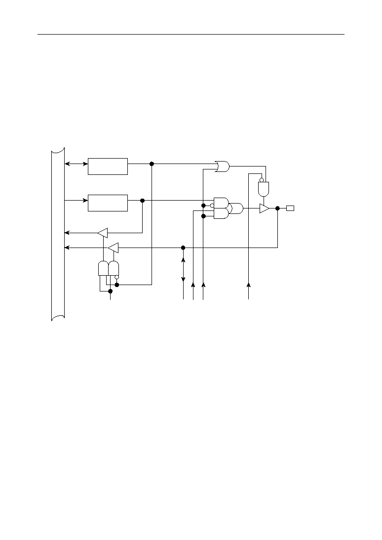
6-4
MSM66591/ML66592 User's Manual
Chapter 6 Port Functions
6.1.1 Configuration of Type A (P0_0≠P0_7, P1_0≠P1_7, P12_0)
Type A ports automatically take their secondary function when the
EA
pin is set to "L"
level. They function as address output pins and data I/O pins for external program
memory access. The pin specified as the output goes into high impedance if
OE
is in
"H" level.
In the ML66592, P12_1, also, is a Type A port.
Figure 6-1 shows the configuration of a Type A port.
Figure 6-1 Configuration of Type A
D A C
PmIOn
Pm_n
Pmn in
OE pin
External Memory Control signals
D: data
A: address
C: secondary function control signals
Pm_n
m = 0, 1
n = 0≠7
Internal Bus
m = 12
n = 0

6-5
MSM66591/ML66592 User's Manual
Chapter 6 Port Functions
6
Figure 6-2 Configuration of Type B
6.1.2 Configuration of Type B (P2_0≠P2_7, P3_0≠P3_3, P7_4≠P7_7, P8_0≠P8_7,
P10_0≠P10_4)
Some of the type B ports function as high-order address output when the external data
memory is accessed and the other ports act as secondary function input and output
pins, according to the specification of the secondary function control register (PmSFn).
The pin specified as the output goes into high impedance if
OE
is in "H" level.
Figure 6-2 shows the configuration of a Type B port.
C
PmIOn
OE pin
Secondary function control signals
C: secondary function control signal
O: secondary function output data
Pm_n
m = 2
n = 0≠7
m = 3
n = 0≠3
m = 7
n = 4≠7
m = 8
n = 0≠7
m = 10
n = 0≠4
Internal Bus
Pm_n
Read
Control
Out
Control
PmSFn
O
Pmn in
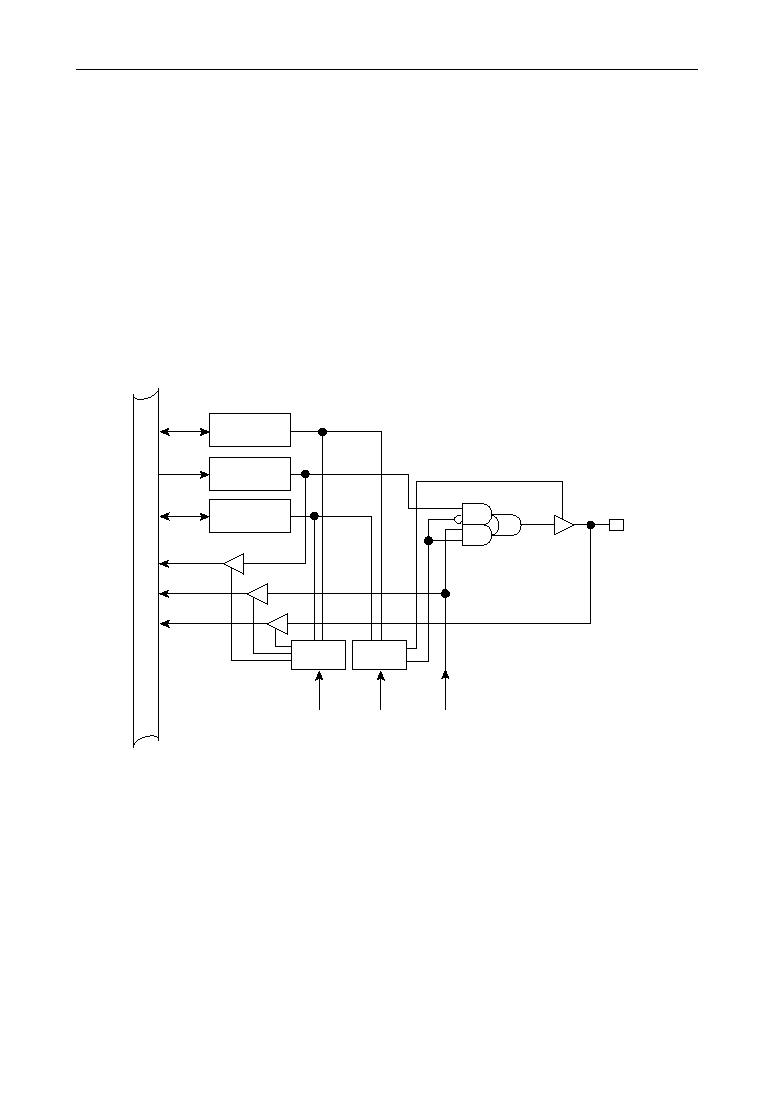
6-6
MSM66591/ML66592 User's Manual
Chapter 6 Port Functions
6.1.3 Configuration of Type C
(P3_4≠P3_7, P4_0≠P4_7, P5_0≠P5_7, P6_0≠P6_7,
P7_2, P7_3, P9_0≠P9_7, P10_5≠P10_7, P11_0≠P11_3)
Type C ports function as the output pins of secondary functions, or as input pins of
secondary functions according to the specification of the secondary function control
register (PmSFn).
However, P7_2 and P7_3 automatically switch to their secondary function when the
EA
pin is set to "L" level. Then, when external program memory is accessed, P7_3 func-
tions as an output pin (
PSEN
pin) for a strobe signal to be output for a read operation,
and P7_2 functions as an output pin (ALE pin) for a strobe signal used to externally
latch the low-order 8 bits of addresses that are output from P0.
Figure 6-3 shows the configuration of a Type C port.
Figure 6-3 Configuration of Type C
C
PmIOn
Secondary function control signals
C: secondary function control signal
I : secondary function input data
O: secondary function output data
Pm_n
m = 3
n = 4≠7
m = 4, 5, 6, 9
n = 0≠7
m = 7
n = 2, 3
m = 10
n = 5≠7
m = 11
n = 0≠3
Internal Bus
Pm_n
Read
Control
Out
Control
PmSFn
I or O
Pmn in
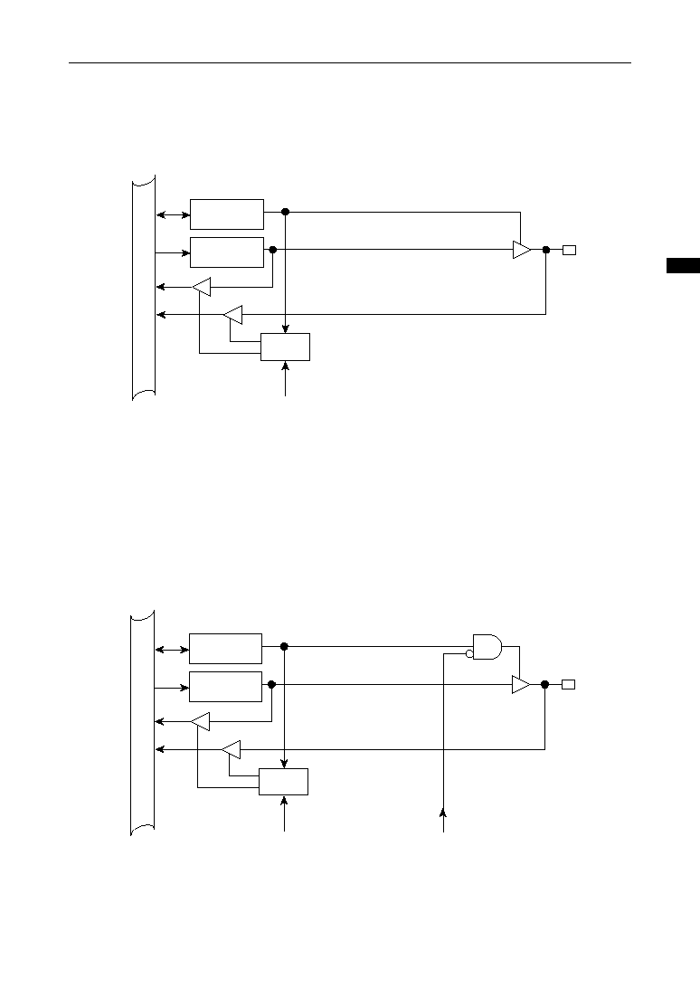
6-7
MSM66591/ML66592 User's Manual
Chapter 6 Port Functions
6
Figure 6-4 Configuration of Type D
6.1.4 Configuration of Type D (P7_0, P7_1, P11_4≠P11_7)
Type D ports function as I/O pins without secondary functions.
Figure 6-4 shows the configuration of Type D ports.
Figure 6-5 Configuration of Type E
6.1.5 Configuration of Type E (P12_1)
Type E ports function as I/O pins without secondary functions. When the
OE
pin is in "H"
level, the pin specified as the output goes into high impedance.
The ML66592 has no Type E ports.
Figure 6-5 shows the configuration of Type E port.
Pm_n
m = 7
n = 0, 1
m = 11
n = 4≠7
Internal Bus
PmIOn
Read
Control
Pm_n
Pmn in
Pm_n
m = 12
n = 1
Internal Bus
PmIOn
Read
Control
Pm_n
Pmn in
OE pin

6-8
MSM66591/ML66592 User's Manual
Chapter 6 Port Functions
6.2
Port Control Registers
The MSM66591/ML66592 have 3 types of port control registers.
∑ port data register (Pn: n = 0≠12)
∑ port mode register (PnIO: n = 0≠12)
∑ port secondary function control register (PnSF: n = 2≠10)
These registers are allocated as SFRs. Table 6-2 lists the port control registers.
6.2.1 Port Data Register (Pn: n = 0≠12)
A port data register (Pn: n = 0≠12) is an 8-bit register that stores the output data of a
port. Port 12, however, is a 2-bit register.
Pn is assigned to SFR, and the content of P0≠P12 becomes 00H at reset (when the
RES
signal is input, the BRK instruction is executed, the watchdog timer (WDT) is
overflown, or an operation code trap is generated).
If a read instruction is executed to Pn, the pin status ("0" or "1") is read from the port
specified to input, and the Pn status ("0" or "1") is read from the port specified to output.
If a write instruction is executed to Pn, data is written to Pn, regardless of the I/O
specification of the port.
Each of the bits assigned in a port is represented by the bit symbol corresponding to
each bit. Bit symbols for bits of a port data register are, for example, P0_0 for bit 0 and
P0_1 for bit 1 in Port 0. So, a port data register is represented correspending to each bit
either by the bit symbol such as P0_0 or P0_1 or by the dot operator such as P0.0 or
P0.1 in assembly language.
6.2.2 Port Mode Register (PnIO: n = 0≠12)
A port mode register (PnIO: n = 0≠12) is an 8-bit register that specifies the input/output
of an I/O port. Port 12, however, is a 2-bit register.
PnIO is assigned to SFR, and the content of P0IO≠P12IO becomes 00H. All ports
become input mode at reset (when the
RES
signal is input, the BRK instruction is
executed, the watchdog timer is overflown, or an operation code trap is generated).
If each bit of PnIO is set to "0", the input mode is set. If set to "1", the output mode is
set. However, as explained below, if the secondary function is selected after setting the
content of the port secondary function control register (PnSF: n = 2≠10) to "1", specifi-
cation by PnIO becomes invalid.
6.2.3 Port Secondary Function Control Register (PnSF: n = 2≠10)
A port secondary function control register (PnSF: n = 2≠10) is an 8-bit register that
specifies the primary/secondary functions of a port. Port 7 is a 6-bit register.

6-9
MSM66591/ML66592 User's Manual
Chapter 6 Port Functions
6
PnSF is assigned to SFR, and the content of P2SF≠P10SF becomes 00H, and all ports
are set to primary functions at reset (when the
RES
signal is input, the BRK instruction
is executed, the watchdog timer is overflown, or an operation code trap is generated).
If each bit of PnSF is set to "0", primary function is selected, and if "1", secondary
function is selected. Ports 0, 1, and 12 have no secondary function control register,
since the primary/secondary function of these ports is automatically selected by hard-
ware.
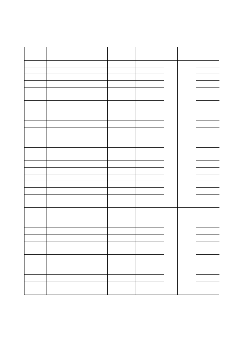
6-10
MSM66591/ML66592 User's Manual
Chapter 6 Port Functions
Table 6-2 Port Control SFRs
0015
001D
0021
0110
0111
Port 0 Data Register
0010
P0
00
Port 1 Data Register
0011
P1
00
Port 2 Data Register
0012
P2
00
Port 3 Data Register
0013
P3
00
Port 4 Data Register
0014
P4
00
Port 5 Data Register
P5
00
Port 6 Data Register
0016
P6
00
Port 7 Data Register
0017
P7
00
Port 8 Data Register
0018
P8
00
Port 9 Data Register
0019
P9
00
Port 10 Data Register
001A
P10
00
Port 11 Data Register
001B
P11
00
Port 2 Secondary Function Control Register
001C
P2SF
00
Port 3 Secondary Function Control Register
P3SF
00
Port 4 Secondary Function Control Register
001E
P4SF
00
Port 5 Secondary Function Control Register
001F
P5SF
00
Port 6 Secondary Function Control Register
0020
P6SF
00
Port 7 Secondary Function Control Register
P7SF
00
Port 8 Secondary Function Control Register
0022
P8SF
00
Port 9 Secondary Function Control Register
0023
P9SF
00
Port 10 Secondary Function Control Register
0024
P10SF
00
Port 12 Data Register
0025
P12
00
Port 0 Mode Register
P0IO
00
Port 1 Mode Register
P1IO
00
Port 2 Mode Register
0112
P2IO
00
Port 3 Mode Register
0113
P3IO
00
Port 4 Mode Register
0114
P4IO
00
Port 5 Mode Register
0115
P5IO
00
Port 6 Mode Register
0116
P6IO
00
Port 7 Mode Register
0117
P7IO
00
Port 8 Mode Register
0118
P8IO
00
Port 9 Mode Register
0119
P9IO
00
8
8
R/W
Port 10 Mode Register
011A
P10IO
00
Port 11 Mode Register
011B
P11IO
00
--
--
--
--
--
--
--
--
--
--
Port 12 Mode Register
011C
P12IO
00
--
--
--
--
--
--
--
--
--
--
--
--
--
--
--
--
--
--
--
--
--
--
--
--
--
8
R/W
8
R/W
R/W
Some addresses are not consecutive.
Addresses in the address column marked by "" indicate that the register has bits missing.
Address [H]
Name
Abbreviated
Name (BYTE)
R/W
8/16-Bit
Operation
Reset
State [H]
Abbreviated
Name (WORD)

6-11
MSM66591/ML66592 User's Manual
Chapter 6 Port Functions
6
Figure 6-6 Configuration of P0, P0IO
If a read instruction is executed to a P0 in which input is specified (P0IOn = "0") by
P0IO, the content of the pin is read; and if a read instruction is executed to a P0 in
which output is specified (P0IOn = "1"), the content of the port data register is read.
If an arithmetic instruction, increment instruction, or instruction of that type (read-
modify-write instruction) is executed to P0, the content of the pin or port data register is
read according to specification by P0IO (in the case of reading), and data is written to
the port data register (in the case of writing).
At reset (when the
RES
signal is input, the BRK instruction is executed, the watchdog
timer is overflown, or an operation code trap is generated), Port 0 goes into high
impedance input port (P0IO = 00H). The content of P0 becomes 00H.
P0_7
P0_6
P0_5
P0_4
P0_3
P0_2
P0_1
P0_0
7
6
5
4
3
2
1
0
P0
P0IO7
P0IO6
P0IO5
P0IO4
P0IO3
P0IO2
P0IO1
P0IO0
7
6
5
4
3
2
1
0
P0IO
P0_n = input
0
P0_n = output
1
n = 0≠7
6.3
Port 0 (P0)
Port 0 (P0_0≠P0_7) is an 8-bit I/O port. Input or output can be specified for each bit by
the Port 0 mode register (P0IO).
In addition to its port function, Port 0 is assigned a secondary function (low-order
address output and data input of external program memory). If the
EA
pin is set to "L"
level, Port 0 automatically operates as its secondary function, as an address/data bus
(low-order address output pin, data I/O pin).
If the
OE
pin (pin 71) is in "L" level when Port 0 is in output status, Port 0 outputs "H" or
"L" level, but if the
OE
pin is in "H" level, Port 0 goes into high impedance status.
Figure 6-6 shows the configuration of the Port 0 data register (P0) and the Port 0 mode
register (P0IO).
6-12
MSM66591/ML66592 User's Manual
Chapter 6 Port Functions
6.4
Port 1 (P1)
Port 1 (P1_0≠P1_7) is an 8-bit I/O port. Input or output can be specified for each bit by
the Port 1 mode register (P1IO).
In addition to the port function, a secondary function (high address output of external
program memory) is assigned to Port 1. If the
EA
pin is set to "L" level, Port 1 operates as
an address bus (high address output pin) of the external program memory.
If the
OE
pin (pin 71) is in "L" level when Port 1 is in output status, Port 1 outputs "H" or
"L" level, but if the
OE
pin is in "H" level, Port 1 goes into high impedance status.
Figure 6-7 shows the configuration of the Port 1 data register (P1) and the Port 1 mode
register (P1IO).
Figure 6-7 Configuration of P1, P1IO
If a read instruction is executed to P1 in which input is specified (P1IOn = "0") by P1IO,
the content of the pin is read. If a read instruction is executed to P1 in which output is
specified (P1IOn = "0"), the content of the port data register is read. If an arithmetic
instruction, increment instruction, or instruction of that type (read-modify-write instruc-
tion) is executed to P1, the content of the pin or port data register is read according to
specification by P1IO (in the case of reading), and data is written to the port data register
(in the case of writing).
At reset (when the
RES
signal is input, the BRK instruction is executed, the watchdog
timer is overflown, or an operation code trap is generated), Port 1 becomes a high
impedance input port (P1IO = 00H). The content of P1 becomes 00H.
P1_7
P1_6
P1_5
P1_4
P1_3
P1_2
P1_1
P1_0
7
6
5
4
3
2
1
0
P1
P1IO7
P1IO6
P1IO5
P1IO4
P1IO3
P1IO2
P1IO1
P1IO0
7
6
5
4
3
2
1
0
P1IO
P1_n = input
0
P1_n = output
1
n = 0≠7

6-13
MSM66591/ML66592 User's Manual
Chapter 6 Port Functions
6
6.5
Port 2 (P2)
Port 2 (P2_0≠P2_7) is an 8-bit I/O port. Input or output can be specified for each bit by
the Port 2 mode register (P2IO).
In addition to the port function, a secondary function (real-time output, etc.) is assigned
to Port 2. Port function/secondary function is selected by the Port 2 secondary function
control register (P2SF).
If the
OE
pin (pin 71) is in "L" level when Port 2 is in output status, Port 2 outputs "H" or
"L" level, but if the
OE
pin is in "H" level, Port 2 goes into high impedance status.
Figure 6-8 shows the configuration of the Port 2 data register (P2), the Port 2 mode
register (P2IO), and the Port 2 secondary function control register (P2SF).
P2_7
P2_6
P2_5
P2_4
P2_3
P2_2
P2_1
P2_0
7
6
5
4
3
2
1
0
P2
P2IO7
P2IO6
P2IO5
P2IO4
P2IO3
P2IO2
P2IO1
P2IO0
7
6
5
4
3
2
1
0
P2IO
P2_n = input
0
P2_n = output
1
n = 0≠7
RTO11 RTO10
RTO9
RTO8
RTO7
RTO6
RTO5
RTO4
7
6
5
4
3
2
1
0
P2SF
P2_0
0
Flexible timer realtime output 4
1
P2_1
0
Flexible timer realtime output 5
1
P2_2
0
Flexible timer realtime output 6
1
P2_3
0
Flexible timer realtime output 7
1
P2_4
0
Flexible timer realtime output 8
1
P2_5
0
Flexible timer realtime output 9
1
P2_6
0
Flexible timer realtime output 10
1
P2_7
0
Flexible timer realtime output 11
1
Figure 6-8 Configuration of P2, P2IO, and P2SF
6-14
MSM66591/ML66592 User's Manual
Chapter 6 Port Functions
Table 6-3 shows the content of the data that is read when a read instruction is executed
to P2, according to the content of P2IO and P2SF. If an arithmetic instruction, incre-
ment instruction, or instruction of that type (read-modify-write instruction) is executed to
P2, the content of the pin or port data register is read according to specification by P2IO
(when reading), and data is written to the port data register (when writing).
At reset (when the
RES
signal is input, the BRK instruction is executed, the watchdog
timer is overflown, or an operation code trap is generated), Port 2 becomes a high
impedance input port (P2IO = 00H, P2SF = 00H). The content of P2 becomes 00H.
Table 6-3 Read of P2
P2_0≠P2_7
P2IO
P2SF
Read Data
0
0
Pin
1
0
Output latch
*
1
Output data
"*" indicates either "1" or "0".
6-15
MSM66591/ML66592 User's Manual
Chapter 6 Port Functions
6
6.6
Port 3 (P3)
Port 3 (P3_0≠P3_7) is an 8-bit I/O port. Input or output can be specified for each bit by
the Port 3 mode register (P3IO).
In addition to the port function, a secondary function (real-time output, etc.) is assigned
to Port 3. Port function/secondary function is selected by the Port 3 secondary function
control register (P3SF).
Figure 6-9 shows the configuration of the Port 3 data register (P3), the Port 3 mode
register (P3IO), and the Port 3 secondary function control register (P3SF).
Figure 6-9 Configuration of P3, P3IO, and P3SF
P3_7
P3_6
P3_5
P3_4
P3_3
P3_2
P3_1
P3_0
7
6
5
4
3
2
1
0
P3
P3IO7
P3IO6
P3IO5
P3IO4
P3IO3
P3IO2
P3IO1
P3IO0
7
6
5
4
3
2
1
0
P3IO
P3_n = input
0
P3_n = output
1
n = 0≠7
CAP3
CAP2
CAP1
CAP0
FTM17D FTM17C FTM17B FTM17A
7
6
5
4
3
2
1
0
P3SF
P3_0
0
Flexible timer I/O 17A
1
P3_1
0
Flexible timer realtime output 17B
1
P3_2
0
Flexible timer realtime output 17C
1
P3_3
0
Flexible timer realtime output 17D
1
P3_4
0
Flexible timer capture input 0
1
P3_5
0
Flexible timer capture input 1
1
P3_6
0
Flexible timer capture input 2
1
P3_7
0
Flexible timer capture input 3
1

6-16
MSM66591/ML66592 User's Manual
Chapter 6 Port Functions
Table 6-4 shows the content of the data that is read when a read instruction is executed
to P3 according to the content of P3IO and P3SF. If an arithmetic instruction, increment
instruction, or instruction of that type (read-modify-write instruction) is executed to P3,
the content of the pin or port data register is read according to specification by P3IO
(when reading), and data is written to the port data register (when writing).
At reset (when the
RES
signal is input, the BRK instruction is executed, the watchdog
timer is overflown, or an operation code trap is generated), Port 3 becomes a high
impedance input port (P3IO, P3SF = 00H). The content of P3 becomes 00H.
Table 6-4 Read of P3
P3_0
P3_1≠P3_3
P3IO
P3SF
Read Data
0
0
Pin
1
0
Output latch
*
Pin: if timer is in CAP mode
Output data: if timer is in RTO mode
0
0
Pin
1
0
Output latch
1
Output data
0
0
Pin
1
0
Output latch
P3_4≠P3_7
Pin
1
*
"*" indicates either "1" or "0".
*
1

6-17
MSM66591/ML66592 User's Manual
Chapter 6 Port Functions
6
6.7
Port 4 (P4)
Port 4 (P4_0≠P4_7) is an 8-bit I/O port. Input or output can be specified for each bit by
the Port 4 mode register (P4IO).
In addition to the port function, a secondary function (transition detector input) is
assigned to Port 4. Port function/secondary function is selected by the Port 4 secondary
function control register (P4SF).
Figure 6-10 shows the configuration of the Port 4 data register (P4), the Port 4 mode
register (P4IO), and the Port 4 secondary function control register (P4SF).
Figure 6-10 Configuration of P4, P4IO, and P4SF
P4_7
P4_6
P4_5
P4_4
P4_3
P4_2
P4_1
P4_0
7
6
5
4
3
2
1
0
P4
P4IO7
P4IO6
P4IO5
P4IO4
P4IO3
P4IO2
P4IO1
P4IO0
7
6
5
4
3
2
1
0
P4IO
P4_n = input
0
P4_n = output
1
n = 0≠7
TRNS7 TRNS6 TRNS5 TRNS4 TRNS3 TRNS2 TRNS1 TRNS0
7
6
5
4
3
2
1
0
P4SF
P4_0
0
Transition detector 0 input
1
P4_1
0
Transition detector 1 input
1
P4_2
0
Transition detector 2 input
1
P4_3
0
Transition detector 3 input
1
P4_4
0
Transition detector 4 input
1
P4_5
0
Transition detector 5 input
1
P4_6
0
Transition detector 6 input
1
P4_7
0
Transition detector 7 input
1
6-18
MSM66591/ML66592 User's Manual
Chapter 6 Port Functions
Table 6-5 shows the content of the data that is read when a read instruction is executed
to P4 according to the content of P4IO and P4SF. If an arithmetic instruction, increment
instruction, or instruction of that type (read-modify-write instruction) is executed to Port
4, the content of the pin or port data register is read according to specification by P4IO
(when reading), and data is written to the port data register (when writing).
At reset (when the
RES
signal is input, the BRK instruction is executed, the watchdog
timer is overflown, or an operation code trap is generated), Port 4 becomes a high
impedance input port (P4IO, P4SF = 00H). The content of P4 becomes 00H.
Table 6-5 Read of P4
P4_0≠P4_7
P4IO
P4SF
Read Data
0
0
Pin
1
0
Output latch
*
1
Pin
"*" indicates either "1" or "0".
6-19
MSM66591/ML66592 User's Manual
Chapter 6 Port Functions
6
P5SF
7
6
5
4
3
2
1
0
WAIT CLKOUT INT2
CSB
RWB
SCLK SDOUT SDIN
0
P5_0
1
Data input for SCI5 with FIFO
0
P5_1
1
Data output for SCI5 with FIFO
0
P5_2
1
Clock output for SCI5 with FIFO
0
P5_3
1
R/WB output for SCI5 with FIFO
0
P5_4
1
Chip select output for SCI5 with FIFO
0
P5_5
1
External interrupt 2 input
0
P5_6
1
Dividing clock output
0
P5_7
1
WAIT input for SCI5 with FIFO
P5_7
P5_6
P5_5
P5_4
P5_3
P5_2
P5_1
P5_0
7
6
5
4
3
2
1
0
P5
P5IO7
P5IO6
P5IO5
P5IO4
P5IO3
P5IO2
P5IO1
P5IO0
7
6
5
4
3
2
1
0
P5IO
P5_n = input
0
P5_n = output
1
n = 0≠7
6.8
Port 5 (P5)
Port 5 (P5_0≠P5_7) is a 8-bit I/O port. Input or output can be specified for each bit by
the Port 5 mode register (P5IO).
In addition to the port function, a secondary function (serial interface with FIFO) is
assigned to Port 5. Port function/secondary function is selected by the Port 5 secondary
function control register (P5SF).
Figure 6-11 shows the configuration of the Port 5 data register (P5), Port 5 mode
register (P5IO), and Port 5 secondary function control register (P5SF).
Figure 6-11 Configuration of P5, P5IO, and P5SF

6-20
MSM66591/ML66592 User's Manual
Chapter 6 Port Functions
If a read instruction is executed to P5 in which the input is specified (P5IOn = "0")
by P5IO, the content of the pin is read. If a read instruction is executed to P5 in which
the output is specified (P5IOn = "1"), the content of the port data register is read.
If an arithmetic instruction, increment instruction, or instruction of that type (read-
modify-write instruction) is executed to P5, the content of the pin or port data register is
read according to specification by P5IO (when reading), and data is written to the port
data register (when writing).
At reset (when the
RES
signal is input, the BRK instruction is executed, the watchdog
timer is overflown, or an operation code trap is generated), Port 5 becomes high
impedance input port (P5IO = 00H, P5SF = 00H). The content of P5 becomes 00H.
6-21
MSM66591/ML66592 User's Manual
Chapter 6 Port Functions
6
6.9
Port 6 (P6)
Port 6 (P6_0≠P6_7) is an 8-bit I/O port. Input or output can be specified for each bit by
the Port 6 mode register (P6IO).
In addition to the port function, a secondary function (external interrupt input, etc.) is
assigned to Port 6. Port function/secondary function is selected by the Port 6 secondary
function control register (P6SF).
Figure 6-12 shows the configuration of the Port 6 data register (P6), the Port 6 mode
register (P6IO), and the Port 6 secondary function control register (P6SF).
Figure 6-12 Configuration of P6, P6IO, and P6SF
P6_7
P6_6
P6_5
P6_4
P6_3
P6_2
P6_1
P6_0
7
6
5
4
3
2
1
0
P6
P6IO7
P6IO6
P6IO5
P6IO4
P6IO3
P6IO2
P6IO1 P6IO0
7
6
5
4
3
2
1
0
P6IO
P6_n = input
0
P6_n = output
1
n = 0≠7
TXD0
RXD0
TXC1
RXC1
TXD1
RXD1
INT1
INT0
7
6
5
4
3
2
1
0
P6SF
P6_0
0
External interrupt 0 input
1
P6_1
0
External interrupt 1 input
1
P6_2
0
Serial port 1 receive data input
1
P6_3
0
Serial port 1 transmit data output
1
P6_4
0
Shift clock I/O for serial port 1 receive
1
P6_5
0
Shift clock I/O for serial port 1 transmit
1
P6_6
0
Serial port 0 receive data input
1
P6_7
0
Serial port 0 transmit data output
1
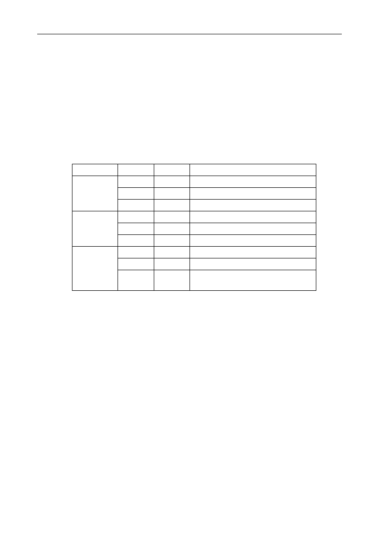
6-22
MSM66591/ML66592 User's Manual
Chapter 6 Port Functions
P6_0≠P6_2,
P6_6
P6_3, P6_7
P6IO
P6SF
Read Data
0
0
Pin
1
0
Output latch
*
1
Pin
0
0
Pin
*
0
Output latch
1
1
Output data latch
0
0
Pin
1
0
Output latch
*
Clock: if shift clock is output
Pin: if shift clock is input
P6_4, P6_5
"*" indicates either "1" or "0".
1
Table 6-6 shows the content of the data that is read when a read instruction is executed
to P6 according to the content of P6I0 and P6SF. If an arithmetic instruction, increment
instruction, or instruction of that type (read-modify-write instruction) is executed to Port
6, the content of the pin or port data register is read according to specification by P6IO
(when reading), and data is written to the port data register (when writing).
At reset (when the
RES
signal is input, the BRK instruction is executed, the watchdog
timer is overflown, or an operation code trap is generated), Port 6 becomes a high
impedance input port (P6IO, P6SF = 00H). The content of P6 becomes 00H.
Table 6-6 Read of P6
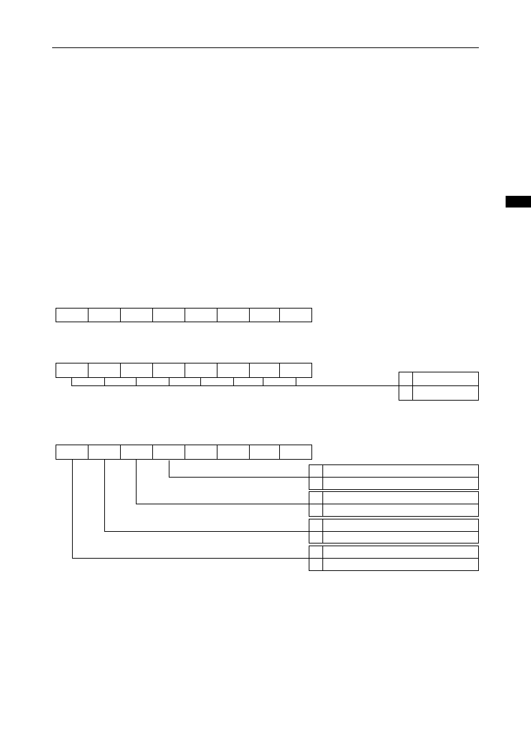
6-23
MSM66591/ML66592 User's Manual
Chapter 6 Port Functions
6
Figure 6-13 Configuration of P7, P7IO, and P7SF
P7_7
P7_6
P7_5
P7_4
P7_3
P7_2
P7_1
P7_0
7
6
5
4
3
2
1
0
P7
P7IO7
P7IO6
P7IO5
P7IO4
P7IO3
P7IO2 P7IO1 P7IO0
7
6
5
4
3
2
1
0
P7IO
P7_n = input
0
P7_n = output
1
n = 0≠7
PWM3 PWM2 PWM1 PWM0
"0"
"0"
"0"
"0"
7
6
5
4
3
2
1
0
P7SF
P7_4
0
PWM0 output
1
P7_5
0
PWM1 output
1
P7_6
0
PWM2 output
1
P7_7
0
PWM3 output
1
"0" indicates a bit that is not provided.
"0" is read if a read instruction
is executed.
When writing to these bits,
always write "0".
6.10 Port 7 (P7)
Port 7 (P7_0≠P7_7) is an 8-bit I/O port. Input or output can be specified for each bit by
the Port 7 mode register (P7IO). In addition to the port function, a secondary function
(output of the strobe signal for the external memory, etc) is assigned to Port 7. Port
function/secondary function is selected by the Port 7 secondary function control register
(P7SF).
When the
EA
pin is set to "L" level, P7_2 and P7_3 automatically operates as the
PSEN
pin and the ALE pin respectively.
If the
OE
pin (pin 71) is in "L" level when P7_4≠P7_7 are in output status, P7_4≠P7_7
output in "H" or "L" level. But if the
OE
pin is in "H" level, P7_4≠P7_7 go into high
impedance.
Figure 6-13 shows the configuration of the Port 7 data register (P7), the Port 7 mode
register (P7IO), and the Port 7 secondary function control register (P7SF).

6-24
MSM66591/ML66592 User's Manual
Chapter 6 Port Functions
Table 6-7 shows the content of the data that is read when a read instruction is executed
to P7 according to the content of P7IO and P7SF. If an arithmetic instruction, increment
instruction, or instruction of that type (read-modify-write instruction) is executed to P7,
the content of the pin or port data register is read according to specification by P7IO
(when reading), and data is written to the port data register (when writing).
At reset (when the
RES
signal is input, the BRK instruction is executed, the watchdog
timer is overflown, or an operation code trap is generated), Port 7 becomes a high
impedance input port (P7IO, P7SF = 00H). The content of P7 becomes 00H.
Table 6-7 Read of P7
P7_0≠P7_3
P7_4≠P7_7
P7IO
P7SF
Read Data
0
--
Pin
1
--
Output latch
0
0
Pin
*
0
Output latch
1
1
Output data
"--" indicates a bit that is not provided and "*" indicates either "1" or "0".
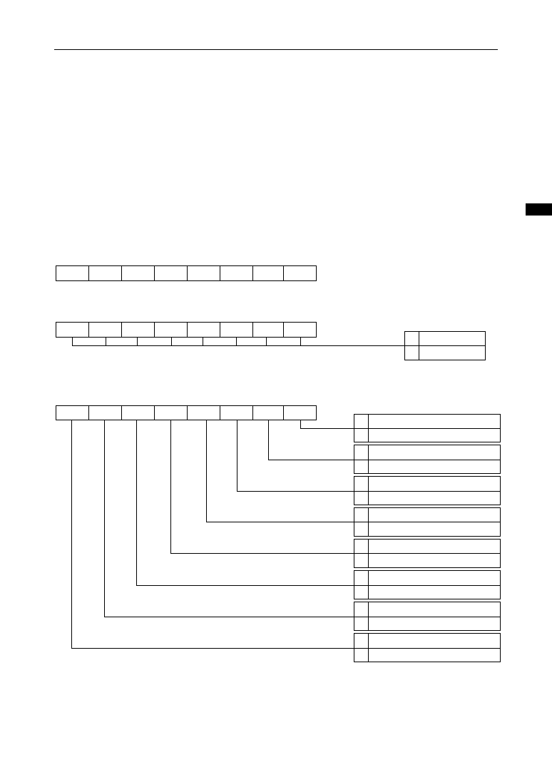
6-25
MSM66591/ML66592 User's Manual
Chapter 6 Port Functions
6
6.11 Port 8 (P8)
Port 8 (P8_0≠P8_7) is an 8-bit I/O port. Input or output can be specified for each bit by
the Port 8 mode register (P8IO). In addition to the port function, a secondary function
(PWM output) is assigned to Port 8. Port function/secondary function is selected by the
Port 8 secondary function control register (P8SF).
If the
OE
pin (pin 71) is in "L" level when Port 8 is in output status, Port 8 outputs "H" or
"L" level. But if the
OE
pin (pin 71) is in "H" level, Port 8 goes into high impedance
status.
Figure 6-14 shows the configuration of the Port 8 data register (P8), the Port 8 mode
register (P8IO), and the Port 8 secondary function control register (P8SF).
Figure 6-14 Configuration of P8, P8IO, and P8SF
P8_7
P8_6
P8_5
P8_4
P8_3
P8_2
P8_1
P8_0
7
6
5
4
3
2
1
0
P8
P8IO7
P8IO6
P8IO5
P8IO4
P8IO3
P8IO2 P8IO1 P8IO0
7
6
5
4
3
2
1
0
P8IO
P8_n = input
0
P8_n = output
1
n = 0≠7
PWM11 PWM10 PWM9 PWM8 PWM7 PWM6 PWM5 PWM4
7
6
5
4
3
2
1
0
P8SF
0
P8_0
1
PWM4 output
0
P8_1
1
PWM5 output
0
P8_2
1
PWM6 output
0
P8_3
1
PWM7 output
0
P8_4
1
PWM8 output
0
P8_5
1
PWM9 output
0
P8_6
1
PWM10 output
0
P8_7
1
PWM11 output

6-26
MSM66591/ML66592 User's Manual
Chapter 6 Port Functions
Table 6-8 shows the content of the data that is read when a read instruction is executed
to P8 according to the content of P8I0 and P8SF. If an arithmetic instruction, increment
instruction, or instruction of that type (read-modify-write instruction) is executed to P8,
the content of the pin or port data register is read according to specification by P8IO
when reading, and data is written to the port data register when writing.
At reset (when the
RES
signal is input, the BRK instruction is executed, the watchdog
timer is overflown, or an operation code trap is generated), Port 8 becomes a high
impedance input port (P8IO = 00H, P8SF = 00H). The content of P8 becomes 00H.
Table 6-8 Read of P8
P8_0≠P8_7
P8IO
P8SF
Read Data
0
0
Pin
1
0
Output latch
*
1
Output data
"*" indicates either "1" or "0".
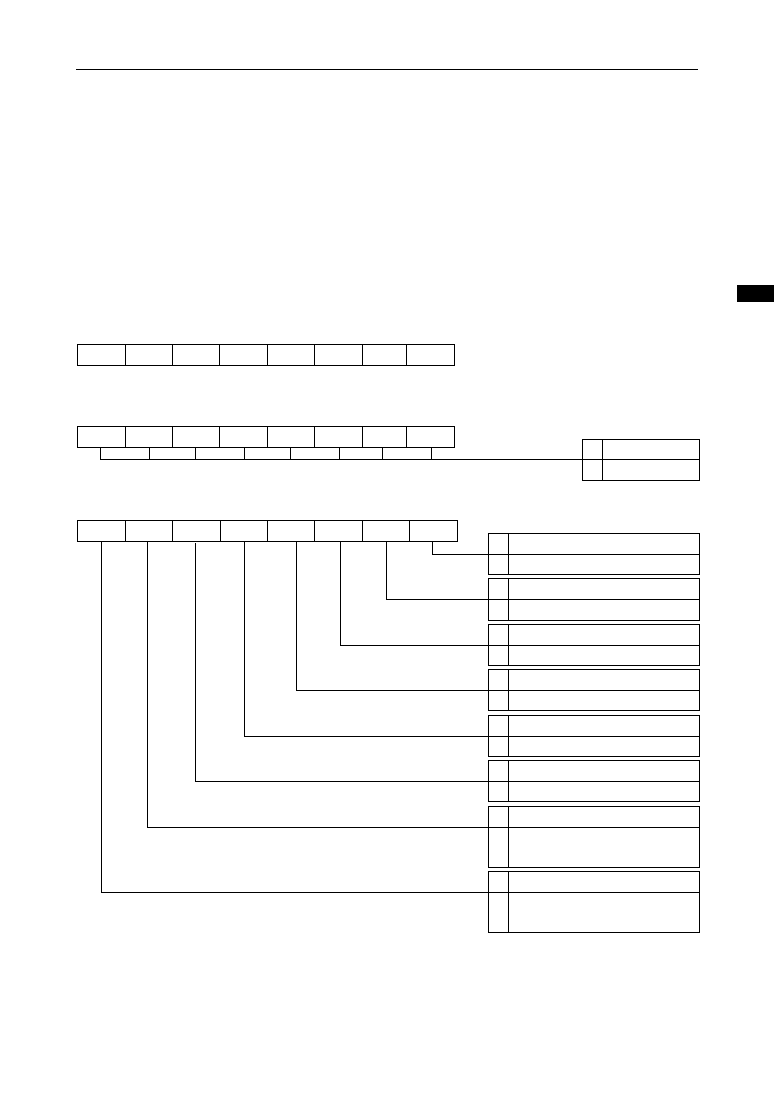
6-27
MSM66591/ML66592 User's Manual
Chapter 6 Port Functions
6
6.12 Port 9 (P9)
Port 9 (P9_0 ≠ P9_7) is an 8-bit I/O port. Input or output can be specified for each bit by
the Port 9 mode register (P9IO).
In addition to the port function, a secondary function (serial port I/O, etc) is assigned to
Port 9. Port function/secondary function is selected by the Port 9 secondary function
control register (P9SF).
Figure 6-15 shows the configuration of the Port 9 data register (P9), the Port 9 mode
register (P9IO), and the Port 9 secondary function control register (P9SF).
Figure 6-15 Configuration of P9, P9IO, and P9SF
P9_7
P9_6
P9_5
P9_4
P9_3
P9_2
P9_1
P9_0
7
6
5
4
3
2
1
0
P9
P9IO7
P9IO6
P9IO5
P9IO4
P9IO3
P9IO2 P9IO1 P9IO0
7
6
5
4
3
2
1
0
P9IO
P9_n = input
0
P9_n = output
1
n = 0≠7
P9SF
7
6
5
4
3
2
1
0
ECTCK ETMCK TXD4
RXD4
TXD3
RXD3
TXD2
RXD2
0
P9_0
1
Serial port 2 receive data input
0
P9_1
1
Serial port 2 transmit data output
0
P9_2
1
Serial port 3 receive data input
0
P9_3
1
Serial port 3 transmit data output
0
P9_4
1
Serial port 4 receive data input
0
P9_5
1
Serial port 4 transmit data output
0
P9_6
1
External clock input for general
-purpose 8-bit timer
0
P9_7
1
External clock input for general
-purpose 8-bit event counter

6-28
MSM66591/ML66592 User's Manual
Chapter 6 Port Functions
If a read instruction is executed to P9 in which the input is specified (P9IOn = "0")
by P9IO, the content of the pin is read. If a read instruction is executed to P9 in which
the output is specified (P9IOn = "1"), the content of the port data register is read.
If an arithmetic instruction, increment instruction, or instruction of that type (read-
modify-write instruction) is executed to P9, the content of the pin or port data register is
read according to specification by P9IO (when reading), and data is written to the port
data register (when writing).
At reset (when the
RES
signal is input, the BRK instruction is executed, the watchdog
timer is overflown, or an operation code trap is generated), Port 9 becomes a high
impedance input port (P9IO, P9SF = 00H). The content of P9 becomes 00H.
6-29
MSM66591/ML66592 User's Manual
Chapter 6 Port Functions
6
6.13 Port 10 (P10)
Port 10 (P10_0≠P10_7) is an 8-bit I/O port. Input or output can be specified for each bit
by the Port 10 mode register (P10IO). In addition to the port function, a secondary
function (real time output, etc) is assigned to Port 10. Port function/secondary function
is selected by the Port 10 secondary function control register (P10SF).
If the
OE
pin (pin 71) is in "L level when P10_0≠P10_4 are in output status, Port 10
outputs "H" or "L" level. But if the
OE
pin (pin 71) is in "H" level, Port 10 goes into high
impedance status.
Figure 6-16 shows the configuration of the Port 10 data register (P10), the Port 10
mode register (P10IO), and the Port 10 secondary function control register (P10SF).
Figure 6-16 Configuration of P10, P10IO, and P10SF
P10_7
P10_6
P10_5
P10_4
P10_3
P10_2
P10_1 P10_0
7
6
5
4
3
2
1
0
P10
P10IO7 P10IO6 P10IO5 P10IO4 P10IO3 P10IO2 P10IO1 P10IO0
7
6
5
4
3
2
1
0
P10IO
P10_n = input
0
P10_n = output
1
n = 0≠7
P10SF
7
6
5
4
3
2
1
0
SFTSTB SFTDAT
SFTCLK FTM16 CAP15 CAP14 RTO13 RTO12
0
P10_0
1
RTO12 output
0
P10_1
1
RTO13 output
0
P10_2
1
Flexible timer capture input 14
0
P10_3
1
Flexible timer capture input 15
0
P10_4
1
Flexible timer I/O 16
0
P10_5
1
Expansion port shift clock
0
P10_6
1
Expansion port data I/O
0
P10_7
1
Expansion port latch strobe output

6-30
MSM66591/ML66592 User's Manual
Chapter 6 Port Functions
Table 6-9 shows the content of the data that is read when a read instruction is executed
to P10 according to the content of P10I0 and P10SF. If an arithmetic instruction,
increment instruction, or instruction of that type (read-modify-write instruction) is ex-
ecuted to P10, the content of the pin or port data register is read according to specifica-
tion by P10IO (when reading), and data is written to the port data register (when
writing).
At reset (when the
RES
signal is input, the BRK instruction is executed, the watchdog
timer is overflown, or an operation code trap is generated), Port 10 becomes a high
impedance input port (P10IO, P10SF = 00H). The content of P10 becomes 00H.
Table 6-9 Read of P10
"*" indicates either "1" or "0".
P10_0, P10_1
P10_5, P10_7
P10_4
P10IO
1
*
0
P10SF
0
1
0
1
0
P10_6
Read Data
Pin
Output latch
Output data
Pin
Output latch
Pin: if timer is in CAP mode
Output data: if timer is in RTO mode
*
1
0
0
1
0
Pin
Output latch
0
0
P10_2, P10_3
1
*
0
1
Pin
Output latch
Pin
0
0
*
1
Pin: if expansion port is in input mode
Output data: if expansion port is in output mode

6-31
MSM66591/ML66592 User's Manual
Chapter 6 Port Functions
6
6.14 Port 11 (P11)
Port 11 (P11_0≠P11_7) is an 8-bit I/O port. Input or output can be specified for each bit
by the Port 11 mode register (P11IO).
In addition to the port function, a secondary function (RAM monitor function) is assigned
to port 11. The RAM monitor function is enabled when the
EA
pin is set to "H" level.
Figure 6-17 shows the configuration of the Port 11 data register (P11) and the Port 11
mode register (P11IO).
P11_7
P11_6
P11_5
P11_4
P11_3
P11_2
P11_1 P11_0
7
6
5
4
3
2
1
0
P11
P11IO7 P11IO6 P11IO5 P11IO4 P11IO3 P11IO2 P11IO1 P11IO0
7
6
5
4
3
2
1
0
P11IO
P11_n = input
0
P11_n = output
1
n = 0≠7
Figure 6-17 Configuration of P11 and P11IO
If a read instruction is executed to P11 in which the input is specified (P11IOn = "0")
by P11IO, the content of the pin is read. If a read instruction is executed to P11 in which
the output is specified (P11IOn = "1"), the content of the port data register is read.
If an arithmetic instruction, increment instruction, or instruction of that type (read-
modify-write instruction) is executed to P11, the content of the pin or port data register
is read according to specification by P11IO (when reading), and data is written to the
port data register (when writing).
At reset (when the
RES
signal is input, the BRK instruction is executed, the watchdog
timer is overflown, or an operation code trap is generated), Port 11 becomes a high
impedance input port (P11IO = 00H). The content of P11 becomes 00H.
6-32
MSM66591/ML66592 User's Manual
Chapter 6 Port Functions
6.15 Port 12 (P12)
Port 12 (P12_0, P12_1) is a 2-bit I/O port. Input or output can be specified for each bit
by the Port 12 mode register (P12IO).
In addition to the port function, a secondary function (for MSM66591, address 16 output
of external program memory; for ML66592, address 16 and 17 output of external
program memory) is assigned to Port 12. If the
EA
pin is set to "L" level, in MSM66591
P12_0 operates as an address bus (address 16 output pin) of the external program
memory, and in ML66592 P12_0 and P12_1 operate as address buses (address 16
and 17 output pins) of the external program memory.
If the
OE
pin (pin 71) is in "L" level when Port 12 is in output status, Port 12 outputs "H"
or "L" level, but if the
OE
pin is in "H" level, Port 12 goes into high impedance status.
Figure 6-18 shows the configuration of the Port 12 data register (P12) and the Port 12
mode register (P12IO).
Figure 6-18 Configuration of P12 and P12IO
If a read instruction is executed to P12 in which input is specified (P12IOn = "0") by
P12IO, the content of the pin is read. If a read instruction is executed to P12 in which
output is specified (P12IOn = "0"), the content of the port data register is read. If an
arithmetic instruction, increment instruction, or instruction of that type (read-modify-
write instruction) is executed to P12, the content of the pin or port data register is read
according to specification by P12IO (in the case of reading), and data is written to the
port data register (in the case of writing).
At reset (when the
RES
signal is input, the BRK instruction is executed, the watchdog
timer is overflown, or an operation code trap is generated), Port 12 becomes a high
impedance input port (P12IO = 00H). The content of P12 becomes 00H.
"0"
"0"
"0"
"0"
"0"
"0"
P12_1
P12_0
7
6
5
4
3
2
1
0
P12
"0"
"0"
"0"
"0"
"0"
"0"
P12IO1 P12IO0
7
6
5
4
3
2
1
0
P12IO
P12_n = input
0
P12_n = output
1
n = 0, 1
"0" indicates a bit that is not provided.
"0" is read if a read instruction
is executed.
When writing to these bits,
always write "0".

Output Pin Control Pin (OE)
Chapter 7
7

7-1
MSM66591/ML66592 User's Manual
Chapter 7 Output Pin Control Pin (OE)
7
7.
Output Pin Control Pin (
OE
)
The MSM66591/ML66592 have an
OE
pin (pin 71) to control the output of 47 pins, P0,
P1, P2, P3_0≠P3_3, P7_4≠P7_7, P8, P10_0≠P10_4, P12_0, and P12_1.
If the
OE
pin is in "H" level when P0, P1, P2, P3_0≠P3_3, P7_4≠P7_7, P8, P10_0≠
P10_4, P12_0, and P12_1 are configured to function as output pins, each pin goes into
high impedance status, and if the
OE
pin is in "L" level, each pin outputs "L" or "H" level.
When P0, P1, P2, P3_0≠P3_3, P7_4≠P7_7, P8, P10_0≠P10_4, P12_0, and P12_1 are
specified to input, each pin functions as an input pin, regardless of the status of the
OE
pin.
The level of the
OE
pin can be read by testing bit 7 (OERD) of the peripheral control
register (PRPHF) by the program.

7-2
MSM66591/ML66592 User's Manual
Chapter 7 Output Pin Control Pin (OE)

Clock Generation Circuit
Chapter 8
8

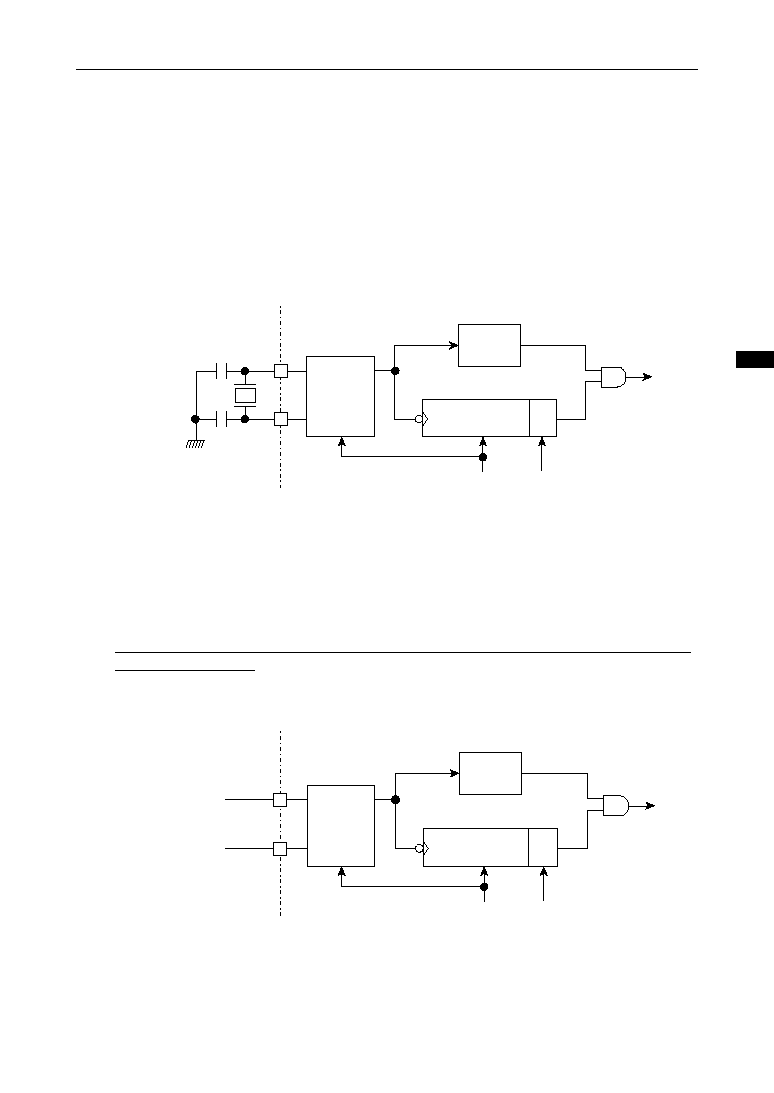
8-1
MSM66591/ML66592 User's Manual
Chapter 8 Clock Generation Circuit
8
8.
Clock Generation Circuit
The clock generation circuit generates the master clock pulse (CLK) necessary for the
MSM66591/ML66592. In other words, the clock generation circuit multiplies the clock
generated by the oscillation circuit by a factor of 2, then supplies the obtained clock to
the MSM66591/ML66592. A crystal oscillator or other required devices are connected
to OSC0 (pin 42) and OSC1 (pin 43) pins.
Figure 8-1 shows an example of a crystal oscillation circuit.
If the master clock pulse is supplied externally, input to the OSC0 pin. Leave the OSC1
pin open at that time.
Figure 8-2 shows the connection example for external clock input.
Figure 8-1 An Example of a Crystal Oscillation Circuit Connection
Figure 8-2 Connection Example for External Clock Input
Oscillation
Circuit
Clock pulse control circuit
Master
clock
pulse
(CLK)
Internal to MSM66591/ML66592
External to MSM66591/ML66592
OSC0
OSC1
STOP signal
OST1, 0
External clock
Open
2x Clock
Circuit
[Notes]
1. The C0 and C1 values must be set according to the standard of the external crystal.
2. A ceramic resonator can be used in place of crystal.
3. Arrange the external components (crystal and capacitor) near the OSC0 and OSC1 pins.
4. Components not illustrated here may be required depending on the frequency band used.
Oscillation
Circuit
Clock pulse control circuit
Master
clock
pulse
(CLK)
Internal to MSM66591/ML66592
External to MSM66591/ML66592
C0OSC0
C1 OSC1
Crystal
STOP signal
OST1, 0
2x Clock
Circuit

8-2
MSM66591/ML66592 User's Manual
Chapter 8 Clock Generation Circuit
The clock generation circuit can be stopped by STOP mode so that power consumption
is further decreased.
If STOP mode is cleared by an interrupt request, the master clock pulse is transferred
when the number of clocks specified by OST0 and OST1 (bits 4 and 5) of SBYCON
have elapsed after oscillation starts.
If STOP mode is cleared by the
RES
pin input, the setting of OST0 and OST1 by
SBYCON is invalid, therefore apply "L" level to the
RES
pin until at least 1 ms has
elapsed after the original oscillation clock stabilizes.

Time Base Counter (TBC)
Chapter 9
9

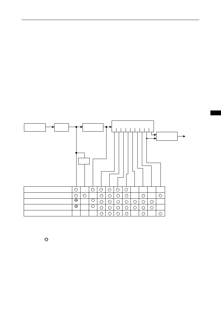
9-1
9
MSM66591/ML66592 User's Manual
Chapter 9 Time Base Counter (TBC)
9.
Time Base Counter (TBC)
The MSM66591/ML66592 time base counter (TBC) is an 8-bit counter that uses as its
input clock an overflow of the 4-bit auto-reload timer. The 4-bit auto-reload timer uses
as its input the master clock pulse (CLK) generated by multiplying the original oscillation
clock by 2.
The divided output of the TBC is used as the reference clock for the flexible timer, the
timer for the serial port, and others.
The TBC is cleared to "0" at reset (when the
RES
signal is input, the BRK instruction is
executed, the watchdog timer (WDT) is overflown, or an operation code trap is gener-
ated), and from then on operates unless the supply of the original oscillation clock
stops.
Figure 9-1 shows the configuration of TBC.
Figure 9-1 Configuration of TBC
*1
CLK (" " in the above figure) used for TM0 and TM1 is supplied to the timer data
sequencer and to the timing controller of each timer register module.
*2
If the 1/n (4-bit) counter is set as n = 1, and if the TBCCLK is selected for TM0 and TM1,
the flexible timer does not operate normally. (However, the freerun counters TM0,
TM0L, and TM1 operate normally.)
TBCCLK
PWM
8-Bit Timer for SCI
TM0 (20-Bit Timer)
TM1 (16-Bit Timer)
General-Purpose 8-Bit Timer
1/n (4-bit)
TBC (9-bit)
WDT (9-bit)
Reset
by WDT
1/2
1/2 CLK
1/2 TBCCLK
1/4 TBCCLK
1/8 TBCCLK
1/16 TBCCLK
1/32 TBCCLK
1/64 TBCCLK
1/128 TBCCLK
1/256 TBCCLK
CLK
*2
*2
*1
*1
Multiplied
by 2
Original
Osc. Clock
9-2
MSM66591/ML66592 User's Manual
Chapter 9 Time Base Counter (TBC)
9.1
1/n Counter
The MSM66591/ML66592 have a 4-bit auto-reload timer that uses a CLK as the input
clock, therefore the same clock pulse (TBCCLK) can be supplied to TBC, even if the
original oscillation frequency is changed.
The 1/n counter consists of a 4-bit counter (TBCKDVC) and a 4-bit register (TBCKDVR)
to store reload values.
TBCKDVC
TBCKDVC is a 4-bit counter that uses a CLK (clock generated by multiplying the
original oscillation clock by 2) as the input clock. Write is invalid. Read is valid, but the
high-order 4 bits will read "1" if read. At reset (when the
RES
signal is input, the BRK
instruction is executed, the watchdog timer is overflown, or an operation code trap is
generated), TBCKDVC becomes F0H.
TBCKDVR
TBCKDVR is a 4-bit register that stores reload values into TBCKDVC.
Write is valid, but write to high-order 4 bits is invalid. Read is valid, but the high order 4
bits will read "1" if read.
At reset (when the
RES
signal is input, the BRK instruction is executed, the watchdog
timer is overflown, or an operation code trap is generated), TBCKDVR becomes F0H.
At reset the 1/n counter divides the 1 CLK into 16, and supplies a 1/16 CLK to TBC as
TBCCLK.
After writing a reload value to TBCKDVR, the dividing operation may delay for a maxi-
mum of 16 clocks of CLK, depending on the dividing ratio written to TBCKDVR.
The following table shows 1/n counter correspondence between the dividing ratios and
the values to be set to TBCKDVR.
Dividing ratio
Value to TBCKDVR
Dividing ratio
Value to TBCKDVR
1/1
FFH
1/2
FEH
1/3
FDH
1/4
FCH
1/5
FBH
1/6
FAH
1/7
F9H
1/8
F8H
1/9
F7H
1/10
F6H
1/11
F5H
1/12
F4H
1/13
F3H
1/14
F2H
1/15
F1H
1/16
F0H
--
--
--
--
7
6
5
4
3
2
1
0
--
--
--
--
7
6
5
4
3
2
1
0

Watchdog Timer (WDT)
Chapter 10
10

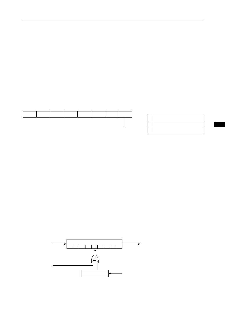
10-1
10
MSM66591/ML66592 User's Manual
Chapter 10 Watchdog Timer (WDT)
10. Watchdog Timer (WDT)
The watchdog timer (WDT) is a 9-bit counter that uses the overflow (1/256 TBCCLK or
1/512 TBCCLK) of the time base counter (TBC) as the input clock. It resets the device
when program runaway is detected. The contents of the WDT can be cleared to "0" by
the program, but the contents cannot be read or written.
10.1 WDT Control Register (WDTCON)
WDTCON is a 1-bit register that selects the WDT input clock.
Figure 10-1 shows the configuration of WDTCON.
Figure 10-2 Block Diagram of WDT
Overflow of TBC
Reset request by WDT
WDT Counter
WDT Register
WDT reset by writing "C3H", "3CH" alternately
CLEAR
Reset
0
1
2
3
4
5
6
7
8
(1/256 TBCCLK
or 1/512 TBCCLK)
Figure 10-1 Configuration of WDTCON
10.2 Operation of WDT
1/256 TBCCLK or 1/512 TBCCLK can be selected for the WDT input clock by the
WDTSEL bit (bit 0) of the WDT control register (WDTCON).
The WDT stops its function at reset (when the
RES
signal is input, the BRK instruction
is executed, the WDT is overflown, and an operation code trap is generated).
The WDT is started by writing "3CH" to WDT (SFR address 27H) on SFR by the
program. The WDT is cleared to "0" by writing "C3H" and "3CH" to WDT alternately.
If the WDT overflows, the CPU performs a reset process and 2 bytes of the content of
the branch address stored in addresses 0004H≠0005H (vector address of reset by
WDT) are loaded to the program counter.
Figure 10-2 shows a block diagram of WDT.
"--" indicates a bit that is not provided.
"1" is read if a read instruction is executed.
WDTCON
7
6
5
4
3
2
1
0
--
--
--
--
--
--
--
WDTSEL
WDT input clock
0
1/256 TBCCLK
1
1/512 TBCCLK

10-2
MSM66591/ML66592 User's Manual
Chapter 10 Watchdog Timer (WDT)
10.3 Time until Overflow of WDT
When the master clock is f MHz and 1/256 TBCCLK is selected:
t
WDT
= (1/f)
µ
sec
•
n
•
2
8
•
2
9
n is the dividing value of the 4-bit auto-reload timer (1/n counter) of the TBC input.
If the WDT is cleared, a minus error of a maximum of
t
WDT
= (1/f)
µ
sec
•
n
•
2
8
occurs, since the content of TBC does not change.
When the master clock of the MSM66591 is 24 MHz and n = 8, the result is
t
WDT
= 43.69 msec
t
WDT
= 85.33
µ
sec
When the master clock of the ML66592 is 28 MHz and n = 8, the result is
t
WDT
= 37.45 msec
t
WDT
= 73.14
µ
sec
10.4 Program Runaway Detection Timing Diagram
Figure 10-3 (a) shows an example of timing when a program is executed normally.
Figure 10-3 (b) shows an example of timing when program runaway occurs. Figure 10-
4 (a), (b), and (c) show examples of program runaway.
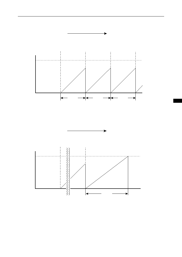
10-3
10
MSM66591/ML66592 User's Manual
Chapter 10 Watchdog Timer (WDT)
Figure 10-3 Example of Timing When Program Runaway is Detected
Progress of Program
Content of WDT
3CH write
WDT start
C3H write
WDT clear to "0"
3CH write
WDT clear to "0"
C3H write
WDT clear to "0"
within
t
WDT
within
t
WDT
within
t
WDT
(a) When program is executed normally
Content of WDT
3CH write
WDT start
C3H write
WDT clear to "0"
Overflow occurred
Reset by WDT
t
WDT
(b) When program runaway occurs
OVF
000H
OVF
000H
t
t
Progress of Program
10-4
MSM66591/ML66592 User's Manual
Chapter 10 Watchdog Timer (WDT)
Figure 10-4 Examples of Program Runaway
(a) Executes only a 3CH write
(b) Executes only a C3H write
(c) No writing to WDT
: Progress of program during
an abnormal execution
: Progress of program during
a normal execution
WDT is cleared to "0"
by writing 3CH to WDT
WDT is cleared to "0"
by writing C3H to WDT
WDT is cleared to "0"
by writing 3CH to WDT
WDT is cleared to "0"
by writing C3H to WDT
WDT is cleared to "0"
by writing 3CH to WDT
WDT is cleared to "0"
by writing C3H to WDT

Flexible Timer (FTM)
Chapter 11
11
11

11-1
11
11
MSM66591/ML66592 User's Manual
Chapter 11 Flexible Timer (FTM)
11. Flexible Timer (FTM)
The MSM66591/ML66592 flexible timer (FTM) consists of a 20-bit counter, a 16-bit
counter, four 20-bit registers, fourteen 16-bit registers, control registers, and other
components.
The functions of the timer include:
∑ 20-bit capture modes: 4 (type A1)
∑ 16-bit capture modes: 2 (type A2)
∑ double buffer real-time output modes: 10 (type B)
∑ capture/real-time output mode (with 4-port RTO): 1 (type D)
∑ capture/real-time output mode: 1 (type E)
Figure 11-1 shows the configuration of FTM.
Table 11-1 shows the list of SFRs for controlling FTM.
11-2
MSM66591/ML66592 User's Manual
Chapter 11 Flexible Timer (FTM)
Figure 11-1 Configuration of FTM
P3_4/CAP0≠P3_7/CAP3
P2_0/RTO4≠P2_7/RTO11
P10_0/RTO12, P10_1/RTO13
P10_2/CAP14, P10_3/CAP15
P3_0/FTM17A
P3_1/FTM17B≠P3_3/FTM17D
Internal Bus
Counter Part
TM0 (20-bit)
TM1 (16-bit)
TMCON (8-bit)
Counter Selection Part
TMSEL (16-bit)
TMSEL2 (8-bit)
Type A1 Register Modules
TMR0≠TMR3
TMRL0≠TMRL3
CAPCON
EVDV0≠EVDV3
EVDV0BF≠EVDV3BF
EVNTCONL,
EVNTCONH
Type A2 Register Modules
TMR14, TMR15
CAPCON
RTOCON14, RTOCON15
EVNTCON2
Type D Register Module
TMR17
TMRMODE
RTOCON17, RTO4CON
CAPCON
Type B Register Modules
TMR4≠TMR13
TMR4BF≠TMR13BF
RTOCON4≠RTOCON13
P10_4/FTM16
Type E Register Module
TMR16
TMRMODE
RTOCON16
CAPCON
11-3
11
11
MSM66591/ML66592 User's Manual
Chapter 11 Flexible Timer (FTM)
Table 11-1 List of SFRs for Controlling FTM
008A
--
TMR0
Timer Register 0
Undefined
16
R
008B
008C
008D
008E
008F
0090
0091
0092
0093
0094
0095
0096
0097
0098
0099
009A
009B
009C
009D
009E
009F
00A0
00A1
00A2
00A3
00A4
00A5
00A6
00A7
00A8
00A9
00AA
00AB
00AC
00AD
00AE
00AF
00B0
00B1
00B2
00B3
00B4
00B5
Timer Register 1
Timer Register 2
Timer Register 3
Timer Register 4
Timer Register 5
Timer Register 6
Timer Register 7
Timer Register 8
Timer Register 9
Timer Register 10
Timer Register 11
Timer Register 12
Timer Register 13
Timer Register 14
Timer Register 15
Timer Register 16
Timer Register 17
TMR4 Buffer Register
TMR5 Buffer Register
TMR6 Buffer Register
TMR7 Buffer Register
--
--
--
--
--
--
--
--
--
--
--
--
--
--
--
--
--
--
--
--
--
TMR1
TMR2
TMR3
TMR4
TMR5
TMR6
TMR7
TMR8
TMR9
TMR10
TMR11
TMR12
TMR13
TMR14
TMR15
TMR16
TMR17
TMR4BF
TMR5BF
TMR6BF
TMR7BF
R/W
Undefined
Undefined
Undefined
0000
0000
0000
0000
0000
0000
0000
0000
0000
0000
Undefined
Undefined
0000
0000
0000
0000
0000
0000
R
R/W
Address [H]
Name
Abbreviated
Name (BYTE)
R/W
8/16-Bit
Operation
Reset
State [H]
Abbreviated
Name (WORD)

11-4
MSM66591/ML66592 User's Manual
Chapter 11 Flexible Timer (FTM)
00BA
00BC
00BE
00BB
00BD
00BF
TMR10 Buffer Register
--
TMR10BF
TMR11 Buffer Register
--
TMR11BF
TMR12 Buffer Register
--
TMR12BF
0000
0000
0000
R/W
16
00C0
RTO Control Register 17
--
0000
8
TMR13 Buffer Register
8
00C1
00C2
00C3
00C4
00C6
00C7
00C8
00C9
00CA
00CB
00CC
00CD
00CE
00CF
00D0
00D1
00D2
00D3
00D4
00D5
00D6
00D7
00D8
00D9
00DA
00DB
Timer Setting Register
Timer Setting Register 2
RTO Control Register 4
RTO Control Register 5
RTO Control Register 6
RTO Control Register 7
RTO Control Register 8
RTO Control Register 9
RTO Control Register 10
RTO Control Register 11
RTO Control Register 12
RTO Control Register 13
RTO Control Register 16
Timer Counter 0
Timer Counter 1
TMR0 Low-order 4 Bits
TMR1 Low-order 4 Bits
TMR2 Low-order 4 Bits
TMR3 Low-order 4 Bits
--
--
TMSEL2
RTOCON4
RTOCON5
RTOCON6
RTOCON7
RTOCON8
RTOCON9
RTOCON10
RTOCON11
RTOCON12
RTOCON13
RTOCON16
--
--
--
--
--
--
--
--
--
--
--
--
TMSEL
TMR13BF
0000
0000
FC
F8
F8
F8
F8
F8
F8
F8
F8
F8
F8
F8
RTOCON17
--
TM0L
--
TM0
--
TM1
0000
TMR0L
Undefined
--
TMR1L
Undefined
--
TMR2L
Undefined
--
TMR3L
Undefined
--
R/W
4-Port RTO Control Register
Timer Counter 0 Low-order 4 Bits
RTO4CON
--
16
8
R/W
F8
00
0F
16
R
Some addresses are not consecutive.
Addresses in the address column marked by "" indicate that the register has bits missing.
00B6
00B7
00B8
00B9
TMR8 Buffer Register
TMR9 Buffer Register
--
--
TMR8BF
TMR9BF
0000
0000
Address [H]
Name
Abbreviated
Name (BYTE)
R/W
8/16-Bit
Operation
Reset
State [H]
Abbreviated
Name (WORD)
Table 11-1 List of SFRs for Controlling FTM (continued)
11-5
11
11
MSM66591/ML66592 User's Manual
Chapter 11 Flexible Timer (FTM)
Table 11-1 List of SFRs for Controlling FTM (continued)
Event Dividing Counter 1
0170
0171
0172
0173
0174
0175
0176
0177
0178
0179
017A
017B
Event Dividing Counter 0
Event Dividing Counter 2
Event Dividing Counter 3
Event Dividing Counter 15
EVDV0 Buffer Register
EVDV1 Buffer Register
EVDV3 Buffer Register
EVDV14 Buffer Register
EVDV0
C0
--
EVDV1
C0
--
EVDV2
C0
--
EVDV3
C0
--
EVDV15
C0
--
EVDV0BF
C0
--
EVDV1BF
C0
--
EVDV3BF
C0
--
EVDV14BF
C0
--
EVDV15BF
C0
--
8
R/W
Event Dividing Counter 14
EVDV2 Buffer Register
EVDV15 Buffer Register
EVDV2BF
--
EVDV14
--
C0
C0
017C
017D
017E
--
CAPCON
Capture Control Register
TMR Mode Register
TMRMODE
--
F2
8
16
0000
R/W
Some addresses are not consecutive.
Addresses in the address column marked by "" indicate that the register has bits missing.
00DC
00DD
00DE
00DF
Timer Control Register
Event Control Register 2
Event Control Register L
Event Control Register H
TMCON
00
--
EVNTCON2
88
--
EVNTCONL
88
--
EVNTCONH
88
--
Address [H]
Name
Abbreviated
Name (BYTE)
R/W
8/16-Bit
Operation
Reset
State [H]
Abbreviated
Name (WORD)
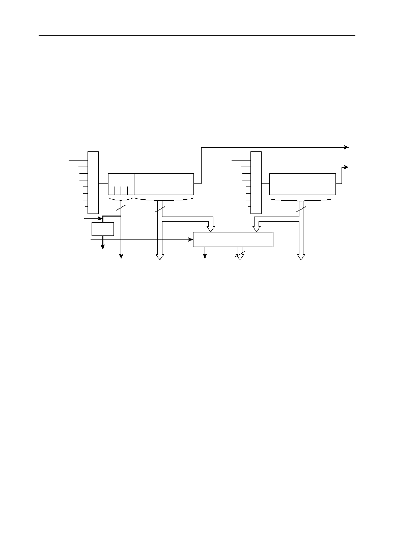
11-6
MSM66591/ML66592 User's Manual
Chapter 11 Flexible Timer (FTM)
Figure 11-2 Configuration of Counter Part
TBCCLK
1/2 TBCCLK
1/4 TBCCLK
1/8 TBCCLK
1/16 TBCCLK
1/32 TBCCLK
1/64 TBCCLK
1/128 TBCCLK
TBCCLK
1/2 TBCCLK
1/4 TBCCLK
1/8 TBCCLK
1/16 TBCCLK
1/32 TBCCLK
1/64 TBCCLK
1/128 TBCCLK
Selector
Selector
TM0
TM0L
TM1
0
3 4
15
4 bits
16 bits
CLK
TM0L4
To type A1 timer register module
TMDS
TMD
To each timer register module
Timer Data Sequencer
16 bits
16 bits
OVF Interrupt
0
19
Internal Bus
Internal Bus
Internal
Bus
4-bit
Latch
TM read
11.1 Configuration of Counter Part
The counter part consists of a 20-bit freerun counter (TM0, TM0L), a 16-bit freerun
counter (TM1), an input clock selector for each freerun counter, a timer data sequencer
to output as TMD the high-order 16-bits of TM0 and the TM1 values alternately at one-
CLK intervals, and a control register (TMCON) to control the operation of TM0/TM1.
TM0 and TM1 generate interrupt requests when an overflow occurs.
Figure 11-2 shows the configuration of the counter part.
Timer 0 is a 20-bit counter, the low-order 4 bits are TM0L, and the high-order 16 bits
are TM0, and can be read/written by the program. However, if TM0 is read, the con-
tents of TM0L are latched to the temporary register at the same time. If TM0L is read
after that, the latched contents are read. Therefore if the data of Timer 0 is read in 20-
bit length, read TM0 first, then TM0L. If TM0L is written, the low-order 4-bits are invalid.
If TM0L is read, all "1s" are read from the low-order 4 bits. TM1 is a 16-bit counter, and
can be read/written by the program.
At reset (when the
RES
signal is input, the BRK instruction is executed, the watchdog
timer is overflown, or an operation code trap is generated), TM0 and TM1 become
0000H, TM0L becomes 0FH, and operation is stopped.
The input clocks of TM0L, TM0, and TM1 are selected as TBCCLK or 1/2 TBCCLK to
1/128 TBCCLK by the timer control register (TMCON).
TMCON is an 8-bit register, that selects the count clock of TM0L, TM0 and TM1, and
also selects run/stop. At reset (when the
RES
signal is input, the BRK instruction is
executed, the watchdog timer is overflown, or an operation code trap is generated),
TMCON becomes 00H, TBCCLK is selected for the count clock of TM0L, TM0 and
TM1, and operation is stopped.
11-7
11
11
MSM66591/ML66592 User's Manual
Chapter 11 Flexible Timer (FTM)
TM0CK
TM0 Count Clock
2 1 0
0 0 0 TBCCLK
0 0 1 1/2 TBCCLK
0 1 0 1/4 TBCCLK
0 1 1 1/8 TBCCLK
1 0 0 1/16 TBCCLK
1 0 1 1/32 TBCCLK
1 1 0 1/64 TBCCLK
1 1 1 1/128 TBCCLK
0 TM0 count operation stops
1 TM0 count runs
0 TM1 count operation stops
1 TM1 count runs
TM1CK
TM1 Count Clock
2 1 0
0 0 0 TBCCLK
0 0 1 1/2 TBCCLK
0 1 0 1/4 TBCCLK
0 1 1 1/8 TBCCLK
1 0 0 1/16 TBCCLK
1 0 1 1/32 TBCCLK
1 1 0 1/64 TBCCLK
1 1 1 1/128 TBCCLK
TM1RUN TM1CK2 TM1CK1 TM1CK0 TM0RUN TM0CK2 TM0CK1 TM0CK0
7
6
5
4
3
2
1
0
TMCON
Figure 11-3 Configuration of TMCON
TM0
TM1
TM0
TM1
TM0
TM1
TM0
CLK
TMDS
TMD
Figure 11-4 Output of Timer Data Sequencer
The 4-bit output (TM0L4) of TM0L is connected to the timer register module type A1.
The high-order 16-bit output of TM0, and the 16-bit output of TM1 are time-sharing
outputs (TMD) by CLK, at the timer data sequencer, and are connected to each timer
register module.
Figure 11-3 shows the configuration of TMCON, and Figure 11-4 shows the timing of
the timer data sequencer.

11-8
MSM66591/ML66592 User's Manual
Chapter 11 Flexible Timer (FTM)
11.2 Counter Selection Part
The MSM66591/ML66592 have 18 timer register modules. Each timer register module
can be connected to either one of the two freerun counters (TM0 and TM1). The
selection is specified by the timer setting register (TMSEL) and timer setting register 2
(TMSEL2). TMSEL is a 16-bit register and TMSEL2 is a 2-bit register, both of which are
read/write enabled. Timer register 0 (TMR0) through timer register 3 (TMR3) consist of
20 bits. TM0L4 is always connected to the low-order 4 bits regardless of the specifica-
tion of TMSEL.
"1s" are read from bits 7≠2 when TMSEL2 is read.
Note that bit manipulation instructions such as SB and RB cannot be used, because
TMSEL has only 16-bit access.
At reset (when the
RES
signal is input, the BRK instruction is executed, the watchdog
timer is overflown, or an operation code trap is generated), TMSEL and TMSEL2
become 0000H and FCH respectively, and all timer register modules are connected to
TM0.
Figure 11-5 shows the configuration of TMSEL, and Figure 11-6 the configuration of
TMSEL2.
11-9
11
11
MSM66591/ML66592 User's Manual
Chapter 11 Flexible Timer (FTM)
7
6
5
4
3
2
1
0
0 TMR0 is connected to TM0
1 TMR0 is connected to TM1
0 TMR1 is connected to TM0
1 TMR1 is connected to TM1
0 TMR2 is connected to TM0
1 TMR2 is connected to TM1
0 TMR3 is connected to TM0
1 TMR3 is connected to TM1
0 TMR4 is connected to TM0
1 TMR4 is connected to TM1
0 TMR5 is connected to TM0
1 TMR5 is connected to TM1
0 TMR6 is connected to TM0
1 TMR6 is connected to TM1
0 TMR7 is connected to TM0
1 TMR7 is connected to TM1
TMSEL (bits 0≠7)
Figure 11-5 Configuration of TMSEL
Figure 11-6 Configuration of TMSEL2
15
14
13
12
11
10
9
8
0 TMR8 is connected to TM0
1 TMR8 is connected to TM1
0 TMR9 is connected to TM0
1 TMR9 is connected to TM1
0 TMR10 is connected to TM0
1 TMR10 is connected to TM1
0 TMR11 is connected to TM0
1 TMR11 is connected to TM1
0 TMR12 is connected to TM0
1 TMR12 is connected to TM1
0 TMR13 is connected to TM0
1 TMR13 is connected to TM1
TMSEL (bits 8≠15)
0 TMR14 is connected to TM0
1 TMR14 is connected to TM1
0 TMR15 is connected to TM0
1 TMR15 is connected to TM1
--
--
--
--
--
--
T17SEL T16SEL
7 6 5 4 3 2 1 0
0 TMR16 is connected to TM0
1 TMR16 is connected to TM1
0 TMR17 is connected to TM0
1 TMR17 is connected to TM1
"--" indicates a bit that is not provided.
"1" is read if a read instruction is executed.
TMSEL2 (bits 0≠7)
11-10
MSM66591/ML66592 User's Manual
Chapter 11 Flexible Timer (FTM)
11.3 Type A1 Register Modules (TMR0≠TMR3)
The MSM66591/ML66592 have four sets of type A1 register modules (TMR0≠TMR3).
The configuration is the same for all the sets, except for the address of registers on
SFR.
11.3.1 Configuration of Type A1 Register Modules (TMR0≠TMR3)
Type A1 register modules have a capture input function. Figure 11-7 shows the configu-
ration of a type A1 register module.
Type A1 register modules consist of a 20-bit timer register (TMRn, TMRnL), a pin to
input external events (CAPn), the edge detection of an external event, a divider to
divide an external event, a timing controller, and control registers (CAPCON,
EVNTCONL, EVNTCONH) to specify the operation of the valid edge of an external
event and the operation of a divider.
If CAP0≠CAP3 pins are used as a capture function, set the bit corresponding to the
Port 3 secondary function control register to "1".
Figure 17-1 shows the configuration of type A1 register module.
Figure 11-7 Configuration of Type A1 Register Module
[1]
Timer Registers (TMR0, TMR0L≠TMR3, TMR3L)
The timer register consists of 20 bits, that are divided into high-order 16 bits (TMR0≠
TMR3) and low-order 4 bits (TMR0L≠TMR3L). The counter specified by TMSEL is
connected to TMR0≠TMR3, and the low-order 4 bits of the 20-bit counter are always
connected to TMR0L≠TMR3L.
If the specified valid edge is input to CAP0≠CAP3 pins for the specified number of
pulses, a capture event is generated. In that case, the 16-bits of the content of the
counter specified by TMSEL are loaded to TMR0L≠TMR3L, and the content of the low-
order 4 bits of the 20-bit counter is loaded to TMR0L≠TMR3L.
TMR0≠TMR3 and TMR0L≠TMR3L cannot be written, but can be read by the program.
However, if TMR0L≠TMR3L are read, the high-order 4 bits are valid, and "1" is read
from the low-order 4 bits.
CAPCON
TMRn
CAPn input
Edge
Detection n
Dividing
Circuit n
Timing
Controller n
CLK
TnSEL
TMDS
TMD
TM0L4
19
12
4 3
n = 0≠3
Interrupt
EVNTCONL,
EVNTCONH
TMRnL
0
1
1
1
1

11-11
11
11
MSM66591/ML66592 User's Manual
Chapter 11 Flexible Timer (FTM)
At reset (when the
RES
signal is input, the BRK instruction is executed, the watchdog
timer is overflown, or an operation code trap is generated), TMR0≠TMR3 and TMR0L≠
TMR3L become undefined.
[2]
Capture Control Register (CAPCON)
CAPCON is a 16-bit register that specifies the valid edge of a signal that is input to the
CAP0 (P3_4)≠CAP3 (P3_7) pins, CAP14 (P10_2), CAP15 (P10_3), and, when TMR16
and TMR17 are in CAP mode, to FTM16 (P10_4) and FTM17A (P3_0) pins. Bits 0 to 7
of CAPCON are used to specify the valid edge of the signal that is input to the CAP0
(P3_4)≠CAP3 (P3_7) pins.
Since CAPCON has only 16-bit access, bit manipulation instructions such as SB and
RB cannot be used.
At reset (when the
RES
signal is input, the BRK instruction is executed, the watchdog
timer is overflown, or an operation code trap is generated), CAPCON becomes 0000H,
and CAP0≠CAP3, CAP14, CAP15, FTM16, and FTM17A are specified to the falling
edge.
Figure 11-8 shows the configuration of bits 0≠7 of CAPCON.
Figure 11-8 Configuration of Bits 0≠7 of CAPCON
7
6
5
4
3
2
1
0
CAPCON (bits 0≠7)
"*" indicates either "1" or "0".
Bit
Valid edge of CAP0
1
0
0
*
1
0
1
1
Falling edge
Rising edge
Both edges
Bit
Valid edge of CAP1
3
2
0
*
1
0
1
1
Falling edge
Rising edge
Both edges
Bit
Valid edge of CAP2
5
4
0
*
1
0
1
1
Falling edge
Rising edge
Both edges
Bit
Valid edge of CAP3
7
6
0
*
1
0
1
1
Falling edge
Rising edge
Both edges
8
11-12
MSM66591/ML66592 User's Manual
Chapter 11 Flexible Timer (FTM)
[3]
Event Control Registers (EVNTCONL, EVNTCONH)
EVNTCONL and EVNTCONH are 8-bit registers that specify the dividing ratio (1/1, 1/2,
1/4, 1/8, 1/16, 1/32, 1/64) of the valid edge that is specified by the CAPCON of the
signal that is input to CAP0 (P3_4)≠CAP3 (P3_7) pins.
At reset (when the
RES
signal is input, the BRK instruction is executed, the watchdog
timer is overflown, or an operation code trap is generated), both EVNTCONL and
EVNTCONH become 88H, and a 1/1 division is specified.
Figure 11-9 shows the configuration of EVNTCONL, and Figure 11-10 the configuration
of EVNTCONH.
--
T1EV2 T1EV1 T1EV0
--
T0EV2 T0EV1 T0EV0
T0EV
Dividing ratio of valid edge of CAP0 pin
2 1 0
0 0 0 1/1 division
0 0 1 1/2 division
0 1 0 1/4 division
0 1 1 1/8 division
1 0 0 1/16 division
1 0 1 1/32 division
1 1
* 1/64 division
7
6
5
4
3
2
1
0
T1EV
Dividing ratio of valid edge of CAP1 pin
2 1 0
0 0 0 1/1 division
0 0 1 1/2 division
0 1 0 1/4 division
0 1 1 1/8 division
1 0 0 1/16 division
1 0 1 1/32 division
1 1
* 1/64 division
"--" indicates a bit that is not provided.
"1" is read if a read instruction is executed.
"*" indicates either "1" or "0".
EVNTCONL
Figure 11-9 Configuration of EVNTCONL

11-13
11
11
MSM66591/ML66592 User's Manual
Chapter 11 Flexible Timer (FTM)
--
T3EV2 T3EV1 T3EV0
--
T2EV2 T2EV1 T2EV0
T2EV
Dividing ratio of valid edge of CAP2 pin
2 1 0
0 0 0 1/1 division
0 0 1 1/2 division
0 1 0 1/4 division
0 1 1 1/8 division
1 0 0 1/16 division
1 0 1 1/32 division
1 1
* 1/64 division
7
6
5
4
3
2
1
0
T3EV
Dividing ratio of valid edge of CAP3 pin
2 1 0
0 0 0 1/1 division
0 0 1 1/2 division
0 1 0 1/4 division
0 1 1 1/8 division
1 0 0 1/16 division
1 0 1 1/32 division
1 1
* 1/64 division
EVNTCONH
"--" indicates a bit that is not provided.
"1" is read if a read instruction is executed.
"*" indicates either "1" or "0".
Figure 11-10 Configuration of EVNTCONH

11-14
MSM66591/ML66592 User's Manual
Chapter 11 Flexible Timer (FTM)
[4]
Event Dividing Counters 0≠3 (EVDV0≠EVDV3)
EVDV0≠EVDV3 are 6-bit counters that count the valid edge (specified by CAPCON)
input to CAP0≠CAP3 pins for the value specified by EVNTCONL and EVNTCONH.
Figure 11-11 shows the configuration of EVDVn (n = 0≠3).
Figure 11-11 Configuration of EVDVn (n = 0≠3)
Whatever data is written to EVDV0≠EVDV3, the counter is cleared to "0". Read is valid,
but "1" is read from the high-order 2 bits. EVDV0≠EVDV3 are cleared to "0" when a
capture event is generated.
At reset (when the
RES
signal is input, the BRK instruction is executed, a watchdog
timer is overflown, or an operation code trap is generated), EVDV0≠EVDV3 become
C0H.
[5]
EVDV0≠EVDV3 Buffer Registers (EVDV0BF≠EVDV3BF)
EVDV0BF≠EVDV3BF are 6-bit registers that hold the content of EVDV0≠EVDV3
(content just prior to being cleared to "0") when a capture event is generated.
Figure 11-12 shows the configuration of EVDVnBF (n = 0≠3).
Figure 11-12 Configuration of EVDVnBF (n = 0≠3)
Write to EVDV0BF≠EVDV3BF is valid, however write to the high-order 2-bits is invalid.
Read is valid, however "1" is read from the high-order 2-bits.
If the content of EVNTCONL or EVNTCONH is updated and the dividing ratio is
changed during a capture operation, it is necessary to check whether an interrupt was
generated based on normal dividing, by testing the content of EVDVnBF at the begin-
ning of the capture interrupt process program.
At reset (when the
RES
signal is input, the BRK instruction is executed, the watchdog
timer is overflown, or an operation code trap is generated), EVDV0BF≠EVDV3BF
become C0H.
7
6
5
4
3
2
1
0
EVDVn
--
--
7
6
5
4
3
2
1
0
EVDVnBF
--
--

11-15
11
11
MSM66591/ML66592 User's Manual
Chapter 11 Flexible Timer (FTM)
11.3.2 Operation of Type A1 Register Modules (TMR0≠TMR3)
If the valid edge specified by CAPCON is input to CAP0≠CAP3 pins when the TM
specified by TMSEL is in RUN status, the divider divides the pulse in the dividing ratio
specified by EVNTCON. In that case, an interrupt request by a capture event is gener-
ated, and at the same time, the content of the counter specified by TMSEL is loaded to
TMRn, and the content of TM0L4 is loaded to TMRnL. Also the content of the dividing
counter in the divider is loaded to buffer register EVDVnBF, and the content of the
dividing counter EVDVn is cleared to "0". Input a capture event at the interval of 3 CLKs
or more. (Capture operation may be performed only once even if the capture event is
input twice or more at an interval of less than 3 CLKs.)
Figure 11-13 (a) and (b) shows capture operation timing examples.
Figure 11-13 (a) Capture Operation Timing Example
Figure 11-13 (b) Capture Operation Timing Example
a
b
c
d
e
a
b
c
d
e
Interrupt
request is
generated
Interrupt
request is
generated
Interrupt
request is
generated
Interrupt
request is
generated
Interrupt
request is
generated
CAPn input (fall, 1/1 dividing)
OVF
Content of counters (TM0, TM1)
0H
Content of TMRn, TMRnL
0
1
2
3
0
1
0
1
0
1
0
1
0
1
2
3
0
1
3
3
1
1
1
1
3
a
b
c
d
e
f
g
a
b
c
d
e
f
g
CAPn input (rise)
OVF
Content of counters (TM0, TM1)
0H
Content of TMRn, TMRnL
Content of EVDVn
Content of EVDVnBF
1/4 dividing
1/2 dividing
1/4 dividing
Interrupt
request is
generated
Interrupt
request is
generated
Interrupt
request is
generated
Interrupt
request is
generated
Interrupt
request is
generated
Interrupt
request is
generated
Interrupt
request is
generated

11-16
MSM66591/ML66592 User's Manual
Chapter 11 Flexible Timer (FTM)
If TM1 is selected as the timer for connecting to type A1 register module, 4 bits of TM0L
are latched to TMRnL at the time TM1 is latched to TMRn.
Type A1 register modules have no "function to check a cycle of the timer counter
between capture events," which is used for the capture function of type D and E register
modules.
11.3.3 Capture Pin Dividing Circuit
The MSM66591/ML66592 type A1 timer register modules have a capture pin dividing
circuit that can perform division from 1/1 to 1/64.
[1]
Configuration of Dividing Circuit
The dividing circuit consists of the following:
∑ counter to divide valid pulses input to capture pin (EVDVn) (n = 0≠3)
∑ register to set dividing ratio (EVNTCONL, EVNTCONH)
∑ comparison circuit to compare counter value and register value
∑ register to hold dividing counter value when an event is generated (EVDVnBF) (n =
0≠3)
[2]
Operation of Dividing Circuit
If valid edges (pulses) are input to a capture pin, EVDVn counts their number. If the
counter value and the dividing value specified by EVNTCONL or EVNTCONH match, a
capture event is generated.
If a capture event is generated, a capture interrupt request is generated, the counter
value is loaded to the timer register, the EVDVn value is loaded to EVDVnBF, and
EVDVn is cleared to "0". (n = 0≠3)
[3]
Operation to Switch Dividing Ratio
Since the dividing ratio is programmable, the dividing operation may differ, depending
on the timing that changes the dividing ratio. In this case, the MSM66591/ML66592
operate as follows:
1) When the dividing ratio is changed from 1/N to 1/M (N > M), if a valid edge is input
to a capture pin when:
∑ counter value C in the dividing circuit is C
M ≠ 1 (except when M = 1)
or
∑ M = 1
a capture event is generated.
If a valid edge is input to a capture pin when:
∑ counter value C in the dividing circuit is C < M ≠ 1 (except when M = 1)
a capture event is not generated, and the counter value in the dividing circuit is
incremented.
2) When the dividing ratio is changed from 1/N to 1/M (N < M), the dividing operation
continues until the counter value becomes M, and a capture event is generated
when the counter value becomes M.
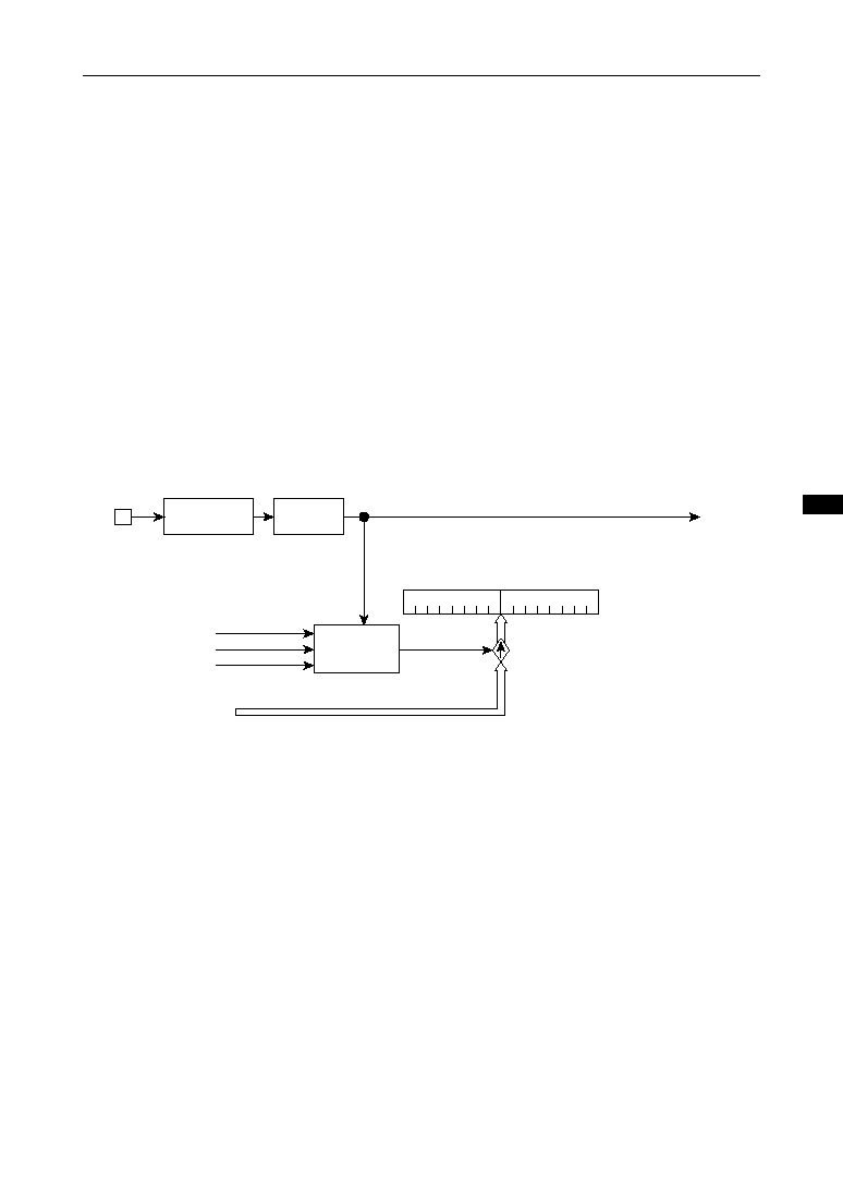
11-17
11
11
MSM66591/ML66592 User's Manual
Chapter 11 Flexible Timer (FTM)
11.4 Type A2 Register Modules (TMR14, TMR15)
The MSM66591/ML66592 have two sets of type A2 register modules (TMR14, TMR15).
The configuration is the same for the two sets, except for the address of registers on
SFR.
11.4.1 Configuration of Type A2 Register Modules (TMR14, TMR15)
Type A2 register modules have a 16-bit capture input function.
Type A2 register modules consist of a 16-bit timer register (TMRn), a pin to input
external events (CAPn), the edge detection of an external event, a divider to divide an
external event, a timing controller, and control registers (CAPCON, EVNTCON2) to
specify the operation of the valid edge of an external event and the operation of a
divider.
If CAP14 and CAP15 pins are used as a capture function, set the bit corresponding to
the Port 10 secondary function control register to "1".
Figure 11-14 shows the configuration of a type A2 register module.
Figure 11-14 Configuration of Type A2 Register Module
[1]
Timer Registers (TMR14, TMR15)
The timer registers consist of 16 bits. The counter specified by TMSEL is connected to
TMR14 and TMR15. If the specified valid edge is input to CAP14 and CAP15 for the
specified number of pulses, a capture event is generated. When a capture event is
generated, the 16-bit content of the counter specified by TMSEL is loaded into TMR14
and TMR15.
The program can read from but not write to TMR14 and TMR15.
At reset (when the
RES
signal is input, the BRK instruction is executed, the watchdog
timer is overflown, or an operation code trap is generated), TMR14 and TMR15 are
undefined.
CAPCON
TMRn
CAPn input
Edge
Detection n
Dividing
Circuit n
Timing
Controller n
CLK
TnSEL
TMDS
TMD
15
8
0
Interrupt
EVNTCON2
n = 14, 15
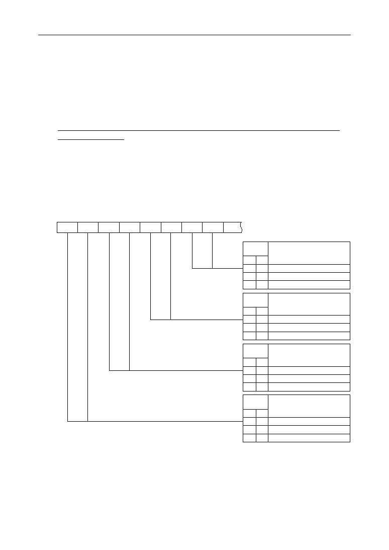
11-18
MSM66591/ML66592 User's Manual
Chapter 11 Flexible Timer (FTM)
[2]
Capture Control Register (CAPCON)
CAPCON is a 16-bit register that specifies the valid edge of a signal that is input to the
CAP0 (P3_4)≠CAP3 (P3_7) pins, CAP14 (P10_2), CAP15 (P10_3), and, when TMR16
and TMR17 are in CAP mode, to FTM16 (P10_4) and FTM17A (P3_0) pins. Bits 8 to 15
of CAPCON are used to specify the valid edge of the signal that is input to the CAP14
(P10_2), CAP15 (P10_3), FTM16 (P10_4), and FTM17A (P3_0) pins.
Since CAPCON has only 16-bit access, bit manipulation instructions such as SB and
RB cannot be used.
At reset (when the
RES
signal is input, the BRK instruction is executed, the watchdog
timer is overflown, or an operation code trap is generated), CAPCON becomes 0000H,
and CAP0≠CAP3, CAP14, CAP15, FTM16, and FTM17A are specified to the falling
edge.
Figure 11-15 shows the configuration of bits 8≠15 of CAPCON.
Figure 11-15 Configuration of Bits 8≠15 of CAPCON
14
13
12
11
10
9
8
7
Bit
Valid edge of CAP14
1
0
0
*
1
0
1
1
Falling edge
Both edges
Rising edge
Bit
Valid edge of CAP15
3
2
0
*
1
0
1
1
Falling edge
Both edges
Rising edge
Bit
Valid edge of FTM16
(when in CAP mode)
5
4
0
*
1
0
1
1
Falling edge
Both edges
Rising edge
Bit
Valid edge of FTM17
(when in CAP mode)
7
6
0
*
1
0
1
1
Falling edge
Both edges
Rising edge
15
CAPCON (bits 8≠15)
"*" indicates either "1" or "0".

11-19
11
11
MSM66591/ML66592 User's Manual
Chapter 11 Flexible Timer (FTM)
[3]
Event Control Register 2 (EVNTCON2)
EVNTCON2 is an 8-bit register that specifies the dividing ratio (1/1, 1/2, 1/4, 1/8, 1/16,
1/32, 1/64) of the valid edge that is specified by the CAPCON of the signal that is input
to CAP14 (P10_2) and CAP15 (P10_3) pins.
At reset (when the
RES
signal is input, the BRK instruction is executed, the watchdog
timer is overflown, or an operation code trap is generated), EVNTCON2 becomes 88H,
and a 1/1 division is specified.
Figure 11-16 shows the configuration of EVNTCON2.
Figure 11-16 Configuration of EVNTCON2
--
T15EV2 T15EV1 T15EV0
--
T14EV2 T14EV1 T14EV0
T14EV
Dividing ratio of valid edge of CAP14 pin
2 1 0
0 0 0 1/1 division
0 0 1 1/2 division
0 1 0 1/4 division
0 1 1 1/8 division
1 0 0 1/16 division
1 0 1 1/32 division
1 1
* 1/64 division
7
6
5
4
3
2
1
0
T15EV
Dividing ratio of valid edge of CAP15 pin
2 1 0
0 0 0 1/1 division
0 0 1 1/2 division
0 1 0 1/4 division
0 1 1 1/8 division
1 0 0 1/16 division
1 0 1 1/32 division
1 1
* 1/64 division
"--" indicates a bit that is not provided.
"1" is read if a read instruction is executed.
"*" indicates either "1" or "0".
EVNTCON2

11-20
MSM66591/ML66592 User's Manual
Chapter 11 Flexible Timer (FTM)
7
--
6
--
5
4
3
2
1
0
EVDVn
7
--
6
--
5
4
3
2
1
0
EVDVnBF
[4]
Event Dividing Counters 14, 15 (EVDV14, EVDV15)
EVDV14 and EVDV15 are 6-bit counters that count the valid edge (specified by
CAPCON) input to CAP14 and CAP15 pins for the value specified by EVNTCON2.
Figure 11-17 shows the configuration of EVDVn (n = 14, 15).
Figure 11-17 Configuration of EVDVn (n = 14, 15)
Whatever data is written to EVDV14 and EVDV15, the counter is cleared to "0". Read is
valid, but "1" is read from the high-order 2 bits. EVDV14 and EVDV15 are cleared to "0"
when a capture event is generated.
At reset (when the
RES
signal is input, the BRK instruction is executed, a watchdog
timer is overflown, or an operation code trap is generated), EVDV14 and EVDV15
become C0H.
[5]
EVDV14, EVDV15 Buffer Registers (EVDV14BF, EVDV15BF)
EVDV14BF and EVDV15BF are 6-bit registers that hold the content of EVDV14 and
EVDV15 (content just prior to being cleared to "0") when a capture event is generated.
Figure 11-18 shows the configuration of EVDVnBF (n = 14, 15).
Figure 11-18 Configuration of EVDVnBF (n = 14, 15)
Write to EVDV14BF and EVDV15BF is valid, however write to the high-order 2-bits is
invalid. Read is valid, however "1" is read from the high-order 2-bits.
If the content of EVNTCON2 is updated and the dividing ratio is changed during a
capture operation, it is necessary to check whether an interrupt was generated based
on normal dividing, by testing the content of EVDVnBF at the beginning of the capture
interrupt process program.
At reset (when the
RES
signal is input, the BRK instruction is executed, the watchdog
timer is overflown, or an operation code trap is generated), EVDV14BF and EVDV15BF
become C0H.
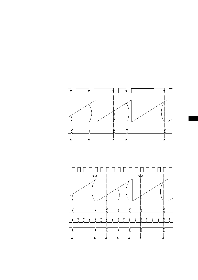
11-21
11
11
MSM66591/ML66592 User's Manual
Chapter 11 Flexible Timer (FTM)
a
b
c
d
e
a
b
c
d
e
Interrupt
request is
generated
Interrupt
request is
generated
Interrupt
request is
generated
Interrupt
request is
generated
Interrupt
request is
generated
CAPn input (fall, 1/1 dividing)
OVF
Content of counters (TM0, TM1)
0H
Content of TMRn
0
1
2
3
0
1
0
1
0
1
0
1
0
1
2
3
0
1
3
3
1
1
1
1
3
a
b
c
d
e
f
g
a
b
c
d
e
f
g
CAPn input (rise)
OVF
Content of counters (TM0, TM1)
0H
Content of TMRn
Content of EVDVn
Content of EVDVnBF
1/4 dividing
1/2 dividing
1/4 dividing
Interrupt
request is
generated
Interrupt
request is
generated
Interrupt
request is
generated
Interrupt
request is
generated
Interrupt
request is
generated
Interrupt
request is
generated
Interrupt
request is
generated
11.4.2 Operation of Type A2 Register Modules (TMR14, TMR15)
If the valid edge specified by CAPCON is input to CAP14 or CAP15 pin when the TM
specified by TMSEL is in RUN status, the divider divides the pulse in the dividing ratio
specified by EVNTCON2. In that case, an interrupt request by a capture event is
generated, and at the same time, the content of the counter specified by TMSEL is
loaded to TMRn. Also the content of the dividing counter in the divider is loaded to
buffer register EVDVnBF, and the content of the dividing counter EVDVn is cleared to
"0". Input a capture event at the interval of 3 CLKs or more. (Capture operation may be
performed only once even if the capture event is input twice or more at an interval of
less than 3 CLKs.)
Figure 11-19 (a) and (b) shows capture operation timing examples.
Figure 11-19 (a) Capture Operation Timing Example
Figure 11-19 (b) Capture Operation Timing Example

11-22
MSM66591/ML66592 User's Manual
Chapter 11 Flexible Timer (FTM)
Type A2 register modules have no "function to check a cycle of the timer counter
between capture events," which is used for the capture function of type D and E register
modules.
11.4.3 Capture Pin Dividing Circuit
The MSM66591/ML66592 type A2 timer register modules have a capture pin dividing
circuit that can perform division from 1/1 to 1/64.
[1]
Configuration of Dividing Circuit
The dividing circuit consists of the following:
∑ counter to divide valid pulses input to capture pin (EVDVn) (n = 14, 15)
∑ register to set dividing ratio (EVNTCON2)
∑ comparison circuit to compare counter value and register value
∑ register to hold dividing counter value when an event is generated (EVDVnBF) (n =
14, 15)
[2]
Operation of Dividing Circuit
If valid edges (pulses) are input to a capture pin, EVDVn counts their number. If the
counter value and the dividing value specified by EVNTCON2 match, a capture event is
generated.
If a capture event is generated, a capture interrupt request is generated, the counter
value is loaded to the timer register, the EVDVn value is loaded to EVDVnBF, and
EVDVn is cleared to "0". (n = 14, 15)
[3]
Operation to Switch Dividing Ratio
Since the dividing ratio is programmable, the dividing operation may differ, depending
on the timing that changes the dividing ratio. In this case, the MSM66591/ML66592
operate as follows:
1) When the dividing ratio is changed from 1/N to 1/M (N > M), if the valid edge is input
to a capture pin when:
∑ counter value C in the dividing circuit is C
M ≠ 1 (except when M = 1)
or
∑ M = 1
a capture event is generated.
If a valid edge is input to the capture pin when:
∑ counter value C in the dividing circuit is C < M ≠ 1 (except when M = 1)
a capture event is not generated, and the counter value in the dividing circuit is
incremented.
2) When the dividing ratio is changed from 1/N to 1/M (N < M), the dividing operation
continues until the counter value becomes M, and a capture event is generated
when the counter value becomes M.
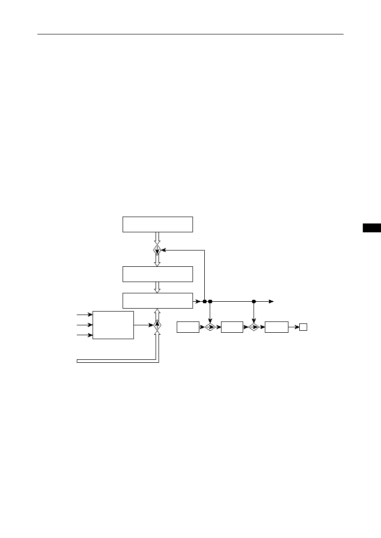
11-23
11
11
MSM66591/ML66592 User's Manual
Chapter 11 Flexible Timer (FTM)
11.5 Type B Register Modules (TMR4≠TMR13)
The MSM66591/ML66592 have 10 sets of register modules type B (TMR4≠TMR13).
The configuration is the same for these 10 sets, except for the address of registers on
SFR.
11.5.1 Configuration of Type B Register Modules (TMR4≠TMR13)
Type B register modules have a double-buffer real-time output function.
Type B register modules consist of 16-bit timer registers (TMR4≠TMR13, TMR4BF≠
TMR13BF), pins to output signals by the real-time output function (RTO4≠RTO13), a
timing controller, a comparator to compare timer counter and timer register values, and
control registers (RTOCON4≠RTOCON13), to control real-time output operations.
If RTO4≠RTO13 pins are used for real-time output functions, set the corresponding bit
of the Port 2 and Port 10 secondary function control registers to "1".
Figure 11-20 shows the configuration of a type B register module.
TMRn
CLK
TnSEL
TMDS
TMD
TMRnBF
Timing
Controller n
Comparison Circuit
Interrupt request
TnBF1
TnBF0
TnOUT
RTOn
=
n = 4≠13
Figure 11-20 Configuration of Type B Register Module

11-24
MSM66591/ML66592 User's Manual
Chapter 11 Flexible Timer (FTM)
[1]
Timer Registers (TMR4≠TMR13)
A timer register (TMR4≠TMR13) consists of 16 bits. TMR4≠TMR13 are constantly
compared with the counter values specified by TMSEL, and if they match, the contents
of TMR4BF, TMR13BF are loaded to the timer registers.
TMR4≠TMR13 can be read/written by the program.
At reset (when the
RES
signal is input, the BRK instruction is executed, the watchdog
timer is overflown, or an operation code trap is generated), TMR4≠TMR13 become
0000H.
[2]
Timer Register Buffer Registers (TMR4BF≠TMR13BF)
A timer register buffer register (TMR4BF≠TMR13BF) consists of 16 bits. If TMR4≠
TMR13 and the counter values specified by TMSEL match, the contents of TMR4BF≠
TMR13BF are loaded to TMR4≠TMR13.
TMR4BF≠TMR13BF can be read/written by the program.
At reset (when the
RES
signal is input, the BRK instruction is executed, the watchdog
timer is overflown, or an operation code trap is generated), TMR4BF≠TMR13BF
become 0000H.
[3]
Real-time Output Control Registers (RTOCON4≠RTOCON13)
A real-time output control register (RTOCON4≠RTOCON13) consists of 3 bits. If TMR4
≠TMR13 and the counter values specified by TMSEL match, the content of TnBF0 (bit
1) is loaded to TnOUT (bit 0), and the content of TnBF1 (bit 2) is loaded to TnBF0 (bit
1).
Set, to TnBF0, the level for changing for the next event and set, to TnBF1, for changing
for the event after the next.
RTOCON4≠RTOCON13 can be read/written by the program. However, writing to the
high-order 5 bits is invalid. "1s" are always read from the high-order 5 bits when read. If
a read-modify-write instruction, such as SB, RB and XORB, is executed to RTOCON4≠
RTOCON13 just before the event generated by RTO, TnBF0 and TnOUT may not
operate normally. (n = 4≠13)
At reset (when the
RES
signal is input, the BRK instruction is executed, the watchdog
timer is overflown, and an operation code trap is generated), RTOCON4≠RTOCON13
become F8H.
Figure 11-21 shows the configuration of RTOCON4≠RTOCON13.
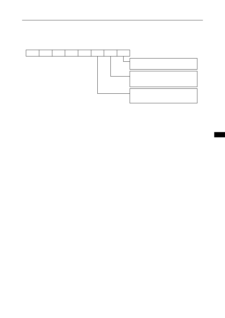
11-25
11
11
MSM66591/ML66592 User's Manual
Chapter 11 Flexible Timer (FTM)
Figure 11-21 Configuration of RTOCON4≠RTOCON13
--
--
--
--
--
TnBF1 TnBF0 TnOUT
7
6
5
4
3
2
1
0
The content of this flag is output to
an RTOn pin.
If the selected counter value and
the TMRn value match, the content
of this flag is loaded to TnOUT.
If the selected counter value and
the TMRn value match, the content
of this flag is loaded to TnBF0.
"--" indicates a bit that is not provided.
"1" is read if a read instruction is executed.
n = 4≠13
RTOCON4≠RTOCON13
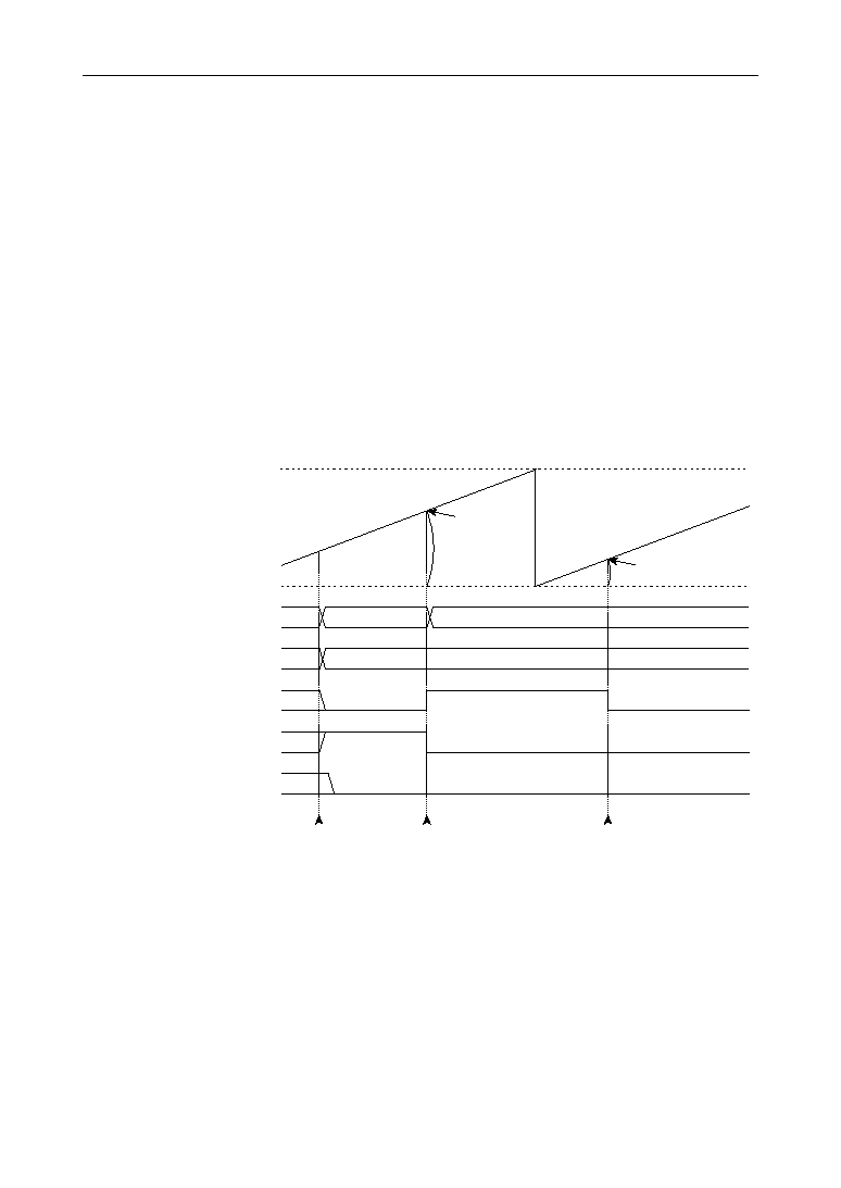
11-26
MSM66591/ML66592 User's Manual
Chapter 11 Flexible Timer (FTM)
11.5.2 Operation of Type B Register Modules (TMR4≠TMR13)
Type B register modules have a double-buffer real-time output function. When the TM
specified by TMSEL is in RUN status, TMR4≠TMR13 are constantly compared with the
specified counter value, and if they match, an interrupt request by real-time output is
generated, and the content of TMR4BF≠TMR13BF are loaded to TMR4≠TMR13. Also
the content of TnBF0 (bit 1) of RTOCON4≠RTOCON13 is loaded to TnOUT (bit 0), and
the content of TnBF1 (bit 2) is loaded to TnBF0 (bit 1). (n = 4≠13)
Therefore set the time for the next event to TMR4≠TMR13, and set the time for the
event after the next event to TMR4BF≠TMR13BF. Set the state for the next event to
TnBF0, and set the state for the event after the next event to TnBF1. Then a one-shot
pulse output can be controlled at one time.
Figure 11-22 shows a type B register module operation example.
If RTO4≠RTO13 pins are used for real-time output functions, set the corresponding bit
of the Port 2 and Port 10 secondary function control registers to "1".
Figure 11-22 Type B Register Module Operation Example
Write to
registers
Content of counters (TM0, TM1)
b
a
b
b
a
TMRn = TM
TMRn = TM
Content of TMRn
Content of TMRnBF
Content of TnOUT (RTOn)
Content of TnBF0
Content of TnBF1
Interrupt
request is
generated
Interrupt
request is
generated

11-27
11
11
MSM66591/ML66592 User's Manual
Chapter 11 Flexible Timer (FTM)
11.6 Type D Register Module (TMR17)
The MSM66591/ML66592 have one set of type D register module (TMR17).
11.6.1 Configuration of Type D Register Module (TMR17)
Type D register module has three types of functions: 4-port output RTO, RTO, and 16-
bit capture input.
Type D register module consists of 16-bit timer registers (TMR17), I/O pins (FTM17A≠
FTM17D) to either input capture signals or output signals by the real-time output
function, a timing controller, a comparison circuit to compare timer counter and timer
register values, a control register (TMRMODE) to specify the operation of the type D
register module, and control registers (RTOCON17, RTO4CON, CAPCON) to control
the operation of the type D register module.
Figure 11-23 shows the configuration of a type D register module.
If FTM17A≠FTM17D pins are used for real-time output or for capture functions, set
the corresponding bit of the Port 3 secondary function control register to "1".
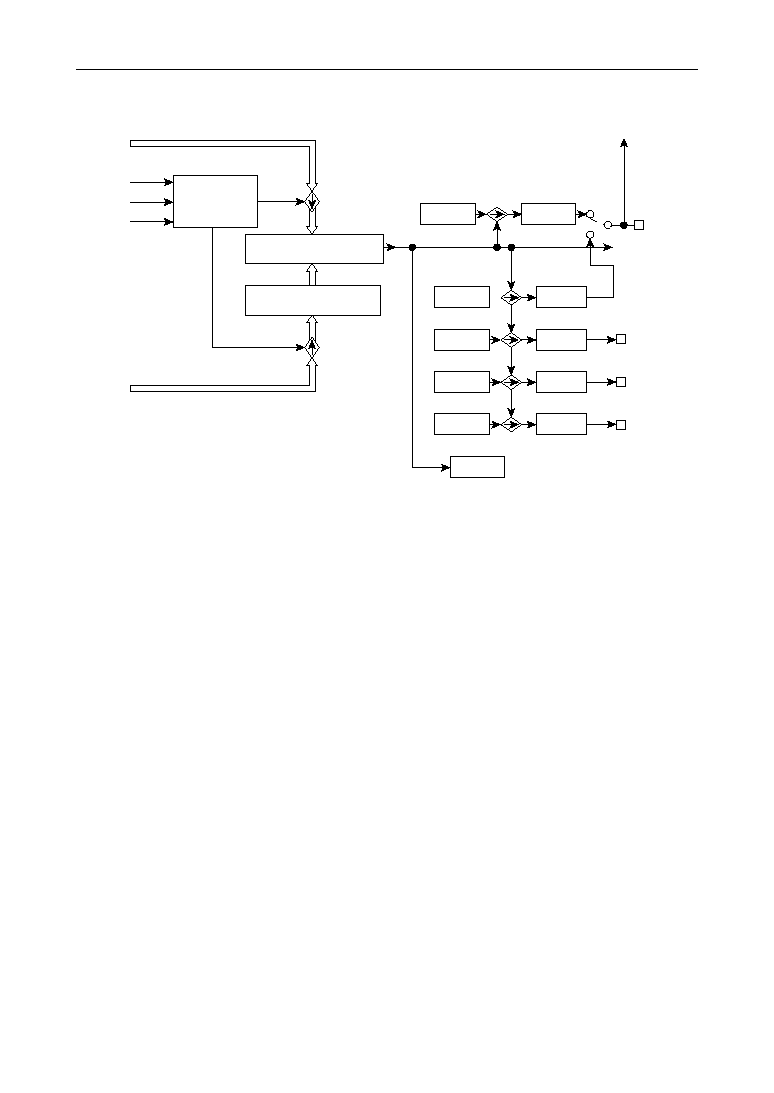
11-28
MSM66591/ML66592 User's Manual
Chapter 11 Flexible Timer (FTM)
TMD
T17BF0
FTM17B
Timing
Controller 17
CLK
T17SEL
TMDS
=
Comparison Circuit
TMR17
T17OUT
Interrupt
request
T17CER
TMD
CAP17
T17BFA
T17OUTA
T17BFB
T17OUTB
T17BFD
T17OUTD
T17BFC
T17OUTC
FTM17C
FTM17D
CAP17
FTM17A
Figure 11-23 Configuration of Type D Register Module

11-29
11
11
MSM66591/ML66592 User's Manual
Chapter 11 Flexible Timer (FTM)
[1]
Timer Register (TMR17)
A timer register consists of 16 bits (TMR17). In the case of RTO operation, TMR17 is
constantly compared with the counter value specified by TMSEL2. In the case of CAP
operation, the counter value specified by TMSEL2 is loaded when a pin event is
generated.
TMR17 can be read/written by the program. At reset (when the
RES
signal is input, the
BRK instruction is executed, the watchdog timer is overflown, and an operation code
trap is generated), TMR17 becomes 0000H.
[2]
Real-time Output Control Registers (RTOCON17, RTO4CON)
A real-time output control register (RTOCON17) consists of 3 bits. When TMR17 is in
RTO mode, if TMR17 matches the counter value specified by TMSEL2, the content of
TnBF0 (bit 1) is loaded to TnOUT (bit 0). Set the state for the next event to TnBF0.
4-port real-time output register (RTO4CON) consists of 8 bits. When TMR17 is in 4-port
RTO mode, if TMR17 matches the counter value specified by TMSEL2, the content of
T17BFA (bit 4)≠T17BFD (bit 7) is loaded to T17OUTA (bit 0)≠T17OUTD (bit 3). Set the
state for the next event to T17BFA≠T17BFD.
RTOCON17 and RTO4CON can be read/written by the program. Write to RTOCON17
is valid, however write to high-order 5 bits is invalid. Read is valid, however "1" is
always read from the high-order 5 bits. If a read-modify-write instruction such as SB,
RB, and XORB is executed to RTOCON17 or RTO4CON just prior to an event gener-
ated by RTO, TnBF0, TnOUT, T17BFA≠T17BFD, and T17OUTA≠T17OUTD may not
operate normally.
At reset (when the
RES
signal is input, the BRK instruction is executed, the watchdog
timer is overflown, or an operation code trap is generated), RTOCON17 becomes F8H,
and RTO4CON becomes 00H.
Figure 11-24 shows the configuration of RTOCON17. Figure 11-25 shows the configu-
ration of RTO4CON.
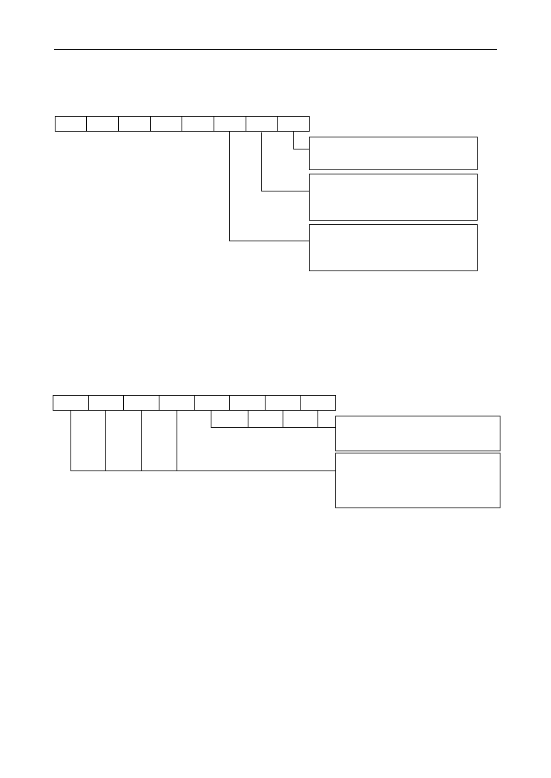
11-30
MSM66591/ML66592 User's Manual
Chapter 11 Flexible Timer (FTM)
Figure 11-24 Configuration of RTOCON17
Figure 11-25 Configuration of RTO4CON
--
--
--
--
--
T17CER T17BF0 T17OUT
7
6
5
4
3
2
1
0
When TMR17 is in RTO mode, the
content of this flag is output to a
FTM17 pin.
When TMR17 is in RTO mode, if the
selected counter value and the TMR17
value match, the content of this
flag is loaded to T17OUT.
When TMR17 is in CAP mode, if the
selected counter completes one
cycle during a capture event, the
content of this flag is "1", if not, "0".
"--" indicates a bit that is not provided.
"1" is read if a read instruction is executed.
RTOCON17
T17BFD T17BFC T17BFB T17BFA T17OUTD T17OUTC T17OUTB T17OUTA
7
6
5
4
3
2
1
0
When TMR17 is in 4-port RTO mode,
the content of this flag is output to
FTM17D≠FTM17A (pin).
When TMR17 is in 4-port RTO mode,
if the selected counter value and the
TMR17 value match, the content of
this flag is loaded to T17OUTD≠
T17OUTA.
RTO4CON
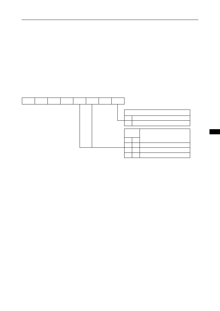
11-31
11
11
MSM66591/ML66592 User's Manual
Chapter 11 Flexible Timer (FTM)
[3]
TMR Mode Register (TMRMODE)
TMR mode register (TMRMODE) consists of 3 bits. TMRMODE sets the operational
functions of TMR16 and TMR17. TMRMODE can be read/written by the program.
At reset (when the
RES
signal is input, the BRK instruction is executed, the watchdog
timer is overflown, or an operation code trap is generated), TMRMODE becomes F2H,
TMR16 is specified to RTO mode, and TMR17 is specified to 4-port output RTO mode.
Figure 11-26 shows the configuration of TMRMODE.
7
6
5
4
3
2
1
0
--
T17MD1
--
--
--
T17MD0
--
T16MD0
TMR16 Function
0
1
RTO mode
CAP mode
T17MD
TMR17 Function
1
0
0
0
0
1
1
*
4-port RTO mode
CAP mode
RTO mode
"--" indicates a bit that is not provided.
"1" is read if a read instruction is executed.
"*" indicates either "1" or "0".
TMRMODE
Figure 11-26 Configuration of TMRMODE
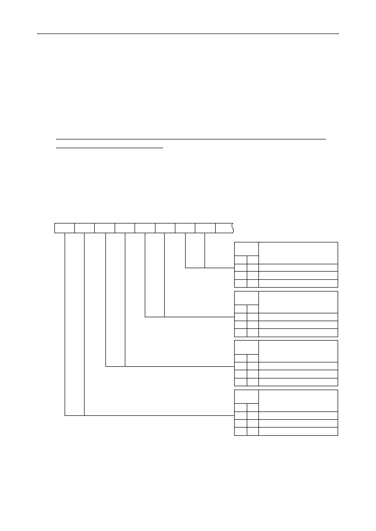
11-32
MSM66591/ML66592 User's Manual
Chapter 11 Flexible Timer (FTM)
[4]
Capture Control Register (CAPCON)
CAPCON is a 16-bit register that specifies the valid edge of a signal that is input to the
CAP0 (P3_4)≠CAP3 (P3_7) pins, CAP14 (P10_2), CAP15 (P10_3), and, when TMR16
and TMR17 are in CAP mode, to FTM16 (P10_4) and FTM17A (P3_0) pins. Bits 8≠15
of CAPCON are used to specify the valid edge of a signal to be input to CAP14
(P10_2), CAP15 (P10_3), FTM16 (P10_4), and FTM17A (P3_0) pins.
CAPCON can be read/written by the program.
Note that bit manipulation instructions such as SB and RB cannot be used, because
CAPCON has only 16-bit access.
At reset (when the
RES
signal is input, the BRK instruction is executed, the watchdog
timer is overflown, or an operation code trap is generated), CAPCON becomes 0000H,
and CAP0≠CAP3, CAP14, CAP15, TMR16, and TMR17A are specified to falling edge.
Figure 11-27 shows the configuration of bits 8≠15 of CAPCON.
Figure 11-27 Configuration of Bits 8≠15 of CAPCON
14
13
12
11
10
9
8
7
Bit
Valid edge of CAP14
1
0
0
*
1
0
1
1
Falling edge
Both edges
Rising edge
Bit
Valid edge of CAP15
3
2
0
*
1
0
1
1
Falling edge
Both edges
Rising edge
Bit
Valid edge of FTM16
(when in CAP mode)
5
4
0
*
1
0
1
1
Falling edge
Both edges
Rising edge
Bit
Valid edge of FTM17
(when in CAP mode)
7
6
0
*
1
0
1
1
Falling edge
Both edges
Rising edge
15
CAPCON (bits 8≠15)
"*" indicates either "1" or "0".
11-33
11
11
MSM66591/ML66592 User's Manual
Chapter 11 Flexible Timer (FTM)
11.6.2 Operation of Type D Register Module (TMR17)
Three functions can be selected for a type D register module by TMRMODE.
∑ real-time output mode (RTO)
∑ 4-port real-time output mode (4-port RTO)
∑ 16-bit capture register mode (CAP)
[1]
Operation in Real-time Output Mode (RTO)
When the TM specified by TMSEL2 is in RUN status, TMR17 is constantly compared
with the specified counter value, and if they match, an interrupt request by a real-time
output is generated, and the contents of T17BF0 (bit 1) of RTOCON17 are loaded to
T17OUT (bit 0).
Therefore set, to TMR17, the time for the next event and set, to T17BF0, the state for
the next event. The RTO4CON function becomes invalid.
Figure 11-28 shows an example of a type D register module operation in RTO mode.
If FTM17A pin is used as RTO function, the bit corresponding to the Port-3 secondary
function control register must be set to "1". In this case RTO4CON becomes invalid.
Figure 11-28 Example of Type D Register Module Operation in RTO Mode
Content of counters (TM0, TM1)
c
a
c
a
TMR17 = TM
Content of TMR17
Content of T17OUT (RTO17)
Content of T17BF0
TMR17 = TM
b
d
b
d
Write to
registers
Interrupt request
is generated
Write to TMR17,
T17BF0
Interrupt request
is generated
Write to TMR17
Interrupt request is generated
Write to TMR17,
T17BF0
Interrupt request
is generated
Write to TMR17
11-34
MSM66591/ML66592 User's Manual
Chapter 11 Flexible Timer (FTM)
Figure 11-29 Example of Type D Register Module Operation in 4-Port RTO Mode
T17OUTB (FTM17B)
Content of counters (TM0, TM1)
c
a
c
a
TMR17 = TM
Content of TMR17
T17OUTA (FTM17A)
TMR17 = TM
b
d
b
d
T17OUTC (FTM17C)
T17OUTD (FTM17D)
T17BFA
T17BFB
T17BFC
T17BFD
Write to
registers
Interrupt request
is generated
Write to TMR17,
T17BFA≠T17BFD
Interrupt request
is generated
Write to TMR17,
T17BFA≠T17BFD
Interrupt request
is generated
Write to TMR17,
T17BFA≠T17BFD
Interrupt request
is generated
Write to TMR17,
T17BFA≠T17BFD
[2]
Operation in 4-Port Output Real-time Output Mode (4-Port RTO)
When the TM specified by TMSEL2 is in RUN status, TMR17 is constantly compared
with the specified counter value, and if they match, an interrupt request by a real-time
output is generated, and the contents of T17BFA≠T17BFD (bits 4≠7) of RTO4CON are
loaded to T17OUTA≠T17OUTD (bits 0≠3).
Figure 11-29 shows an example of a register module type D operation in 4-port RTO
mode.
If FTM17A≠FTM17D pins are used as 4-port RTO function, the bit corresponding to the
Port-3 secondary function control register must be set to "1". In this case RTOCON7
becomes invalid.
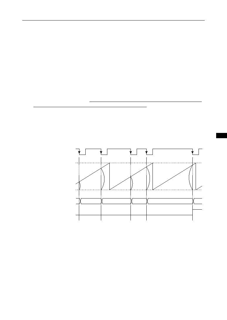
11-35
11
11
MSM66591/ML66592 User's Manual
Chapter 11 Flexible Timer (FTM)
[3]
Operation in CAP Mode
When the TM specified by TMSEL2 is in RUN status, if the valid edge specified by
CAPCON is input to FTM17A pin, an interrupt request by a capture event is generated,
and at the same time, the content counter specified by TMSEL2 is loaded to TMR17.
Flag T17CER is provided in the register module type D. This flag checks whether the
cycle of the selected counter between capture events is completed or not. If the
counter cycle is completed since the last capture event generation (contents of
TMR17), T17CER (bit 2) of RTOCON17 is set to "1" if the capture value is more than or
equal to the "last capture value +1". This bit remains at "0" if the cycle is not completed
(when the capture value is less than or equal to the last capture value).
The cycle flag is set to "1" at the timing of the next capture operation after the above
mentioned condition is met. Note that when capture operations are not performed, the
cycle flag is not set even if the counter cycle is completed.
Figure 11-30 shows a capture operation timing example.
If FTM17A pin is used for CAP functions, set the corresponding bit of the Port 3 sec-
ondary function control registers to "1". When in CAP mode, RTOCON17 and
RTO4CON are invalid.
Figure 11-30 Example of Type D Register Module Operation in CAP Mode
a
b
c
d
e
a
b
c
d
e
v
v
v
v
v
Interrupt
request is
generated
Interrupt
request is
generated
Interrupt
request is
generated
Interrupt
request is
generated
FTM17A input
(falling edge)
OVF
Content of counters (TM0, TM1)
0H
Content of TMR17
Interrupt
request is
generated
T17CER
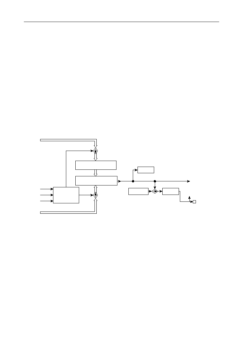
11-36
MSM66591/ML66592 User's Manual
Chapter 11 Flexible Timer (FTM)
11.7 Type E Register Module (TMR16)
The MSM66591/ML66592 have one set of type E register module (TMR16).
11.7.1 Configuration of Type E Register Module (TMR16)
Type E register module has two types of functions: RTO and 16-bit capture input.
Type E register module consists of 16-bit timer register (TMR16), I/O pins (FTM16) to
either input capture signals or output signals by the real-time output function, a timing
controller, a comparison circuit to compare timer counter and timer register values, a
control register (TMRMODE) to specify the operation of a type E register module, and
control registers (RTOCON16, CAPCON) to control the operation of the type E register
module.
Figure 11-31 shows the configuration of a register module type E.
If FTM16 pin is used for real-time output or for capture functions, set the correspond-
ing bit of the Port 10 secondary function control register to "1".
TMR16
Timing
Controller 16
TMD
Comparsion Circuit
CLK
T16SEL
TMDS
=
T16OUT
Interrupt request
T16BF0
FTM16
T16CER
TMD
CAP16
CAP16
Figure 11-31 Configuration of Type E Register Module
11-37
11
11
MSM66591/ML66592 User's Manual
Chapter 11 Flexible Timer (FTM)
[1]
Timer Register (TMR16)
A timer register consists of 16 bits (TMR16). In the case of RTO operation, TMR16 is
constantly compared with the counter value specified by TMSEL2. In the case of CAP
mode, the counter value specified by TMSEL2 is loaded to the timer register when a pin
event is generated.
TMR16 can be read/written by the program. At reset (when the
RES
signal is input, the
BRK instruction is executed, the watchdog timer is overflown, or an operation code trap
is generated), TMR16 becomes 0000H.
[2]
Real-time Output Control Register (RTOCON16)
A real-time output control register (RTOCON16) consists of 3 bits. When TMR16 is in
RTO mode, if TMR16 matches the counter value specified by TMSEL2, the content of
T16BF0 (bit 1) is loaded to T16OUT (bit 0). Set the state for the next event to T16BF0.
RTOCON16 can be read/written by the program. Write is valid, however write to high-
order 5 bits is invalid. Read is valid, however "1" is always read from the high-order 5
bits. If a read-modify-write instruction, such as SB, RB, and XORB, is executed to
RTOCON16 just prior to an event generated by RTO, T16BF0 and T16OUT may not
operate normally.
At reset (when the
RES
signal is input, the BRK instruction is executed, the watchdog
timer is overflown, or an operation code trap is generated), RTOCON16 becomes F8H.
Figure 11-32 shows the configuration of RTOCON16.
Figure 11-32 Configuration of RTOCON16
--
--
--
--
--
T16CER T16BF0 T16OUT
7
6
5
4
3
2
1
0
When TMR16 is in RTO mode, the
content of this flag is output to a
FTM16 pin.
When TMR16 is in RTO mode, if the
selected counter value and the TMR16
value match, the content of this flag
is loaded to T16OUT.
When TMR16 is in CAP mode, if the
selected counter completes one
cycle during a capture event, the
content of this flag is "1", if not, "0".
"--" indicates a bit that is not provided.
"1" is read if a read instruction is executed.
RTOCON16
11-38
MSM66591/ML66592 User's Manual
Chapter 11 Flexible Timer (FTM)
[3]
TMR Mode Register (TMRMODE)
TMR mode register (TMRMODE) consists of 3 bits. TMRMODE sets the operational
functions of TMR16 and TMR17. TMRMODE can be read/written by the program.
At reset (when the
RES
signal is input, the BRK instruction is executed, the watchdog
timer is overflown, or an operation code trap is generated), TMRMODE becomes F2H,
TMR16 is specified to RTO mode, and TMR17 is specified to 4-port output RTO mode.
Figure 11-33 shows the configuration of TMRMODE.
7
6
5
4
3
2
1
0
--
T17MD1
--
--
--
T17MD0
--
T16MD0
Function of TMR16
0
1
RTO mode
CAP mode
T17MD
Function of TMR17
1
0
0
0
0
1
1
*
4-port RTO mode
CAP mode
RTO mode
"--" indicates a bit that is not provided.
"1" is read if a read instruction is executed.
"*" indicates either "1" or "0".
TMRMODE
Figure 11-33 Configuration of TMRMODE

11-39
11
11
MSM66591/ML66592 User's Manual
Chapter 11 Flexible Timer (FTM)
[4]
Capture Control Register (CAPCON)
CAPCON is a 16-bit register that specifies the valid edge of a signal that is input to the
CAP0 (P3_4)≠CAP3 (P3_7) pins, CAP14 (P10_2), CAP15 (P10_3), and, when TMR16
and TMR17 are in CAP mode, to FTM16 (P10_4) and FTM17A (P3_0) pins. Bits 8≠15
of CAPCON are used to specify the valid edge of a signal to be input to CAP14
(P10_2), CAP15 (P10_3), FTM16 (P10_4), and FTM17A (P3_0) pins.
CAPCON can be read/written by the program.
Note that bit manipulation instructions such as SB and RB cannot be used, because
CAPCON has only 16-bit access.
At reset (when the
RES
signal is input, the BRK instruction is executed, the watchdog
timer is overflown, or an operation code trap is generated), CAPCON becomes 0000H,
and CAP0≠CAP3, CAP14, CAP15, TMR16, and TMR17A are specified to falling edge.
Figure 11-34 shows the configuration of bits 8≠15 of CAPCON.
Figure 11-34 Configuration of Bits 8≠15 of CAPCON
15
14
13
12
11
10
9
8
Bit
Valid edge of CAP14
1
0
0
*
1
0
1
1
Falling edge
Both edges
Rising edge
Bit
Valid edge of CAP15
3
2
0
*
1
0
1
1
Falling edge
Both edges
Rising edge
7
Bit
Valid edge of FTM16
(CAP mode)
5
4
0
*
1
0
1
1
Falling edge
Both edges
Rising edge
Bit
Valid edge of FTM17
(CAP mode)
7
6
0
*
1
0
1
1
Falling edge
"*" indicates either "1" or "0".
Both edges
Rising edge
CAPCON (bits 8≠15)

11-40
MSM66591/ML66592 User's Manual
Chapter 11 Flexible Timer (FTM)
11.7.2 Operation of Type E Register Module (TMR16)
Two functions can be selected for a type E register module by TMRMODE.
∑ real-time output mode (RTO)
∑ 16-bit capture mode (CAP)
[1]
Operation in Real-time Output Mode (RTO)
When the TM specified by TMSEL2 is in RUN status, TMR16 is constantly compared
with the specified counter value, and if they match, an interrupt request by a real-time
output is generated, and the contents of T16BF0 (bit 1) of RTOCON16 are loaded to
T16OUT (bit 0).
Therefore set the time for the next event to TMR16 and set the state for the next event
to T16BF0.
Operation in RTO mode of a type E register module is the same as the RTO mode of a
register module type D. (See Figure 11-28.)
If FTM16 pin is used for RTO functions, set the corresponding bit of the Port 10 second-
ary function control register to "1".
[2]
Operation in CAP Mode
When the TM specified by TMSEL2 is in RUN status, if the valid edge specified by
CAPCON is input to FTM16 pin, an interrupt request by a capture event is generated,
and at the same time, the content counter specified by TMSEL2 is loaded to TMR16. If
the counter cycle is completed (= if the register value and the counter value match)
since the last capture event generation (contents of TMR16), T16CER (bit 2) of
RTOCON16 is set to "1". It remains at "0" if the cycle is not completed.
The operation in CAP mode of type E register module is the same as that in CAP mode
of type D register module. (See Figure 11-30.)
If FTM16 pin is used for CAP mode, set the corresponding bit of the Port 10 secondary
function control register to "1". When in CAP mode, RTOCON16 is invalid.

11-41
11
11
MSM66591/ML66592 User's Manual
Chapter 11 Flexible Timer (FTM)
11.8 RTO Mode Output Timing Changes
Figure 11-35 shows an example of RTO mode output timing changes of register
modules type B, type D, and type E.
Figure 11-35 uses the RTO output function of type B register module as an example.
TM1 is incremented every 1/5 CLK. When the content of TMRn is 100H, the match
signal of TM1 and TMRn becomes H level while the content of TM1 is 100H. TMRn and
the RTO output pin change at the fall of the match signal, and by the AND signal of the
TM1 clock pulse. The corresponding interrupt request flag is set at the latter half of
M1S1 (signal to indicate the beginning of an instruction).
Figure 11-35 Example of Type B Register Module Output Timing Changes
100H
101H
102H
100H
Clock of TM1 1/5 CLK
Master clock (CLK)
Content of TM1
Match signal
of TM1 and TMRn
M1S1
Change of TMRn content
and RTO output pin, etc.
IRQ
Interrupt transition cycle
(MIE, IE = "1")

11-42
MSM66591/ML66592 User's Manual
Chapter 11 Flexible Timer (FTM)

General-Purpose 8-Bit Timer
Function
Chapter 12
12

12-1
MSM66591/ML66592 User's Manual
Chapter 12 General-Purpose 8-Bit Timer Function
12
12. General-Purpose 8-Bit Timer Function
The MSM66591/ML66592 have one general-purpose 8-bit timer (GTM) and one
general-purpose 8-bit event counter (GEVC).
Table 12-1 lists the GTM control SFRs.
Table 12-1 GTM Control SFRs
Address[H]
Name
Abbreviated
Name (BYTE)
R/W
8/16-Bit
Operation
8
Reset
State [H]
016A
General-Purpose 8-Bit Timer Control Register
GTMCON
30
016B
General-Purpose 8-Bit Event Counter
GEVC
00
016C
General-Purpose 8-Bit Timer Counter
GTMC
00
016D
General-Purpose 8-Bit Timer Register
GTMR
00
Abbreviated
Name (WORD)
Addresses in the address column marked by "" indicate that the register has bits missing.
R/W
--
--
--
--
004E
GTINTCON
F0
--
General-Purpose 8-Bit Timer
Interrupt Control Register

12-2
MSM66591/ML66592 User's Manual
Chapter 12 General-Purpose 8-Bit Timer Function
1/2 TBCCLK
1/4 TBCCLK
1/8 TBCCLK
1/16 TBCCLK
1/64 TBCCLK
1/256 TBCCLK
External rise
External fall
GTMC
GTMR
Interrupt
request
GTMCON
OVF
Selector
QGTM
EGTM
Figure 12-1 Configuration of GTM
[Note]
When the general purpose 8-bit timer, used in external clock mode, is switched to
STOP mode, and when STOP mode is cleared by an interrupt, the 8-bit timer counter
(GTMC) may be incremented by 1 depending on the input level of the external clock
(P9_6/ETMCK pin) at that time.
12.1 General-Purpose 8-Bit Timer (GTM)
The general-purpose 8-bit timer consists of an 8-bit timer counter (GTMC), an 8-bit
timer register (GTMR) that stores the reload values of GTMC, and a general-purpose 8-
bit timer control register (GTMCON) that controls operations. Figure 12-1 shows the
configuration of GTM.
General-purpose 8-bit timer interrupts and general-purpose 8-bit event counter inter-
rupts are assigned to the same interrupt vector. Indication of whether each individual
interrupt request has been generated or not and whether to enable or disable genera-
tion of each individual interrupt request are specified by the general-purpose 8-bit timer
interrupt control register (GTINTCON).

12-3
MSM66591/ML66592 User's Manual
Chapter 12 General-Purpose 8-Bit Timer Function
12
[1]
General-Purpose 8-Bit Timer Counter (GTMC)
The GTMC is an 8-bit counter that generates an interrupt request when an overflow
occurs, and at the same time, the content of the general-purpose 8-bit timer register
(GTMR) is loaded. The count clock of GTMC is selected by the low-order 3 bits of the
general-purpose 8-bit timer control register (GTMCON).
At reset (when the
RES
signal is input, the BRK instruction is executed, the watchdog
timer is overflown, or an operation code trap is generated), GTMC becomes 00H, and
the count operation stops. In STOP mode and if external clock (P9_6/ETMCK pin) is
specified as the counter clock of GTMC, GTMC counts at the falling edge of the count
clock.
[2]
General-Purpose 8-Bit Timer Register (GTMR)
GTMR is an 8-bit register, and its content is loaded to GTMC when a GTMC overflow
occurs. At reset (when the
RES
signal is input, the BRK instruction is executed, the
watchdog timer is overflown, or an operation code trap is generated), GTMR becomes
00H.
[3]
General-Purpose 8-Bit Timer Control Register (GTMCON)
GTMCON is an 8-bit register that selects the count clock of GTMC and controls the
start/stop of the count operation using the low-order 4 bits. It also selects the count
clock of GEVC and controls the start/stop of the count operation using the high-order 2
bits.
If external clock is seleced as the counter clock of GTMC, GTMC counts inputs to the
P9_6/ETMCLK pin.
At reset (when the
RES
signal is input, the BRK instruction is executed, the watchdog
timer is overflown, or an operation code trap is generated), GTMCON becomes 30H, a
1/2 TBCCLK is selected as the count clock of GTMC, and the count operation stops.
The external clock rising edge is selected as the count clock of GEVC, and the count
operation stops.
Figure 12-2 shows the configuration of GTMCON.

12-4
MSM66591/ML66592 User's Manual
Chapter 12 General-Purpose 8-Bit Timer Function
Figure 12-2 Configuration of GTMCON
GEVRUN GEVCK
--
--
GTMRUN GTMCK2 GTMCK1 GTMCK0
7
6
5
4
3
2
1
0
GTMCK
Count Clock of GTMC
2 1 0
0 0 0 1/2 TBCCLK
0 0 1 1/4 TBCCLK
0 1 0 1/8 TBCCLK
0 1 1 1/16 TBCCLK
1 0 0 1/64 TBCCLK
1 0 1 1/256 TBCCLK
1 1 0 External rise (P9_6/ETMCK pin)
1 1 1 External fall (P9_6/ETMCK pin)
0 GTMC count operation stop
1 GTMC count runs
0 GEVC count clock external rise (P9_7/ECTCK pin)
1 GEVC count clock external fall (P9_7/ECTCK pin)
0 GEVC count operation stop
1 GEVC count runs
"--" indicates a bit that is not provided.
"1" is read if a read instruction is executed.
GTMCON

12-5
MSM66591/ML66592 User's Manual
Chapter 12 General-Purpose 8-Bit Timer Function
12
[4]
General-Purpose 8-Bit Timer Interrupt Control Register (GTINTCON)
GTINTCON is an 8-bit register that controls the generation of interrupts for the general-
purpose 8-bit timer and general-purpose 8-bit event counter.
At reset (when the
RES
signal is input, the BRK instruction is executed, the watchdog
timer is overflown, or an operation code trap is generated), GTINTCON becomes F0H.
Figure 12-3 shows the configuration of GTINTCON.
[Description of Each Bit]
∑ EGTM (bit 0)
The EGTM bit enables or disables the generation of interrupt requests by the gen-
eral-purpose 8-bit timer (GTMC).
When this bit is "0", interrupts are disabled. When "1", interrupts are enabled.
∑ QGTM (bit 1)
QGTM indicates whether an interrupt request has been generated by the general-
purpose 8-bit timer (GTMC).
When this bit is "0", no interrupt request has been generated. When "1", an interrupt
request has been generated.
∑ EEVC (bit 2)
EEVC enables or disables the generation of interrupt requests by the general-
purpose 8-bit event counter (GEVC).
When this bit is "0", interrupts are disabled. When "1", interrupts are enabled.
∑ QEVC (bit 3)
QEVC indicates whether an interrupt request has been generated by the general-
purpose 8-bit event counter (GEVC).
When this bit is "0", no interrupt request has been generated. When "1", an interrupt
request has been generated.
Figure 12-3 GTINTCON Configuration
"--" indicates a bit that is not provided.
"1" is read if a read instruction is executed.
--
QEVC EEVC QGTM EGTM
1
0
GTMC interrupt request generation: enabled
GTMC interrupt request generation: disabled
1
0
GEVC interrupt request generation: enabled
GEVC interrupt request generation: disabled
1
0
GTMC interrupt request generation: yes
GTMC interrupt request generation: no
--
--
--
1
0
GEVC interrupt request generation: yes
GEVC interrupt request generation: no
7
3
2
1
0
6
5
4
GTINTCON
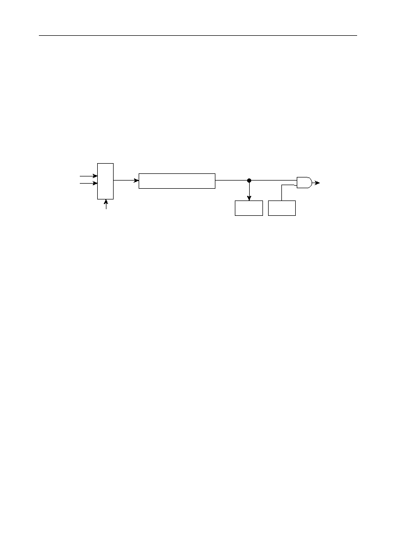
12-6
MSM66591/ML66592 User's Manual
Chapter 12 General-Purpose 8-Bit Timer Function
12.2 General-Purpose 8-Bit Event Counter (GEVC)
The general-purpose 8-bit event counter consists of an 8-bit counter (GEVC), and an 8-
bit general-purpose 8-bit timer control register (GTMCON) that controls operations.
Figure 12-4 shows the configuration of GEVC.
General-purpose 8-bit timer interrupts and general-purpose 8-bit event counter inter-
rupts are assigned to the same interrupt vector. Indication of whether each individual
interrupt request has been generated or not and whether to enable or disable genera-
tion of each individual interrupt request are specified by the general-purpose 8-bit timer
interrupt control register (GTINTCON).
Figure 12-4 Configuration of GEVC
External rise
External fall
GEVC
OVF
GTMCON
Selector
Interrupt
QEVC
EEVC
[Note]
When the general-purpose 8-bit counter is set to STOP mode, and when STOP mode is
cleared by an interrupt, the 8-bit event counter (GEVC) may be incremented by 1
depending on the input level of the external clock (P9_7/ECTCK pin) at that time.
[1]
General-Purpose 8-Bit Event Counter (GEVC)
The GEVC is an 8-bit counter that generates an interrupt request when an overflow
occurs. The count clock of the GEVC is selected by the high-order 2 bits of the general-
purpose 8-bit timer control register (GTMCON).
At reset (when the
RES
signal is input, the BRK instruction is executed, the watchdog
timer is overflown, or an operation code trap is generated), the GEVC becomes 00H,
and the count operation stops. In STOP mode, the GEVC operates at the falling edge
of the external clock.
[2]
General-Purpose 8-Bit Timer Control Register (GTMCON)
The GTMCON is an 8-bit register that counts inputs to the P9_7/ECTCK pin. It selects
the count clock of the GTMC and controls the start/stop of the count operation using the
low-order 4 bits. It also selects the count clock of the GEVC and controls the start/stop
of the count operation using the high-order 2 bits. GEVC counts inputs to the P9_7/
ECTCK pin.
At reset (when the
RES
signal is input, the BRK instruction is executed, the watchdog
timer is overflown, or an operation code trap is generated), the GTMCON becomes
30H, a 1/2 TBCCLK is selected as the count clock of the GTMC, and the count opera-
tion stops. The external clock rising edge is selected as the count clock of the GEVC,
and the count operation stops.
Figure 12-2 (page 12-4) shows the configuration of the GTMCON.

12-7
MSM66591/ML66592 User's Manual
Chapter 12 General-Purpose 8-Bit Timer Function
12
[3]
General-Purpose 8-Bit Timer Interrupt Control Register (GTINTCON)
GTINTCON is an 8-bit register that controls the generation of interrupts for the general-
purpose 8-bit timer and general-purpose 8-bit event counter.
At reset (when the
RES
signal is input, the BRK instruction is executed, the watchdog
timer is overflown, or an operation code trap is generated), GTINTCON becomes F0H.
Figure 12-3 (page 12-5) shows the configuration of GTINTCON.
[Description of Each Bit]
∑ EGTM (bit 0)
The EGTM bit enables or disables the generation of interrupt requests by the gen-
eral-purpose 8-bit timer (GTMC).
When this bit is "0", interrupts are disabled. When "1", interrupts are enabled.
∑ QGTM (bit 1)
QGTM indicates whether an interrupt request has been generated by the general-
purpose 8-bit timer (GTMC).
When this bit is "0", no interrupt request has been generated. When "1", an interrupt
request has been generated.
∑ EEVC (bit 2)
EEVC enables or disables the generation of interrupt requests by the general-
purpose 8-bit event counter (GEVC).
When this bit is "0", interrupts are disabled. When "1", interrupts are enabled.
∑ QEVC (bit 3)
QEVC indicates whether an interrupt request has been generated by the general-
purpose 8-bit event counter (GEVC).
When this bit is "0", no interrupt request has been generated. When "1", an interrupt
request has been generated.

12-8
MSM66591/ML66592 User's Manual
Chapter 12 General-Purpose 8-Bit Timer Function

PWM Functions
Chapter 13
13

13-1
13
MSM66591/ML66592 User's Manual
Chapter 13 PWM Functions
13. PWM Functions
The MSM66591/ML66592 have 12 channels of PWM functions. PWM consists of a
count clock dividing circuit, a 16-bit counter, three 16-bit registers, various control
registers, etc.
If the master clock is 24 MHz, a 10.6
m
sec (valid bit length: 8 bits) to 838.9 msec (valid
bit length: 16 bits) cycle can be selected by combining the input clock of the PWM
counter and a valid bit length.
Figure 13-1 shows the configuration of PWM. Table 13-1 lists the PWM control SFRs.
Figure 13-1 Configuration of PWM
CLK (master clock)
Interrupt
TBCCLK
PWCnBF
Comparator
PWnBF
PWRn
Active
Controller
To port
Sele-
ctor
PWCn
R
S
Q
Q
Output F/F
Interrupt
1/2 TBCCLK
1/4 TBCCLK
1/8 TBCCLK
1/16 TBCCLK
TBC
UDF
n = 0≠11
1/n
13-2
MSM66591/ML66592 User's Manual
Chapter 13 PWM Functions
Table 13-1 PWM Control SFRs
PWM Counter 0/
PWC0 Buffer Register
0050
R/W
(*1)
FFFF
0051
0053
0054
0055
0056
0057
0058
0059
005A
005B
005C
005D
005E
005F
0060
0061
0062
0063
0064
0065
0066
0067
0068
0069
006A
006B
006C
006D
006E
006F
0070
0071
0072
0073
0074
0075
0076
0077
0078
0079
007A
007B
007C
007D
007F
007E
PWM Counter 1/
PWC1 Buffer Register
PWM Counter 2/
PWC2 Buffer Register
PWM Counter 3/
PWC3 Buffer Register
PWM Counter 4/
PWC4 Buffer Register
PWM Counter 5/
PWC5 Buffer Register
PWM Counter 6/
PWC6 Buffer Register
PWM Counter 7/
PWC7 Buffer Register
PWM Counter 8/
PWC8 Buffer Register
PWM Counter 9/
PWC9 Buffer Register
PWM Counter 10/
PWC10 Buffer Register
PWM Counter 11/
PWC11 Buffer Register
PWM Register 0/
PWR0 Buffer Register
PWM Register 1/
PWR1 Buffer Register
PWM Register 2/
PWR2 Buffer Register
PWM Register 3/
PWR3 Buffer Register
PWM Register 4/
PWR4 Buffer Register
PWM Register 5/
PWR5 Buffer Register
0052
PWM Register 6/
PWR6 Buffer Register
PWM Register 7/
PWR7 Buffer Register
PWM Register 8/
PWR8 Buffer Register
PWM Register 9/
PWR9 Buffer Register
PWM Register 10/
PWR10 Buffer Register
PWM Register 11/
PWR11 Buffer Register
--
--
--
--
--
--
--
--
--
--
--
--
--
--
--
--
--
--
--
--
--
--
--
--
PWC0/
PWC0BF
PWC1/
PWC1BF
PWC2/
PWC2BF
PWC3/
PWC3BF
PWC4/
PWC4BF
PWC5/
PWC5BF
PWC6/
PWC6BF
PWC7/
PWC7BF
PWC8/
PWC8BF
PWC9/
PWC9BF
PWC10/
PWC10BF
PWC11/
PWC11BF
PWR0/
PW0BF
PWR1/
PW1BF
PWR2/
PW2BF
PWR3/
PW3BF
PWR4/
PW4BF
PWR5/
PW5BF
PWR6/
PW6BF
PWR7/
PW7BF
PWR8/
PW8BF
PWR9/
PW9BF
PWR10/
PW10BF
PWR11/
PW11BF
R/W
(*2)
16
FFFF
FFFF
FFFF
FFFF
FFFF
FFFF
FFFF
FFFF
FFFF
FFFF
FFFF
0000
0000
0000
0000
0000
0000
0000
0000
0000
0000
0000
0000
*1 The counter value is read if a read instruction is executed, and data is written to the buffer if a write
instruction is executed.
*2 The register value is read if a read instruction is executed, and data is written to the buffer if a write
instruction is executed.
Address [H]
Name
Abbreviated
Name (BYTE)
R/W
8/16-Bit
Operation
Reset
State [H]
Abbreviated
Name (WORD)
13-3
13
MSM66591/ML66592 User's Manual
Chapter 13 PWM Functions
Table 13-1 PWM Control SFRs (continued)
PWMRUN Register
0080
R/W
0081
0083
0084
0085
0086
0087
0088
0089
0160
0161
0162
0163
0164
0165
PWM Interrupt Register 0
PWM Interrupt Register 1
PWM Interrupt Enable
Register 0
PWM Interrupt Enable
Register 1
PWM Control Register 0
PWM Control Register 2
PWM Control Register 4
0082
PWRUNL
PWINTQ0L
PWINTQ1L
PWINTE0L
PWINTE1L
PWCON0
PWCON2
PWCON4
PWRUN
PWINTQ0
PWINTQ1
PWINTE0
PWINTE1
PWM Control Register 1
PWM Control Register 3
PWM Control Register 5
PWCON1
PWCON3
PWCON5
--
--
--
--
--
--
PWRUNH
PWINTQ0H
PWINTQ1H
PWINTE0H
PWINTE1H
R/W
8
8/16
00
00
00
00
00
00
00
00
00
00
00
F0
F0
F0
F0
F0
Some addresses are not consecutive.
Addresses in the address column marked by "" indicate that the register has bits missing.
Address [H]
Name
Abbreviated
Name (BYTE)
R/W
8/16-Bit
Operation
Reset
State [H]
Abbreviated
Name (WORD)

13-4
MSM66591/ML66592 User's Manual
Chapter 13 PWM Functions
13.1 Configuration of PWM
The MSM66591/ML66592 have 12 sets of PWM functions (PWM0≠PWM11). PWM0≠
PWM11 have the same configuration except for the SFR address.
PWM consists of 16-bit counters (PWC0≠PWC11), 16-bit counter buffer registers
(PWC0BF≠PWC11BF), 16-bit registers (PWR0≠PWR11), 16-bit buffer registers
(PW0BF≠PW11BF), a comparison circuit for PWC0≠PWC11 and PWR0≠PWR11, an
output F/F, and various control registers (PWINTQ0, PWINTQ1, PWINTE0, PWINTE1,
PWCON0≠PWCON5 and PWRUN) that control operations.
If PWM0≠PWM11 pins are used for PWM functions, set the corresponding bit of the
Port 7 and Port 8 secondary function control registers to "1". If the
OE
pin is in "L" level,
PWM0≠PWM11 pins operate (outputs) as a PWM function, but if the
OE
pin is in "H"
level, PWM0≠PWM11 pins go into high impedance status.
[1]
PWM Counters (PWC0≠PWC11)
PWC0≠PWC11 are 16-bit down counters. The input clock can be selected from among
the master clock, TBCCLK, 1/2 TBCCLK, 1/4 TBCCLK, 1/8 TBCCLK, and 1/16
TBCCLK. If an underflow occurs when the corresponding PWnRUN bit is "1" and
PWC0≠PWC11 are in count operations, the PWM counter generates an interrupt
request (PWC0 and PWC1, PWC2 and PWC3, PWC4 and PWC5, PWC6 and PWC7,
PWC8 and PWC9, PWC10 and PWC11 are common), and the contents of the 16-bit
PWM counter buffer register are loaded to the PWM counters. The PWM counter then
loads the content of the 16-bit PWM buffer register to the 16-bit PWM register, and sets
the output F/F to "1".
PWC0≠PWC11 can be read, but cannot be written, by the program. However, if
PWC0BF≠PWC11BF are written when the corresponding PWnRUN bit is "0" (stop
status), the 16-bit contents are written to PWC0≠PWC11 as well.
At reset (when the
RES
signal is input, the BRK instruction is executed, the watchdog
timer is overflown, or an operation code trap is generated), PWC0≠PWC11 become
FFFFH.
[2]
PWM Counter Buffer Registers (PWC0BF≠PWC11BF)
PWC0BF≠PWC11BF are 16-bit registers for setting cycles (for storing the reload values
for PWC0≠PWC11). If PWC0≠PWC11 underflow, the contents of PWC0BF≠PWC11BF
are loaded to the 16-bit PWM counter.
PWC0BF≠PWC11BF can be read, but cannot be written, by the program. If PWC0BF≠
PWC11BF are written to when the corresponding PWnRUN bit is "0" (stop status), the
contents of 16-bits are written to PWC0≠PWC11 as well.
At reset (when the
RES
signal is input, the BRK instruction is executed, the watchdog
timer is overflown, or an operation code trap is generated), PWC0BF≠PWC11BF
become FFFFH.

13-5
13
MSM66591/ML66592 User's Manual
Chapter 13 PWM Functions
[3]
PWM Registers (PWR0≠PWR11)
PWR0≠PWR11 are 16-bit registers that store the duty values to output. If PWC0≠
PWC11 underflow, the contents of the 16-bit PWM buffer register are loaded to PWR0≠
PWR11.
PWR0≠PWR11 can be read, but cannot be written, by the program. However, if the
corresponding PWnRUN bit is "0" (stop status), and PW0BF≠PW11BF are written to,
the contents of 16 bits are written to PWR0≠PWR11 as well.
At reset (when the
RES
signal is input, the BRK instruction is executed, the watchdog
timer is overflown, or an operation code trap is generated), PWR0≠PWR11 become
0000H.
[4]
PWM Buffer Registers (PW0BF≠PW11BF)
PW0BF≠PW11BF are 16-bit registers. If PWC0≠PWC11 underflow, the contents of the
PWM buffer register are loaded to the PWM register. PW0BF≠PW11BF can be written,
but cannot be read, by the program. If the corresponding PWnRUN bit is "0" (stop
status), and PW0BF≠PW11BF are written to, the contents of 16-bits are written to
PWR0≠PWR11 as well.
At reset (when the
RES
signal is input, the BRK instruction is executed, the watchdog
timer is overflown, or an operation code trap is generated), PW0BF≠PW11BF become
0000H.
[5]
Comparison Circuit
The comparison circuit constantly compares the content of PWC0≠PWC11 and that of
PWR0≠PWR11 when the corresponding PWnRUN bit is "1". It generates an interrupt
request (PWM0 and PWM1, PWM2 and PWM3, PWM4 and PWM5, PWM6 and PWM7,
PWM8 and PWM9, PWM10 and PWM11 are common) and resets the output F/F if
contents of PWC0≠PWC11 and PWR0≠PWR11 match.
[6]
Output F/F
The output F/F is set to "1" when the corresponding PWnRUN bit is set to "1", and
when PWC0≠PWC11 underflow. The output F/F is set to "0" when the contents of
PWC0≠PWC11 and PWR0≠PWR11 match.
[7]
PWM Control Registers (PWCON0≠PWCON5)
PWCON0≠PWCON5 are 8-bit registers that specify the count clock of PWC0≠PWC11,
and specify the output logic for PWM0≠PWM11. PWCON0 specifies for PWM0 and
PWM1, PWCON1 specifies for PWM2 and PWM3, PWCON2 specifies for PWM4 and
PWM5, PWCON3 for specifies for PWM6 and PWM7, PWCON4 specifies for PWM8
and PWM9, and PWCON5 specifies for PWM10 and PWM11.
Figure 13-2 shows the configuration of PWCON0; Figure 13-3 shows the configuration
of PWCON1; Figure 13-4 shows the configuration of PWCON2; Figure 13-5 shows the
configuration of PWCON3; Figure 13-6 shows the configuration of PWCON4; Figure
13-7 shows the configuration of PWCON5.
At reset (when the
RES
signal is input, the BRK instruction is executed, the watchdog
timer is overflown, or an operation code trap is generated), PWCON0≠PWCON5
become 00H, and PWC0≠PWC11 select the master clock as the count clock and
PWM0≠PWM11 select high active.

13-6
MSM66591/ML66592 User's Manual
Chapter 13 PWM Functions
Figure 13-2 Configuration of PWCON0
Figure 13-3 Configuration of PWCON1
PW1ACT PW1CK2 PW1CK1 PW1CK0 PW0ACT PW0CK2 PW0CK1 PW0CK0
7
6
5
4
3
2
1
0
PW0CK
Count Clock of PWC0
0
0 Master clock
1 TBCCLK
0 1/2 TBCCLK
1 1/4 TBCCLK
0 1/8 TBCCLK
1 1/16 TBCCLK
1
0
0
1
1
*
*
2
0
0
0
0
1
1
PWM0 high active status
PWM0 low active status
0
1
PW1CK
Count Clock of PWC1
0
0 Master clock
1 TBCCLK
0 1/2 TBCCLK
1 1/4 TBCCLK
0 1/8 TBCCLK
1 1/16 TBCCLK
1
0
0
1
1
*
*
2
0
0
0
0
1
1
PWM1 high active status
PWM1 low active status
0
1
PWCON0
"*" indicates either "1" or "0".
PW3ACT PW3CK2 PW3CK1 PW3CK0 PW2ACT PW2CK2 PW2CK1 PW2CK0
7
6
5
4
3
2
1
0
PW2CK
Count Clock of PWC2
0
0 Master clock
1 TBCCLK
0 1/2 TBCCLK
1 1/4 TBCCLK
0 1/8 TBCCLK
1 1/16 TBCCLK
1
0
0
1
1
*
*
2
0
0
0
0
1
1
PWM2 high active status
PWM2 low active status
0
1
PW3CK
Count Clock of PWC3
0
0 Master clock
1 TBCCLK
0 1/2 TBCCLK
1 1/4 TBCCLK
0 1/8 TBCCLK
1 1/16 TBCCLK
1
0
0
1
1
*
*
2
0
0
0
0
1
1
PWM3 high active status
PWM3 low active status
0
1
PWCON1
"*" indicates either "1" or "0".
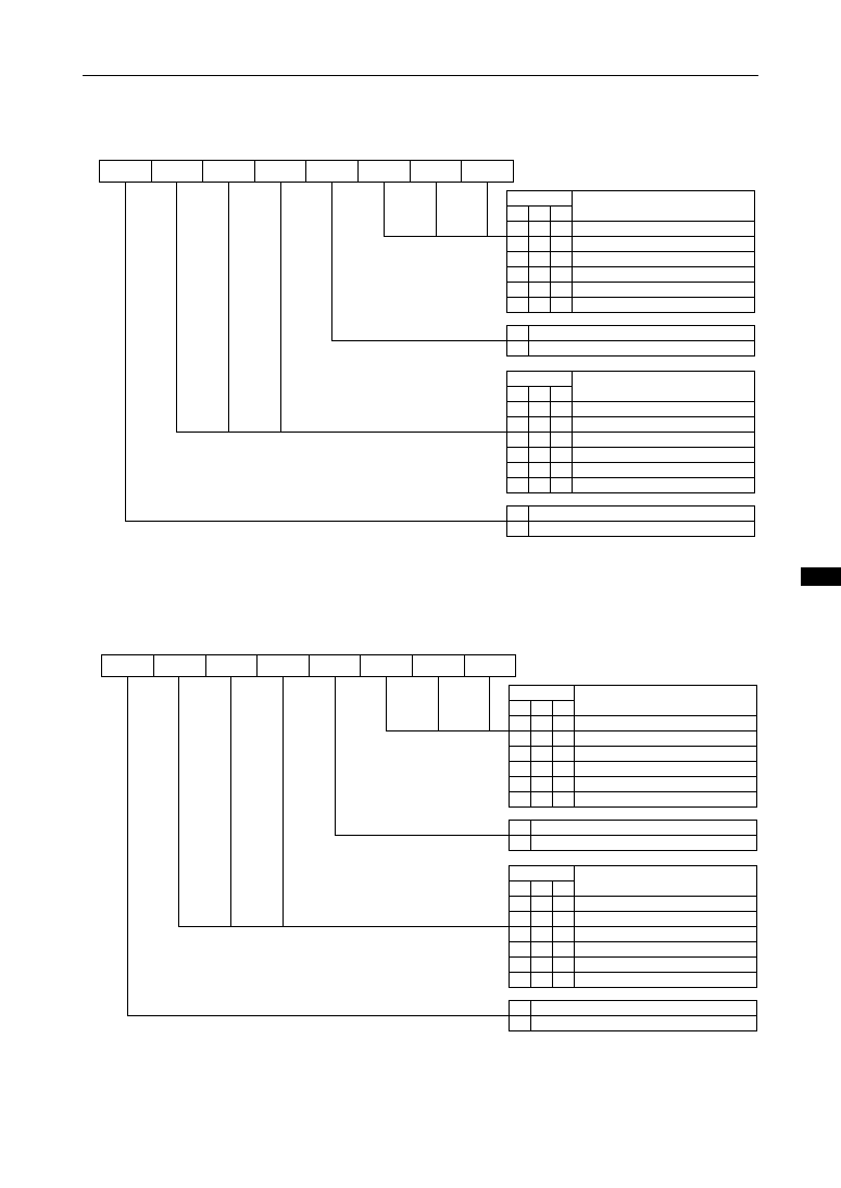
13-7
13
MSM66591/ML66592 User's Manual
Chapter 13 PWM Functions
Figure 13-4 Configuration of PWCON2
Figure 13-5 Configuration of PWCON3
PW5ACT PW5CK2 PW5CK1 PW5CK0 PW4ACT PW4CK2 PW4CK1 PW4CK0
7
6
5
4
3
2
1
0
PW4CK
Count Clock of PWC4
0
0 Master clock
1 TBCCLK
0 1/2 TBCCLK
1 1/4 TBCCLK
0 1/8 TBCCLK
1
0
0
1
1
*
2
0
0
0
0
1
PWM4 high active status
PWM4 low active status
0
1
PW5CK
Count Clock of PWC5
0
0 Master clock
1 TBCCLK
0 1/2 TBCCLK
1 1/4 TBCCLK
0 1/8 TBCCLK
1
0
0
1
1
*
2
0
0
0
0
1
PWM5 high active status
PWM5 low active status
0
1
PWCON2
1 1/16 TBCCLK
*
1
1 1/16 TBCCLK
*
1
"*" indicates either "1" or "0".
PW7ACT PW7CK2 PW7CK1 PW7CK0 PW6ACT PW6CK2 PW6CK1 PW6CK0
7
6
5
4
3
2
1
0
PW6CK
Count Clock of PWC6
0
0 Master clock
1 TBCCLK
0 1/2 TBCCLK
1 1/4 TBCCLK
0 1/8 TBCCLK
1 1/16 TBCCLK
1
0
0
1
1
*
*
2
0
0
0
0
1
1
PWM6 high active status
PWM6 low active status
0
1
PW7CK
Count Clock of PWC7
0
0 Master clock
1 TBCCLK
0 1/2 TBCCLK
1 1/4 TBCCLK
0 1/8 TBCCLK
1 1/16 TBCCLK
1
0
0
1
1
*
*
2
0
0
0
0
1
1
PWM7 high active status
PWM7 low active status
0
1
PWCON3
"*" indicates either "1" or "0".

13-8
MSM66591/ML66592 User's Manual
Chapter 13 PWM Functions
Figure 13-6 Configuration of PWCON4
Figure 13-7 Configuration of PWCON5
PW9ACT PW9CK2 PW9CK1 PW9CK0 PW8ACT PW8CK2 PW8CK1 PW8CK0
7
6
5
4
3
2
1
0
PW8CK
Count Clock of PWC8
0
0 Master clock
1 TBCCLK
0 1/2 TBCCLK
1 1/4 TBCCLK
0 1/8 TBCCLK
1
0
0
1
1
*
2
0
0
0
0
1
PWM8 high active status
PWM8 low active status
0
1
PW9CK
Count Clock of PWC9
0
0 Master clock
1 TBCCLK
0 1/2 TBCCLK
1 1/4 TBCCLK
0 1/8 TBCCLK
1
0
0
1
1
*
2
0
0
0
0
1
PWM9 high active status
PWM9 low active status
0
1
PWCON4
1 1/16 TBCCLK
*
1
1 1/16 TBCCLK
*
1
"*" indicates either "1" or "0".
PW11ACTPW11CK2PW11CK1PW11CK0PW10ACTPW10CK2PW10CK1PW10CK0
7
6
5
4
3
2
1
0
PW10CK
Count Clock of PWC10
0
0 Master clock
1 TBCCLK
0 1/2 TBCCLK
1 1/4 TBCCLK
0 1/8 TBCCLK
1 1/16 TBCCLK
1
0
0
1
1
*
*
2
0
0
0
0
1
1
PWM10 high active status
PWM10 low active status
0
1
PW11CK
Count Clock of PWC11
0
0 Master clock
1 TBCCLK
0 1/2 TBCCLK
1 1/4 TBCCLK
0 1/8 TBCCLK
1 1/16 TBCCLK
1
0
0
1
1
*
*
2
0
0
0
0
1
1
PWM11 high active status
PWM11 low active status
0
1
PWCON5
"*" indicates either "1" or "0".

13-9
13
MSM66591/ML66592 User's Manual
Chapter 13 PWM Functions
[8]
PWMRUN Register (PWRUN)
PWRUN consists of an 8-bit register (PWRUNL) and a 4-bit register (PWRUNH). It
controls the run/stop of PWC0≠PWC11 counter operations.
Figure 13-8 shows the configuration of PWRUNL, and Figure 13-9 the configuration of
PWRUNH.
At reset (when the
RES
signal is input, the BRK instruction is executed, the watchdog
timer is overflown, or an operation code trap is generated), PWRUNL and PWRUNH
become 00H and F0H respectively, and PWC0≠PWC11 stop the count operation.
Figure 13-8 Configuration of PWRUNL
PW7RUN PW6RUN PW5RUN PW4RUN PW3RUN PW2RUN PW1RUN PW0RUN
7
6
5
4
3
2
1
0
0 PWC0 stops
1 PWC0 runs
0 PWC1 stops
1 PWC1 runs
0 PWC2 stops
1 PWC2 runs
0 PWC3 stops
1 PWC3 runs
0 PWC6 stops
1 PWC6 runs
0
1
0 PWC4 stops
1 PWC4 runs
0 PWC5 stops
1 PWC5 runs
PWC7 stops
PWC7 runs
PWRUNL
Figure 13-9 Configuration of PWRUNH
7
6
5
4
3
2
1
0
--
PW11RUN
--
--
--
PW10RUN PW9RUN PW8RUN
1
0
PWC8 runs
PWC8 stops
1
0
PWC9 runs
PWC9 stops
1
0
PWC10 runs
PWC10 stops
1
0
PWC11 runs
"
--
" indicates a bit that is not provided.
"1" is read if a read instruction is executed.
PWC11 stops
PWRUNH

13-10
MSM66591/ML66592 User's Manual
Chapter 13 PWM Functions
[9]
PWM Interrupt Registers (PWINTQ0, PWINTQ1)
Each interrupt request of PWM0≠PWM11 is generated when an underflow of PWC0≠
PWC11 is generated or when the content of PWC0≠PWC11 and that of PWR0≠PWR11
match.
The interrupt vectors corresponding to the interrupt requests generated by PWM0≠
PWM11 are shared by PWM0 and PWM1, by PWM2 and PWM3, by PWM4 and
PWM5, by PWM6 and PWM7, by PWM8 and PWM9, and by PWM10 and PWM11.
PWINTQ0 and PWINTQ1 are 16-bit registers. PWINTQ0 consists of 8-bit registers
PWINTQ0L and PWINTQ0H, and PWINTQ1 consists of 8-bit registers PWINTQ1L and
PWINTQ1H. PWINTQ0 are flags (individual interrupt request flag) that are set to "1" if
an underflow of PWC0≠PWC11 is generated. PWINTQ1 are flags (individual interrupt
request flags) that are set to "1" if the contents of PWC0≠PWC11 and PWR0≠PWR11
match. The bits of PWINTQ0 and PWINTQ1 do not become "0" automatically, even if a
corresponding interrupt occurs. Therefore it is necessary to reset them to "0" by the
program.
If an underflow of PWC0≠PWC11 and a match of the content of PWC0≠PWC11 and
that of PWR0≠PWR11 occur concurrently (when PWR = 0000H is set), the interrupt
request by an underflow of PWC0≠PWC11 is given priority. Therefore, only the corre-
sponding bit of PWINTQ0 is set to "1" and the corresponding bit of PWINTQ1 is not.
Figure 13-10 shows the configuration of PWINTQ0L, Figure 13-11 the configuration of
PWINTQ0H, Figure 13-12 the configuration of PWINTQ1L, and Figure 13-13 the
configuration of PWINTQ1H.
At reset (when the
RES
signal is input, the BRK instruction is executed, the watchdog
timer is overflown, or an operation code trap is generated), PWINTQ0 and PWINTQ1
become F000H.
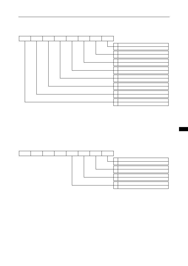
13-11
13
MSM66591/ML66592 User's Manual
Chapter 13 PWM Functions
Figure 13-10 Configuration of PWINTQ0L
Figure 13-11 Configuration of PWINTQ0H
QPW7
QPW6
QPW5
QPW4
QPW3
QPW2
QPW1
QPW0
7
6
5
4
3
2
1
0
0 PWC0 underflow generation: no
1 PWC0 underflow generation: yes
0 PWC1 underflow generation: no
1 PWC1 underflow generation: yes
0 PWC2 underflow generation: no
1 PWC2 underflow generation: yes
0 PWC3 underflow generation: no
1 PWC3 underflow generation: yes
0 PWC6 underflow generation: no
1 PWC6 underflow generation: yes
0
1
0 PWC4 underflow generation: no
1 PWC4 underflow generation: yes
0 PWC5 underflow generation: no
1 PWC5 underflow generation: yes
PWC7 underflow generation: no
PWC7 underflow generation: yes
PWINTQ0L
--
--
--
--
QPW11 QPW10
QPW9
QPW8
7
6
5
4
3
2
1
0
0 PWC8 underflow generation: no
1 PWC8 underflow generation: yes
0 PWC9 underflow generation: no
1 PWC9 underflow generation: yes
0 PWC10 underflow generation: no
1 PWC10 underflow generation: yes
0 PWC11 underflow generation: no
1 PWC11 underflow generation: yes
PWINTQ0H
"
--
" indicates a bit that is not provided.
"1" is read if a read instruction is executed.
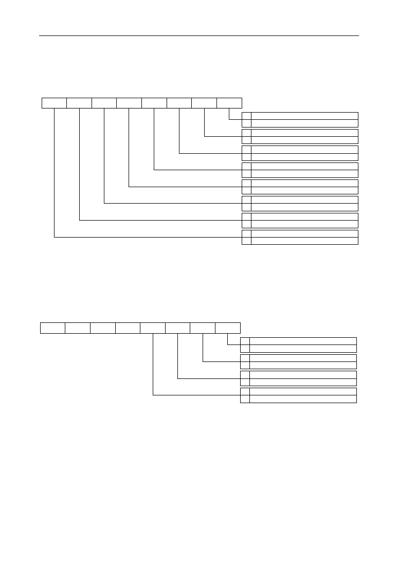
13-12
MSM66591/ML66592 User's Manual
Chapter 13 PWM Functions
Figure 13-12 Configuration of PWINTQ1L
QPWR7 QPWR6 QPWR5 QPWR4 QPWR3 QPWR2 QPWR1 QPWR0
7
6
5
4
3
2
1
0
0 Match of PWC0 and PWR0: no
1 Match of PWC0 and PWR0: yes
0 Match of PWC1 and PWR1: no
1 Match of PWC1 and PWR1: yes
0 Match of PWC2 and PWR2: no
1 Match of PWC2 and PWR2: yes
0 Match of PWC3 and PWR3: no
1 Match of PWC3 and PWR3: yes
0 Match of PWC6 and PWR6: no
1 Match of PWC6 and PWR6: yes
0
1
0 Match of PWC4 and PWR4: no
1 Match of PWC4 and PWR4: yes
0 Match of PWC5 and PWR5: no
1 Match of PWC5 and PWR5: yes
Match of PWC7 and PWR7: no
Match of PWC7 and PWR7: yes
PWINTQ1L
Figure 13-13 Configuration of PWINTQ1H
--
--
--
--
QPWR11 QPWR10 QPWR9 QPWR8
7
6
5
4
3
2
1
0
0 Match of PWC8 and PWR8: no
1 Match of PWC8 and PWR8: yes
0 Match of PWC9 and PWR9: no
1 Match of PWC9 and PWR9: yes
0 Match of PWC10 and PWR10: no
1 Match of PWC10 and PWR10: yes
0 Match of PWC11 and PWR11: no
1 Match of PWC11 and PWR11: yes
PWINTQ1H
"
--
" indicates a bit that is not provided.
"1" is read if a read instruction is executed.

13-13
13
MSM66591/ML66592 User's Manual
Chapter 13 PWM Functions
[10] PWM Interrupt Enable Registers (PWINTE0, PWINTE1)
PWINTE0 and PWINTE1 are 16-bit registers. PWINTE0 consists of 8-bit registers
PWINTE0L and PWINTE0H, and PWINTE1 consists of 8-bit registers PWINTE1L and
PWINTE1H. PWINTE0 is a register that controls enable/disable of the interrupt request
by PWC0≠PWC11 undferflow generation. PWINTE1 is a register that controls enable/
disable of the interrupt request by matching of the contents of PWC0≠PWC11 and
PWR0≠PWR11.
Figure 13-14 shows the configuration of PWINTE0L, Figure 13-15 the configuration of
PWINTE0H, Figure 13-16 the configuration of PWINTE1L, and Figure 13-17 the
configuration of PWINTE1H.
At reset (when the
RES
signal is input, the BRK instruction is executed, the watchdog
timer is overflown, or an operation code trap is generated), PWINTE0 and PWINTE1
become F000H, and the interrupt request of PWM0≠PWM11 is disabled.
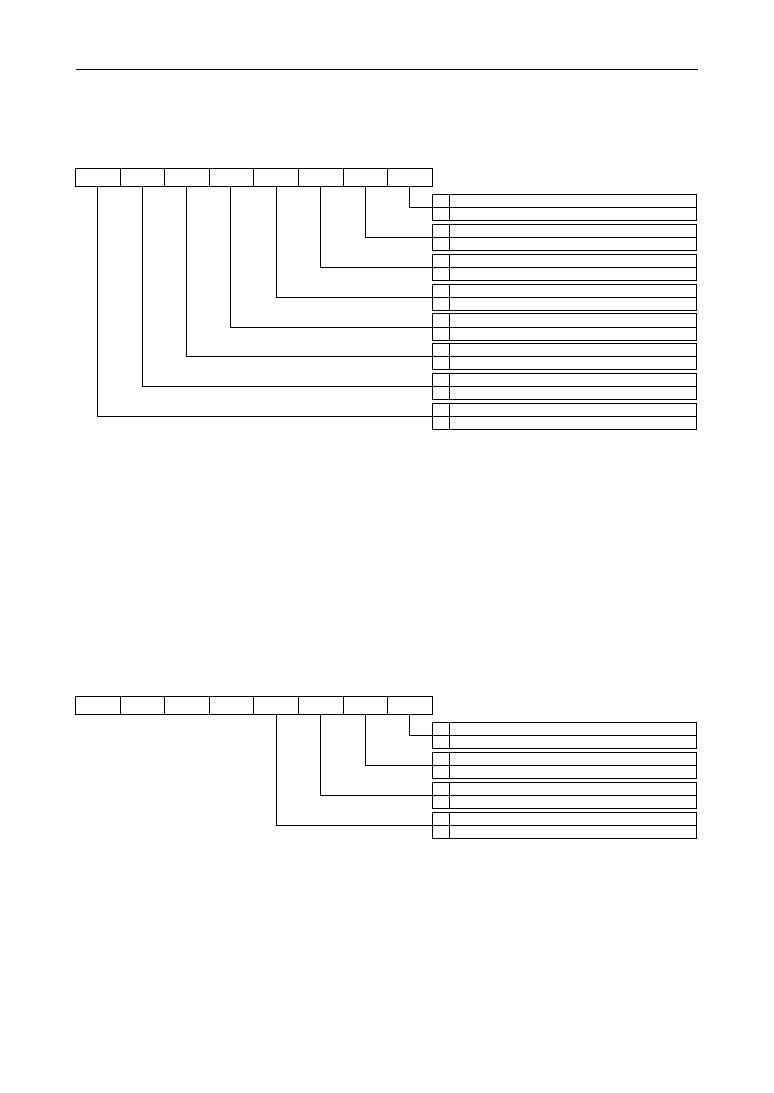
13-14
MSM66591/ML66592 User's Manual
Chapter 13 PWM Functions
Figure 13-14 Configuration of PWINTE0L
Figure 13-15 Configuration of PWINTE0H
EPW7
EPW6
EPW5
EPW4
EPW3
EPW2
EPW1
EPW0
7
6
5
4
3
2
1
0
0
Interrupt request by PWC0 underflow: disabled
1
Interrupt request by PWC0 underflow: enabled
0
Interrupt request by PWC1 underflow: disabled
1
Interrupt request by PWC1 underflow: enabled
0
Interrupt request by PWC2 underflow: disabled
1
Interrupt request by PWC2 underflow: enabled
0
Interrupt request by PWC3 underflow: disabled
1
Interrupt request by PWC3 underflow: enabled
0
Interrupt request by PWC6 underflow: disabled
1
Interrupt request by PWC6 underflow: enabled
0
1
0
Interrupt request by PWC4 underflow: disabled
1
Interrupt request by PWC4 underflow: enabled
0
Interrupt request by PWC5 underflow: disabled
1
Interrupt request by PWC5 underflow: enabled
Interrupt request by PWC7 underflow: disabled
Interrupt request by PWC7 underflow: enabled
PWINTE0L
--
--
--
--
EPW11
EPW10
EPW9
EPW8
7
6
5
4
3
2
1
0
0
Interrupt request by PWC8 underflow: disabled
1
Interrupt request by PWC8 underflow: enabled
0
Interrupt request by PWC9 underflow: disabled
1
Interrupt request by PWC9 underflow: enabled
0
Interrupt request by PWC10 underflow: disabled
1
Interrupt request by PWC10 underflow: enabled
0
Interrupt request by PWC11 underflow: disabled
1
Interrupt request by PWC11 underflow: enabled
PWINTE0H
"--" indicates a bit that is not provided.
"1" is read if a read instruction is executed.
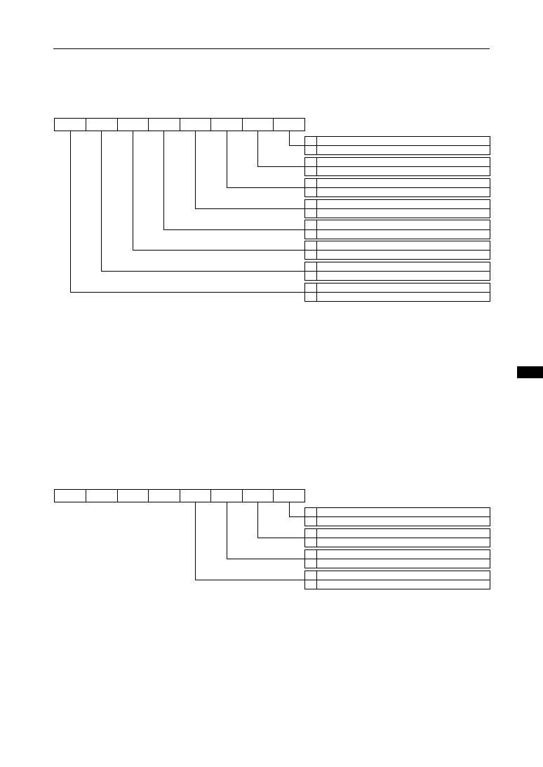
13-15
13
MSM66591/ML66592 User's Manual
Chapter 13 PWM Functions
Figure 13-16 Configuration of PWINTE1L
EPWR7 EPWR6 EPWR5 EPWR4 EPWR3 EPWR2 EPWR1 EPWR0
7
6
5
4
3
2
1
0
0
Interrupt request by match of PWC0 and PWR0 : disabled
1
Interrupt request by match of PWC0 and PWR0 : enabled
0
Interrupt request by match of PWC1 and PWR1 : disabled
1
Interrupt request by match of PWC1 and PWR1 : enabled
0
Interrupt request by match of PWC2 and PWR2 : disabled
1
Interrupt request by match of PWC2 and PWR2 : enabled
0
Interrupt request by match of PWC3 and PWR3 : disabled
1
Interrupt request by match of PWC3 and PWR3 : enabled
0
Interrupt request by match of PWC6 and PWR6 : disabled
1
Interrupt request by match of PWC6 and PWR6 : enabled
0
1
0
Interrupt request by match of PWC4 and PWR4 : disabled
1
Interrupt request by match of PWC4 and PWR4 : enabled
0
Interrupt request by match of PWC5 and PWR5 : disabled
1
Interrupt request by match of PWC5 and PWR5 : enabled
Interrupt request by match of PWC7 and PWR7 : disabled
Interrupt request by match of PWC7 and PWR7 : enabled
PWINTE1L
Figure 13-17 Configuration of PWINTE1H
--
--
--
--
EPWR11 EPWR10 EPWR9 EPWR8
7
6
5
4
3
2
1
0
0
Interrupt request by match of PWC8 and PWR8 : disabled
1
Interrupt request by match of PWC8 and PWR8 : enabled
0
Interrupt request by match of PWC9 and PWR9 : disabled
1
Interrupt request by match of PWC9 and PWR9 : enabled
0
Interrupt request by match of PWC10 and PWR10 : disabled
1
Interrupt request by match of PWC10 and PWR10 : enabled
0
Interrupt request by match of PWC11 and PWR11 : disabled
1
Interrupt request by match of PWC11 and PWR11 : enabled
PWINTE1H
"--" indicates a bit that is not provided.
"1" is read if a read instruction is executed.

13-16
MSM66591/ML66592 User's Manual
Chapter 13 PWM Functions
13.2 Operation of PWM
PWM0≠PWM11 control duty within a specific cycle (determined by the count clock of
PWC0≠PWC11 or by the contents of PWC0≠PWC11 and PWC0BF≠PWC11BF).
PWM is started by setting the corresponding RUN bit to "1". If the RUN bit becomes "1",
the output F/F is set to "1" at the same time, and "H" level is output to the PWM output
pin (in the case of high active status.) If the contents of the corresponding PWC0≠
PWC11 and PWR0≠PWR11 match, the output F/F is set to "0", "L" level is output to the
PWM output pin and an individual interrupt request flag is set to "1". If PWC0≠PWC11
generate an underflow, the output F/F is set to "1", "H" level is output to the PWM
output pin, an individual interrupt request flag is set to "1", and, at the same time, the
contents of PWC0BF≠PWC11BF and PW0BF≠PW11BF are loaded to PWC0≠PWC11
and PWR0≠PWR11, respectively. This operation is repeated, and the duty-controlled
waveform is output from the PWM output pin until the RUN bit is set to "0".
If an underflow of PWC0≠PWC11 and a match of the contents of PWC0≠PWC11 and
PWR0≠PWR11 occur concurrently (when PWR = 0000H is set), the interrupt request by
an underflow of PWC0≠PWC11 is given priority. Therefore, only the individual interrupt
request flag by the underflow of PWC0≠PWC11 is set to "1"; the individual interrupt
request flag by the match of the contents of PWC0≠PWC11 and PWR0≠PWR11 is not
set to "1".
The duty immediately after PWM start may become shorter (only 1 cycle), depending
on the selected count clock of PWC0≠PWC11. Refer to the following example.
Maximum Errors
TBCCLK
≠(TBCCLK ≠ 1 CLK)
1/2 TBCCLK
≠(1/2 TBCCLK ≠ 1 CLK)
1/4 TBCCLK
1/8 TBCCLK
0
≠(1/4 TBCCLK ≠ 1 CLK)
≠(1/8 TBCCLK ≠ 1 CLK)
Master Clock (CLK)
Count Clock
1/16 TBCCLK
≠(1/16 TBCCLK ≠ 1 CLK)
1/32 TBCCLK
≠(1/32 TBCCLK ≠ 1 CLK)
If a different clock is used for the PWC clock with the equal value set for PWCn and
PWCnBF (n = 0≠11) and PWnRUN bit is set to "1" at the same time, the cycle will be
equal, however a synchronization shift may occur.
If the PWCn and PWCnBF (n = 0≠11) values are both FFFFH, and in high active status,
PWM becomes 1/65536 duty output when PWR is FFFFH. If the PWR value is de-
creased, the output duty ("H" level period) increases. If the PWR value is 0000H, output
becomes 65536/65536 at 100% duty. 0/65536, which is 0% duty, cannot be imple-
mented in a PWM block.
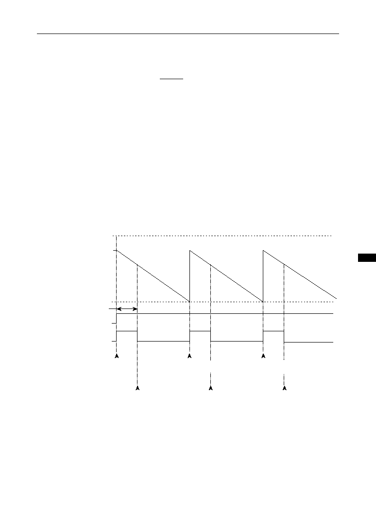
13-17
13
MSM66591/ML66592 User's Manual
Chapter 13 PWM Functions
Figure 13-18 PWM Output Operation Example (in high active status)
The calculation of a PWM cycle is shown below.
f
(PWM)
= f
(OSC)
•
PWCLK
•
f
(PWM)
: cycle of PWM (Hz)
f
(OSC)
: master clock frequency (Hz)
PWCLK: input clock of PWM
N: PWCn and PWCnBF value (n = 0≠11)
[Example]
Master clock frequency: 24 MHz; input clock of PWM: TBCCLK (dividing ratio of the 1/n
counter: 1/4); PWCnBF value: 00FFH
f
(PWM)
= 24,000,000
•
1/4
•
1/(255 + 1) = 93,750 Hz
(10.67
µ
sec)
Figure 13-18 shows an example of PWM output operation. Figure 13-19 shows an
example of a PWM output timing change.
Content of PWC
PWR value
PWnRUN bit
PWM output waveform
FFFFH
0H (UDF)
PWnRUN bit
is set
(n = 0≠11)
PWC = PWR
(interrupt req. is generated)
PWC underflow is generated
(interrupt req. is generated)
PWC = PWR
(interrupt req. is generated)
PWC underflow is generated
(interrupt req. is generated)
PWC = PWR
(interrupt req. is generated)
1
N + 1
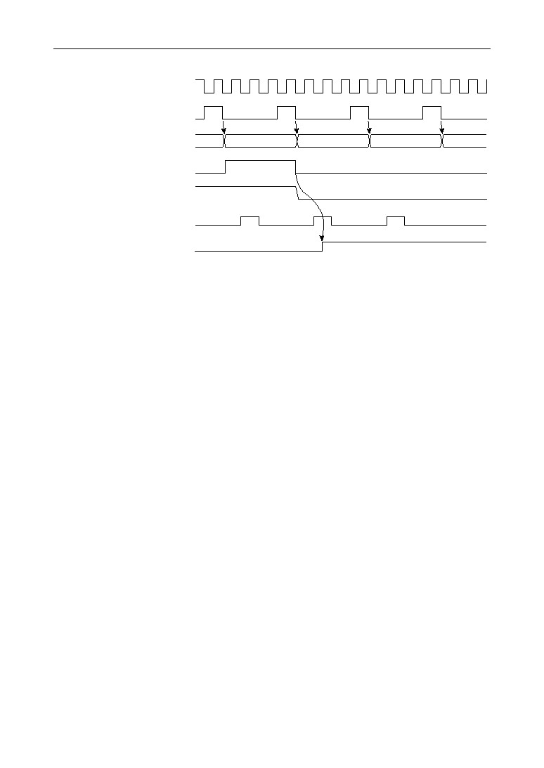
13-18
MSM66591/ML66592 User's Manual
Chapter 13 PWM Functions
Figure 13-19 PWM Output Timing Change Example
100H
0FFH
0FEH
PWC clock: TBCCLK
(dividing ratio of the 1/n counter: 1/4)
Master clock (CLK)
Content of PWC
Match signal of PWC and PWR
Change of PWM output pin
MIS1
IRQ

Baud Rate Generator
Functions
Chapter 14
14


14-1
14
MSM66591/ML66592 User's Manual
Chapter 14 Baud Rate Generator Functions
Figure 14-1 Configuration of S0TM, S1TM, S2TM, S3TM, S4TM
14. Baud Rate Generator Functions
The MSM66591/ML66592 have five serial communication functions: the UART serial
ports 0, 2, 3, 4 and the synchronous/UART serial port 1. Each serial port has 8-bit
timers (S0TM, S1TM, S2TM, S3TM, S4TM) that can be used as baud rate generators.
When not used as baud rate generators, these timers can be used as 8-bit auto reload
timers.
The basic configuration of S0TM, S1TM, S2TM, S3TM and S4TM is the same, except
for the address of registers located in the SFR area.
Interrupts for S0TM, S1TM, S2TM, S3TM and S4TM are assigned to the same interrupt
vector. The generation of individual interrupt requests are enabled or disabled by bit 3
(ESTMn) of each timer control register (SnCON). Verification of whether an interrupt
request has been generated is performed based on bit 2 (QSTMn) of each timer control
register. (n = 0≠4)
Figure 14-1 shows the configuration of S0TM, S1TM, S2TM, S3TM and S4TM. Table
14-1 lists the S0TM, S1TM, S2TM, S3TM and S4TM control SFRs.
Master clock (CLK)
1/2 CLK
1/2 TBCCLK
1/4 TBCCLK
1/8 TBCCLK
1/16 TBCCLK
1/64 TBCCLK
1/256 TBCCLK
Selector
SCIn Timer Counter
SCIn Timer Register
Interrupt
request
SnCON
OVF
Baud rate clock for
SCIn
(n = 0≠4)
QSTMn
ESTMn
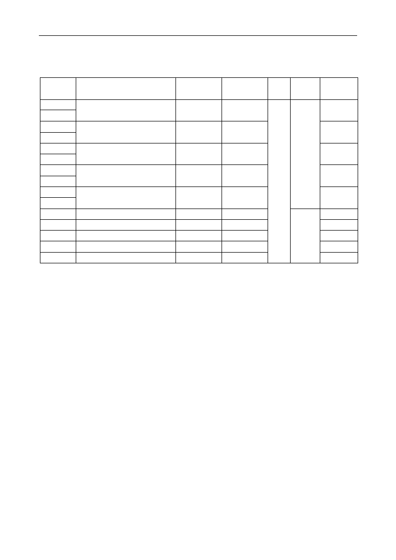
14-2
MSM66591/ML66592 User's Manual
Chapter 14 Baud Rate Generator Functions
Table 14-1 S0TM, S1TM, S2TM, S3TM, S4TM Control SFRs
0120
SCI0 Timer
--
0121
0122
0123
0124
0125
R/W
0000
16
S0TM
0126
0127
0128
0129
012A
012B
012C
012D
012E
SCI1 Timer
SCI2 Timer
SCI3 Timer
SCI4 Timer
SCI0 Timer Control Register
SCI1 Timer Control Register
SCI2 Timer Control Register
SCI3 Timer Control Register
SCI4 Timer Control Register
S0CON
--
S1CON
--
S2CON
--
S3CON
--
S4CON
--
--
S1TM
--
S2TM
--
S3TM
--
S4TM
0000
0000
0000
0000
02
02
02
02
02
8
Some addresses are not consecutive.
Addresses in the address column marked by "" indicate that the register has bits missing.
Address [H]
Name
Abbreviated
Name (BYTE)
R/W
8/16-Bit
Operation
Reset
State [H]
Abbreviated
Name (WORD)

14-3
14
MSM66591/ML66592 User's Manual
Chapter 14 Baud Rate Generator Functions
14.1 Configuration of SCI0 Timer (S0TM)
The SCI0 timer (S0TM) consists of an 8-bit SCI0 timer counter, an 8-bit SCI0 timer
register that stores the reload values of the SCI0 timer counter, and a control register
(S0CON) that specifies the timer counter operations.
[1]
SCI0 Timer Counter (low-order 8 bits of 16-bit register S0TM)
The SCI0 timer counter is an 8-bit counter. When S0TM overflows, an interrupt request
is generated, and the content of the 8-bit SCI0 timer register is loaded to SCI0 timer
counter. The count clock of S0TM is selected by the high-order 3 bits (bits 5≠7) of the
8-bit SCI0 timer control register (S0CON).
[2]
SCI0 Timer Register (high-order 8 bits of 16-bit register S0TM)
The SCI0 timer register is an 8-bit register. The content of the register is loaded to the
SCI0 timer counter when the counter overflows.
The SCI0 timer counter and SCI0 timer register are accessible only as a 16-bit S0TM
which uses the SCI0 timer counter as its low-order 8 bits and the SCI0 timer register as
its high-order 8 bits.
At reset (when the
RES
signal is input, the BRK instruction is executed, the watchdog
timer is overflown, or an operation code trap is generated), S0TM becomes 0000H, and
the count operation stops.
[3]
SCI0 Timer Control Register (S0CON)
S0CON is an 8-bit register. The high-order 4 bits (bits 4≠7) select the count clock of
S0TM, and controls the start/stop of the count operation. The low-order 2 bits (bits 2
and 3) perform interrupt related controls. The least significant bit (bit 0) specifies the
mode of S0TM.
At reset (when the
RES
signal is input, the BRK instruction is executed, the watchdog
timer is overflown, or an operation code trap is generated), S0CON becomes 02H, a
CLK is selected as the count clock of S0TM, the auto reload timer mode is selected,
and operation stops.
Figure 14-2 shows the configuration of S0CON.
<Description of Each Bit>
∑ S0MOD (bit 0)
This bit specifies the operation mode of S0TM. If this bit is "0", S0TM operates in
auto reload timer mode. If "1", S0TM operates in SCI0 baud rate generator mode.
∑ QSTM0 (bit 2)
This bit becomes "1" if an SCI0 timer counter overflow is generated. Since this bit
does not become "0" automatically after an interrupt process is executed, it is
necessary to set to "0" by the program.
∑ ESTM0 (bit 3)
This bit enables/disables an interrupt request generation by an SCI0 timer counter
overflow. If this bit is "1", generation is enabled, and if "0", generation is disabled.
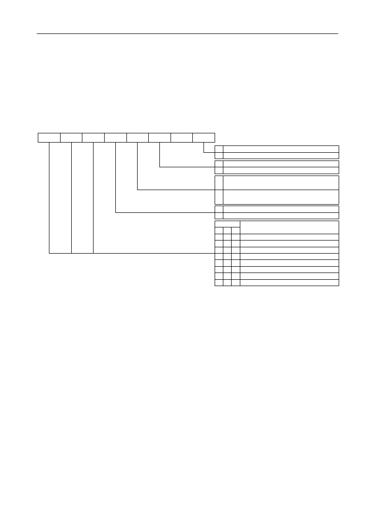
14-4
MSM66591/ML66592 User's Manual
Chapter 14 Baud Rate Generator Functions
∑ S0RUN (bit 4)
This bit specifies the RUN/STOP of the SCI0 timer counter. If this bit is "0", the SCI0
timer counter stops, and if "1", it runs.
∑ S0CK0≠S0CK2 (bits 5≠7)
These three bits specify the count clock of the SCI0 timer counter.
Figure 14-2 Configuration of S0CON
S0CK2 S0CK1 S0CK0 S0RUN ESTM0 QSTM0
--
S0MOD
7
6
5
4
3
2
1
0
0 S0TM auto-reload timer mode
1 S0TM baud rate generator mode for SCI0
0 SCI0 timer counter overflow generation:no
1 SCI0 timer counter overflow generation:yes
0 SCI0 timer counter count operation STOP
1 SCI0 timer counter count operation RUN
S0CK
Count Clock of S0TM
2 1 0
0 0 0 Master clock (CLK)
0 0 1 1/2 CLK
0 1 0 1/2 TBCCLK
0 1 1 1/4 TBCCLK
1 0 0 1/8 TBCCLK
1 0 1 1/16 TBCCLK
1 1 0 1/64 TBCCLK
1 1 1 1/256 TBCCLK
"--" indicates a bit that is not provided.
"1" is read if a read instruction is executed.
S0CON
0
SCI0 timer counter overflow interrupt
request generation disabled
1
SCI0 timer counter overflow interrupt
request generation enabled

14-5
14
MSM66591/ML66592 User's Manual
Chapter 14 Baud Rate Generator Functions
1
256 ≠ D
14.2 Operation of SCI0 Timer
Basically the SCI0 timer operates as an auto reload timer. If the 8-bit SCI0 timer
counter overflows, the value of the 8-bit SCI0 timer register is loaded to the counter. At
the same time, an interrupt request by overflow is generated. The calculation of the
baud rate when SCI0 is used as the baud rate generator is shown below.
B: baud rate
f
(BRG)
: S0TM count clock frequency (Hz)
D: reload value (0 to 255)
Even if the reload value is written to the SCI0 timer register, the content of the SCI0
timer counter does not change. If the SCI0 timer is used as the auto reload timer (baud
rate generator) from the beginning of an operation, it is necessary to write the same
value to both the SCI0 timer counter and SCI0 timer register by the program.
B = f
(BRG)
•
•
1
16

14-6
MSM66591/ML66592 User's Manual
Chapter 14 Baud Rate Generator Functions
14.3 Configuration of SCI1 Timer (S1TM)
The SCI1 timer (S1TM) consists of an 8-bit SCI1 timer counter, an 8-bit SCI1 timer
register that stores the reload values of the SCI1 timer counter, and a control register
(S1CON) that specifies S1TM operations.
[1]
SCI1 Timer Counter (low-order 8 bits of 16-bit register S1TM)
The SCI1 timer counter is an 8-bit counter. When S1TM overflows, an interrupt request
is generated, and the content of the 8-bit SCI1 timer register is loaded to SCI1 timer
counter. The count clock of S1TM is selected by the high-order 3 bits (bits 5≠7) of the
8-bit SCI1 timer control register (S1CON).
[2]
SCI1 Timer Register (high-order 8 bits of 16-bit register S1TM)
The SCI1 timer register is an 8-bit register. The content of the register is loaded to the
SCI1 timer counter when the counter overflows.
The SCI1 timer counter and SCI1 timer register are accessible only as a16-bit S1TM
which uses the SCI1 timer counter as its low-order 8 bits and the SCI1 timer register as
its high-order 8 bits.
At reset (when the
RES
signal is input, the BRK instruction is executed, the watchdog
timer is overflown, or an operation code trap is generated), S1TM becomes 0000H, and
the count operation stops.
[3]
SCI1 Timer Control Register (S1CON)
S1CON is an 8-bit register. The high-order 4 bits (bits 4≠7) select the count clock of
S1TM, and control the start/stop of the count operation. The low-order 2 bits (bits 2, 3)
perform interrupt related controls. The least significant bit (bit 0) specifies the mode of
S1TM.
At reset (when the
RES
signal is input, the BRK instruction is executed, the watchdog
timer is overflown, or an operation code trap is generated), S1CON becomes 02H, a
CLK is selected as the count clock of S1TM, the auto-reload timer mode is selected,
and operation stops.
Figure 14-3 shows the configuration of S1CON.
<Description of Each Bit>
∑ S1MOD (bit 0)
This bit specifies the operation mode of S1TM. If this bit is "0", S1TM operates in
auto reload mode. If "1", S1TM operates in SCI1 baud rate generator mode.
∑ QSTM1 (bit 2)
This bit becomes "1" if an SCI1 timer counter overflow is generated. Since this bit
does not become "0" automatically after an interrupt process is executed, it is
necessary to set to "0" by the program.
∑ ESTM1 (bit 3)
This bit enables/disables an interrupt request generation by an SCI1 timer counter
overflow. If this bit is "1", generation is enabled, and if "0", generation is disabled.
14-7
14
MSM66591/ML66592 User's Manual
Chapter 14 Baud Rate Generator Functions
Figure 14-3 Configuration of S1CON
∑ S1RUN (bit 4)
This bit specifies the RUN/STOP of the SCI1 timer counter. If this bit is "0", the SCI1
timer counter stops, and if "1", it runs.
∑ S1CK0≠S1CK2 (bits 5≠7)
These three bits specify the count clock of the SCI1 timer counter.
S1CK2 S1CK1 S1CK0 S1RUN ESTM1 QSTM1
--
S1MOD
7
6
5
4
3
2
1
0
0 S1TM auto-reload timer mode
1 S1TM baud rate generator mode for SCI1
0 SCI1 timer counter overflow generation:no
1 SCI1 timer counter overflow generation:yes
0 SCI1 timer counter count operation STOP
1 SCI1 timer counter count operation RUN
S1CK
Count Clock of S1TM
2 1 0
0 0 0 Master clock (CLK)
0 0 1 1/2 CLK
0 1 0 1/2 TBCCLK
0 1 1 1/4 TBCCLK
1 0 0 1/8 TBCCLK
1 0 1 1/16 TBCCLK
1 1 0 1/64 TBCCLK
1 1 1 1/256 TBCCLK
"--" indicates a bit that is not provided.
"1" is read if a read instruction is executed.
S1CON
0
SCI1 timer counter overflow interrupt
request generation disabled
1
SCI1 timer counter overflow interrupt
request generation enabled

14-8
MSM66591/ML66592 User's Manual
Chapter 14 Baud Rate Generator Functions
14.4 Operation of SCI1 Timer
Basically the SCI1 timer operates as the auto-reload timer. If the 8-bit timer counter
(S1TM) overflows, the value of the 8-bit register (S1TMR) is loaded. At the same time,
an interrupt request by an overflow is generated. The calculation of the baud rate when
SCI1 is used as the baud rate generator is shown below.
UART mode:
B: baud rate
f
(BRG)
: S1TM count clock frequency (Hz)
D: reload value (0 to 255)
Synchronous mode:
B: baud rate
f
(BRG)
: S1TM count clock frequency (Hz)
D: reload value (0 to 255)
Even if the reload value is written to the SCI1 timer register, the content of the SCI1
timer counter does not change. If the SCI1 timer is used as the auto reload timer (baud
rate generator) from the beginning of operation, it is necessary to write the same value
to both the SCI1 timer counter and SCI1 timer register through programming.
B = f
(BRG)
•
•
B = f
(BRG)
•
•
16
1
1
4
256 ≠ D
1
256 ≠ D
1

14-9
14
MSM66591/ML66592 User's Manual
Chapter 14 Baud Rate Generator Functions
14.5 Configuration of SCI2 Timer (S2TM)
The SCI2 timer (S2TM) consists of an 8-bit SCI2 timer counter, an 8-bit SCI2 timer
register that stores the reload values of the SCI2 timer counter, and a control register
(S2CON) that specifies S2TM operations.
[1]
SCI2 Timer Counter (low-order 8 bits of 16-bit register S2TM)
The SCI2 timer counter is an 8-bit counter. When S2TM overflows, an interrupt request
is generated, and the content of the 8-bit SCI2 timer register is loaded to SCI2 timer
counter. The count clock of S2TM is selected by the high-order 3 bits (bits 5≠7) of the
8-bit SCI2 timer control register (S2CON).
[2]
SCI2 Timer Register (high-order 8 bits of 16-bit register S2TM)
The SCI2 timer register is an 8-bit register. The content of the register is loaded to the
SCI2 timer counter when the counter overflows.
The SCI2 timer counter and SCI2 timer register are accessible only as a 16-bit S2TM
which uses the SCI2 timer counter as its low-order 8 bits and the SCI2 timer register as
its high-order 8 bits.
At reset (when the
RES
signal is input, the BRK instruction is executed, the watchdog
timer is overflown, or an operation code trap is generated), S2TM becomes 0000H, and
the count operation stops.
[3]
SCI2 Timer Control Register (S2CON)
S2CON is an 8-bit register. The high-order 4 bits (bits 4≠7) select the count clock of
S2TM, and controls the start/stop of the count operation. The low-order 2 bits (bits 2
and 3) perform interrupt related controls. The least significant bit (bit 0) specifies the
mode of S2TM.
At reset (when the
RES
signal is input, the BRK instruction is executed, the watchdog
timer is overflown, or an operation code trap is generated), S2CON becomes 02H, a
CLK is selected as the count clock of S2TM, the auto reload timer mode is selected,
and operation stops.
Figure 14-4 shows the configuration of S2CON.
<Description of Each Bit>
∑ S2MOD (bit 0)
This bit specifies the operation mode of S2TM. If this bit is "0", S2TM operates in
auto reload timer mode. If "1", S2TM operates in SCI2 baud rate generator mode.
∑ QSTM2 (bit 2)
This bit becomes "1" if an SCI2 timer counter overflow is generated. Since this bit
does not become "0" automatically after an interrupt process is executed, it is
necessary to set to "0" by the program.
∑ ESTM2 (bit 3)
This bit enables/disables an interrupt request generation by an SCI2 timer counter
overflow. If this bit is "1", generation is enabled, and if "0", generation is disabled.

14-10
MSM66591/ML66592 User's Manual
Chapter 14 Baud Rate Generator Functions
∑ S2RUN (bit 4)
This bit specifies the RUN/STOP of the SCI2 timer counter. If this bit is "0", the SCI2
timer counter stops, and if "1", it runs.
∑ S2CK0≠S2CK2 (bits 5≠7)
These three bits specify the count clock of the SCI2 timer counter.
Figure 14-4 Configuration of S2CON
S2CK2 S2CK1 S2CK0 S2RUN ESTM2 QSTM2
--
S2MOD
7
6
5
4
3
2
1
0
0 S2TM auto-reload timer mode
1 S2TM baud rate generator mode for SCI2
0 SCI2 timer counter overflow generation:no
1 SCI2 timer counter overflow generation:yes
0 SCI2 timer counter count operation STOP
1 SCI2 timer counter count operation RUN
S2CK
Count Clock of S2TM
2 1 0
0 0 0 Master clock (CLK)
0 0 1 1/2 CLK
0 1 0 1/2 TBCCLK
0 1 1 1/4 TBCCLK
1 0 0 1/8 TBCCLK
1 0 1 1/16 TBCCLK
1 1 0 1/64 TBCCLK
1 1 1 1/256 TBCCLK
"--" indicates a bit that is not provided.
"1" is read if a read instruction is executed.
S2CON
0
SCI2 timer counter overflow interrupt
request generation disabled
1
SCI2 timer counter overflow interrupt
request generation enabled

14-11
14
MSM66591/ML66592 User's Manual
Chapter 14 Baud Rate Generator Functions
1
256 ≠ D
14.6 Operation of SCI2 Timer
Basically the SCI2 timer operates as an auto reload timer. If the 8-bit SCI2 timer
counter overflows, the value of the 8-bit SCI2 timer register is loaded to the counter. At
the same time, an interrupt request by overflow is generated. The calculation of the
baud rate when SCI2 is used as the baud rate generator is shown below.
B: baud rate
f
(BRG)
: S2TM count clock frequency (Hz)
D: reload value (0 to 255)
Even if the reload value is written to the SCI2 timer register, the content of the SCI2
timer counter does not change. If the SCI2 timer is used as the auto reload timer (baud
rate generator) from the beginning of an operation, it is necessary to write the same
value to both the SCI2 timer counter and SCI2 timer register through programming.
B = f
(BRG)
•
•
1
16

14-12
MSM66591/ML66592 User's Manual
Chapter 14 Baud Rate Generator Functions
14.7 Configuration of SCI3 Timer (S3TM)
The SCI3 timer (S3TM) consists of an 8-bit SCI3 timer counter, an 8-bit SCI3 timer
register that stores the reload values of the SCI3 timer counter, and a control register
(S3CON) that specifies S3TM operations.
[1]
SCI3 Timer Counter (low-order 8 bits of 16-bit register S3TM)
The SCI3 timer counter is an 8-bit counter. When S3TM overflows, an interrupt request
is generated, and the content of the 8-bit SCI3 timer register is loaded to SCI3 timer
counter. The count clock of S3TM is selected by the high-order 3 bits (bits 5≠7) of the
8-bit SCI3 timer control register (S3CON).
[2]
SCI3 Timer Register (high-order 8 bits of 16-bit register S3TM)
The SCI3 timer register is an 8-bit register. The content of the register is loaded to the
SCI3 timer counter when the counter overflows.
The SCI3 timer counter and SCI3 timer register are accessible only as a 16-bit S3TM
which uses the SCI3 timer counter as its low-order 8 bits and the SCI3 timer register as
its high-order 8 bits.
At reset (when the
RES
signal is input, the BRK instruction is executed, the watchdog
timer is overflown, or an operation code trap is generated), S3TM becomes 0000H, and
the count operation stops.
[3]
SCI3 Timer Control Register (S3CON)
S3CON is an 8-bit register. The high-order 4 bits (bits 4≠7) select the count clock of
S3TM, and controls the start/stop of the count operation. The low-order 2 bits (bits 2
and 3) perform interrupt related controls. The least significant bit (bit 0) specifies the
mode of S3TM.
At reset (when the
RES
signal is input, the BRK instruction is executed, the watchdog
timer is overflown, or an operation code trap is generated), S3CON becomes 02H, a
CLK is selected as the count clock of S3TM, the auto reload timer mode is selected,
and operation stops.
Figure 14-5 shows the configuration of S3CON.
<Description of Each Bit>
∑ S3MOD (bit 0)
This bit specifies the operation mode of S3TM. If this bit is "0", S3TM operates in
auto reload timer mode. If "1", S3TM operates in SCI3 baud rate generator mode.
∑ QSTM3 (bit 2)
This bit becomes "1" if an SCI3 timer counter overflow is generated. Since this bit
does not become "0" automatically after an interrupt process is executed, it is
necessary to set to "0" by the program.
∑ ESTM3 (bit 3)
This bit enables/disables an interrupt request generation by an SCI3 timer counter
overflow. If this bit is "1", generation is enabled, and if "0", generation is disabled.
14-13
14
MSM66591/ML66592 User's Manual
Chapter 14 Baud Rate Generator Functions
∑ S3RUN (bit 4)
This bit specifies the RUN/STOP of the SCI3 timer counter. If this bit is "0", the SCI3
timer counter stops, and if "1", it runs.
∑ S3CK0≠S3CK2 (bits 5≠7)
These three bits specify the count clock of the SCI3 timer counter.
Figure 14-5 Configuration of S3CON
S3CK2 S3CK1 S3CK0 S3RUN ESTM3 QSTM3
--
S3MOD
7
6
5
4
3
2
1
0
0 S3TM auto-reload timer mode
1 S3TM baud rate generator mode for SCI3
0 SCI3 timer counter overflow generation:no
1 SCI3 timer counter overflow generation:yes
0 SCI3 timer counter count operation STOP
1 SCI3 timer counter count operation RUN
S3CK
Count Clock of S3TM
2 1 0
0 0 0 Master clock (CLK)
0 0 1 1/2 CLK
0 1 0 1/2 TBCCLK
0 1 1 1/4 TBCCLK
1 0 0 1/8 TBCCLK
1 0 1 1/16 TBCCLK
1 1 0 1/64 TBCCLK
1 1 1 1/256 TBCCLK
"--" indicates a bit that is not provided.
"1" is read if a read instruction is executed.
S3CON
0
SCI3 timer counter overflow interrupt
request generation disabled
1
SCI3 timer counter overflow interrupt
request generation enabled

14-14
MSM66591/ML66592 User's Manual
Chapter 14 Baud Rate Generator Functions
1
256 ≠ D
14.8 Operation of SCI3 Timer
Basically the SCI3 timer operates as an auto reload timer. If the 8-bit SCI3 timer
counter overflows, the value of the 8-bit SCI3 timer register is loaded to the counter. At
the same time, an interrupt request by overflow is generated. The calculation of the
baud rate when SCI3 is used as the baud rate generator is shown below.
B: baud rate
f
(BRG)
: S3TM count clock frequency (Hz)
D: reload value (0 to 255)
Even if the reload value is written to the SCI3 timer register, the content of the SCI3
timer counter does not change. If the SCI3 timer is used as the auto reload timer (baud
rate generator) from the beginning of an operation, it is necessary to write the same
value to both the SCI3 timer counter and SCI3 timer register through programming.
B = f
(BRG)
•
•
1
16

14-15
14
MSM66591/ML66592 User's Manual
Chapter 14 Baud Rate Generator Functions
14.9 Configuration of SCI4 Timer (S4TM)
The SCI4 timer (S4TM) consists of an 8-bit SCI4 timer counter, an 8-bit SCI4 timer
register that stores the reload values of the SCI4 timer counter, and a control register
(S4CON) that specifies S4TM operations.
[1]
SCI4 Timer Counter (low-order 8 bits of 16-bit register S4TM)
The SCI4 timer counter is an 8-bit counter. When S4TM overflows, an interrupt request
is generated, and the content of the 8-bit SCI4 timer register is loaded to SCI4 timer
counter. The count clock of S4TM is selected by the high-order 3 bits (bits 5≠7) of the
8-bit SCI4 timer control register (S4CON).
[2]
SCI4 Timer Register (high-order 8 bits of 16-bit register S4TM)
The SCI4 timer register is an 8-bit register. The content of the register is loaded to the
SCI4 timer counter when the counter overflows.
The SCI4 timer counter and SCI4 timer register are accessible only as a 16-bit S4TM
which uses the SCI4 timer counter as its low-order 8 bits and the SCI4 timer register as
its high-order 8 bits.
At reset (when the
RES
signal is input, the BRK instruction is executed, the watchdog
timer is overflown, or an operation code trap is generated), S4TM becomes 0000H, and
the count operation stops.
[3]
SCI4 Timer Control Register (S4CON)
S4CON is an 8-bit register. The high-order 4 bits (bits 4≠7) select the count clock of
S4TM, and controls the start/stop of the count operation. The low-order 2 bits (bits 2
and 3) perform interrupt related controls. The least significant bit (bit 0) specifies the
mode of S4TM.
At reset (when the
RES
signal is input, the BRK instruction is executed, the watchdog
timer is overflown, or an operation code trap is generated), S4CON becomes 02H, a
CLK is selected as the count clock of S4TM, the auto reload timer mode is selected,
and operation stops.
Figure 14-6 shows the configuration of S4CON.
<Description of Each Bit>
∑ S4MOD (bit 0)
This bit specifies the operation mode of S4TM. If this bit is "0", S4TM operates in
auto reload timer mode. If "1", S4TM operates in SCI4 baud rate generator mode.
∑ QSTM4 (bit 2)
This bit becomes "1" if an SCI4 timer counter overflow is generated. Since this bit
does not become "0" automatically after an interrupt process is executed, it is
necessary to set to "0" by the program.
∑ ESTM4 (bit 3)
This bit enables/disables an interrupt request generation by an SCI4 timer counter
overflow. If this bit is "1", generation is enabled, and if "0", generation is disabled.
14-16
MSM66591/ML66592 User's Manual
Chapter 14 Baud Rate Generator Functions
∑ S4RUN (bit 4)
This bit specifies the RUN/STOP of the SCI4 timer counter. If this bit is "0", the SCI4
timer counter stops, and if "1", it runs.
∑ S4CK0≠S4CK2 (bits 5≠7)
These three bits specify the count clock of the SCI4 timer counter.
Figure 14-6 Configuration of S4CON
S4CK2 S4CK1 S4CK0 S4RUN ESTM4 QSTM4
--
S4MOD
7
6
5
4
3
2
1
0
0 S4TM auto-reload timer mode
1 S4TM baud rate generator mode for SCI4
0 SCI4 timer counter overflow generation:no
1 SCI4 timer counter overflow generation:yes
0 SCI4 timer counter count operation STOP
1 SCI4 timer counter count operation RUN
S4CK
Count Clock of S4TM
2 1 0
0 0 0 Master clock (CLK)
0 0 1 1/2 CLK
0 1 0 1/2 TBCCLK
0 1 1 1/4 TBCCLK
1 0 0 1/8 TBCCLK
1 0 1 1/16 TBCCLK
1 1 0 1/64 TBCCLK
1 1 1 1/256 TBCCLK
"--" indicates a bit that is not provided.
"1" is read if a read instruction is executed.
S4CON
0
SCI4 timer counter overflow interrupt
request generation disabled
1
SCI4 timer counter overflow interrupt
request generation enabled

14-17
14
MSM66591/ML66592 User's Manual
Chapter 14 Baud Rate Generator Functions
1
256 ≠ D
14.10 Operation of SCI4 Timer
Basically the SCI4 timer operates as an auto reload timer. If the 8-bit SCI4 timer
counter overflows, the value of the 8-bit SCI4 timer register is loaded to the counter. At
the same time, an interrupt request by overflow is generated. The calculation of the
baud rate when SCI4 is used as the baud rate generator is shown below.
B: baud rate
f
(BRG)
: S4TM count clock frequency (Hz)
D: reload value (0 to 255)
Even if the reload value is written to the SCI4 timer register, the content of the SCI4
timer counter does not change. If the SCI4 timer is used as the auto reload timer (baud
rate generator) from the beginning of an operation, it is necessary to write the same
value to both the SCI4 timer counter and SCI4 timer register through programming.
B = f
(BRG)
•
•
1
16

14-18
MSM66591/ML66592 User's Manual
Chapter 14 Baud Rate Generator Functions

Serial Port Functions
Chapter 15
15


15-1
15
MSM66591/ML66592 User's Manual
Chapter 15 Serial Port Functions
15. Serial Port Functions
The MSM66591/ML66592 have five channels of serial ports (SCI0, SCI1, SCI2, SCI3,
SCI4). Each has a dedicated baud rate generator, and the communication speeds can
be set independently.
Each has a transmit and receive side. The communication mode for SCI0, SCI2, SCI3,
and SCI4 is UART mode only, and that for SCI1 is UART mode and synchronous
mode. In UART mode, serial data transfer is performed by the controlled start and stop
bits. In synchronous mode, a serial data transfer is performed synchronizing with the
controlled shift clock.
Each UART mode and synchronous mode has a normal mode (transfer bit length is
fixed to 8 bits), and a multiprocessor communication mode (multiprocessor system is
configured by the serial bus).
In addition, UART mode has on the receive side a single buffer mode and a 4-stage
buffer mode. Single buffer mode has a single stage of receive buffer, and 4-stage buffer
mode has four stages of receive buffers (ring buffer type).
Synchronous mode has a master mode to generate the internal MSM66591/ML66592
shift clock, and a slave mode to receive the shift clock supply that is external.
Table 15-1 lists the serial port modes.
Table 15-1 Serial Port Mode
Serial
Port
Normal Mode
Multiprocessor
Communication Mode
Normal Mode
Multiprocessor
Communication Mode
UART Mode
UART Mode
Synchronous Mode
(Function of SCI1)
Synchronous Mode
(Function of SCI1)
Transmit
Side
Receive
Side
Normal Mode
Multiprocessor Communication Mode
Master Mode
Slave Mode
Master Mode
Slave Mode
Single Buffer Mode
4-Stage Buffer Mode
(receive only)
Master Mode
Slave Mode
Master Mode
Slave Mode
Normal Mode
Normal Mode
Multiprocessor
Communication
Mode
Multiprocessor
Communication
Mode
[Note]
Synchronous mode is only provided for SCI1, and not provided for SCI0, SCI2, SCI3, and
SCI4.
4-stage buffer mode is provided for SCI0, SCI2, SCI3, and SCI4; it is not provided for SCI1.
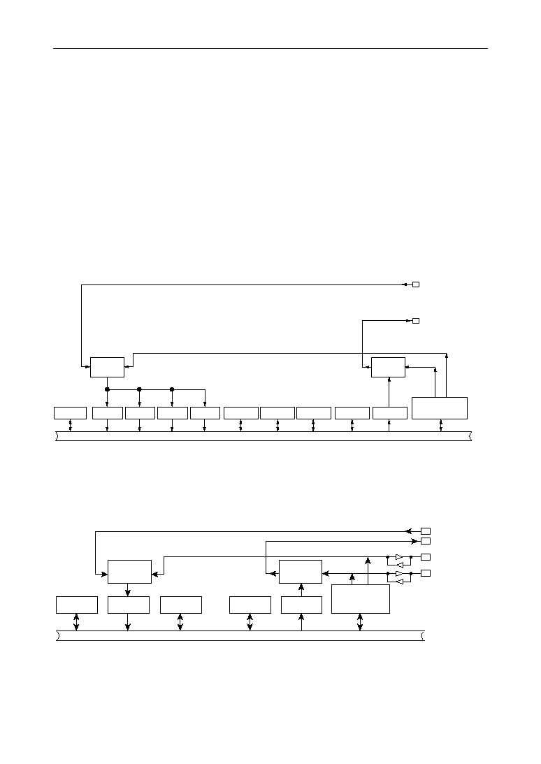
15-2
MSM66591/ML66592 User's Manual
Chapter 15 Serial Port Functions
15.1 Configuration of Serial Ports
SCI0, SCI1, SCI2, SCI3, and SCI4 have the same basic configuration. They consist of:
∑ baud rate generators to control the transfer speed (S0TM, S1TM, S2TM, S3TM,
S4TM: see Chapter 14)
∑ control registers to control transmit/receive operations (SR0CON, SR1CON,
SR2CON, SR3CON, SR4CON, ST0CON, ST1CON, ST2CON, ST3CON, ST4CON)
∑ buffer registers to set transmit/receive data (S0BUFm, S1BUF, S2BUFm, S3BUFm,
S4BUFm: m = 0≠3)
∑ status registers (S0STATm, S1STAT, S2STATm, S3STATm, S4STATm: m = 0≠2)
∑ a transmit register and a receive register
Figure 15-1 shows the configuration of SCI0, SCI2, SCI3, and SCI4. Figure 15-2 shows
the configuration of SCI1. Table 15-2 lists the serial port control SFRs.
TXDn (n = 0: P6_7)
(n = 2: P9_1)
(n = 3: P9_3)
(n = 4: P9_5)
RXDn (n = 0: P6_6)
(n = 2: P9_0)
(n = 3: P9_2)
(n = 4: P9_4)
SRnCON
SnBUF0
SnSTAT0
STnCON SnBUF0
SnTM
8-Bit Timer
Receive
Register
SnBUF1 SnBUF2 SnBUF3
SnSTAT1 SnSTAT2
n = 0, 1, 2, 3, 4
Internal Bus
Transmit
Register
Figure 15-1 Configuration of SCIn (n = 0, 2, 3, 4)
TXD1 (P6_3)
Internal Bus
RXD1 (P6_2)
SR1CON
S1BUF
S1STAT
ST1CON
S1BUF
S1TM
8-Bit Timer
Transmit
Register
Receive
Register
TXC1 (P6_5)
RXC1 (P6_4)
Figure 15-2 Configuration of SCI1
15-3
15
MSM66591/ML66592 User's Manual
Chapter 15 Serial Port Functions
Table 15-2 Serial Port Control SFRs
0028
SCI0 Transmit/Receive Buffer Register 0
S0BUF0
0029
SCI0 Receive Buffer Register 1
S0BUF1
0026
SCI1 Transmit/Receive Buffer Register
S1BUF
0027
SCI1 Status Register
S1STAT
002C
SCI2 Transmit/Receive Buffer Register 0
S2BUF0
002D
SCI2 Receive Buffer Register 1
S2BUF1
R/W
Undefined
Undefined
00
Undefined
8
--
--
--
--
002A
SCI0 Receive Buffer Register 2
S0BUF2
002B
SCI0 Receive Buffer Register 3
S0BUF3
Undefined
--
--
--
--
Undefined
Undefined
Undefined
002E
SCI2 Receive Buffer Register 2
S2BUF2
Undefined
--
002F
SCI2 Receive Buffer Register 3
S2BUF3
Undefined
--
0030
SCI3 Transmit/Receive Buffer Register 0
S3BUF0
Undefined
--
0031
SCI3 Receive Buffer Register 1
S3BUF1
Undefined
--
0032
SCI3 Receive Buffer Register 2
S3BUF2
Undefined
--
0033
SCI3 Receive Buffer Register 3
S3BUF3
Undefined
--
0034
SCI4 Transmit/Receive Buffer Register 0
S4BUF0
Undefined
--
0035
SCI4 Receive Buffer Register 1
S4BUF1
Undefined
--
0036
SCI4 Receive Buffer Register 2
S4BUF2
Undefined
--
0037
SCI4 Receive Buffer Register 3
S4BUF3
Undefined
--
0038
SCI0 Status Register 0
S0STAT0
00
--
0039
SCI0 Interrupt Control Register
SR0INT
01
--
003A
SCI2 Status Register 0
S3STAT0
00
--
003B
SCI2 Interrupt Control Register
SR3INT
01
--
003C
SCI3 Status Register 0
S4STAT0
00
--
003D
SCI3 Interrupt Control Register
SR4INT
01
--
003E
SCI4 Status Register 0
ST0CON
00
--
003F
SCI4 Interrupt Control Register
ST1CON
01
--
0130
SCI0 Transmit Control Register
ST2CON
8A
--
0131
SCI1 Transmit Control Register
ST3CON
88
--
0132
SCI2 Transmit Control Register
ST4CON
8A
--
0133
SCI3 Transmit Control Register
SR0CON
8A
--
0134
SCI4 Transmit Control Register
SR1CON
8A
--
0138
SCI0 Receive Control Register
SR2CON
12
--
0139
SCI1 Receive Control Register
SR3CON
08
--
013A
SCI2 Receive Control Register
SR4CON
12
--
013B
SCI3 Receive Control Register
12
--
013C
SCI4 Receive Control Register
12
--
R
R/W
R
R/W
R
R/W
R
R/W
S2STAT0
SR2INT
8/16-Bit
Operation
Address [H]
Name
Abbreviated
Name (BYTE)
Abbreviated
Name (WORD)
R/W
Reset
State [H]
Some addresses are not consecutive.
Addresses in the address column marked by "" indicate that the register has bits missing.
15-4
MSM66591/ML66592 User's Manual
Chapter 15 Serial Port Functions
Table 15-2 Serial Port Control SFRs (continued)
0190
SCI0 Status Register 1
S2STAT1
11
--
0191
SCI0 Status Register 2
S2STAT2
C1
--
0192
SCI2 Status Register 1
S3STAT1
11
--
0193
SCI2 Status Register 2
S3STAT2
C1
--
0194
SCI3 Status Register 1
S4STAT1
--
0195
SCI3 Status Register 2
S4STAT2
--
0196
SCI4 Status Register 1
--
0197
SCI4 Status Register 2
--
11
C1
11
C1
S0STAT1
S0STAT2
R/W
8
8/16-Bit
Operation
Some addresses are not consecutive.
Addresses in the address column marked by "" indicate that the register has bits missing.
Address [H]
Name
Abbreviated
Name (BYTE)
Abbreviated
Name (WORD)
R/W
Reset
State [H]

15-5
15
MSM66591/ML66592 User's Manual
Chapter 15 Serial Port Functions
15.2 Serial Port Control Registers
15.2.1 Control Registers for SCI0
[1]
SCI0 Transmit Control Register (ST0CON)
ST0CON is a 5-bit register that controls SCI0 transmit operations.
At reset (when the
RES
signal is input, the BRK instruction is executed, the watchdog
timer is overflown, or an operation code trap is generated), ST0CON becomes 8AH, the
SCI0 transmit operation is in UART normal mode, at 8-bit data length, 2 stop bits, and
no parity.
When changing the contents of ST0CON, do so after transmission is completed. If
ST0CON is changed before a transmission is completed, the current and future trans-
mission is not normally performed.
The 4-stage buffer mode is not provided for the transmit side.
Figure 15-3 shows the configuration of ST0CON.
<Description of Each Bit>
∑ ST0MD (bit 0)
This bit specifies the transmit operation mode of SCI0.
∑ ST0MPC (bit 2)
If SCI0 transmits in UART multiprocessor communication mode, this bit specifies
which is transmitted, data or an address. The transmit data length is 8 bits. If this bit
is "0", data is transmitted, and if "1", an address is transmitted.
∑ ST0STB (bit 4)
This bit specifies the stop bit of SCI0 to either 1 stop bit or 2 stop bits. If this bit is "0",
SCI0 transmits at 2 stop bits, and if "1", SCI0 transmits at 1 stop bit.
∑ ST0PEN (bit 5)
This bit specifies whether a parity bit is included when SCI0 transmits. If this bit is
"0", SCI0 transmits without a parity bit, and if "1", SCI0 transmits with a parity bit.
∑ ST0EVN (bit 6)
This bit specifies the logic of the parity bit when SCI0 transmits. If this bit is "0", an
odd parity is selected, and if "1", an even parity is selected.
15-6
MSM66591/ML66592 User's Manual
Chapter 15 Serial Port Functions
Figure 15-3 Configuration of ST0CON
--
ST0EVN ST0PEN ST0STB
--
ST0MPC
--
ST0MD
7
6
5
4
3
2
1
0
"--" indicates a bit that is not provided.
"1" is read if a read instruction is executed.
0 SCI0 UART normal mode
1
SCI0 UART multiprocessor communication mode
0 Data transmitted
1 Address transmitted
0 2 stop bits
1 1 stop bit
Multiprocessor
communication
mode
Parity bit: no
Parity bit: yes
Odd parity
Even parity
0
1
0
1
ST0CON

15-7
15
MSM66591/ML66592 User's Manual
Chapter 15 Serial Port Functions
[2]
SCI0 Receive Control Register (SR0CON)
SR0CON is a 5-bit register that controls SCI0 receive operations.
At reset (when the
RES
signal is input, the BRK instruction is executed, the watchdog
timer is overflown, or an operation code trap is generated), SR0CON becomes 12H, the
SCI0 operation is in UART normal mode, at 8-bit data length, no parity, and receive is
disabled.
When changing the contents of SR0CON, do so after resetting SR0REN (bit 7) to "0". If
the SR0CON is changed before resetting SR0REN (bit 7) to "0", the current and future
receive is not normally performed.
Figure 15-4 shows the configuration of SR0CON.
<Description of Each Bit>
∑ SR0MD (bit 0)
This bit specifies the receive operation mode of SCI0.
∑ SR0MPC (bit 2)
If SCI0 receives in UART multiprocessor communication mode, this bit specifies
which is received, data or an address. The receive data length is 8 bits. If this bit is
"0", data is received, and if "1", an address is received.
∑ SR0EXP (bit 3)
This bit specifies the SCI0 receive buffer mode. If this bit is "0", only S0BUF0 is
enabled as a receive buffer (single buffer mode), and if "1", S0BUF0, S0BUF1,
S0BUF2, and S0BUF3 are enabled as a receive buffer (4-stage buffer mode).
During the 4-stage buffer mode, the receive buffers operate as a ring buffer.
∑ SR0PEN (bit 5)
This bit specifies whether a parity bit is included when SCI0 receives. If this bit is "0",
SCI0 receives without a parity bit, and if "1", SCI0 receives with a parity bit.
∑ SR0EVN (bit 6)
This bit specifies the logic of the parity bit when SCI0 receives. If this bit is "0", SCI0
receives at odd parity, and if "1", SCI0 receives at even parity.
∑ SR0REN (bit 7)
This bit specifies enable/disable of SCI0 receive. If this bit is "0", SCI0 receive is
disabled, and if "1", SCI0 receive is enabled.
15-8
MSM66591/ML66592 User's Manual
Chapter 15 Serial Port Functions
Figure 15-4 Configuration of SR0CON
SR0REN SR0EVN SR0PEN
--
SR0EXP SR0MPC
--
SR0MD
7
6
5
4
3
2
1
0
"--" indicates a bit that is not provided.
"1" is read if a read instruction is executed.
0 SCI0 UART normal mode
1
SCI0 UART multiprocessor communication mode
0 Data is received
1 Address is received
0
1
0
1
0
1
Multiprocessor
communication
mode
Parity bit: no
Parity bit: yes
Odd parity
Even parity
SCI0 receive disabled
SCI0 receive enabled
SR0CON
0 Single buffer mode
1 4-stage buffer mode (receive side)

15-9
15
MSM66591/ML66592 User's Manual
Chapter 15 Serial Port Functions
[3]
SCI0 Transmit/Receive Buffer Register (S0BUF0)
S0BUF0 is an 8-bit register that holds transmit/receive data during a serial port transmit/
receive operation. S0BUF0 has a double structure, in which the contents are different in
read/write. If in read, S0BUF0 functions as a receive buffer, and if in write, S0BUF0
functions as a transmit buffer.
When a receive operation ends, the content of the receive register is transferred to the
S0BUF0 receive buffer, and a receive interrupt request is generated at the same time.
The content of the S0BUF0 receive buffer is held until the next receive operation ends.
When receive mode is in UART multiprocessor communication mode, and if receive
data is ignored, the content of S0BUF0 is not updated even at completion of the receive
operation, and a receive interrupt request is not generated.
At reset (when the
RES
signal is input, the BRK instruction is executed, the watchdog
timer is overflown, or an operation code trap is generated), S0BUF0 becomes unde-
fined.
[4]
SCI0 Receive Buffer Registers (S0BUF1, S0BUF2, S0BUF3)
S0BUF1, S0BUF2, and S0BUF3 are 8-bit registers that store valid received data when
the SR0EXP bit of SR0CON is set to "1" (4-stage buffer mode).
These registers are read-only and cannot be written to. During the 4-stage buffer mode,
at the completion of each 1-byte reception, the contents of the receive register are
transferred to a receive buffer register in the order of S0BUF0, S0BUF1, S0BUF2,
S0BUF3, S0BUF0, etc. At the same time, a receive interrupt request is generated.
(Ring Buffer Type)
When the receive mode is the UART multiprocessor communication mode and the
received data is ignored, the contents of S0BUF1, S0BUF2, and S0BUF3 will not be
updated and a receive interrupt request will not be generated even after completion of a
receive operation.
At reset (when the
RES
signal is input, the BRK instruction is executed, the watchdog
timer is overflown, or an operation code trap is generated), the contents of S0BUF1,
S0BUF2, and S0BUF3 are undefined.
[5]
SCI0 Transmit and Receive Registers
The SCI0 transmit and receive registers are two 8-bit shift registers that actually per-
form shift operations during a transmit/receive operation.
The transmit and receive registers and the transmit/receive buffer registers have a
double structure. If a receive operation ends, during single buffer mode the data re-
ceived by the receive register is transferred to S0BUF0, and during 4-stage buffer mode
it is transferred to S0BUF0, S0BUF1, S0BUF2, and S0BUF3 in this order, and a receive
interrupt request is generated.
The transmit and receive registers cannot be read/written by the program.

15-10
MSM66591/ML66592 User's Manual
Chapter 15 Serial Port Functions
[6]
SCI0 Status Register 0 (S0STAT0)
The high-order 4 bits of S0STAT0 is the transmit-ready/receive-ready interrupt request
control register of the serial port. The low-order 4 bits of S0STAT0 is the register that
holds the status (normal/abnormal) when the serial port receive operation is completed.
The low-order 4 bits of S0STAT0 are updated when receive ends. Once S0STAT0 is
set to "1" ("1": error occurred), it is not reset to "0" even if an error does not occur when
the next receive ends. Therefore reset to "0" any bits that are "1" of the low-order 4 bits
of S0STAT0 by the program when a receive ends.
The contents of S0BUF0 must be read before resetting OERR00 (bit 1) of the low-order
4 bits of S0STAT0. Otherwise, the OERR00 flag is set to "1" again irrespective of
occurrence of an overrun error in next receive operation.
During the 4-stage buffer mode, an overrun error flag, parity error flag, and multi-
processor communication flag are provided for each buffer. However, with a 4-stage
buffer, only 1 bit is provided for the framing error flag. Therefore, the framing error flag
will be set at the time when even 1 byte of the received data has a framing error.
At reset (when the
RES
signal is input, the BRK instruction is executed, the watchdog
timer is overflown, or an operation code trap is generated), S0STAT0 becomes 00H.
Figure 15-5 shows the configuration of S0STAT0.

15-11
15
MSM66591/ML66592 User's Manual
Chapter 15 Serial Port Functions
<Description of Each Bit>
∑ FERR0 (bit 0)
If the stop bit received by SCI0 is "0", this bit is set to "1" interpreting that frame
synchronization is incorrect. (Framing error)
∑ OERR00 (bit 1)
This bit is set to "1" if the data transferred to S0BUF0 for the previous reception has
not yet been read by the CPU when the receive operation of SCI0 ends. However,
new receive data is loaded to S0BUF0 even if this occurs. (Overrun error)
∑ PERR00 (bit 2)
The parity of data received by SCI0 and the parity bit appended to and transferred
with data are compared, and if they do not match, this bit is set to "1". (Parity error)
∑ MERR00 (bit 3)
This bit is set to "1" if an address is sent while receiving data in SCI0 UART multi-
processor communication mode. This means that if the MPC bit (of the data that is
transferred when the SR0MPC bit of SR0CON is "0") is "1", MERR00 is set, inter-
preting this as a multiprocessor communication error.
∑ RV0IE0 (bit 4)
This bit enables/disables the generation of an SCI0 receive ready interrupt request. If
this bit is "1", generation is enabled, and if "0", generation is disabled.
∑ RV0IRQ0 (bit 5)
This bit is set to "1" if an SCI0 receive ready is generated. This bit is not automati-
cally reset to "0" even if an interrupt process is executed, therefore set it to "0" by the
program.
∑ TR0IE (bit 6)
This bit enables/disables the generation of an SCI0 transmit ready interrupt request.
If this bit is "1", generation is enabled, and if "0", generation is disabled.
∑ TR0IRQ (bit 7)
This bit is set to "1" if an SCI0 transmit ready is generated. This bit is not automati-
cally reset to "0" even if an interrupt process is executed, therefore set it to "0" by the
program.
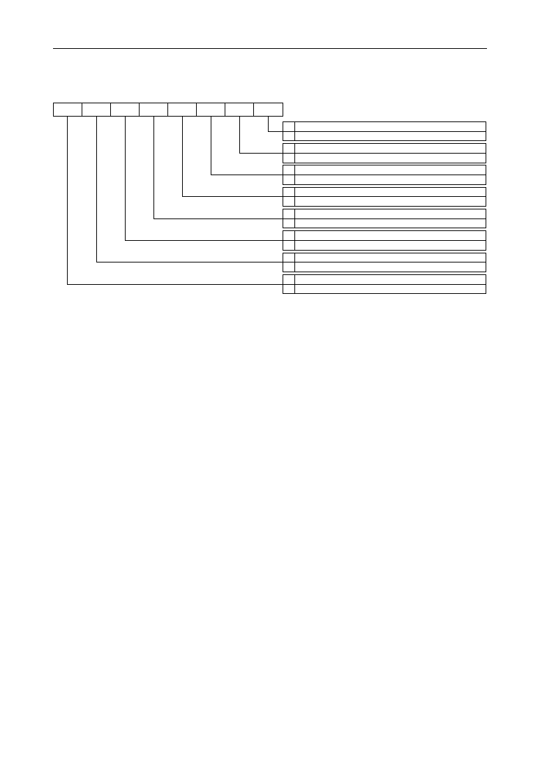
15-12
MSM66591/ML66592 User's Manual
Chapter 15 Serial Port Functions
Figure 15-5 Configuration of S0STAT0
TR0IRQ TR0IE RV0IRQ0 RV0IE0 MERR00 PERR00 OERR00 FERR0
7
6
5
4
3
2
1
0
0 SCI0 framing error:no
1 SCI0 framing error:yes
0 S0BUF0 overrun error:no
1 S0BUF0 overrun error:yes
0 S0BUF0 parity error:no
1 S0BUF0 parity error:yes
0
S0BUF0 multiprocessor communication error:no
1
S0BUF0 multiprocessor communication error:yes
0
S0BUF0 receive ready interrupt request generation:disabled
1
S0BUF0 receive ready interrupt request generation:enabled
0 S0BUF0 receive ready generation:no
1 S0BUF0 receive ready generation:yes
0 SCI0 transmit ready interrupt request generation:disabled
1 SCI0 transmit ready interrupt request generation:enabled
0 SCI0 transmit ready generation:no
1 SCI0 transmit ready generation:yes
S0STAT0

15-13
15
MSM66591/ML66592 User's Manual
Chapter 15 Serial Port Functions
[7]
SCI0 Status Register 1 (S0STAT1)
If the SR0EXP bit of SR0CON is set to "1" (4-stage buffer mode), the 6-bit S0STAT1
register stores the status (normal/abnormal) of the serial transfer when a serial port
receive operation is completed.
During the 4-stage buffer mode, if there is an error in the receive data transferred to
S0BUF1, the lower 3 bits of S0STAT1 (bits 1≠3) are updated when reception of that
data is complete; if there is an error in the receive data transferred to S0BUF2, the
upper 3 bits of S0STAT1 (bits 5≠7) are updated when reception of that data is com-
plete. Once S0STAT1 is set to "1" ("1": error occurred), it is not reset to "0" even if that
error has not occurred at completion of the next reception. Therefore, with the program,
reset to "0" any S0STAT1 bits that are "1" after reception is complete. Read the con-
tents of S0BUF1 and S0BUF2 before resetting the OERR01 and OERR02 flags in
S0STAT1. If the contents of S0BUF1 and S0BUF2 are not read, the OERR01 and
OERR02 flags will be set to "1" again regardless of whether an overrun error occurs in
the next receive operation.
At reset (when the
RES
signal is input, the BRK instruction is executed, the watchdog
timer is overflown, or an operation code trap is generated), S0STAT1 becomes 11H.
Figure 15-6 shows the configuration of S0STAT1.
<Description of Each Bit>
∑ OERR01 (bit 1)
When an SCI0 receive operation is complete and the receive data is transferred into
S0BUF1, OERR01 is set to "1" if the data transferred into S0BUF1 for the previous
reception has not yet been read by the CPU. New receive data is loaded into
S0BUF1 even if OERR01 has been set. (Overrun error)
∑ PERR01 (bit 2)
With SCI0, the parity of data received by S0BUF1 is compared to the parity bit
appended to and transferred with the data. If they do not match, PERR01 is set to
"1". (Parity error)
∑ MERR01 (bit 3)
During the SCI0 UART multiprocessor communication mode, MERR01 is set to "1" if
an address is transmitted while S0BUF1 is receiving data. In other words, when the
MPC bit (of the data that is transferred when the SR0MPC bit of SR0CON is "0") is
"1", MERR01 is set to "1", interpreting this as a multiprocessor communication error.
∑ OERR02 (bit 5)
When an SCI0 receive operation is complete and the receive data is transferred into
S0BUF2, OERR02 is set to "1" if the data transferred into S0BUF2 for the previous
reception has not yet been read by the CPU. New receive data is loaded into
S0BUF2 even if OERR02 has been set. (Overrun error)
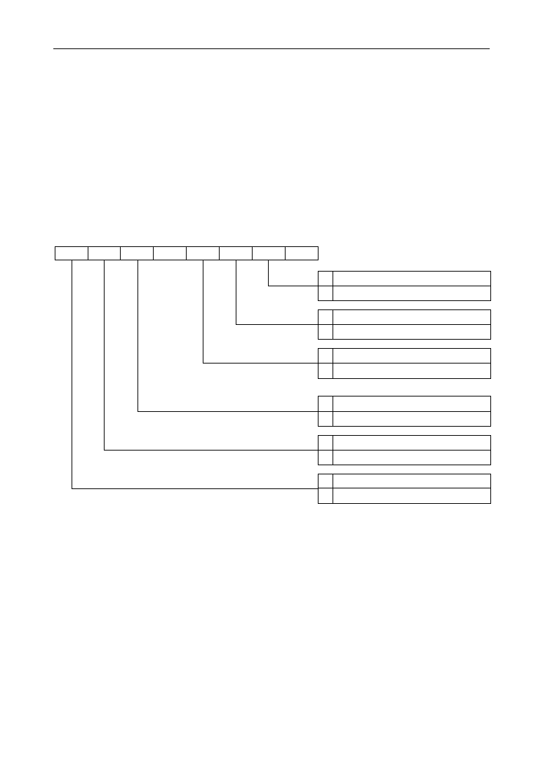
15-14
MSM66591/ML66592 User's Manual
Chapter 15 Serial Port Functions
∑ PERR02 (bit 6)
With SCI0, the parity of data received by S0BUF2 is compared to the parity bit
appended to and transferred with the data. If they do not match, PERR02 is set to
"1". (Parity error)
∑ MERR02 (bit 7)
During the SCI0 UART multiprocessor communication mode, MERR02 is set to "1" if
an address is transmitted while S0BUF2 is receiving data. In other words, when the
MPC bit (of the data that is transferred when the SR0MPC bit of SR0CON is "0") is
"1", MERR02 is set to "1", interpreting this as a multiprocessor communication error.
Figure 15-6 Configuration of S0STAT1
7
MERR02
6
PERR02
5
OERR02
4
--
3
MERR01
2
PERR01
1
OERR01
0
--
0
1
S0BUF1 overrun error: no
S0BUF1 overrun error: yes
0
1
0
1
S0BUF1 multiprocessor communication error: no
S0BUF1 multiprocessor communication error: yes
S0BUF1 parity error: no
S0BUF1 parity error: yes
0
1
S0BUF2 overrun error: no
S0BUF2 overrun error: yes
0
1
0
1
S0BUF2 multiprocessor communication error: no
S0BUF2 multiprocessor communication error: yes
S0BUF2 parity error: no
S0BUF2 parity error: yes
"--" indicates a bit that is not provided.
"1" is read if a read instruction is executed.
S0STAT1

15-15
15
MSM66591/ML66592 User's Manual
Chapter 15 Serial Port Functions
[8]
SCI0 Status Register 2 (S0STAT2)
If the SR0EXP bit of SR0CON is set to "1" (4-stage buffer mode), the lower 3 bits of
S0STAT2 store the status (normal/abnormal) of the serial transfer when a serial port
receive operation is completed. The upper 2 bits of S0STAT2 monitor the counter that
indicates the receive buffer into which receive data will be transferred at completion of
the next receive operation.
During the 4-stage buffer mode, if there is an error in the receive data transferred to
S0BUF3, the lower 3 bits of S0STAT2 (bits 1≠3) are updated when reception of that
data is complete. Once the lower 3 bits of S0STAT2 are set to "1" ("1": error occurred),
they are not reset to "0" even if that error has not occurred at completion of the next
reception. Therefore, with the program, reset to "0" any bits that are "1" of the lower 3
bits of S0STAT2 after reception is complete. Read the contents of S0BUF3 before
resetting the OERR03 flag in the lower 3 bits of S0STAT2. If the contents of S0BUF3
are not read, the OERR03 flag will be set to "1" again regardless of whether an overrun
error occurs in the next receive operation.
Bits 4 and 5 of S0STAT2 are read-only and cannot be written to. During the 4-stage
buffer mode, the next receive buffer into which data will be transferred (S0BUF0,
S0BUF1, S0BUF2, S0BUF3) can be verified by reading bits 4 and 5 of S0STAT2.
At reset (when the
RES
signal is input, the BRK instruction is executed, the watchdog
timer is overflown, or an operation code trap is generated), S0STAT2 becomes C1H.
Figure 15-7 shows the configuration of S0STAT2.
<Description of Each Bit>
∑ OERR03 (bit 1)
When an SCI0 receive operation is complete and the receive data is transferred into
S0BUF3, OERR03 is set to "1" if the data transferred into S0BUF3 for the previous
reception has not yet been read by the CPU. New receive data is loaded into
S0BUF3 even if OERR03 has been set. (Overrun error)
∑ PERR03 (bit 2)
With SCI0, the parity of data received by S0BUF3 is compared to the parity bit
appended to and transferred with the data. If they do not match, PERR03 is set to
"1". (Parity error)
∑ MERR03 (bit 3)
During the SCI0 UART multiprocessor communication mode, MERR03 is set to "1" if
an address is transmitted while S0BUF3 is receiving data. In other words, when the
MPC bit (of the data that is transferred when the SR0MPC bit of SR0CON is "0") is
"1", MERR03 is set to "1", interpreting this as a multiprocessor communication error.
∑ BFCU00 (bit 4), BFCU01 (bit 5)
During the 4-stage buffer mode, BFCU00 and BFCU01 monitor the buffer counter
that indicates the receive buffer into which receive data will be transferred (S0BUF0,
S0BUF1, S0BUF2, S0BUF3) at completion of the next receive operation. BFCU00
and BFCU01 are read-only and cannot be written to.
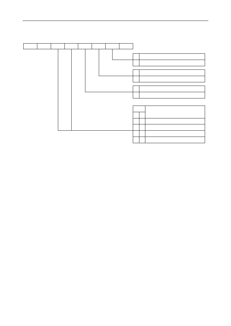
15-16
MSM66591/ML66592 User's Manual
Chapter 15 Serial Port Functions
Figure 15-7 Configuration of S0STAT2
7
--
6
--
5
BFCU01
4
BFCU00
3
MERR03
2
PERR03
1
OERR03
0
--
0
1
S0BUF3 overrun error: no
S0BUF3 overrun error: yes
0
1
0
1
S0BUF3 multiprocessor communication error: no
S0BUF3 multiprocessor communication error: yes
S0BUF3 parity error: no
S0BUF3 parity error: yes
BFCU0
1
Buffer counter monitor during SCI0
4-stage buffer mode
"--" indicates a bit that is not provided.
"1" is read if a read instruction is executed.
0
0
0
0
1
1
0
1
1
Write to S0BUF0 next
Write to S0BUF1 next
Write to S0BUF2 next
Write to S0BUF3 next
S0STAT2

15-17
15
MSM66591/ML66592 User's Manual
Chapter 15 Serial Port Functions
[9]
SCI0 Interrupt Control Register (SR0INT)
When SCI0 is in the 4-stage buffer mode (SR0EXP bit of SR0CON is "1"), the 7-bit
SR0INT register controls the receive-ready interrupt requests for each receive buffer
(S0BUF0 to S0BUF3).
At reset (when the
RES
signal is input, the BRK instruction is executed, the watchdog
timer is overflown, or an operation code trap is generated), SR0INT becomes 01H.
RV0IRQ0 (bit 4) of SR0INT monitors RV0IRQ0 (bit 3) of S0STAT0. During the 4-stage
buffer mode, by reading SR0INT once, it is possible to verify which buffer has generated
a receive-ready. This bit is read-only and writes are ignored. To clear (write to) this bit,
write to RV0IRQ0 (bit 5) of S0STAT0.
Figure 15-8 shows the configuration of SR0INT.
<Description of Each Bit>
∑ RV0IE1 (bit 1)
This bit enables or disables the generation of SCI0 S0BUF1 receive-ready interrupt
requests. If this bit is "1", generation is enabled, and if "0", generation is disabled.
∑ RV0IE2 (bit 2)
This bit enables or disables the generation of SCI0 S0BUF2 receive-ready interrupt
requests. If this bit is "1", generation is enabled, and if "0", generation is disabled.
∑ RV0IE3 (bit 3)
This bit enables or disables the generation of SCI0 S0BUF3 receive-ready interrupt
requests. If this bit is "1", generation is enabled, and if "0", generation is disabled.
∑ RV0IRQ0 (bit 4)
This bit monitors RV0IRQ0 of S0STAT0. (Read-only)
This bit is set to "1" when an SCI0 S0BUF0 receive-ready is generated. To clear this
bit to "0", clear RV0IRQ0 of S0STAT0.
∑ RV0IRQ1 (bit 5)
This bit is set to "1" when an SCI0 S0BUF1 receive-ready is generated. This bit is not
automatically cleared to "0" even when an SCI0 interrupt is processed, so clear it by
the program.
∑ RV0IRQ2 (bit 6)
This bit is set to "1" when an SCI0 S0BUF2 receive-ready is generated. This bit is not
automatically cleared to "0" even when an SCI0 interrupt is processed, so clear it by
the program.
∑ RV0IRQ3 (bit 7)
This bit is set to "1" when an SCI0 S0BUF3 receive-ready is generated. This bit is not
automatically cleared to "0" even when an SCI0 interrupt is processed, so clear it by
the program.
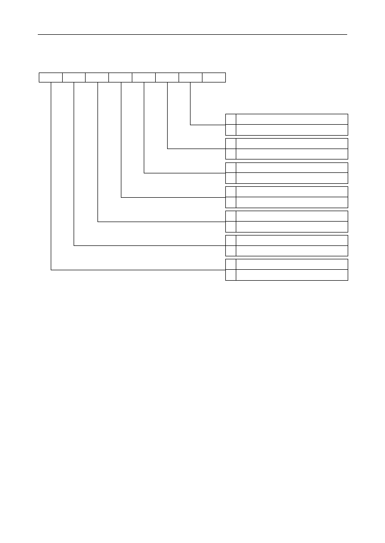
15-18
MSM66591/ML66592 User's Manual
Chapter 15 Serial Port Functions
Figure 15-8 Configuration of SR0INT
7
RV0IRQ3
6
RV0IRQ2
5
RV0IRQ1
4
RV0IRQ0
3
RV0IE3
2
RV0IE2
1
RV0IE1
0
--
0
1
S0BUF1 receive-ready interrupt request generation: disabled
S0BUF1 receive-ready interrupt request generation: enabled
0
1
S0BUF2 receive-ready interrupt request generation: disabled
S0BUF2 receive-ready interrupt request generation: enabled
0
1
S0BUF3 receive-ready interrupt request generation: disabled
S0BUF3 receive-ready interrupt request generation: enabled
0
1
S0BUF0 receive-ready generation: no (see note)
S0BUF0 receive-ready generation: yes (see note)
0
1
S0BUF1 receive-ready generation: no
S0BUF1 receive-ready generation: yes
0
1
S0BUF2 receive-ready generation: no
S0BUF2 receive-ready generation: yes
0
1
S0BUF3 receive-ready generation: no
S0BUF3 receive-ready generation: yes
[Note]
RV0IRQ0 is read-only. To clear, write to the
RV0IRQ0 bit of S0STAT0.
"--" indicates a bit that is not provided.
"1" is read if a read instruction is executed.
SR0INT

15-19
15
MSM66591/ML66592 User's Manual
Chapter 15 Serial Port Functions
15.2.2 Control Registers for SCI1
[1]
SCI1 Transmit Control Register (ST1CON)
ST1CON is a 6-bit register that controls SCI1 transmit operations.
At reset (when the
RES
signal is input, the BRK instruction is executed, the watchdog
timer is overflown, or an operation code trap is generated), ST1CON becomes 88H, the
SCI1 transmit operation is in UART normal mode, at 8-bit data length, 2 stop bits, and
no parity.
When changing the contents of ST1CON, do so after transmission is completed. If
ST1CON is changed before a transmission is completed, the current and future trans-
mission is not normally performed.
Figure 15-9 shows the configuration of ST1CON.
<Description of Each Bit>
∑ ST1MD0, 1 (bits 0 , 1)
These bits specify the transmit operation mode of SCI1.
∑ ST1MPC (bit 2)
If SCI1 transmits in UART/synchronous multiprocessor communication mode, bit 2
(ST1MPC) specifies which is transmitted, data or an address. The transmit data
length is fixed at 8 bits. If bit 2 (ST1MPC) is "0", data is transmitted, and if "1", an
address is transmitted.
∑ ST1STB/ST1MST (bit 4)
The function of bit 4 differs depending on the operation mode specified by bit 1 and
0. When SCI1 transmits in UART mode, bit 4 (ST1STB) specifies the stop bit of SCI1
either as a 1 stop bit or 2 stop bits. If bit 4 (ST1STB) is "0", SCI1 transmits at 2 stop
bits, and if "1", SCI1 transmits at 1 stop bit. When SCI1 transmits in synchronous
mode, bit 4 (ST1MST) selects slave mode/master mode. If bit 4 (ST1MST) is "0",
slave mode is selected, and if "1", master mode is selected.
∑ ST1PEN (bit 5)
This bit specifies whether a parity bit is included when SCI1 transmits. If this bit is
"0", SCI1 transmits without a parity bit, and if "1", SCI1 transmits with a parity bit.
∑ ST1EVN (bit 6)
This bit specifies the logic of a parity bit when SCI1 transmits. If this bit is "0", SCI1
transmits at odd parity, and if "1", SCI1 transmits at even parity.
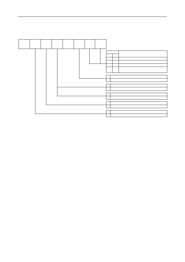
15-20
MSM66591/ML66592 User's Manual
Chapter 15 Serial Port Functions
Figure 15-9 Configuration of ST1CON
--
ST1EVN ST1PEN
ST1STB
ST1MST
--
ST1MPC ST1MD1 ST1MD0
7
6
5
4
3
2
1
0
Multiprocessor
communication
mode (ST1MPC)
UART mode
(ST1STB)
Synchronous
mode
(ST1MST)
"--" indicates a bit that is not provided.
"1" is read if a read instruction is executed.
ST1MD
SCI1 Transmit Operation Mode
1
0
0
0 UART normal mode
0
1
UART multiprocessor communication mode
1
0 Synchronous normal mode
1
1
Synchronous multiprocessor
communication mode
0 Data transmit
1 Address transmit
0 2 stop bits
1 1 stop bit
0 Transmit in slave mode
1 Transmit in master mode
0 Parity bit: no
1 Parity bit: yes
0 Odd parity
1 Even parity
ST1CON

15-21
15
MSM66591/ML66592 User's Manual
Chapter 15 Serial Port Functions
[2]
SCI1 Receive Control Register (SR1CON)
SR1CON is 7-bit register that controls the SCI1 receive operations.
At reset (when the
RES
signal is input, the BRK instruction is executed, the watchdog
timer is overflown, or an operation code trap is generated), SR1CON becomes 08H, the
SCI1 receive operation is in UART normal mode, at 8-bit data length, no parity, and
receive is disabled.
When changing the contents of SR1CON, do so after resetting SR1REN (bit 7) to "0". If
SR1CON is changed before resetting SR1REN to "0", the current and future receive is
not normally performed.
Figure 15-10 shows the configuration of SR1CON.
<Description of Each Bit>
∑ SR1MD0, 1 (bits 0, 1)
These two bits specify the receive operation mode of SCI1.
∑ SR1MPC (bit 2)
If SCI1 receives in UART/synchronous multiprocessor communication mode, bit 2
(SR1MPC) specifies which is received, data or an address. The receive data is 8-bit
data length.
If bit 2 (SR1MPC) is "0", data is received, and if "1", an address is received.
∑ SR1MST (bit 4)
The function of bit 4 differs depending on the operation mode specified by bits 1 and
0. When SCI1 receives in UART mode, bit 4 is meaningless. When SCI1 receives in
synchronous mode, slave mode is selected if bit 4 is "0", and master mode is se-
lected if bit 4 is "1".
∑ SR1PEN (bit 5)
This bit specifies whether a parity bit is included when SCI1 receives. If this bit is "0",
SCI1 receives without a parity bit, and if "1", SCI1 receives with a parity bit.
∑ SR1EVN (bit 6)
This bit specifies the logic of a parity bit when SCI1 receives. If this bit is "0", SCI1
receives at odd parity, and if "1", SCI1 receives at even parity.
∑ SR1REN (bit 7)
This bit specifies enable/disable of SCI1 receive. If this bit is "0", SCI1 receive is
disabled, and if "1", SCI1 receive is enabled.
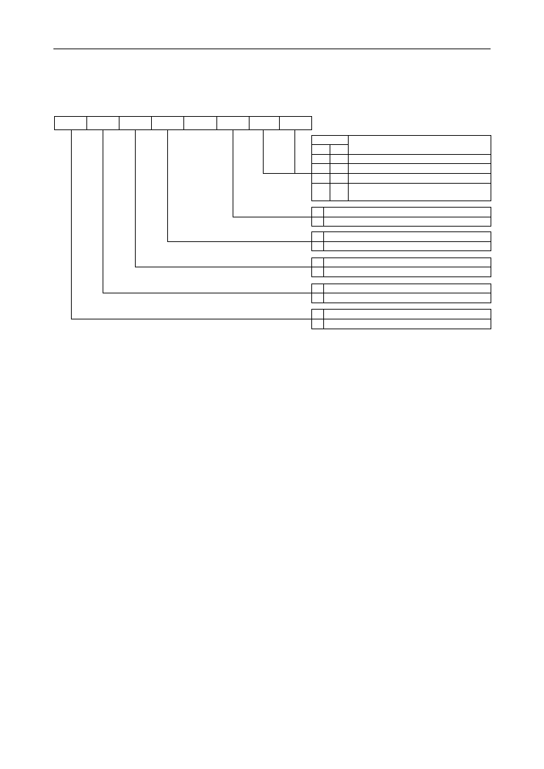
15-22
MSM66591/ML66592 User's Manual
Chapter 15 Serial Port Functions
Figure 15-10 Configuration of SR1CON
SR1REN SR1EVN SR1PEN SR1MST
--
SR1MPC SR1MD1 SR1MD0
7
6
5
4
3
2
1
0
Multiprocessor
communication
mode
"--" indicates a bit that is not provided.
"1" is read if a read instruction is executed.
SR1MD
SCI1 Receive Operation Mode
1
0
0
0 UART normal mode
0
1
UART multi-processor communication mode
1
0 Synchronous normal mode
1
1
Synchronous multiprocessor
communication mode
0 Data receive
1 Address receive
0 Receive in slave mode
1 Receive in master mode
0 Parity bit: no
1 Parity bit: yes
0 Odd parity
1 Even parity
0 SCI1 receive disable
1 SCI1 receive enable
Synchronous mode
SR1CON

15-23
15
MSM66591/ML66592 User's Manual
Chapter 15 Serial Port Functions
[3]
SCI1 Transmit/Receive Buffer Register (S1BUF)
S1BUF is an 8-bit register that holds transmit/receive data during a serial port transmit/
receive operation. S1BUF has a double structure, in which the content is different in
READ/WRITE. If in read, S1BUF functions as a receive buffer, and if in write, S1BUF
functions as a transmit buffer.
When a receive operation ends, the content of the receive register is transferred to the
S1BUF receive buffer, and a receive interrupt request is generated at the same time.
The content of the S1BUF receive buffer is held until the next receive operation ends.
When receive mode is in UART/synchronous multiprocessor communication mode, if
data has been received instead of reception of an address and if the receive data is
ignored, the content of S1BUF is not updated even at completion of the receive opera-
tion, also a receive interrupt request is not generated.
The 4-stage buffer mode is not provided for SCI1.
At reset (when the
RES
signal is input, the BRK instruction is executed, the watchdog
timer is overflown, or an operation code trap is generated), S1BUF becomes undefined.
[4]
SCI1 Transmit and Receive Registers
The SCI1 transmit and receive registers are two 8-bit shift registers that actually per-
form shift operations during a transmit/receive operation.
The transmit and receive registers and transmit/receive buffer register (S1BUF) have a
double structure. When a receive operation ends, the data received by the receive
register is transferred to S1BUF, and a receive interrupt request is generated.
The transmit and receive registers cannot be read/written by the program.
[5]
SCI1 Status Register (S1STAT)
The high-order 4 bits of S1STAT is the transmit-ready/receive-ready interrupt request
control register of the serial port. The low-order 4 bits of S1STAT is the register that
holds the status (normal/abnormal) when the serial port receive operation is completed.
The low-order 4-bits of S1STAT are updated when receive ends. Once S1STAT is set
("1": error occurred), it is not reset to "0" even if an error does not occur when the next
receive ends. Therefore reset to "0" any bits that are "1" of the low-order 4 bits of
S1STAT by the program when a receive ends.
The contents of S1BUF must be read before resetting OERR1 (bit 1) of the low-order 4
bits of S1STAT to "0". Otherwise, the OERR1 flag is set to "1" again irrespective of
occurrence of an overrun error in next receive operation.
At reset (when the
RES
signal is input, the BRK instruction is executed, the watchdog
timer is overflown, or an operation code trap is generated), S1STAT becomes 00H.
Figure 15-11 shows the configuration of S1STAT.

15-24
MSM66591/ML66592 User's Manual
Chapter 15 Serial Port Functions
<Description of Each Bit>
∑ FERR1 (bit 0)
If the stop bit received by SCI1 is "0", this bit is set to "1" interpreting that frame
synchronization is incorrect. (Framming error)
∑ OERR1 (bit 1)
This bit is set to "1" if the previously received data is not read by the CPU when the
receive operation of SCI1 ends. However, new receive data is loaded to S1BUF even
if this occurs. (Overrun error)
∑ PERR1 (bit 2)
The parity of data received by SCI1 and the parity bit appended to and transferred
with data are compared, and if they do not match, this bit is set to "1". (Parity error)
∑ MERR1 (bit 3)
This bit is set to "1" if an address is sent while receiving data in SCI1 UART/synchro-
nous multiprocessor communication mode. This means that if the MPC bit (of the
data that is transferred when the SR1MPC bit of SR1CON is "0") is "1", MERR1 is
set, interpreting this as a multiprocessor communication error.
∑ RV1IE (bit 4)
This bit enables/disables the generation of an SCI1 receive ready interrupt request. If
this bit is "1", generation is enabled, and if "0", generation is disabled.
∑ RV1IRQ (bit 5)
This bit is set to "1" if an SCI1 receive ready is generated. This bit is not automati-
cally reset to "0" even if an interrupt process is executed, therefore set it to "0" by the
program.
∑ TR1IE (bit 6)
This bit enables/disables the generation of an SCI1 transmit ready interrupt request.
If this bit is "1", generation is enabled, and if "0", generation is disabled.
∑ TR1IRQ (bit 7)
This bit is set to "1" if an SCI1 transmit ready is generated. This bit is not automati-
cally reset to "0" even if an interrupt process is executed, therefore set it to "0" by the
program.
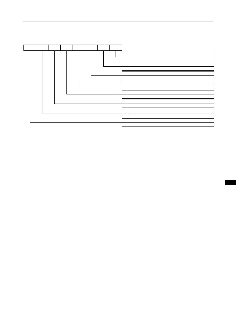
15-25
15
MSM66591/ML66592 User's Manual
Chapter 15 Serial Port Functions
TR1IRQ TR1IE RV1IRQ RV1IE MERR1 PERR1 OERR1 FERR1
7
6
5
4
3
2
1
0
0 SCI1 framing error:no
1 SCI1 framing error:yes
0 SCI1 overrun error:no
1 SCI1 overrun error:yes
0 SCI1 parity error:no
1 SCI1 parity error:yes
0 SCI1 multiprocessor communication error:no
1 SCI1 multiprocessor communication error:yes
0
SCI1 receive ready interrupt request generation:disabled
1
SCI1 receive ready interrupt request generation:enabled
0 SCI1 receive ready generation:no
1 SCI1 receive ready generation:yes
0
SCI1 transmit ready interrupt request generation:disabled
1
SCI1 transmit ready interrupt request generation:enabled
0 SCI1 transmit ready generation:no
1 SCI1 transmit ready generation:yes
S1STAT
Figure 15-11 Configuration of S1STAT

15-26
MSM66591/ML66592 User's Manual
Chapter 15 Serial Port Functions
15.2.3 Control Registers for SCI2
[1]
SCI2 Transmit Control Register (ST2CON)
ST2CON is a 5-bit register that controls SCI2 transmit operations.
At reset (when the
RES
signal is input, the BRK instruction is executed, the watchdog
timer is overflown, or an operation code trap is generated), ST2CON becomes 8AH, the
SCI2 transmit operation is in UART normal mode, at 8-bit data length, 2 stop bits, and
no parity.
When changing the contents of ST2CON, do so after transmission is completed. If
ST2CON is changed before a transmission is completed, the current and future trans-
mission is not normally performed.
The 4-stage buffer mode is not provided for the transmit side.
Figure 15-12 shows the configuration of ST2CON.
<Description of Each Bit>
∑ ST2MD (bit 0)
This bit specifies the transmit operation mode of SCI2.
∑ ST2MPC (bit 2)
If SCI2 transmits in UART multiprocessor communication mode, this bit specifies
which is transmitted, data or an address. The transmit data length is 8 bits. If this bit
is "0", data is transmitted, and if "1", an address is transmitted.
∑ ST2STB (bit 4)
This bit specifies the stop bit of SCI2 to either 1 stop bit or 2 stop bits. If this bit is "0",
SCI2 transmits at 2 stop bits, and if "1", SCI2 transmits at 1 stop bit.
∑ ST2PEN (bit 5)
This bit specifies whether a parity bit is included when SCI2 transmits. If this bit is
"0", SCI2 transmits without a parity bit, and if "1", SCI2 transmits with a parity bit.
∑ ST2EVN (bit 6)
This bit specifies the logic of the parity bit when SCI2 transmits. If this bit is "0", an
odd parity is selected, and if "1", an even parity is selected.
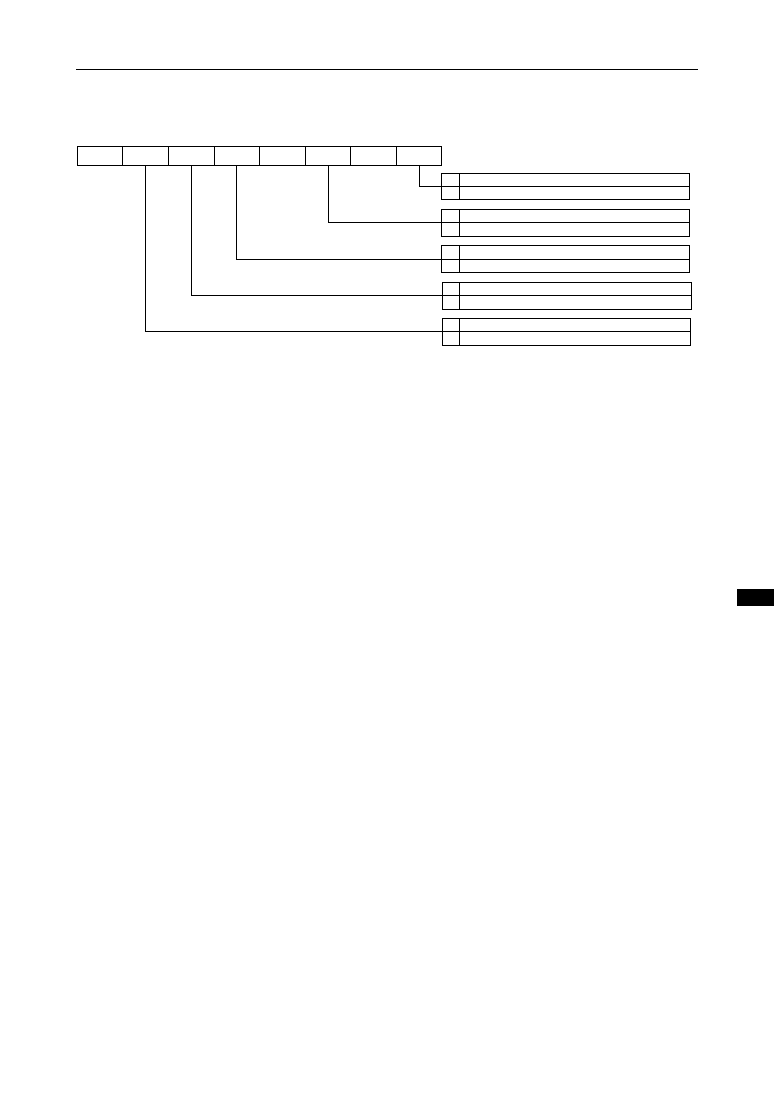
15-27
15
MSM66591/ML66952 User's Manual
Chapter 15 Serial Port Functions
Figure 15-12 Configuration of ST2CON
--
ST2EVN ST2PEN ST2STB
--
ST2MPC
--
ST2MD
7
6
5
4
3
2
1
0
"--" indicates a bit that is not provided.
"1" is read if a read instruction is executed.
0 SCI2 UART normal mode
1
SCI2 UART multiprocessor communication mode
0 Data transmitted
1 Address transmitted
0 2 stop bits
1 1 stop bit
Multiprocessor
communication
mode
Parity bit: no
Parity bit: yes
Odd parity
Even parity
0
1
0
1
ST2CON

15-28
MSM66591/ML66592 User's Manual
Chapter 15 Serial Port Functions
[2]
SCI2 Receive Control Register (SR2CON)
SR2CON is a 5-bit register that controls SCI2 receive operations.
At reset (when the
RES
signal is input, the BRK instruction is executed, the watchdog
timer is overflown, or an operation code trap is generated), SR2CON becomes 12H, the
SCI2 operation is in UART normal mode, at 8-bit data length, no parity, and receive is
disabled.
When changing the contents of SR2CON, do so after resetting SR2REN (bit 7) to "0". If
the SR2CON is changed before resetting SR2REN (bit 7) to "0", the current and future
receive is not normally performed.
Figure 15-13 shows the configuration of SR2CON.
<Description of Each Bit>
∑ SR2MD (bit 0)
This bit specifies the receive operation mode of SCI2.
∑ SR2MPC (bit 2)
If SCI2 receives in UART multiprocessor communication mode, this bit specifies
which is received, data or an address. The receive data length is 8 bits. If this bit is
"0", data is received, and if "1", an address is received.
∑ SR2EXP (bit 3)
This bit specifies the SCI2 receive buffer mode. If this bit is "0", only S2BUF0 is
enabled as a receive buffer (single buffer mode), and if "1", S2BUF0, S2BUF1,
S2BUF2, and S2BUF3 are enabled as a receive buffer (4-stage buffer mode).
During the 4-stage buffer mode, the receive buffers operate as a ring buffer.
∑ SR2PEN (bit 5)
This bit specifies whether a parity bit is included when SCI2 receives. If this bit is "0",
SCI2 receives without a parity bit, and if "1", SCI2 receives with a parity bit.
∑ SR2EVN (bit 6)
This bit specifies the logic of the parity bit when SCI2 receives. If this bit is "0", SCI2
receives at odd parity, and if "1", SCI2 receives at even parity.
∑ SR2REN (bit 7)
This bit specifies enable/disable of SCI2 receive. If this bit is "0", SCI2 receive is
disabled, and if "1", SCI2 receive is enabled.
15-29
15
MSM66591/ML66952 User's Manual
Chapter 15 Serial Port Functions
Figure 15-13 Configuration of SR2CON
SR2REN SR2EVN SR2PEN
--
SR2EXP SR2MPC
--
SR2MD
7
6
5
4
3
2
1
0
"--" indicates a bit that is not provided.
"1" is read if a read instruction is executed.
0 SCI2 UART normal mode
1
SCI2 UART multiprocessor communication mode
0 Data is received
1 Address is received
0
1
0
1
0
1
Multiprocessor
communication
mode
Parity bit: no
Parity bit: yes
Odd parity
Even parity
SCI2 receive disabled
SCI2 receive enabled
SR2CON
0 Single buffer mode
1 4-stage buffer mode (receive side)

15-30
MSM66591/ML66592 User's Manual
Chapter 15 Serial Port Functions
[3]
SCI2 Transmit/Receive Buffer Register (S2BUF0)
S2BUF0 is an 8-bit register that holds transmit/receive data during a serial port transmit/
receive operation. S2BUF0 has a double structure, in which the contents are different in
read/write. If in read, S2BUF0 functions as a receive buffer, and if in write, S2BUF0
functions as a transmit buffer.
When a receive operation ends, the content of the receive register is transferred to the
S2BUF0 receive buffer, and a receive interrupt request is generated at the same time.
The content of the S2BUF0 receive buffer is held until the next receive operation ends.
When receive mode is in UART multiprocessor communication mode, and if receive
data is ignored, the content of S2BUF0 is not updated even at completion of the receive
operation, and a receive interrupt request is not generated.
At reset (when the
RES
signal is input, the BRK instruction is executed, the watchdog
timer is overflown, or an operation code trap is generated), S2BUF0 becomes unde-
fined.
[4]
SCI2 Receive Buffer Registers (S2BUF1, S2BUF2, S2BUF3)
S2BUF1, S2BUF2, and S2BUF3 are 8-bit registers that store valid received data when
the SR2EXP bit of SR2CON is set to "1" (4-stage buffer mode).
These registers are read-only and cannot be written to. During the 4-stage buffer mode,
at the completion of each 1-byte reception, the contents of the receive register are
transferred to a receive buffer register in the order of S2BUF0, S2BUF1, S2BUF2,
S2BUF3, S2BUF0, etc. At the same time, a receive interrupt request is generated.
(Ring Buffer Type)
When the receive mode is the UART multiprocessor communication mode and the
received data is ignored, even after completion of a receive operation, the contents of
S2BUF1, S2BUF2, and S2BUF3 will not be updated and a receive interrupt request will
not be generated.
At reset (when the
RES
signal is input, the BRK instruction is executed, the watchdog
timer is overflown, or an operation code trap is generated), the contents of S2BUF1,
S2BUF2, and S2BUF3 are undefined.
[5]
SCI2 Transmit and Receive Registers
The SCI2 transmit and receive registers are two 8-bit shift registers that actually per-
form shift operations during a transmit/receive operation.
The transmit and receive registers and the transmit/receive buffer registers have a
double structure. If a receive operation ends, the data received by the receive register
is transferred to S2BUF, and a receive interrupt request is generated.
The transmit and receive registers cannot be read/written by the program.

15-31
15
MSM66591/ML66952 User's Manual
Chapter 15 Serial Port Functions
[6]
SCI2 Status Register 0 (S2STAT0)
The high-order 4 bits of S2STAT0 is the transmit-ready/receive-ready interrupt request
control register of the serial port. The low-order 4 bits of S2STAT0 is the register that
holds the status (normal/abnormal) when the serial port receive operation is completed.
The low-order 4 bits of S2STAT0 are updated when receive ends. Once S2STAT0 is
set to "1" ("1": error occurred), it is not reset to "0" even if an error does not occur when
the next receive ends. Therefore reset to "0" any bits that are "1" of the low-order 4 bits
of S2STAT0 by the program when a receive ends.
The contents of S2BUF0 must be read before resetting OERR20 (bit 1) of the low-order
4 bits of S2STAT0. Otherwise, the OERR20 flag is set to "1" again irrespective of
occurrence of an overrun error in next receive operation.
During the 4-stage buffer mode, an overrun error flag, parity error flag, and multi-
processor communication flag are provided for each buffer. However, with a 4-stage
buffer, only 1 bit is provided for the framing error flag. Therefore, the framing error flag
will be set at the time when even 1 byte of the received data has a framing error.
At reset (when the
RES
signal is input, the BRK instruction is executed, the watchdog
timer is overflown, or an operation code trap is generated), S2STAT0 becomes 00H.
Figure 15-14 shows the configuration of S2STAT0.

15-32
MSM66591/ML66592 User's Manual
Chapter 15 Serial Port Functions
<Description of Each Bit>
∑ FERR2 (bit 0)
If the stop bit received by SCI2 is "0", this bit is set to "1" interpreting that frame
synchronization is incorrect. (Framing error)
∑ OERR20 (bit 1)
This bit is set to "1" if the data transferred to S2BUF0 for the previous reception has
not yet been read by the CPU when the receive operation of SCI2 ends. However,
new receive data is loaded to S2BUF0 even if this occurs. (Overrun error)
∑ PERR20 (bit 2)
The parity of data received by SCI0 and the parity bit appended to and transferred
with data are compared, and if they do not match, this bit is set to "1". (Parity error)
∑ MERR20 (bit 3)
This bit is set to "1" if an address is sent while receiving data in SCI2 UART multi-
processor communication mode. This means that if the MPC bit (of the data that is
transferred when the SR2MPC bit of SR2CON is "0") is "1", MERR20 is set, inter-
preting this as a multiprocessor communication error.
∑ RV2IE0 (bit 4)
This bit enables/disables the generation of an SCI2 receive ready interrupt request. If
this bit is "1", generation is enabled, and if "0", generation is disabled.
∑ RV2IRQ0 (bit 5)
This bit is set to "1" if an SCI2 receive ready is generated. This bit is not automati-
cally reset to "0" even if an interrupt process is executed, therefore set it to "0" by the
program.
∑ TR2IE (bit 6)
This bit enables/disables the generation of an SCI2 transmit ready interrupt request.
If this bit is "1", generation is enabled, and if "0", generation is disabled.
∑ TR2IRQ (bit 7)
This bit is set to "1" if an SCI2 transmit ready is generated. This bit is not automati-
cally reset to "0" even if an interrupt process is executed, therefore set it to "0" by the
program.
15-33
15
MSM66591/ML66952 User's Manual
Chapter 15 Serial Port Functions
Figure 15-14 Configuration of S2STAT0
TR2IRQ TR2IE RV2IRQ0 RV2IE0 MERR20 PERR20 OERR20 FERR2
7
6
5
4
3
2
1
0
0 SCI2 framing error:no
1 SCI2 framing error:yes
0 S2BUF0 overrun error:no
1 S2BUF0 overrun error:yes
0 S2BUF0 parity error:no
1 S2BUF0 parity error:yes
0
S2BUF0 multiprocessor communication error:no
1
S2BUF0 multiprocessor communication error:yes
0
S2BUF0 receive ready interrupt request generation:disabled
1
S2BUF0 receive ready interrupt request generation:enabled
0 S2BUF0 receive ready generation:no
1 S2BUF0 receive ready generation:yes
0 SCI2 transmit ready interrupt request generation:disabled
1 SCI2 transmit ready interrupt request generation:enabled
0 SCI2 transmit ready generation:no
1 SCI2 transmit ready generation:yes
S2STAT0

15-34
MSM66591/ML66592 User's Manual
Chapter 15 Serial Port Functions
[7]
SCI2 Status Register 1 (S2STAT1)
If the SR2EXP bit of SR2CON is set to "1" (4-stage buffer mode), the 6-bit S2STAT1
register stores the status (normal/abnormal) of the serial transfer when a serial port
receive operation is completed.
During the 4-stage buffer mode, if there is an error in the receive data transferred to
S2BUF1, the lower 3 bits of S2STAT1 (bits 1≠3) are updated when reception of that
data is complete; if there is an error in the receive data transferred to S2BUF2, the
upper 3 bits of S2STAT1 (bits 5≠7) are updated when reception of that data is com-
plete. Once S2STAT1 is set to "1" ("1": error occurred), it is not reset to "0" even if that
error has not occurred at completion of the next reception. Therefore, with the program,
reset to "0" any S2STAT1 bits that are "1" after reception is complete. Read the con-
tents of S2BUF1 and S2BUF2 before resetting the OERR21 and OERR22 flags in
S2STAT1. If the contents of S2BUF1 and S2BUF2 are not read, the OERR21 and
OERR22 flags will be set to "1" again regardless of whether an overrun error occurs in
the next receive operation.
At reset (when the
RES
signal is input, the BRK instruction is executed, the watchdog
timer is overflown, or an operation code trap is generated), S2STAT1 becomes 11H.
Figure 15-15 shows the configuration of S2STAT1.
<Description of Each Bit>
∑ OERR21 (bit 1)
When an SCI2 receive operation is complete and the receive data is transferred into
S2BUF1, OERR21 is set to "1" if the data transferred into S2BUF1 for the previous
reception has not yet been read by the CPU. New receive data is loaded into
S2BUF1 even if OERR21 has been set. (Overrun error)
∑ PERR21 (bit 2)
With SCI2, the parity of data received by S2BUF1 is compared to the parity bit
appended to and transferred with the data. If they do not match, PERR21 is set to
"1". (Parity error)
∑ MERR21 (bit 3)
During the SCI2 UART multiprocessor communication mode, MERR21 is set to "1" if
an address is transmitted while S2BUF1 is receiving data. In other words, when the
MPC bit (of the data that is transferred when the SR2MPC bit of SR2CON is "0") is
"1", MERR21 is set to "1", interpreting this as a multiprocessor communication error.
∑ OERR22 (bit 5)
When an SCI2 receive operation is complete and the receive data is transferred into
S2BUF2, OERR22 is set to "1" if the data transferred into S2BUF2 for the previous
reception has not yet been read by the CPU. New receive data is loaded into
S2BUF2 even if OERR22 has been set. (Overrun error)

15-35
15
MSM66591/ML66952 User's Manual
Chapter 15 Serial Port Functions
∑ PERR22 (bit 6)
With SCI2, the parity of data received by S2BUF2 is compared to the parity bit
appended to and transferred with the data. If they do not match, PERR22 is set to
"1". (Parity error)
∑ MERR22 (bit 7)
During the SCI2 UART multiprocessor communication mode, MERR22 is set to "1" if
an address is transmitted while S2BUF2 is receiving data. In other words, when the
MPC bit (of the data that is transferred when the SR2MPC bit of SR2CON is "0") is
"1", MERR22 is set to "1", interpreting this as a multiprocessor communication error.
Figure 15-15 Configuration of S2STAT1
7
MERR22
6
PERR22
5
OERR22
4
--
3
MERR21
2
PERR21
1
OERR21
0
--
0
1
S2BUF1 overrun error: no
S2BUF1 overrun error: yes
0
1
0
1
S2BUF1 multiprocessor communication error: no
S2BUF1 multiprocessor communication error: yes
S2BUF1 parity error: no
S2BUF1 parity error: yes
0
1
S2BUF2 overrun error: no
S2BUF2 overrun error: yes
0
1
0
1
S2BUF2 multiprocessor communication error: no
S2BUF2 multiprocessor communication error: yes
S2BUF2 parity error: no
S2BUF2 parity error: yes
"--" indicates a bit that is not provided.
"1" is read if a read instruction is executed.
S2STAT1

15-36
MSM66591/ML66592 User's Manual
Chapter 15 Serial Port Functions
[8]
SCI2 Status Register 2 (S2STAT2)
If the SR2EXP bit of SR2CON is set to "1" (4-stage buffer mode), the lower 3 bits of
S2STAT2 store the status (normal/abnormal) of the serial transfer when a serial port
receive operation is completed. The upper 2 bits of S2STAT2 monitor the counter that
indicates the receive buffer into which receive data will be transferred at completion of
the next receive operation.
During the 4-stage buffer mode, if there is an error in the receive data transferred to
S2BUF3, the lower 3 bits of S2STAT2 (bits 1≠3) are updated when reception of that
data is complete. Once the lower 3 bits of S2STAT2 are set to "1" ("1": error occurred),
they are not reset to "0" even if that error has not occurred at completion of the next
reception. Therefore, with the program, reset to "0" any bits that are "1" of the lower 3
bits of S2STAT2 after reception is complete. Read the contents of S2BUF3 before
resetting the OERR23 flag in the lower 3 bits of S2STAT2. If the contents of S2BUF3
are not read, the OERR23 flag will be set to "1" again regardless of whether an overrun
error occurs in the next receive operation.
Bits 4 and 5 of S2STAT2 are read-only and cannot be written to. During the 4-stage
buffer mode, the next receive buffer into which data will be transferred (S2BUF0,
S2BUF1, S2BUF2, S2BUF3) can be verified by reading bits 4 and 5 of S2STAT2.
At reset (when the
RES
signal is input, the BRK instruction is executed, the watchdog
timer is overflown, or an operation code trap is generated), S2STAT2 becomes C1H.
Figure 15-16 shows the configuration of S2STAT2.
<Description of Each Bit>
∑ OERR23 (bit 1)
When an SCI2 receive operation is complete and the receive data is transferred into
S2BUF3, OERR23 is set to "1" if the data transferred into S2BUF3 for the previous
reception has not yet been read by the CPU. New receive data is loaded into
S2BUF3 even if OERR23 has been set. (overrun error)
∑ PERR23 (bit 2)
With SCI2, the parity of data received by S2BUF3 is compared to the parity bit
appended to and transferred with the data. If they do not match, PERR23 is set to
"1". (parity error)
∑ MERR23 (bit 3)
During the SCI2 UART multiprocessor communication mode, MERR23 is set to "1" if
an address is transmitted while S2BUF3 is receiving data. In other words, when the
MPC bit (of the data that is transferred when the SR2MPC bit of SR2CON is "0") is
"1", MERR23 is set to "1", interpreting this as a multiprocessor communication error.
∑ BFCU20 (bit 4), BFCU21 (bit 5)
During the 4-stage buffer mode, BFCU20 and BFCU21 monitor the buffer counter
that indicates the receive buffer into which receive data will be transferred (S2BUF0,
S2BUF1, S2BUF2, S2BUF3) at completion of the next receive operation. BFCU20
and BFCU21 are read-only and cannot be written to.
15-37
15
MSM66591/ML66952 User's Manual
Chapter 15 Serial Port Functions
Figure 15-16 Configuration of S2STAT2
7
--
6
--
5
BFCU21
4
BFCU20
3
MERR23
2
PERR23
1
OERR23
0
--
0
1
S2BUF3 overrun error: no
S2BUF3 overrun error: yes
0
1
0
1
S2BUF3 multiprocessor communication error: no
S2BUF3 multiprocessor communication error: yes
S2BUF3 parity error: no
S2BUF3 parity error: yes
BFCU2
1
Buffer counter monitor during SCI2
4-stage buffer mode
0
0
0
0
1
1
0
1
1
Write to S2BUF0 next
Write to S2BUF1 next
Write to S2BUF2 next
Write to S2BUF3 next
"--" indicates a bit that is not provided.
"1" is read if a read instruction is executed.
S2STAT2

15-38
MSM66591/ML66592 User's Manual
Chapter 15 Serial Port Functions
[9]
SCI2 Interrupt Control Register (SR2INT)
When SCI2 is in the 4-stage buffer mode (SR2EXP bit of SR2CON is "1"), the 7-bit
SR2INT register controls the receive-ready interrupt requests for each receive buffer
(S2BUF0 to S2BUF3).
At reset (when the
RES
signal is input, the BRK instruction is executed, the watchdog
timer is overflown, or an operation code trap is generated), SR2INT becomes 01H.
RV2IRQ0 (bit 4) of SR2INT monitors RV2IRQ0 (bit 3) of S2STAT0. During the 4-stage
buffer mode, by reading SR2INT once, it is possible to verify which buffer has generated
a receive-ready. This bit is read-only and writes are ignored. To clear (write to) this bit,
write to RV2IRQ0 (bit 5) of S2STAT0.
Figure 15-17 shows the configuration of SR2INT.
<Description of Each Bit>
∑ RV2IE1 (bit 1)
This bit enables or disables the generation of SCI2 S2BUF1 receive-ready interrupt
requests. If this bit is "1", generation is enabled, and if "0", generation is disabled.
∑ RV2IE2 (bit 2)
This bit enables or disables the generation of SCI2 S2BUF2 receive-ready interrupt
requests. If this bit is "1", generation is enabled, and if "0", generation is disabled.
∑ RV2IE3 (bit 3)
This bit enables or disables the generation of SCI2 S2BUF3 receive-ready interrupt
requests. If this bit is "1", generation is enabled, and if "0", generation is disabled.
∑ RV2IRQ0 (bit 4)
This bit monitors RV2IRQ0 of S2STAT0. (Read-only)
This bit is set to "1" when an SCI2 S2BUF0 receive-ready is generated. To clear this
bit to "0", clear RV2IRQ0 of S2STAT0.
∑ RV2IRQ1 (bit 5)
This bit is set to "1" when an SCI2 S2BUF1 receive-ready is generated. This bit is not
automatically cleared to "0" even when an SCI2 interrupt is processed, so clear it by
the program.
∑ RV2IRQ2 (bit 6)
This bit is set to "1" when an SCI2 S2BUF2 receive-ready is generated. This bit is not
automatically cleared to "0" even when an SCI2 interrupt is processed, so clear it by
the program.
∑ RV2IRQ3 (bit 7)
This bit is set to "1" when an SCI2 S2BUF3 receive-ready is generated. This bit is not
automatically cleared to "0" even when an SCI2 interrupt is processed, so clear it by
the program.
15-39
15
MSM66591/ML66952 User's Manual
Chapter 15 Serial Port Functions
Figure 15-17 Configuration of SR2INT
7
RV2IRQ3
6
RV2IRQ2
5
RV2IRQ1
4
RV2IRQ0
3
RV2IE3
2
RV2IE2
1
RV2IE1
0
--
0
1
S2BUF1 receive-ready interrupt request generation: disabled
S2BUF1 receive-ready interrupt request generation: enabled
0
1
S2BUF2 receive-ready interrupt request generation: disabled
S2BUF2 receive-ready interrupt request generation: enabled
0
1
S2BUF3 receive-ready interrupt request generation: disabled
S2BUF3 receive-ready interrupt request generation: enabled
0
1
S2BUF0 receive-ready generation: no (see note)
S2BUF0 receive-ready generation: yes (see note)
0
1
S2BUF1 receive-ready generation: no
S2BUF1 receive-ready generation: yes
0
1
S2BUF2 receive-ready generation: no
S2BUF2 receive-ready generation: yes
0
1
S2BUF3 receive-ready generation: no
S2BUF3 receive-ready generation: yes
[Note]
RV2IRQ0 is read-only.
To clear, write to the RV2IRQ0 bit of S2STAT0.
"--" indicates a bit that is not provided.
"1" is read if a read instruction is executed.
SR2INT

15-40
MSM66591/ML66592 User's Manual
Chapter 15 Serial Port Functions
15.2.4 Control Registers for SCI3
[1]
SCI3 Transmit Control Register (ST3CON)
ST3CON is a 5-bit register that controls SCI3 transmit operations.
At reset (when the
RES
signal is input, the BRK instruction is executed, the watchdog
timer is overflown, or an operation code trap is generated), ST3CON becomes 8AH, the
SCI3 transmit operation is in UART normal mode, at 8-bit data length, 2 stop bits, and
no parity.
When changing the contents of ST3CON, do so after transmission is completed. If
ST3CON is changed before a transmission is completed, the current and future trans-
mission is not normally performed.
The 4-stage buffer mode is not provided for the transmit side.
Figure 15-18 shows the configuration of ST3CON.
<Description of Each Bit>
∑ ST3MD (bit 0)
This bit specifies the transmit operation mode of SCI3.
∑ ST3MPC (bit 2)
If SCI3 transmits in UART multiprocessor communication mode, this bit specifies
which is transmitted, data or an address. The transmit data length is 8 bits. If this bit
is "0", data is transmitted, and if "1", an address is transmitted.
∑ ST3STB (bit 4)
This bit specifies the stop bit of SCI3 to either 1 stop bit or 2 stop bits. If this bit is "0",
SCI3 transmits at 2 stop bits, and if "1", SCI3 transmits at 1 stop bit.
∑ ST3PEN (bit 5)
This bit specifies whether a parity bit is included when SCI3 transmits. If this bit is
"0", SCI3 transmits without a parity bit, and if "1", SCI3 transmits with a parity bit.
∑ ST3EVN (bit 6)
This bit specifies the logic of the parity bit when SCI3 transmits. If this bit is "0", an
odd parity is selected, and if "1", an even parity is selected.
15-41
15
MSM66591/ML66952 User's Manual
Chapter 15 Serial Port Functions
Figure 15-18 Configuration of ST3CON
--
ST3EVN ST3PEN ST3STB
--
ST3MPC
--
ST3MD
7
6
5
4
3
2
1
0
"--" indicates a bit that is not provided.
"1" is read if a read instruction is executed.
0 SCI3 UART normal mode
1
SCI3 UART multiprocessor communication mode
0 Data transmitted
1 Address transmitted
0 2 stop bits
1 1 stop bit
Multiprocessor
communication
mode
Parity bit: no
Parity bit: yes
Odd parity
Even parity
0
1
0
1
ST3CON

15-42
MSM66591/ML66592 User's Manual
Chapter 15 Serial Port Functions
[2]
SCI3 Receive Control Register (SR3CON)
SR3CON is a 5-bit register that controls SCI3 receive operations.
At reset (when the
RES
signal is input, the BRK instruction is executed, the watchdog
timer is overflown, or an operation code trap is generated), SR3CON becomes 12H, the
SCI3 operation is in UART normal, single buffer mode, at 8-bit data length, no parity,
and receive is disabled.
When changing the contents of SR3CON, do so after resetting SR3REN (bit 7) to "0". If
the SR3CON is changed before resetting SR3REN (bit 7) to "0", the current and future
receive is not normally performed.
Figure 15-19 shows the configuration of SR3CON.
<Description of Each Bit>
∑ SR3MD (bit 0)
This bit specifies the receive operation mode of SCI3.
∑ SR3MPC (bit 2)
If SCI3 receives in UART multiprocessor communication mode, this bit specifies
which is received, data or an address. The receive data length is 8 bits. If this bit is
"0", data is received, and if "1", an address is received.
∑ SR3EXP (bit 3)
This bit specifies the SCI3 receive buffer mode. If this bit is "0", only S3BUF0 is
enabled as a receive buffer (single buffer mode), and if "1", S3BUF0, S3BUF1,
S3BUF2, and S3BUF3 are enabled as a receive buffer (4-stage buffer mode).
During the 4-stage buffer mode, the receive buffers operate as a ring buffer.
∑ SR3PEN (bit 5)
This bit specifies whether a parity bit is included when SCI3 receives. If this bit is "0",
SCI3 receives without a parity bit, and if "1", SCI3 receives with a parity bit.
∑ SR3EVN (bit 6)
This bit specifies the logic of the parity bit when SCI3 receives. If this bit is "0", SCI3
receives at odd parity, and if "1", SCI3 receives at even parity.
∑ SR3REN (bit 7)
This bit specifies enable/disable of SCI3 receive. If this bit is "0", SCI3 receive is
disabled, and if "1", SCI3 receive is enabled.
15-43
15
MSM66591/ML66952 User's Manual
Chapter 15 Serial Port Functions
Figure 15-19 Configuration of SR3CON
SR3REN SR3EVN SR3PEN
--
SR3EXP SR3MPC
--
SR3MD
7
6
5
4
3
2
1
0
"--" indicates a bit that is not provided.
"1" is read if a read instruction is executed.
0 SCI3 UART normal mode
1
SCI3 UART multiprocessor communication mode
0 Data is received
1 Address is received
0
1
0
1
0
1
Multiprocessor
communication
mode
Parity bit: no
Parity bit: yes
Odd parity
Even parity
SCI3 receive disabled
SCI3 receive enabled
SR3CON
0 Single buffer mode
1 4-stage buffer mode (receive side)

15-44
MSM66591/ML66592 User's Manual
Chapter 15 Serial Port Functions
[3]
SCI3 Transmit/Receive Buffer Register (S3BUF0)
S3BUF0 is an 8-bit register that holds transmit/receive data during a serial port trans-
mit/receive operation. S3BUF0 has a double structure, in which the contents are
different in read/write. If in read, S3BUF0 functions as a receive buffer, and if in write,
S3BUF0 functions as a transmit buffer.
When a receive operation ends, the content of the receive register is transferred to the
S3BUF0 receive buffer, and a receive interrupt request is generated at the same time.
The content of the S3BUF0 receive buffer is held until the next receive operation ends.
When receive mode is in UART multiprocessor communication mode, and if receive
data is ignored, the content of S3BUF0 is not updated even at completion of the receive
operation, and a receive interrupt request is not generated.
At reset (when the
RES
signal is input, the BRK instruction is executed, the watchdog
timer is overflown, or an operation code trap is generated), S3BUF0 becomes unde-
fined.
[4]
SCI3 Receive Buffer Registers (S3BUF1, S3BUF2, S3BUF3)
S3BUF1, S3BUF2, and S3BUF3 are 8-bit registers that store valid received data when
the SR3EXP bit of SR3CON is set to "1" (4-stage buffer mode).
These registers are read-only and cannot be written to. During the 4-stage buffer mode,
at the completion of each 1-byte reception, the contents of the receive register is
transferred to a receive buffer register in the order of S3BUF0, S3BUF1, S3BUF2,
S3BUF3, S3BUF0, etc. At the same time, a receive interrupt request is generated.
(Ring Buffer Type)
When the receive mode is the UART multiprocessor communication mode and the
received data is ignored, even after completion of a receive operation, the contents of
S3BUF1, S3BUF2, and S3BUF3 will not be updated and a receive interrupt request will
not be generated.
At reset (when the
RES
signal is input, the BRK instruction is executed, the watchdog
timer is overflown, or an operation code trap is generated), the contents of S3BUF1,
S3BUF2, and S3BUF3 are undefined.
[5]
SCI3 Transmit and Receive Registers
The SCI3 transmit and receive registers are two 8-bit shift registers that actually per-
form shift operations during a transmit/receive operation.
The transmit and receive registers and the transmit/receive buffer registers have a
double structure. If a receive operation ends, the data received by the receive register
is transferred to S3BUF, and a receive interrupt request is generated.
The transmit and receive registers cannot be read/written by the program.

15-45
15
MSM66591/ML66952 User's Manual
Chapter 15 Serial Port Functions
[6]
SCI3 Status Register 0 (S3STAT0)
The high-order 4 bits of S3STAT0 is the transmit-ready/receive-ready interrupt request
control register of the serial port. The low-order 4 bits of S3STAT0 is the register that
holds the status (normal/abnormal) when the serial port receive operation is completed.
The low-order 4 bits of S3STAT0 are updated when receive ends. Once S3STAT0 is
set to "1" ("1": error occurred), it is not reset to "0" even if an error does not occur when
the next receive ends. Therefore reset to "0" any bits that are "1" of the low-order 4 bits
of S3STAT0 by the program when a receive ends.
The contents of S3BUF0 must be read before resetting OERR30 (bit 1) of the low-order
4 bits of S3STAT0. Otherwise, the OERR30 flag is set to "1" again irrespective of
occurrence of an overrun error in next receive operation.
During the 4-stage buffer mode, an overrun error flag, parity error flag, and multi-
processor communication flag are provided for each buffer. However, with a 4-stage
buffer, only 1 bit is provided for the framing error flag. Therefore, the framing error flag
will be set at the time when even 1 byte of the received data has a framing error.
At reset (when the
RES
signal is input, the BRK instruction is executed, the watchdog
timer is overflown, or an operation code trap is generated), S3STAT0 becomes 00H.
Figure 15-20 shows the configuration of S3STAT0.

15-46
MSM66591/ML66592 User's Manual
Chapter 15 Serial Port Functions
<Description of Each Bit>
∑ FERR3 (bit 0)
If the stop bit received by SCI3 is "0", this bit is set to "1" interpreting that frame
synchronization is incorrect. (Framing error)
∑ OERR30 (bit 1)
This bit is set to "1" if the data transferred to S3BUF0 for the previous reception has
not yet been read by the CPU when the receive operation of SCI3 ends. However,
new receive data is loaded to S3BUF0 even if this occurs. (Overrun error)
∑ PERR30 (bit 2)
The parity of data received by SCI3 and the parity bit appended to and transferred
with data are compared, and if they do not match, this bit is set to "1". (Parity error)
∑ MERR30 (bit 3)
This bit is set to "1" if an address is sent while receiving data in SCI3 UART multi-
processor communication mode. This means that if the MPC bit (of the data that is
transferred when the SR3MPC bit of SR3CON is "0") is "1", MERR30 is set, inter-
preting this as a multiprocessor communication error.
∑ RV3IE0 (bit 4)
This bit enables/disables the generation of an SCI3 receive ready interrupt request. If
this bit is "1", generation is enabled, and if "0", generation is disabled.
∑ RV3IRQ0 (bit 5)
This bit is set to "1" if an SCI3 receive ready is generated. This bit is not automati-
cally reset to "0" even if an interrupt process is executed, therefore set it to "0" by the
program.
∑ TR3IE (bit 6)
This bit enables/disables the generation of an SCI3 transmit ready interrupt request.
If this bit is "1", generation is enabled, and if "0", generation is disabled.
∑ TR3IRQ (bit 7)
This bit is set to "1" if an SCI3 transmit ready is generated. This bit is not automati-
cally reset to "0" even if an interrupt process is executed, therefore set it to "0" by the
program.

15-47
15
MSM66591/ML66952 User's Manual
Chapter 15 Serial Port Functions
Figure 15-20 Configuration of S3STAT0
TR3IRQ TR3IE RV3IRQ0 RV3IE0 MERR30 PERR30 OERR30 FERR3
7
6
5
4
3
2
1
0
0 SCI3 framing error:no
1 SCI3 framing error:yes
0 S3BUF0 overrun error:no
1 S3BUF0 overrun error:yes
0 S3BUF0 parity error:no
1 S3BUF0 parity error:yes
0
S3BUF0 multiprocessor communication error:no
1
S3BUF0 multiprocessor communication error:yes
0
S3BUF0 receive ready interrupt request generation:disabled
1
S3BUF0 receive ready interrupt request generation:enabled
0 S3BUF0 receive ready generation:no
1 S3BUF0 receive ready generation:yes
0 SCI3 transmit ready interrupt request generation:disabled
1 SCI3 transmit ready interrupt request generation:enabled
0 SCI3 transmit ready generation:no
1 SCI3 transmit ready generation:yes
S3STAT0

15-48
MSM66591/ML66592 User's Manual
Chapter 15 Serial Port Functions
[7]
SCI3 Status Register 1 (S3STAT1)
If the SR3EXP bit of SR3CON is set to "1" (4-stage buffer mode), the 6-bit S3STAT1
register stores the status (normal/abnormal) of the serial transfer when a serial port
receive operation is completed.
During the 4-stage buffer mode, if there is an error in the receive data transferred to
S3BUF1, the lower 3 bits of S3STAT1 (bits 1≠3) are updated when reception of that
data is complete; if there is an error in the receive data transferred to S3BUF2, the
upper 3 bits of S3STAT1 (bits 5≠7) are updated when reception of that data is com-
plete. Once S3STAT1 is set to "1" ("1": error occurred), it is not reset to "0" even if that
error has not occurred at completion of the next reception. Therefore, with the program,
reset to "0" any S3STAT1 bits that are "1" after reception is complete. Read the con-
tents of S3BUF1 and S3BUF2 before resetting the OERR31 and OERR32 flags in
S3STAT1. If the contents of S3BUF1 and S3BUF2 are not read, the OERR31 and
OERR32 flags will be set to "1" again regardless of whether an overrun error occurs in
the next receive operation.
At reset (when the
RES
signal is input, the BRK instruction is executed, the watchdog
timer is overflown, or an operation code trap is generated), S3STAT1 becomes 11H.
Figure 15-21 shows the configuration of S3STAT1.
<Description of Each Bit>
∑ OERR31 (bit 1)
When an SCI3 receive operation is complete and the receive data is transferred into
S3BUF1, OERR31 is set to "1" if the data transferred into S3BUF1 for the previous
reception has not yet been read by the CPU. New receive data is loaded into
S3BUF1 even if OERR31 has been set. (Overrun error)
∑ PERR31 (bit 2)
With SCI3, the parity of data received by S3BUF1 is compared to the parity bit
appended to and transferred with the data. If they do not match, PERR31 is set to
"1". (Parity error)
∑ MERR31 (bit 3)
During the SCI3 UART multiprocessor communication mode, MERR31 is set to "1" if
an address is transmitted while S3BUF1 is receiving data. In other words, when the
MPC bit (of the data that is transferred when the SR3MPC bit of SR3CON is "0") is
"1", MERR31 is set to "1", interpreting this as a multiprocessor communication error.
∑ OERR32 (bit 5)
When an SCI3 receive operation is complete and the receive data is transferred into
S3BUF2, OERR32 is set to "1" if the data transferred into S3BUF2 for the previous
reception has not yet been read by the CPU. New receive data is loaded into
S3BUF2 even if OERR32 has been set. (Overrun error)

15-49
15
MSM66591/ML66952 User's Manual
Chapter 15 Serial Port Functions
∑ PERR32 (bit 6)
With SCI3, the parity of data received by S3BUF2 is compared to the parity bit
appended to and transferred with the data. If they do not match, PERR32 is set to
"1". (Parity error)
∑ MERR32 (bit 7)
During the SCI3 UART multiprocessor communication mode, MERR32 is set to "1" if
an address is transmitted while S3BUF2 is receiving data. In other words, when the
MPC bit (of the data that is transferred when the SR3MPC bit of SR3CON is "0") is
"1", MERR32 is set to "1", interpreting this as a multiprocessor communication error.
Figure 15-21 Configuration of S3STAT1
7
MERR32
6
PERR32
5
OERR32
4
--
3
MERR31
2
PERR31
1
OERR31
0
--
0
1
S3BUF1 overrun error: no
S3BUF1 overrun error: yes
0
1
0
1
S3BUF1 multiprocessor communication error: no
S3BUF1 multiprocessor communication error: yes
S3BUF1 parity error: no
S3BUF1 parity error: yes
0
1
S3BUF2 overrun error: no
S3BUF2 overrun error: yes
0
1
0
1
S3BUF2 multiprocessor communication error: no
S3BUF2 multiprocessor communication error: yes
S3BUF2 parity error: no
S3BUF2 parity error: yes
"--" indicates a bit that is not provided.
"1" is read if a read instruction is executed.
S3STAT1

15-50
MSM66591/ML66592 User's Manual
Chapter 15 Serial Port Functions
[8]
SCI3 Status Register 2 (S3STAT2)
If the SR3EXP bit of SR3CON is set to "1" (4-stage buffer mode), the lower 3 bits of
S3STAT2 store the status (normal/abnormal) of the serial transfer when a serial port
receive operation is completed. The upper 2 bits of S3STAT2 monitor the counter that
indicates the receive buffer into which receive data will be transferred at completion of
the next receive operation.
During the 4-stage buffer mode, if there is an error in the receive data transferred to
S3BUF3, the lower 3 bits of S3STAT2 (bits 1≠3) are updated when reception of that
data is complete. Once the lower 3 bits of S3STAT2 are set to "1" ("1": error occurred),
they are not reset to "0" even if that error has not occurred at completion of the next
reception. Therefore, with the program, reset to "0" any bits that are "1" of the lower 3
bits of S3STAT2 after reception is complete. Read the contents of S3BUF3 before
resetting the OERR33 flag in the lower 3 bits of S3STAT2. If the contents of S3BUF3
are not read, the OERR33 flag will be set to "1" again regardless of whether an overrun
error occurs in the next receive operation.
Bits 4 and 5 of S3STAT2 are read-only and cannot be written to. During the 4-stage
buffer mode, the next receive buffer into which data will be transferred (S3BUF0,
S3BUF1, S3BUF2, S3BUF3) can be verified by reading bits 4 and 5 of S3STAT2.
At reset (when the
RES
signal is input, the BRK instruction is executed, the watchdog
timer is overflown, or an operation code trap is generated), S3STAT2 becomes C1H.
Figure 15-22 shows the configuration of S3STAT2.
<Description of Each Bit>
∑ OERR33 (bit 1)
When an SCI3 receive operation is complete and the receive data is transferred into
S3BUF3, OERR33 is set to "1" if the data transferred into S3BUF3 for the previous
reception has not yet been read by the CPU. New receive data is loaded into
S3BUF3 even if OERR33 has been set. (Overrun error)
∑ PERR33 (bit 2)
With SCI3, the parity of data received by S3BUF3 is compared to the parity bit
appended to and transferred with the data. If they do not match, PERR33 is set to
"1". (Parity error)
∑ MERR33 (bit 3)
During the SCI3 UART multiprocessor communication mode, MERR33 is set to "1" if
an address is transmitted while S3BUF3 is receiving data. In other words, when the
MPC bit (of the data that is transferred when the SR3MPC bit of SR3CON is "0") is
"1", MERR33 is set to "1", interpreting this as a multiprocessor communication error.
∑ BFCU30 (bit 4), BFCU31 (bit 5)
During the 4-stage buffer mode, BFCU30 and BFCU31 monitor the buffer counter
that indicates the receive buffer into which receive data will be transferred (S3BUF0,
S3BUF1, S3BUF2, S3BUF3) at completion of the next receive operation. BFCU30
and BFCU31 are read-only and cannot be written to.

15-51
15
MSM66591/ML66952 User's Manual
Chapter 15 Serial Port Functions
Figure 15-22 Configuration of S3STAT2
7
--
6
--
5
BFCU31
4
BFCU30
3
MERR33
2
PERR33
1
OERR33
0
--
0
1
S3BUF3 overrun error: no
S3BUF3 overrun error: yes
0
1
0
1
S3BUF3 multiprocessor communication error: no
S3BUF3 multiprocessor communication error: yes
S3BUF3 parity error: no
S3BUF3 parity error: yes
BFCU3
1
Buffer counter monitor during SCI3
4-stage buffer mode
0
0
0
0
1
1
0
1
1
Write to S3BUF0 next
Write to S3BUF1 next
Write to S3BUF2 next
Write to S3BUF3 next
"--" indicates a bit that is not provided.
"1" is read if a read instruction is executed.
S3STAT2

15-52
MSM66591/ML66592 User's Manual
Chapter 15 Serial Port Functions
[9]
SCI3 Interrupt Control Register (SR3INT)
When SCI3 is in the 4-stage buffer mode (SR3EXP bit of SR3CON is "1"), the 7-bit
SR3INT register controls the receive-ready interrupt requests for each receive buffer
(S3BUF0 to S3BUF3).
At reset (when the
RES
signal is input, the BRK instruction is executed, the watchdog
timer is overflown, or an operation code trap is generated), SR3INT becomes 01H.
RV3IRQ0 (bit 4) of SR3INT monitors RV3IRQ0 (bit 3) of S3STAT0. During the 4-stage
buffer mode, by reading SR3INT once, it is possible to verify which buffer has gener-
ated a receive-ready. This bit is read-only and writes are ignored. To clear (write to) this
bit, write to RV3IRQ0 (bit 5) of S3STAT0.
Figure 15-23 shows the configuration of SR3INT.
<Description of Each Bit>
∑ RV3IE1 (bit 1)
This bit enables or disables the generation of SCI3 S3BUF1 receive-ready interrupt
requests. If this bit is "1", generation is enabled, and if "0", generation is disabled.
∑ RV3IE2 (bit 2)
This bit enables or disables the generation of SCI3 S3BUF2 receive-ready interrupt
requests. If this bit is "1", generation is enabled, and if "0", generation is disabled.
∑ RV3IE3 (bit 3)
This bit enables or disables the generation of SCI3 S3BUF3 receive-ready interrupt
requests. If this bit is "1", generation is enabled, and if "0", generation is disabled.
∑ RV3IRQ0 (bit 4)
This bit monitors RV3IRQ0 of S3STAT0. (Read-only)
This bit is set to "1" when an SCI3 S3BUF0 receive-ready is generated. To clear this
bit to "0", clear RV3IRQ0 of S3STAT0.
∑ RV3IRQ1 (bit 5)
This bit is set to "1" when an SCI3 S3BUF1 receive-ready is generated. This bit is not
automatically cleared to "0" even when an SCI3 interrupt is processed, so clear it by
the program.
∑ RV3IRQ2 (bit 6)
This bit is set to "1" when an SCI3 S3BUF2 receive-ready is generated. This bit is not
automatically cleared to "0" even when an SCI3 interrupt is processed, so clear it by
the program.
∑ RV3IRQ3 (bit 7)
This bit is set to "1" when an SCI3 S3BUF3 receive-ready is generated. This bit is not
automatically cleared to "0" even when an SCI3 interrupt is processed, so clear it by
the program.

15-53
15
MSM66591/ML66952 User's Manual
Chapter 15 Serial Port Functions
Figure 15-23 Configuration of SR3INT
7
RV3IRQ3
6
RV3IRQ2
5
RV3IRQ1
4
RV3IRQ0
3
RV3IE3
2
RV3IE2
1
RV3IE1
0
--
0
1
S3BUF1 receive-ready interrupt request generation: disabled
S3BUF1 receive-ready interrupt request generation: enabled
0
1
S3BUF2 receive-ready interrupt request generation: disabled
S3BUF2 receive-ready interrupt request generation: enabled
0
1
S3BUF3 receive-ready interrupt request generation: disabled
S3BUF3 receive-ready interrupt request generation: enabled
0
1
S3BUF0 receive-ready generation: no (see note)
S3BUF0 receive-ready generation: yes (see note)
0
1
S3BUF1 receive-ready generation: no
S3BUF1 receive-ready generation: yes
0
1
S3BUF2 receive-ready generation: no
S3BUF2 receive-ready generation: yes
0
1
S3BUF3 receive-ready generation: no
S3BUF3 receive-ready generation: yes
[Note]
RV3IRQ0 is read-only.
To clear, write to the RV3IRQ0 bit of S3STAT0.
"--" indicates a bit that is not provided.
"1" is read if a read instruction is executed.
SR3INT

15-54
MSM66591/ML66592 User's Manual
Chapter 15 Serial Port Functions
15.2.5 Control Registers for SCI4
[1]
SCI4 Transmit Control Register (ST4CON)
ST4CON is a 5-bit register that controls SCI4 transmit operations.
At reset (when the
RES
signal is input, the BRK instruction is executed, the watchdog
timer is overflown, or an operation code trap is generated), ST4CON becomes 8AH, the
SCI4 transmit operation is in UART normal mode, at 8-bit data length, 2 stop bits, and
no parity.
When changing the contents of ST4CON, do so after transmission is completed. If
ST4CON is changed before a transmission is completed, the current and future trans-
mission is not normally performed.
The 4-stage buffer mode is not provided for the transmit side.
Figure 15-24 shows the configuration of ST4CON.
<Description of Each Bit>
∑ ST4MD (bit 0)
This bit specifies the transmit operation mode of SCI4.
∑ ST4MPC (bit 2)
If SCI4 transmits in UART multiprocessor communication mode, this bit specifies
which is transmitted, data or an address. The transmit data length is 8 bits. If this bit
is "0", data is transmitted, and if "1", an address is transmitted.
∑ ST4STB (bit 4)
This bit specifies the stop bit of SCI4 to either 1 stop bit or 2 stop bits. If this bit is "0",
SCI4 transmits at 2 stop bits, and if "1", SCI4 transmits at 1 stop bit.
∑ ST4PEN (bit 5)
This bit specifies whether a parity bit is included when SCI4 transmits. If this bit is
"0", SCI4 transmits without a parity bit, and if "1", SCI4 transmits with a parity bit.
∑ ST4EVN (bit 6)
This bit specifies the logic of the parity bit when SCI4 transmits. If this bit is "0", an
odd parity is selected, and if "1", an even parity is selected.

15-55
15
MSM66591/ML66952 User's Manual
Chapter 15 Serial Port Functions
Figure 15-24 Configuration of ST4CON
--
ST4EVN ST4PEN ST4STB
--
ST4MPC
--
ST4MD
7
6
5
4
3
2
1
0
"--" indicates a bit that is not provided.
"1" is read if a read instruction is executed.
0 SCI4 UART normal mode
1
SCI4 UART multiprocessor communication mode
0 Data is transmitted
1 Address is transmitted
0 2 stop bits
1 1 stop bit
Multiprocessor
communication
mode
Parity bit: no
Parity bit: yes
Odd parity
Even parity
0
1
0
1
ST4CON

15-56
MSM66591/ML66592 User's Manual
Chapter 15 Serial Port Functions
[2]
SCI4 Receive Control Register (SR4CON)
SR4CON is a 5-bit register that controls SCI4 receive operations.
At reset (when the
RES
signal is input, the BRK instruction is executed, the watchdog
timer is overflown, or an operation code trap is generated), SR4CON becomes 12H, the
SCI4 operation is in UART normal, single buffer mode, at 8-bit data length, no parity,
and receive is disabled.
When changing the contents of SR4CON, do so after resetting SR4REN (bit 7) to "0". If
the SR4CON is changed before resetting SR4REN (bit 7) to "0", the current and future
receive is not normally performed.
Figure 15-25 shows the configuration of SR4CON.
<Description of Each Bit>
∑ SR4MD (bit 0)
This bit specifies the receive operation mode of SCI4.
∑ SR4MPC (bit 2)
If SCI4 receives in UART multiprocessor communication mode, this bit specifies
which is received, data or an address. The receive data length is 8 bits. If this bit is
"0", data is received, and if "1", an address is received.
∑ SR4EXP (bit 3)
This bit specifies the SCI4 receive buffer mode. If this bit is "0", only S4BUF0 is
enabled as a receive buffer (single buffer mode), and if "1", S4BUF0, S4BUF1,
S4BUF2, and S4BUF3 are enabled as a receive buffer (4-stage buffer mode).
During the 4-stage buffer mode, the receive buffers operate as a ring buffer.
∑ SR4PEN (bit 5)
This bit specifies whether a parity bit is included when SCI4 receives. If this bit is "0",
SCI4 receives without a parity bit, and if "1", SCI4 receives with a parity bit.
∑ SR4EVN (bit 6)
This bit specifies the logic of the parity bit when SCI4 receives. If this bit is "0", SCI4
receives at odd parity, and if "1", SCI4 receives at even parity.
∑ SR4REN (bit 7)
This bit specifies enable/disable of SCI4 receive. If this bit is "0", SCI4 receive is
disabled, and if "1", SCI4 receive is enabled.

15-57
15
MSM66591/ML66952 User's Manual
Chapter 15 Serial Port Functions
Figure 15-25 Configuration of SR4CON
SR4REN SR4EVN SR4PEN
--
SR4EXP SR4MPC
--
SR4MD
7
6
5
4
3
2
1
0
"--" indicates a bit that is not provided.
"1" is read if a read instruction is executed.
0 SCI4 UART normal mode
1
SCI4 UART multiprocessor communication mode
0 Data is received
1 Address is received
0
1
0
1
0
1
Multiprocessor
communication
mode
Parity bit: no
Parity bit: yes
Odd parity
Even parity
SCI4 receive disabled
SCI4 receive enabled
SR4CON
0 Single buffer mode
1 4-stage buffer mode (receive side)

15-58
MSM66591/ML66592 User's Manual
Chapter 15 Serial Port Functions
[3]
SCI4 Transmit/Receive Buffer Register (S4BUF0)
S4BUF0 is an 8-bit register that holds transmit/receive data during a serial port trans-
mit/receive operation. S4BUF0 has a double structure, in which the contents are
different in read/write. If in read, S4BUF0 functions as a receive buffer, and if in write,
S4BUF0 functions as a transmit buffer.
When a receive operation ends, the content of the receive register is transferred to the
S4BUF0 receive buffer, and a receive interrupt request is generated at the same time.
The content of the S4BUF0 receive buffer is held until the next receive operation ends.
When receive mode is in UART multiprocessor communication mode, and if receive
data is ignored, the content of S4BUF0 is not updated even at completion of the receive
operation, and a receive interrupt request is not generated.
At reset (when the
RES
signal is input, the BRK instruction is executed, the watchdog
timer is overflown, or an operation code trap is generated), S4BUF0 becomes unde-
fined.
[4]
SCI4 Receive Buffer Registers (S4BUF1, S4BUF2, S4BUF3)
S4BUF1, S4BUF2, and S4BUF3 are 8-bit registers that store valid received data when
the SR4EXP bit of SR4CON is set to "1" (4-stage buffer mode).
These registers are read-only and cannot be written to. During the 4-stage buffer mode,
at the completion of each 1-byte reception, the contents of the receive register is
transferred to a receive buffer register in the order of S4BUF0, S4BUF1, S4BUF2,
S4BUF3, S4BUF0, etc. At the same time, a receive interrupt request is generated.
(Ring Buffer Type)
When the receive mode is the UART multiprocessor communication mode and the
received data is ignored, even after completion of a receive operation, the contents of
S4BUF1, S4BUF2, and S4BUF3 will not be updated and a receive interrupt request will
not be generated.
At reset (when the
RES
signal is input, the BRK instruction is executed, the watchdog
timer is overflown, or an operation code trap is generated), the contents of S4BUF1,
S4BUF2, and S4BUF3 are undefined.
[5]
SCI4 Transmit and Receive Registers
The SCI4 transmit and receive registers are two 8-bit shift registers that actually per-
form shift operations during a transmit/receive operation.
The transmit and receive registers and the transmit/receive buffer registers have a
double structure. If a receive operation ends, the data received by the receive register
is transferred to S4BUF, and a receive interrupt request is generated.
The transmit and receive registers cannot be read/written by the program.

15-59
15
MSM66591/ML66952 User's Manual
Chapter 15 Serial Port Functions
[6]
SCI4 Status Register 0 (S4STAT0)
The high-order 4 bits of S4STAT0 is the transmit-ready/receive-ready interrupt request
control register of the serial port. The low-order 4 bits of S4STAT0 is the register that
holds the status (normal/abnormal) when the serial port receive operation is completed.
The low-order 4 bits of S4STAT0 are updated when receive ends. Once S4STAT0 is
set to "1" ("1": error occurred), it is not reset to "0" even if an error does not occur when
the next receive ends. Therefore reset to "0" any bits that are "1" of the low-order 4 bits
of S4STAT0 by the program when a receive ends.
The contents of S4BUF0 must be read before resetting OERR40 (bit 1) of the low-order
4 bits of S4STAT0. Otherwise, the OERR40 flag is set to "1" again irrespective of
occurrence of an overrun error in next receive operation.
During the 4-stage buffer mode, an overrun error flag, parity error flag, and multi-
processor communication flag are provided for each buffer. However, with a 4-stage
buffer, only 1 bit is provided for the framing error flag. Therefore, the framing error flag
will be set at the time when even 1 byte of the received data has a framing error.
At reset (when the
RES
signal is input, the BRK instruction is executed, the watchdog
timer is overflown, or an operation code trap is generated), S4STAT0 becomes 00H.
Figure 15-26 shows the configuration of S4STAT0.

15-60
MSM66591/ML66592 User's Manual
Chapter 15 Serial Port Functions
<Description of Each Bit>
∑ FERR4 (bit 0)
If the stop bit received by SCI4 is "0", this bit is set to "1" interpreting that frame
synchronization is incorrect. (Framing error)
∑ OERR40 (bit 1)
This bit is set to "1" if the data transferred to S4BUF0 for the previous reception has
not yet been read by the CPU when the receive operation of SCI4 ends. However,
new receive data is loaded to S4BUF0 even if this occurs. (Overrun error)
∑ PERR40 (bit 2)
The parity of data received by SCI4 and the parity bit appended to and transferred
with data are compared, and if they do not match, this bit is set to "1". (Parity error)
∑ MERR40 (bit 3)
This bit is set to "1" if an address is sent while receiving data in SCI4 UART multi-
processor communication mode. This means that if the MPC bit (of the data that is
transferred when the SR4MPC bit of SR4CON is "0") is "1", MERR40 is set, inter-
preting this as a multiprocessor communication error.
∑ RV4IE0 (bit 4)
This bit enables/disables the generation of an SCI4 receive ready interrupt request. If
this bit is "1", generation is enabled, and if "0", generation is disabled.
∑ RV4IRQ0 (bit 5)
This bit is set to "1" if an SCI4 receive ready is generated. This bit is not automati-
cally reset to "0" even if an interrupt process is executed, therefore set it to "0" by the
program.
∑ TR4IE (bit 6)
This bit enables/disables the generation of an SCI4 transmit ready interrupt request.
If this bit is "1", generation is enabled, and if "0", generation is disabled.
∑ TR4IRQ (bit 7)
This bit is set to "1" if an SCI4 transmit ready is generated. This bit is not automati-
cally reset to "0" even if an interrupt process is executed, therefore set it to "0" by the
program.

15-61
15
MSM66591/ML66952 User's Manual
Chapter 15 Serial Port Functions
Figure 15-26 Configuration of S4STAT0
TR4IRQ TR4IE RV4IRQ0 RV4IE0 MERR40 PERR40 OERR40 FERR4
7
6
5
4
3
2
1
0
0 SCI4 framing error:no
1 SCI4 framing error:yes
0 S4BUF0 overrun error:no
1 S4BUF0 overrun error:yes
0 S4BUF0 parity error:no
1 S4BUF0 parity error:yes
0
S4BUF0 multiprocessor communication error:no
1
S4BUF0 multiprocessor communication error:yes
0
S4BUF0 receive ready interrupt request generation:disabled
1
S4BUF0 receive ready interrupt request generation:enabled
0 S4BUF0 receive ready generation:no
1 S4BUF0 receive ready generation:yes
0 SCI4 transmit ready interrupt request generation:disabled
1 SCI4 transmit ready interrupt request generation:enabled
0 SCI4 transmit ready generation:no
1 SCI4 transmit ready generation:yes
S4STAT0

15-62
MSM66591/ML66592 User's Manual
Chapter 15 Serial Port Functions
[7]
SCI4 Status Register 1 (S4STAT1)
If the SR4EXP bit of SR4CON is set to "1" (4-stage buffer mode), the 6-bit S4STAT1
register stores the status (normal/abnormal) of the serial transfer when a serial port
receive operation is completed.
During the 4-stage buffer mode, if there is an error in the receive data transferred to
S4BUF1, the lower 3 bits of S4STAT1 (bits 1≠3) are updated when reception of that
data is complete; if there is an error in the receive data transferred to S4BUF2, the
upper 3 bits of S4STAT1 (bits 5≠7) are updated when reception of that data is com-
plete. Once S4STAT1 is set to "1" ("1": error occurred), it is not reset to "0" even if that
error has not occurred at completion of the next reception. Therefore, with the program,
reset to "0" any S4STAT1 bits that are "1" after reception is complete. Read the con-
tents of S4BUF1 and S4BUF2 before resetting the OERR41 and OERR42 flags in
S4STAT1. If the contents of S4BUF1 and S4BUF2 are not read, the OERR41 and
OERR42 flags will be set to "1" again regardless of whether an overrun error occurs in
the next receive operation.
At reset (when the
RES
signal is input, the BRK instruction is executed, the watchdog
timer is overflown, or an operation code trap is generated), S4STAT1 becomes 11H.
Figure 15-27 shows the configuration of S4STAT1.
<Description of Each Bit>
∑ OERR41 (bit 1)
When an SCI4 receive operation is complete and the receive data is transferred into
S4BUF1, OERR41 is set to "1" if the data transferred into S4BUF1 for the previous
reception has not yet been read by the CPU. New receive data is loaded into
S4BUF1 even if OERR41 has been set. (Overrun error)
∑ PERR41 (bit 2)
With SCI4, the parity of data received by S4BUF1 is compared to the parity bit
appended to and transferred with the data. If they do not match, PERR41 is set to
"1". (Parity error)
∑ MERR41 (bit 3)
During the SCI4 UART multiprocessor communication mode, MERR41 is set to "1" if
an address is transmitted while S4BUF1 is receiving data. In other words, when the
MPC bit (of the data that is transferred when the SR4MPC bit of SR4CON is "0") is
"1", MERR41 is set to "1", interpreting this as a multiprocessor communication error.
∑ OERR42 (bit 5)
When an SCI4 receive operation is complete and the receive data is transferred into
S4BUF2, OERR42 is set to "1" if the data transferred into S4BUF2 for the previous
reception has not yet been read by the CPU. New receive data is loaded into
S4BUF2 even if OERR42 has been set. (Overrun error)

15-63
15
MSM66591/ML66952 User's Manual
Chapter 15 Serial Port Functions
∑ PERR42 (bit 6)
With SCI4, the parity of data received by S4BUF2 is compared to the parity bit
appended to and transferred with the data. If they do not match, PERR42 is set to
"1". (Parity error)
∑ MERR42 (bit 7)
During the SCI4 UART multiprocessor communication mode, MERR42 is set to "1" if
an address is transmitted while S4BUF2 is receiving data. In other words, when the
MPC bit (of the data that is transferred when the SR4MPC bit of SR4CON is "0") is
"1", MERR42 is set to "1", interpreting this as a multiprocessor communication error.
Figure 15-27 Configuration of S4STAT1
7
MERR42
6
PERR42
5
OERR42
4
--
3
MERR41
2
PERR41
1
OERR41
0
--
0
1
S4BUF1 overrun error: no
S4BUF1 overrun error: yes
0
1
0
1
S4BUF1 multi-processor communication error: no
S4BUF1 multi-processor communication error: yes
S4BUF1 parity error: no
S4BUF1 parity error: yes
0
1
S4BUF2 overrun error: no
S4BUF2 overrun error: yes
0
1
0
1
S4BUF2 multiprocessor communication error: no
S4BUF2 multiprocessor communication error: yes
S4BUF2 parity error: no
S4BUF2 parity error: yes
"--" indicates a bit that is not provided.
"1" is read if a read instruction is executed.
S4STAT1

15-64
MSM66591/ML66592 User's Manual
Chapter 15 Serial Port Functions
[8]
SCI4 Status Register 2 (S4STAT2)
If the SR4EXP bit of SR4CON is set to "1" (4-stage buffer mode), the lower 3 bits of
S4STAT2 store the status (normal/abnormal) of the serial transfer when a serial port
receive operation is completed. The upper 2 bits of S4STAT2 monitor the counter that
indicates the receive buffer into which receive data will be transferred at completion of
the next receive operation.
During the 4-stage buffer mode, if there is an error in the receive data transferred to
S4BUF3, the lower 3 bits of S4STAT2 (bits 1≠3) are updated when reception of that
data is complete. Once the lower 3 bits of S4STAT2 are set to "1" ("1" : error occurred),
they are not reset to "0" even if that error has not occurred at completion of the next
reception. Therefore, with the program, reset to "0" any bits that are "1" of the lower 3
bits of S4STAT2 after reception is complete. Read the contents of S4BUF3 before
resetting the OERR43 flag in the lower 3 bits of S4STAT2. If the contents of S4BUF3
are not read, the OERR43 flag will be set to "1" again regardless of whether an overrun
error occurs in the next receive operation.
Bits 4 and 5 of S4STAT2 are read-only and cannot be written to. During the 4-stage
buffer mode, the next receive buffer into which data will be transferred (S4BUF0,
S4BUF1, S4BUF2, S4BUF3) can be verified by reading bits 4 and 5 of S4STAT2.
At reset (when the
RES
signal is input, the BRK instruction is executed, the watchdog
timer is overflown, or an operation code trap is generated), S4STAT2 becomes C1H.
Figure 15-28 shows the configuration of S4STAT2.
<Description of Each Bit>
∑ OERR43 (bit 1)
When an SCI4 receive operation is complete and the receive data is transferred into
S4BUF3, OERR43 is set to "1" if the data transferred into S4BUF3 for the previous
reception has not yet been read by the CPU. New receive data is loaded into
S4BUF3 even if OERR43 has been set. (Overrun error)
∑ PERR43 (bit 2)
With SCI4, the parity of data received by S4BUF3 is compared to the parity bit
appended to and transferred with the data. If they do not match, PERR43 is set to
"1". (Parity error)
∑ MERR43 (bit 3)
During the SCI4 UART multiprocessor communication mode, MERR43 is set to "1" if
an address is transmitted while S4BUF3 is receiving data. In other words, when the
MPC bit (of the data that is transferred when the SR4MPC bit of SR4CON is "0") is
"1", MERR43 is set to "1", interpreting this as a multiprocessor communication error.
∑ BFCU40 (bit 4), BFCU41 (bit 5)
During the 4-stage buffer mode, BFCU40 and BFCU41 monitor the buffer counter
that indicates the receive buffer into which receive data will be transferred (S4BUF0,
S4BUF1, S4BUF2, S4BUF3) at completion of the next receive operation. BFCU40
and BFCU41 are read-only and cannot be written to.

15-65
15
MSM66591/ML66952 User's Manual
Chapter 15 Serial Port Functions
Figure 15-28 Configuration of S4STAT2
7
--
6
--
5
BFCU41
4
BFCU40
3
MERR43
2
PERR43
1
OERR43
0
--
0
1
S4BUF3 overrun error: no
S4BUF3 overrun error: yes
0
1
0
1
S4BUF3 multiprocessor communication error: no
S4BUF3 multiprocessor communication error: yes
S4BUF3 parity error: no
S4BUF3 parity error: yes
BFCU4
1
Buffer counter monitor during SCI4
4-stage buffer mode
0
0
0
0
1
1
0
1
1
Write to S4BUF0 next
Write to S4BUF1 next
Write to S4BUF2 next
Write to S4BUF3 next
"--" indicates a bit that is not provided.
"1" is read if a read instruction is executed.
S4STAT2

15-66
MSM66591/ML66592 User's Manual
Chapter 15 Serial Port Functions
[9]
SCI4 Interrupt Control Register (SR4INT)
When SCI4 is in the 4-stage buffer mode (SR4EXP bit of SR4CON is "1"), the 7-bit
SR4INT register controls the receive-ready interrupt requests for each receive buffer
(S4BUF0 to S4BUF3).
At reset (when the
RES
signal is input, the BRK instruction is executed, the watchdog
timer is overflown, or an operation code trap is generated), SR4INT becomes 01H.
RV4IRQ0 (bit 4) of SR4INT monitors RV4IRQ0 (bit 3) of S4STAT0. During the 4-stage
buffer mode, by reading SR4INT once, it is possible to verify which buffer has generated
a receive-ready. This bit is read-only and writes are ignored. To clear (write to) this bit,
write to RV4IRQ0 (bit 5) of S4STAT0.
Figure 15-29 shows the configuration of SR4INT.
<Description of Each Bit>
∑ RV4IE1 (bit 1)
This bit enables or disables the generation of SCI4 S4BUF1 receive-ready interrupt
requests. If this bit is "1", generation is enabled, and if "0", generation is disabled.
∑ RV4IE2 (bit 2)
This bit enables or disables the generation of SCI4 S4BUF2 receive-ready interrupt
requests. If this bit is "1", generation is enabled, and if "0", generation is disabled.
∑ RV4IE3 (bit 3)
This bit enables or disables the generation of SCI4 S4BUF3 receive-ready interrupt
requests. If this bit is "1", generation is enabled, and if "0", generation is disabled.
∑ RV4IRQ0 (bit 4)
This bit monitors RV4IRQ0 of S4STAT0. (Read-only)
This bit is set to "1" when an SCI4 S4BUF0 receive-ready is generated. To clear this
bit to "0", clear RV4IRQ0 of S4STAT0.
∑ RV4IRQ1 (bit 5)
This bit is set to "1" when an SCI4 S4BUF1 receive-ready is generated. This bit is not
automatically cleared to "0" even when an SCI4 interrupt is processed, so clear it by
the program.
∑ RV4IRQ2 (bit 6)
This bit is set to "1" when an SCI4 S4BUF2 receive-ready is generated. This bit is not
automatically cleared to "0" even when an SCI4 interrupt is processed, so clear it by
the program.
∑ RV4IRQ3 (bit 7)
This bit is set to "1" when an SCI4 S4BUF3 receive-ready is generated. This bit is not
automatically cleared to "0" even when an SCI4 interrupt is processed, so clear it by
the program.

15-67
15
MSM66591/ML66952 User's Manual
Chapter 15 Serial Port Functions
Figure 15-29 Configuration of SR4INT
7
RV4IRQ3
6
RV4IRQ2
5
RV4IRQ1
4
RV4IRQ0
3
RV4IE3
2
RV4IE2
1
RV4IE1
0
--
0
1
S4BUF1 receive-ready interrupt request generation: disabled
S4BUF1 receive-ready interrupt request generation: enabled
0
1
S4BUF2 receive-ready interrupt request generation: disabled
S4BUF2 receive-ready interrupt request generation: enabled
0
1
S4BUF3 receive-ready interrupt request generation: disabled
S4BUF3 receive-ready interrupt request generation: enabled
0
1
S4BUF0 receive-ready generation: no (see note)
S4BUF0 receive-ready generation: yes (see note)
0
1
S4BUF1 receive-ready generation: no
S4BUF1 receive-ready generation: yes
0
1
S4BUF2 receive-ready generation: no
S4BUF2 receive-ready generation: yes
0
1
S4BUF3 receive-ready generation: no
S4BUF3 receive-ready generation: yes
[Note]
RV4IRQ0 is read-only.
To clear, write to the RV4IRQ0 bit of S4STAT0.
"--" indicates a bit that is not provided.
"1" is read if a read instruction is executed.
SR4INT

15-68
MSM66591/ML66592 User's Manual
Chapter 15 Serial Port Functions
15.3 Operation of Serial Ports
15.3.1 Transmit Operation
<UART Normal Mode>
The receive operation in this mode is shared by SCI0 and SCI1.
The clock pulse (BRGn), generated by the baud rate generator (SnTM), is divided by 16
to generate the transmit shift clock (STnCLK) (refer to Figure 15-30).
The transmit circuit controls the transfer of transmit data synchronizing with STnCLK.
The transmit operation is started with a signal to write transmit data to SnBUF0,
(WSnBUF: write instruction to SnBUF0, for example, a signal that is output if "STB A,
SnBUF0" is executed) as a trigger.
If WSnBUF is generated, a transmit start signal (LSTnSF) is generated after 1 CLK
(master clock).
The content of SnBUF0 is transferred to the transmit register at the fall of LSTnSF.
At this time, the transmit operation starts, and the STnFREE signal that indicates
transmitting is set to "L" level.
Then a transmit interrupt (TXnREADY) request is generated synchronizing with the
signal (M1S1) that indicates the beginning of an instruction execution, and the interrupt
request flag (QSCIn) is set to "1". When STnFREE becomes "L" level, a start bit is
generated synchronizing with the fall of the next STnCLK, and the TXDn pin changes
from "H" to "L" level at the rising edge of next CLK.
Hereafter, transmit data (LSB first) and a parity bit are added according to the specifica-
tion of STnCON, and a stop bit is finally added, and a 1 frame transmission ends.
In the MSM66591/ML66592 serial port transmit circuit, SnBUF0 and the transmit
register have a double structure, so that the next data can be written to SnBUF0 during
a transmission.
In this case, when a 1 frame transmission ends with a stop bit, the start bit of the next
transmission is generated, and the TXDn pin becomes "L" level.
In this mode, the default level on the TXDn pin is "H" level (when the corresponding bit
of the port secondary function register = "1").
[Note] n = 0≠4.
<UART Multiprocessor Communication Mode>
In UART multiprocessor communication mode, transmission is controlled by the same
timing as UART normal mode. The differences follow.
∑ An MPC bit ("1": address transmitted; "0": data transmitted) is added between the end
of data (MSB bit) and the parity bit.

15-69
15
MSM66591/ML66592
User's
Manual
Chapter 15 Serial Port Functions
Figure 15-30 Example of Timing Diagram in Transmit UART Normal Mode
Timing for STnCLK generation by 1/16 BRGn
Transmit timing (with parity bit, 2 stop bits)
BRGn
1/16 BRGn
STnCLK
CLK
WSnBUF
LSTnSF
STnFREE
TXDn (pin)
M1S1
TXnREADY
1 2 3 4 5 6 7 8 9 10 11 12 13 14 15 16 1 2 3 4 5 6 7
START
BIT
D (LSB)D (MSB)
PARITY
BIT
STOP
BIT
STOP
BIT
NEXT
START
BIT
Explanation of Symbols BRGn :
1/16 BRGn :
STnCLK :
CLK :
WSnBUF :
LSTnSF :
STnFREE :
TXDn (pin) :
M1S1 :
TXnREADY :
* n = 0≠4 :
clock pulse generated by baud rate generator (SnTM)
BRGn divided by 16
transmit shift clock
master clock
write signal to SnBUF
transmit start signal
signal that indicates transmitting ("0")
transmit data output from pin (P6_7, P6_3, P9_1, P9_3, P9_5)
signal that indicates beginning of an instruction
transmit interrupt request signal
STnCLK

15-70
MSM66591/ML66592 User's Manual
Chapter 15 Serial Port Functions
<Synchronous Normal Master Mode (SCI1 only)>
The clock pulse (BRG1), generated by the baud rate generator (S1TM), is divided by 4
to generate the transmit shift clock (ST1CLK) (refer to Figure 15-31).
The transmit circuit controls the transfer of transmit data synchronizing with ST1CLK.
The transmit operation is started with a signal to write transmit data to S1BUF,
(WS1BUF: write signal to S1BUF. For example, a signal that is output if "STB A,
S1BUF" is executed) as a trigger.
If WS1BUF is generated, a transmit start signal (LST1SF) is generated after 1 CLK
(master clock).
The content of S1BUF is transferred to the transmit register at the fall of LST1SF.
At this time, the transmit operation starts, and the ST1FREE signal that indicates
transmitting is set to "L" level.
Then a transmit interrupt (TX1READY) request is generated synchronizing with the
signal (M1S1) that indicates the beginning of an instruction execution, and the interrupt
request flag (QSCI1) is set to "1".
When ST1FREE becomes "L" level, the transmit shift clock is output from the TXC1 pin
in synchronization with the falling edge of the second ST1CLK, and at the rising edge of
next CLK, bit 0 (LSB first) of the transmit data is output from the TXD1 pin.
Hereafter, transmit data and a parity bit are added synchronizing with TXC1 (ST1CLK),
according to the specification of ST1CON, and a 1 frame transmission ends.
TXD1 changes immediately before the fall of TXC1 (variable according to the S1TM set
value and the original oscillation clock).
In this way the receive side fetches TXD1 at the rise of TXC1.
In this mode, the default level on TXD1 pin is "H" level (when the corresponding bit of
the port secondary function register = "1").
<Synchronous Multiprocessor Communication Master Mode (SCI1 only)>
In synchronous multiprocessor communication master mode, transmit is controlled by
the same timing as synchronous normal master mode. The differences are shown
below.
∑ An MPC bit ("1": address transmitted; "0": data transmitted) is added between the end
of data (MSB bit) and the parity bit.
[Note] SCI0, SCI2, SCI3, and SCI4 do not have synchronous mode.
15-71
15
MSM66591/ML66592
User's
Manual
Chapter 15 Serial Port Functions
Figure 15-31 Example of Timing Diagram in Transmit Synchronous Normal Master Mode
Explanation of Symbols BRG1 :
1/4 BRG1 :
ST1CLK :
TXC1 (pin) :
CLK :
WS1BUF :
LST1SF :
ST1FREE :
TXD1 (pin) :
M1S1 :
TX1READY :
clock pulse generated by baud rate generator (S1TM)
BRG1 divided by 1/4
transmit shift clock
transmit shift clock output from pin (P6_5)
master clock
write signal to S1BUF
transmit start signal
signal that indicates transmitting ("0")
transmit data output from pin (P6_3)
signal that indicates beginning of an instruction
transmit interrupt request signal
Timing for ST1CLK generation by 1/4 BRG1
Transmit timing (with parity bit)
D (LSB)
D (MSB)PARITY
BIT
D (LSB)
1 2 3 4
BRG1
1/4 BRG1
ST1CLK
TXC1 (pin)
ST1CLK
CLK
WS1BUF
LST1SF
ST1FREE
TXD1 (pin)
M1S1
TX1READY
1 2 3 4
1 2 3 4
1 2 3 4
TXC1 (pin)

15-72
MSM66591/ML66592 User's Manual
Chapter 15 Serial Port Functions
<Synchronous Normal Slave Mode (SCI1 only)>
In slave mode, the transmit clock is input externally. The edge is detected synchronizing
with a CLK to generate ST1CLK (refer to Figure 15-32).
The transmit circuit controls the transfer of the transmit data synchronizing with
ST1CLK.
The transmit operation is started with a signal to write transmit data to S1BUF
(WS1BUF: write instruction to S1BUF. For example, a signal that is output if "STB A,
S1BUF" is executed) as the trigger.
If WS1BUF is generated, a transmit start signal (LST1SF) is generated after 1 CLK
(master clock).
The content of S1BUF is transferred to the transmit register at the fall of LST1SF.
At this time, the transmit operation starts, and the ST1FREE signal that indicates
transmitting is set to "L" level.
Then a transmit interrupt (TX1READY) request is generated synchronizing with the
signal (M1S1) that indicates the beginning of an instruction execution, and the interrupt
request flag (QSCI1) is set to "1".
When ST1FREE becomes "L" level, at the rising edge of next CLK, bit 0 (LSB first) is
output from the TXD1 pin. Bit 1 of the transmit data is output from the TXD1 pin at the
rising edge of next CLK after the fall of ST1CLK.
Hereafter, transmit data and a parity bit are added synchronizing with TXC1 (ST1CLK),
according to the specification of ST1CON, and a 1 frame transmission ends.
TXD1 changes after the fall of ST1CLK, that detects the edge of TXC1, which is input
externally.
In this way the receive side fetches TXD1 at the rise of TXC1.
<Synchronous Multiprocessor Communication Slave Mode (SCI1 only)>
In synchronous multiprocessor communication slave mode, the transmit is controlled by
the same timing as synchronous normal slave mode. The differemces are shown
below.
∑ An MPC bit ("1": address transmitted; "0": data transmitted) is added between the end
of data (MSB bit) and the parity bit.
[Note] SCI0, SCI2, SCI3, and SCI4 do not have synchronous mode.
15-73
15
MSM66591/ML66592
User's
Manual
Chapter 15 Serial Port Functions
Figure 15-32 Example of Timing Diagram in Transmit Synchronous Normal Slave Mode
Timing for ST1CLK generation by TXC1 edge detection
CLK
TXC1 (pin)
Edge detection
ST1CLK
Transmit timing (with parity bit)
ST1CLK
CLK
WS1BUF
LST1SF
ST1FREE
TXC1 (pin)
TXD1 (pin)
M1S1
TX1READY
D (LSB)D (bit 1)
D (MSB)
PARITY
BIT
D (LSB)
Explanation of Symbols CLK :
TXC1 (pin) :
Edge detection :
ST1CLK :
WS1BUF :
LST1SF :
ST1FREE :
TXD1 (pin) :
M1S1 :
TX1READY :
master clock
transmit shift clock input from pin (P6_5)
transmit shift clock in which TXC1 pin input edge is detected by CLK
transmit shift clock
write signal to S1BUF
transmit start signal
signal that indicates transmitting ("0")
transmit data output from pin (P6_3)
signal that indicates beginning of an instruction
transmit interrupt request signal

15-74
MSM66591/ML66592 User's Manual
Chapter 15 Serial Port Functions
15.3.2 Receive Operation
The UART mode used by the SCI0, SCI2, SCI3, and SCI4 serial ports on the receive
side has a single buffer mode and a 4-stage buffer mode. Single buffer mode has a
single stage of receive buffer, and 4-stage buffer mode has four stages of receive
buffers. SCI1 has single buffer mode only.
[1]
Single Buffer Mode
<UART Normal Mode>
The clock pulse (BRGn), generated by the baud rate generator (SnTM), is divided by 16
to generate the receive shift clock (SRnCLK) (refer to Figure 15-33). The 1/16 dividing
circuit stops in reset status until the receive operation starts.
The 7th, 8th and 9th pulses of the 1/16 division become the input sampling clock of the
RXDn pin, and the 10th pulse becomes SRnCLK. The receive circuit controls the
fetching of the receive data, synchronizing with SRnCLK.
The receive operation is started (SRnREN of SRnCON must be "1" at this time) when
the RXDn pin is changed from "H" to "L" level, and the SRnFREE signal that indicates
receiving is set to "L" level.
When SRnFREE becomes "L" level, the 1/16 dividing circuit, that has been stopped in
reset status, operates, and the start bit ("L" level) is sampled by 3 sampling clocks of
the 1/16 division (7th, 8th and 9th). If 2 or more sampling clocks are in "L" level, the
start bit is judged as valid, and the receive operation continues. If 2 or more sampling
clocks are in "H" level, the start bit is judged as invalid, and the receive operation is
initialized (SRnFREE becomes "H" level), and then stops.
Receive data is sampled by 3 sampling clocks of the 1/16 division (7th, 8th and 9th),
and 2 or more values of the sampled values are shifted in to the receive register as
receive data by the 10th pulse (SRnCLK).
Hereafter, receive data continues to be received according to the specification of
SRnCON. The stop bit is received, the receive operation ends, and the LSRnBUF
signal is generated.
The receive operation ends when the first stop bit is detected, regardless of whether the
stop bit of the receive data is 1 bit or 2 bits.
If LSRnBUF is generated, the content of the receive register (receive data) is trans-
ferred to SnBUF, an overrun error, framing error and parity error (if parity bit exists) are
set, a receive interrupt request signal (RXnREADY) is generated synchronizing with the
M1S1 signal, which indicates the beginning of an instruction, and the interrupt request
flag (QSCIn) is set to "1".
<UART Multiprocessor Communication Mode>
In UART multiprocessor communication mode, receive is controlled by the same timing
as UART normal mode. The differences are shown below.
∑ Setting of multiprocessor communication error
∑ If SRnMPC of SRnCON is "0", receive data is accepted regardless of the MPC bit of
the receive data. When SRnMPC of SRnCON is "1", receive data is accepted if the
MPC bit of receive data is "1", but receive data is not accepted if the MPC bit of
receive data is "0". This means that data shifted in the shift register will not be loaded
to SnBUF, and also that an interrupt request will not be generated.
[Note] n = 0≠4.

15-75
15
MSM66591/ML66592
User's
Manual
Chapter 15 Serial Port Functions
Figure 15-33 Example of Timing Diagram in Receive UART Normal Mode
1
2
3
4
5
6
7
8
9
10
11
12
13
14
15
16
1
2
3
4
5
6
7
Timing for generation of sampling CLKn and SRnCLK by 1/16 BRGn
BRGn
1/16 BRGn
Sampling CLKn
SRnCLK
CLK
Receive timing (with parity bit)
RXDn (pin)
Edge detection
SRnFREE
Sampling CLKn
SRnCLK
LSRnBUF
M1S1
RXnREADY
1/16 counter start
START
BIT
D (LSB)D (MSB)
PARITY
BIT
STOP
BIT
STOP
BIT
NEXT
START
BIT
D (LSB)
1/16 counter start
1/16 counter stop
Explanation of Symbols
BRGn:
Sampling CLKn:
CLK:
Edge detection:
LSRnBUF:
RXnREADY:
clock pulse generated by baud rate generator (SnTM)
clock to sample receive data
master clock
receive data on which the RXDn signal edge is detected by CLK
receive end signal
receive interrupt request signal
1/16 BRGn:
SRnCLK:
RXDn (pin):
SRnFREE:
M1S1:
BRGn divided by 1/16
receive shift clock
receive data that is received from pins (P6_6, P6_2)
signal that indicates receiving ("0")
signal that indicates beginning of an instruction
* n = 0 or 1

15-76
MSM66591/ML66592 User's Manual
Chapter 15 Serial Port Functions
<Synchronous Normal Master Mode (SCI1 only)>
The clock pulse (BRG1), generated by the baud rate generator (S1TM), is divided by 4
to generate the receive shift clock (SR1CLK), and the receive data sampling clock is
generated (refer to Figure 15-34).
The 2nd pulse of the 1/4 division becomes the input sampling clock of the RXD1 pin,
and the 3rd pulse becomes SR1CLK. The receive circuit controls the fetching of the
receive data synchronizing with SR1CLK.
The receive operation is started when SR1REN of SR1CON is set to "1", and the
SR1FREE signal, that indicates receiving, is set to "L" level.
When SR1FREE becomes "L" level, the receive shift clock is output from the RXC1 pin
synchronizing with the next SR1CLK. The receive data just sampled is shifted in the
receive register by the next SR1CLK.
Sampling of receive data is performed only once.
When the receive shift clock rises, SR1CLK is generated, and receive data is shifted in
the receive register. Therefore the transmit side transmits the transmit data synchroniz-
ing with the fall of the transmit shift clock.
Hereafter, the receive shift clock is output from the RXC1 pin according to the specifica-
tion of SR1CON, and receive data is sequentially shifted in the receive register.
If the final output of the receive shift clock ends, the receive end signal LSR1BUF is
generated synchronizing with the next SR1CLK.
If LSR1BUF is generated, the content of the receive register (receive data) is trans-
ferred to S1BUF, an overrun error and parity error (if parity bit exists) are set, the
receive interrupt request signal (RX1READY) is generated synchronizing with the M1S1
signal that indicates the beginning of an instruction, and the interrupt request flag
(QSCI1) is set to "1". Then SR1FREE becomes "H" level, SR1REN of SR1CON be-
comes "0", and the receive operation ends.
<Synchronous Multiprocessor Communication Master Mode (SCI1 only)>
In synchronous multiprocessor communication master mode, receive is controlled by
the same timing as synchronous normal master mode. The differences are shown
below.
∑ Setting of multiprocessor communication error
∑ If SR1MPC of SR1CON is "0", receive data is accepted regardless of the MPC bit of
receive data. When SR1MPC of SR1CON is "1", receive data is accepted if the MPC
bit of receive data is "1", but receive data is not accepted if the MPC bit of receive
data is "0". This means that data shifted in the shift register will not be loaded to
S1BUF, and also that an interrupt request wii not be generated.
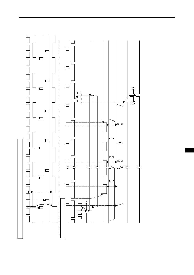
15-77
15
MSM66591/ML66592
User's
Manual
Chapter 15 Serial Port Functions
Figure 15-34 Example of Timing Diagram in Receive Synchronous Normal Master Mode
: BRG1 divided by 1/4
: receive shift clock
1/4 BRG1
SR1CLK
CLK : master clock
SR1REN : receive enable signal (bit 7of SR1CON)
RXD1 (pin) : receive data input from pin (P6_2)
LSR1BUF : receive end signal
RX1READY : receive interrupt request signal
Explanation of Symbols BRG1 :
clock pulse generated by baud rate generator (S1TM)
RXC1 (pin) : receive shift clock output from pin (P6_4)
INRXD : receive data sampled from RXD1 by the RXD sampling clock
signal that indicates beginning of an instruction
M1S1
Sampling CLK1 :
WSR1CON :
SR1FREE : signal that indicates receiving ("0")
write signal to SR1CON
clock to sample data received at RXD1
Timing for generation of sampling CLK1, SR1CLK, and RXC1 (pin) by 1/4 BRG
BRG1
1/4 BRG1
Sampling CLK1
SR1CLK
RXC1 (pin )
Sampling CLK1
Receive timing (with parity bit)
SR1CLK
CLK
WSR1CON
SR1REN
SR1FREE
RXC1 (pin)
RXD1 (pin)
INRXD
LSR1BUF
M1S1
RX1READY
RXC1 start
RXC1 stop
D (LSB)
D (LSB)
D (bit 1)
D (MSB)PARITY BIT
PARITY BIT
D (MSB)
D (bit 7)
:
4
3
2
1
4
3
2
1
4
3
2
1
4
3
2
1
4
3
2
1
4
3
2
1

15-78
MSM66591/ML66592 User's Manual
Chapter 15 Serial Port Functions
<Synchronous Normal Slave Mode (SCI1 only)>
The receive operation starts when SR1REN of SR1CON is set to "1" by the program.
SR1FREE, that indicates receiving, becomes "L" level, and the receive shift clock to
input to the RXC1 pin is accepted (refer to Figure 15-35).
The receive shift clock detects the edge synchronizing with the CLK to generate
SR1CLK.
Receive data is controlled synchronizing with SR1CLK.
If the RXC1 pin becomes "L" level, and then becomes "H" level, the receive shift clock
SR1CLK is generated by the edge detection circuit.
If SR1CLK is generated, the receive data just sampled the RXD1 pin is shifted in the
receive register.
The RXD1 pin is sampled while the RXC1 pin is in "L" level. The timing to shift in the
receive register occurs after the RXC1 pin rises. Therefore the transmit side transmits
data synchronizing with the fall of the RXC1 pin, which is the fall of the transmit shift
clock.
Hereafter, receive data is shifted in the receive register sequentially, synchronizing with
the receive shift clock, which is input according to the specification of SR1CON.
If the receive shift clock finally rises, SR1CLK acquired by edge detection is generated,
and the final receive data is input. Then 1 CLK later, the receive end signal LSR1BUF is
generated.
If LSR1BUF is generated, the content of the receive register (receive data) is trans-
ferred to S1BUF, an overrun error and parity error (if parity bit exists) are set, the
receive interrupt request signal (RX1READY) is generated, synchronizing with the
M1S1 signal that indicates the beginning of an instruction, and the interrupt request flag
(QSCI1) is set to "1". Then SR1FREE becomes "H" level. At this time SR1REN of
SR1CON does not become "L" level, and the receive operation starts again if the next
receive shift clock is input.
<Synchronous Multiprocessor Communication Slave Mode (SCI1 only)>
In synchronous multiprocessor communication slave mode, receive is controlled by the
same timing as synchronous normal slave mode. The differences are shown below.
∑ Setting of multiprocessor communication error
∑ If SR1MPC of SR1CON is "0", receive data is accepted regardless of the MPC bit of
receive data. When SR1MPC of SR1CON is "1", receive data is accepted if the MPC
bit of receive data is "1", but receive data is not accepted if the MPC bit of receive
data is "0". This means that data shifted in the shift register will not be loaded to
S1BUF, and also that an interrupt request will not be generated.

15-79
15
MSM66591/ML66592
User's
Manual
Chapter 15 Serial Port Functions
CLK
RXC1 (pin)
Edge detection
SR1CLK
Sampling CLK1
Explanation of Symbols CLK
RXC1 (pin)
Edge detection
SR1CLK
Sampling CLK1
: master clock
: receive shift clock input from pin (P6_4)
: receive shift clock in which RXC1 pin input edge is detected by CLK
: receive shift clock
: clock to sample receive data
RXC1"L"period
Timing for generation of sampling CLK1 and SR1CLK by RXC1(pin) edge detection

15-80
MSM66591/ML66592
User's
Manual
Chapter 15 Serial Port Functions
Receive timing (with parity bit)
SR1CLK
RXD1 (pin)
INRXD
LSR1BUF
M1S1
RX1READY
D (LSB)
D (bit 1)
D (LSB)
D (LSB)D (bit 6)
D (LSB)
D (MSB)
D (MSB)
D (bit 6)
Sampling CLK1
CLK
WSR1CON
SR1REN
SR1FREE
RXC1 (pin)
PARITY
BIT
PARITY
BIT
D (bit 1)
SR1CLK
WSR1CON
SR1FREE
RXD1 (pin)
LSR1BUF
RX1 READY
: receive shift clock
: write signal to SR1CON
: signal that indicates receiving ("0")
: receive data input from pin (P6_2)
: receive end signal
: receive interrupt request signal
Explanation of Symbols Sampling CLK1
CLK
SR1REN
RXC1 (pin)
INRXD
M1S1
: clock to sample receive data
: master clock
: receive enable signal (bit 7 of SR1CON)
: receive shift clock input from pin (P6_4)
: receive data sampled from RXD1 by the RXD sampling clock
: signal that indicates the beginning of an instruction
Figure 15-35 Example of Timing Diagram in Receive Synchronous Normal Slave Mode (2)

15-81
15
MSM66591/ML66592 User's Manual
Chapter 15 Serial Port Functions
[2]
4-Stage Buffer Mode
The 4-stage buffer mode is entered by setting SRnEXP (bit 3) of SRnCON. During the
4-stage buffer mode, consecutive reception of up to a maximum of 4 bytes is possible.
After 4 bytes are received, they can be collectively processed by an interrupt.
<4-Stage Buffer Mode with UART Reception: SCI0 Example>
During the 4-stage buffer mode, the receive buffers form a ring buffer configuration. At
the completion of each 1-byte reception, the contents of the receive register (receive
data) are transferred to a receive buffer in the order of S0BUF0, S0BUF1, S0BUF2,
S0BUF3, S0BUF0, etc. Therefore, data is received up to the S0BUFn receive buffer
(where n = 0 to 3). After processing that data, if reception is continued, data is received
beginning from the S0BUF(n + 1) buffer.
For example, after receiving data up to S0BUF1 and processing that data, the next data
reception begins with S0BUF2. Or, after receivingdata up to S0BUF3 and processing
that data, the next data reception begins with S0BUF0.
After receiving data up to S0BUFn and processing that data, if it is desired to receive m
consecutive bytes (m
4) of data and then process that data by an interrupt, since an
interrupt will be generated after data is received in the S0BUF(n + 1) through S0BUF(n
+ m) buffers, enable interrupt requests for S0BUF(n + m), the last buffer to receive data,
and then receive the data.
For example, after completing processing up to S0BUF2, if it is desired to receive 3
consecutive bytes of data and then process that data by an interrupt, since the 3 bytes
of data will be received in the order of S0BUF3, S0BUF0, and S0BUF1, enable interrupt
generation only for S0BUF1, the last buffer to receive data, and then begin the data
reception. To enable interrupt generation for S0BUF1, set RV0IE1 (SCI0 receive
interrupt enable flag) of SR0INT to "1". In this case, after reception is completed for
S0BUF3 through S0BUF1, an SCI0 receive complete interrupt request is generated,
and the SCI0 receive interrupt request flags (RV0IRQ1 of SR0INT and QSCI0 of
IRQ1L) are set.
Because a parity error flag, multiprocessor communication flag and overrun error flag
are provided for each receive buffer (4 bits in total), data reception errors can be
verified by reading the error flags that correspond to buffers. The framing error flag
consists of 1 bit. If a framing error occurs even in just 1 byte of the received data, the
framing error flag will be set to "1" at that time.
If 5 or more bytes of data are consecutively received, new data will overwrite the pre-
vious data, beginning with the receive buffer that received the first data. At that time, if
the data transferred to the receive buffer during the previous receive operation has not
been read by the CPU, the overrun error flag of each receive buffer will be set to "1".
After a framing or other error has occurred, read BFCU00 (bit 4) and BFCU01 (bit 5) of
S0STAT2 to verify which receive buffer will data be transferred to at the completion of
the next reception.
Receive timing in 1 frame of the 4-stage buffer mode is controlled in the same manner
as reception in the single buffer mode.
SCI2, SCI3 and SCI4 also operate in the same manner.
Figure 15-36 shows a timing example of the 4-stage buffer mode with UART reception.

15-82
MSM66591/ML66592
User's
Manual
Chapter 15 Serial Port Functions
Figure 15-36 Example of Timing Diagram in Receive UART 4-Stage Buffer Mode
RXDn (pin)
LSRnBUF
M1S1
RXnREADY
SnBUF0
SnBUF1
SnBUF2
SnBUF3
Explanation
of Symbols
Data 1
Data 2
Data 3
Data 4
Data 5
Data 1
Data 2
Data 3
Data 4
Data 5
1-frame
1-frame
1-frame
1-frame
1-frame
LSRnBUF: receive end signal
RXnREADY: receive interrupt request signal
RxDn (pin): receive data input from pin
M1S1: signal that indicates beginning of an instruction
SnBUF0: SCIn receive buffer 0
SnBUF1: SCIn receive buffer 1
SnBUF2: SCIn receive buffer 2
SnBUF3: SCIn receive buffer 3
n = 0, 2, 3, 4

A/D Converter Functions
Chapter 16
16


16-1
MSM66591/ML66592 User's Manual
Chapter 16 A/D Converter Functions
16
16. A/D Converter Functions
The MSM66591/ML66592 have two sets of 10-bit A/D converters that support 12
channels of analog input, A/D Converter 0 (ADC0) and A/D Converter 1 (ADC1).
The basic configuration of A/D converter 0 and A/D converter 1 is the same, with the
only difference being the address of registers located in the SFR area.
Each A/D converter has three modes of operation: a scan mode that sequentially
converts selected multiple channels, a select mode that converts one selected channel,
and a hard select mode that activates the select mode when an interrupt request is
generated.
A successive approximation method using the Sample & Hold function is utilized to
convert analog quantities to digital quantities. The converted result is stored in the A/D
result registers (ADCR0≠ADCR23).
Corresponding to ch0≠ch23, pins AI0≠AI23 are available as analog input-only pins.
Operation of the A/D converters is controlled by control registers located in the SFR
area (ADCON0L, ADCON0H, ADCON1L and ADCON1H).
Interrupts by the A/D converters in the scan, select or hard select modes are assigned
to the same interrupt vector. The generation of each interrupt factor (Yes/No) and
interrupt generation (Enable/Disable) are controlled by two 6-bit A/D interrupt control
registers (ADINTCON0 and ADINTCON1).
Figures 16-1 and 16-2 show the configurations of A/D Converter 0 and A/D Converter 1,
respectively. Table 16-1 lists the SFRs for A/D converter control.
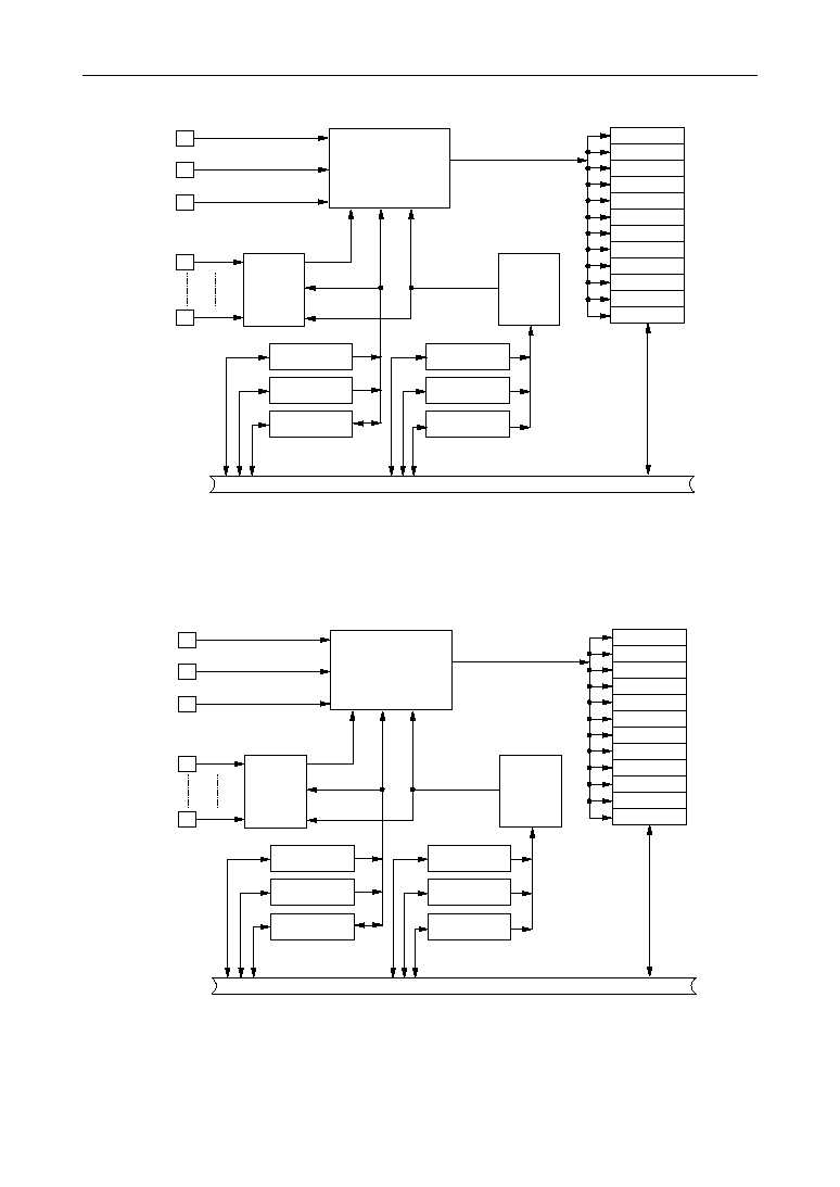
16-2
MSM66591/ML66592 User's Manual
Chapter 16 A/D Converter Functions
ADCR0
ADCR1
ADCR2
ADCR3
ADCR4
ADCR5
ADCR6
ADCR7
ADCR8
ADCR9
ADHENCON
Internal Bus
AV
DD
V
REF
AGND
AI0
AI11
ADCON0L
ADCR10
ADCR11
ADHSEL0
ADCON0H
ADINTCON0
ADHSCON
A/D
Conversion
Circuit
Interrupt
Request
Selector
Analog
Selector
Figure 16-1 Configuration of A/D Converter 0 (ADC0)
For A/D converter specifications, see Chapter 25, "Electrical Characteristics."
Figure 16-2 Configuration of A/D Converter 1 (ADC1)
ADCR12
ADCR13
ADCR14
ADCR15
ADCR16
ADCR17
ADCR18
ADCR19
ADCR20
ADCR21
ADHENCON
Internal Bus
AV
DD
V
REF
AGND
AI12
AI23
ADCON1L
ADCR22
ADCR23
ADHSEL1
ADCON1H
ADINTCON1
ADHSCON
A/D
Conversion
Circuit
Interrupt
Request
Selector
Analog
Selector
16-3
MSM66591/ML66592 User's Manual
Chapter 16 A/D Converter Functions
16
Table 16-1 A/D Converter Contol SFR List
00F1
00E1
00E2
00E3
00E4
00E5
00E6
00E7
00E8
00E9
00EA
00EB
00EC
00ED
00EE
00EF
00F0
00F2
00F3
00F4
00F5
00F6
00F7
00F8
00F9
00FA
00FB
00FC
00FD
00FE
00FF
0158
0159
015A
015B
FC
C0
ADHSCON
ADINTCON1
A/D Interrupt Control Register 1
R/W
16
*R/W
C0
00
ADINTCON0
ADHENCON
A/D Interrupt Control Register 0
ADHSEL0
00E0
0000
--
A/D Hard Select Register 0
0000
--
A/D Result Register 0
--
Undefined
ADCR0
--
--
A/D Hard Select Enable Register
16
--
R/W
8
A/D Hard Select Software Control Register
ADHSEL1
A/D Hard Select Register 1
A/D Result Register 1
--
Undefined
ADCR1
A/D Result Register 2
--
Undefined
ADCR2
A/D Result Register 3
--
Undefined
ADCR3
A/D Result Register 4
--
Undefined
ADCR4
A/D Result Register 5
--
Undefined
ADCR5
A/D Result Register 6
--
Undefined
ADCR6
A/D Result Register 7
--
Undefined
ADCR7
A/D Result Register 8
--
Undefined
ADCR8
A/D Result Register 9
--
Undefined
ADCR9
A/D Result Register 10
--
Undefined
ADCR10
A/D Result Register 11
--
Undefined
ADCR11
A/D0 Control Register L
ADCON0L
80
--
A/D0 Control Register H
ADCON0H
80
--
A/D Result Register 12
--
Undefined
ADCR12
A/D Result Register 13
--
Undefined
ADCR13
A/D Result Register 14
--
Undefined
ADCR14
A/D Result Register 15
--
Undefined
ADCR15
A/D Result Register 16
--
Undefined
ADCR16
A/D Result Register 17
--
Undefined
ADCR17
A/D Result Register 18
--
Undefined
ADCR18
A/D Result Register 19
--
Undefined
ADCR19
A/D Result Register 20
--
Undefined
ADCR20
A/D Result Register 21
--
Undefined
ADCR21
A/D Result Register 22
--
Undefined
ADCR22
A/D Result Register 23
--
Undefined
ADCR23
A/D1 Control Register L
ADCON1L
80
--
A/D1 Control Register H
ADCON1H
80
--
--
R/W
8
*R/W
16
Address [H]
Name
Abbreviated
Name (BYTE)
R/W
8/16-Bit
Operation
Reset
State [H]
Abbreviated
Name (WORD)
[Notes]
1.
Some addresses are not consecutive.
2.
Addresses in the address column marked by "" indicate that the register has bits missing.
3.
*R/W indicates a special operation. Data can be written to the even number A/D result registers
(ADCR0, 2, 4, 6, 8, 10 and ADCR12, 14, 16, 18, 20, 22) and odd number A/D result registers (ADCR1, 3,
5, 7, 9, 11 and ADCR13, 15, 17, 19, 21, 23) separately in the following way:
- When data is written to ADCR0, the data is also written to ADCR0≠ADCR10 at the same time; when
data is written to ADCR12, the data is also written to ADCR12≠ADCR22 at the same time.
- When data is written to ADCR1, the data is also written to ADCR1≠ADCR11; when data is written to
ADCR13 at the same time, the data is also written to ADCR13≠ADCR23 at the same time.

16-4
MSM66591/ML66592 User's Manual
Chapter 16 A/D Converter Functions
16.1 Configuration of A/D Converter
Since the basic configurations of the A/D converter 0 and the A/D converter 1 are the
same, this section chiefly explains the configuration of A/D converter 0.
The A/D converter has three operation modes: scan mode, select mode, and hard
select mode.
[1]
Scan Mode
In scan mode, A/D conversion is sequentially performed from any channel out of ch0≠
ch11 to ch11 (from any of ch12≠ch23 to ch23 for A/D converter 1). The scan mode is
mainly controlled by the A/D control register L (ADCON0L, ADCON1L). In scan mode,
the scan mode provides the selection whether to stop A/D conversion at the end of A/D
conversion for ch11 (ch23 for A/D converter 1) or to restart A/D conversion automati-
cally from the first channel specified.
[2]
Select Mode
In select mode, any channel of ch0≠ch11 (any of ch12≠ch23 for A/D converter 1) is
specified, and A/D conversion is performed for the specified channel. The select mode
is mainly controlled by the A/D control register H (ADCON0H, ADCON1H).
It is also possible to operate select mode during scan mode operation. In this case, A/D
conversion for a channel that A/D conversion is progressing for in scan mode, is
suspended at that point when select mode is specified, and A/D conversion for the
channel specified in select mode is performed. When A/D conversion in select mode
ends, A/D conversion in scan mode restarts from the suspended channel.
ch0
ch1
ch2
ch2
ch3
ch4
q
w
A/D conversion in scan mode
A/D conversion in select mode
q
A/D conversion for ch2 is suspended.
A/D conversion for ch4 in select mode starts.
A/D conversion for ch4 ends.
A/D conversion from ch2 in scan mode restarts.
w
Figure 16-3 Timing Diagram During Select Mode Operation in Scan Mode
[3]
Hard Select Mode
The hard select mode specifies a channel from ch0 to ch3 (from ch12 to ch15 for A/D
converter 1) and performs A/D conversion of the channel when an interrupt request is
generated.
16-5
MSM66591/ML66592 User's Manual
Chapter 16 A/D Converter Functions
16
The channels from ch0 to ch3 and ch12 to ch15 are prioritized as shown in Table 16-3.
Table 16-3 A/D Conversion Mode Priorities
Mode
Priority
Hard select mode ch0 (ch12)
Hard select mode ch1 (ch13)
Hard select mode ch2 (ch14)
Hard select mode ch3 (ch15)
Select Mode
Scan Mode
High
Low
Priority
1
PWC0/PWC1 underflow or match
2
PWC2/PWC3 underflow or match
3
PWC4/PWC5 underflow or match
4
PWC6/PWC7 underflow or match
5
PWC0/PWC1 match
6
PWC2/PWC3 match
7
PWC4/PWC5 match
8
PWC6/PWC7 match
9
CAP0 event generation
10
CAP1 event generation
11
GTMC/GEVC overflow
12
CAP15 event generation
13
FTM16 event generation
14
FTM17 event generation
15
Soft 0 (bit 0 of ADHSCON set by the program)
16
Soft 1 (bit 1 of ADHSCON set by the program)
Interrupt Cause
The A/D hard select mode is controlled by the A/D hard select register 0 (ADHSEL0), A/
D hard select register 1 (ADHSEL1), and A/D hard select enable register
(ADHENCON).
An interrupt source to activate the A/D hard select mode is set to each channel (ch0≠
ch3 and ch12≠ch15) of the ADHSEL0 and ADHSEL1. An effective channel (ch0≠ch3
and ch12≠ch15) under the A/D hard select mode is set to the ADHENCON.
The change of the interrupt cause of a current channel during hard select mode opera-
tion is invalid.
Table 16-2 lists the interrupt causes to activate the A/D hard select mode.
Table 16-2 Interrupt Causes To Activate A/D Hard Select Mode
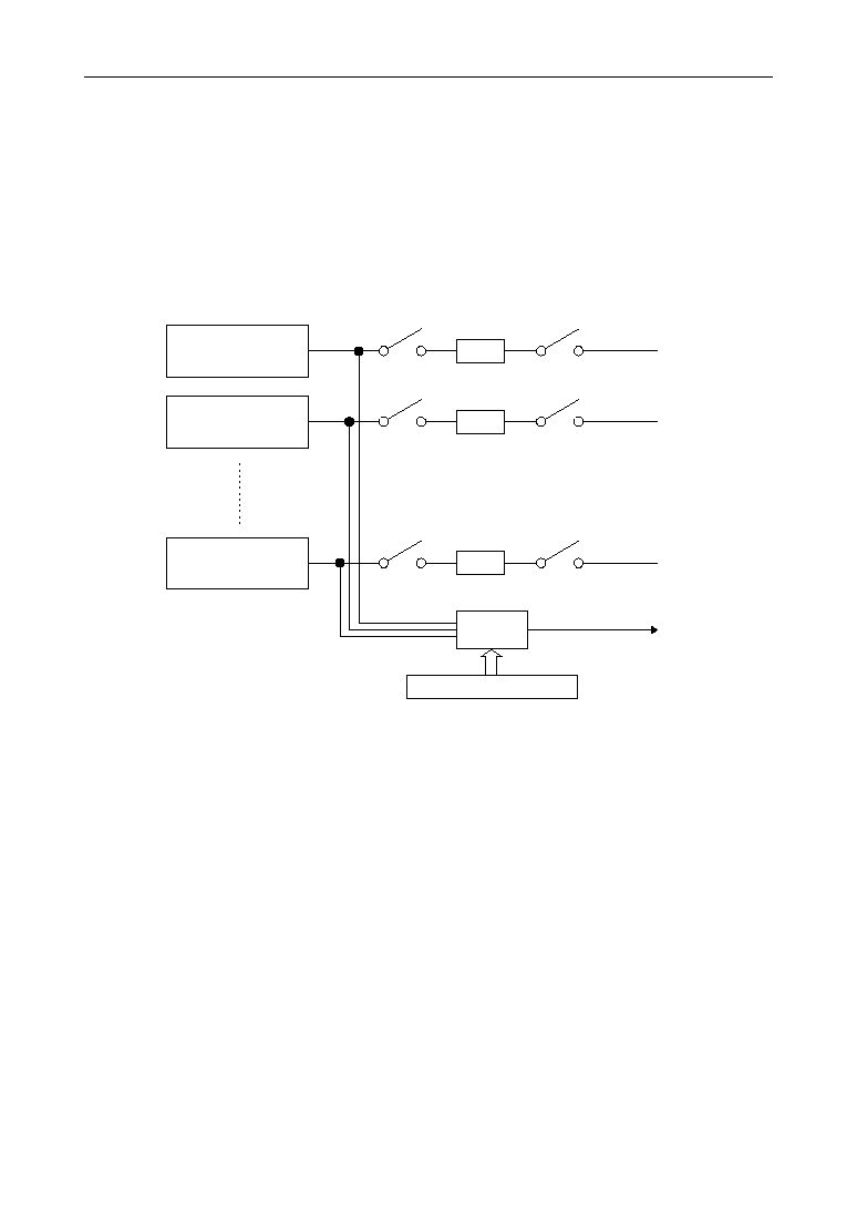
16-6
MSM66591/ML66592 User's Manual
Chapter 16 A/D Converter Functions
If a higher priority mode A/D conversion request is generated while a lower priority
mode A/D conversion is being performed, the ongoing A/D conversion is suspended
and restarts after completion of the requested convension.
If, during execution of A/D conversion, a request for A/D conversion in the same mode
(interrupt source) as the ongoing A/D conversion is generated, the ongoing A/D conver-
sion is given priority and the generated A/D conversion request is ignored.
Figure 16-4 shows the configuration of A/D hard select mode.
Figure 16-4 A/D Hard Select Mode Configuration
Dxxx
Exxx
Qxxx
*Interrupt cause
generation source
Dxxx
Exxx
Qxxx
*Interrupt cause
generation source
Dxxx
Exxx
Qxxx
*Interrupt cause
generation source
Selector
* Only the interrupt
causes listed in Table 16-2
can activate the A/D hard
select mode.
A/D hard select register
A/D hard select request
(IRQD)
(IRQ)
(IE)

16-7
MSM66591/ML66592 User's Manual
Chapter 16 A/D Converter Functions
16
16.2 Control Register of A/D Converter
[1]
A/D Control Register 0L (ADCON0L)
ADCON0L is a 7-bit register that primarily controls the scan mode of the A/D converter.
Figure 16-5 shows the configuration of ADCON0L.
At reset (when the
RES
signal is input, the BRK instruction is executed, the watchdog
timer is overflown, or an operation code trap is generated), ADCON0L becomes 80H.
<Description of Each Bit>
∑ ADSNM00≠ADSNM03 (bit 0≠bit 3)
These 4 bits specify the scan channel in scan mode.
Change the scan channel after setting ADRUN0 (bit 4) to "0". When ADRUN0 is "1"
(when A/D conversion is running in scan mode), changing the scan channel is invalid.
∑ ADRUN0 (bit 4)
This bit specifies RUN/STOP of A/D conversion in scan mode.
If this bit is "1", A/D conversion RUN is selected, and if "0", A/D conversion STOP is
selected. When A/D conversion STOP is selected by setting SCNC0 (bit 6) to "1" after
a scan cycle is completed, ADRUN0 does not automatically become "0", even if A/D
conversion stops after a scan cycle is completed.
∑ SNEX0 (bit 5)
This bit specifies the A/D conversion start factor in scan mode.
If this bit is "0", the next conversion starts when the A/D conversion is over. If this bit
is "1", 1 channel A/D conversion starts at each valid edge of the external interrupt
input pin (INT1). At this time, bit 1 of the Port 6 secondary function control register
must be set to to "1", and the INT1 pin must be set to the secondary function.
Operation examples 1, 2 and 3 when SNEX0 is set to "1" are shown below.
1. In the case of an initial start, ADRUN0 is set to "1", and at the same time the first
channel of the scan channel is A/D converted. Then the 2nd or later channels of the
scan channels are sequentially A/D converted, synchronizing with the valid edge of
INT1.
2. When A/D conversion is stopped after the completion of a scan channel cycle, if A/
D conversion is restarted by setting INTSN0 to "0" by the program, A/D conversion
starts from the first channel of the scan channels, synchronizing with the valid edge of
INT1.
3. In other cases, set ADRUN0 and SNEX0 to "0" simultaneously by the program, and
set ADRUN0 and SNEX0 simultaneously to "1" by the program again. In this case the
first channel of the scan channels is A/D converted as soon as ADRUN0 becomes
"1". After that, A/D conversion is performed in synchronization with the valid edge of
INT1.
16-8
MSM66591/ML66592 User's Manual
Chapter 16 A/D Converter Functions
Figure 16-5 Configuration of ADCON0L
--
SCNC0
SNEX0 ADRUN0
ADSNM03 ADSNM02 ADSNM01 ADSNM00
7
6
5
4
3
2
1
0
"--" indicates a bit that is not provided.
"1" is read if a read instruction is executed.
ADSNM0
A/D Converter 0 Scan Channel
3 2 1 0
0 0 0 0 ch0≠ch11
0 0 0 1 ch1≠ch11
0 0 1 0 ch2≠ch11
0 0 1 1 ch3≠ch11
0 1 0 0 ch4≠ch11
0 1 0 1 ch5≠ch11
0 1 1 0 ch6≠ch11
0 1 1 1 ch7≠ch11
1 0 0 0 ch8≠ch11
1
1 ch9≠ch11
0 Scan mode A/D conversion STOP
1 Scan mode A/D conversion RUN
0
Next conversion starts when conversion ends
1
Next conversion starts at valid edge of INT1
0
Next conversion starts when cycle is completed
1
Conversion stops when cycle is completed
0 0
1 0 1 0 ch10, ch11
1 0 1 1 ch11
1 1
*
* Setting inhibited
ADCON0L
∑ SCNC0 (bit 6)
This bit specifies the operation after a scan channel cycle is completed.
If this bit is "0", A/D conversion starts from the first channel again, after a scan
channel cycle is completed. If this bit is "1", A/D conversion stops after the scan
channel cycle is completed. ADRUN0 (bit 4), however, does not become "0".
Use the following procedure (1) or (2) to perform the A/D conversion again.
(1) Set INTSN0 of ADINCON0 bit 0 to "0" by the program.
(2) Set SCNC0 to "0" by the program.
In this procedure the next conversion start mode is entered.
(Note that setting ADRUN0 to "1" again by the program does not start A/D conver-
sion again.)

16-9
MSM66591/ML66592 User's Manual
Chapter 16 A/D Converter Functions
16
[2]
A/D Control Register 1L (ADCON1L)
ADCON1L is a 7-bit register that primarily controls the scan mode of the A/D converter.
Figure 16-6 shows the configuration of ADCON1L.
At reset (when the
RES
signal is input, the BRK instruction is executed, the watchdog
timer is overflown, or an operation code trap is generated), ADCON1L becomes 80H.
<Description of Each Bit>
∑ ADSNM10≠ADSNM13 (bit 0≠bit 3)
These 4 bits specify the scan channel in scan mode.
Change the scan channel after setting ADRUN1 (bit 4) to "0". When ADRUN1 is "1"
(when A/D conversion is running in scan mode), changing the scan channel is invalid.
∑ ADRUN1 (bit 4)
This bit specifies RUN/STOP of A/D conversion in scan mode.
If this bit is "1", A/D conversion RUN is selected, and if "0", A/D conversion STOP is
selected. When A/D conversion STOP is selected by setting SCNC1 (bit 6) to "1" after
a scan cycle is completed, ADRUN1 does not automatically become "0", even if A/D
conversion stops after a scan cycle is completed.
∑ SNEX1 (bit 5)
This bit specifies the A/D conversion start factor in scan mode.
If this bit is "0", the next conversion starts when the A/D conversion is over. If this bit
is "1", 1 channel A/D conversion starts at each valid edge of the external interrupt
input pin (INT1). At this time, bit 1 of the Port 6 secondary function control register
must be set to to "1", and the INT1 pin must be set to the secondary function.
Operation examples 1, 2 and 3 when SNEX1 is set to "1" are shown below.
1. In the case of an initial start, ADRUN1 is set to "1", and at the same time the first
channel of the scan channel is A/D converted. Then the 2nd or later channels of the
scan channels are sequentially A/D converted, synchronizing with the valid edge of
INT1.
2. When A/D conversion is stopped after the completion of a scan channel cycle, if A/
D conversion is restarted by setting INTSN1 to "0" by the program, A/D conversion
starts from the first channel of the scan channels, synchronizing with the valid edge of
INT1.
3. In other cases, set ADRUN1 and SNEX1 to "0" simultaneously by the program, and
set ADRUN1 and SNEX1 simultaneously to "1" by the program again. In this case the
first channel of the scan channels is A/D converted as soon as ADRUN1 becomes
"1". After that, A/D conversion is performed in synchronization with the valid edge of
INT1.

16-10
MSM66591/ML66592 User's Manual
Chapter 16 A/D Converter Functions
∑ SCNC1 (bit 6)
This bit specifies the operation after a scan channel cycle is completed.
If this bit is "0", A/D conversion starts from the first channel again, after a scan
channel cycle is completed. If this bit is "1", A/D conversion stops after the scan
channel cycle is completed. ADRUN1 (bit 4), however, does not become "0".
Use the following procedure (1) or (2) to perform the A/D conversion again.
(1) Set INTSN1 of ADINCON1 bit 0 to "0" by the program.
(2) Set SCNC1 to "0" by the program.
In this procedure the next conversion start mode is entered.
(Note that setting ADRUN1 to "1" again by the program does not start A/D conver-
sion again.)
Figure 16-6 Configuration of ADCON1L
--
SCNC1
SNEX1 ADRUN1
ADSNM13 ADSNM12 ADSNM11 ADSNM10
7
6
5
4
3
2
1
0
"--" indicates a bit that is not provided.
"1" is read if a read instruction is executed.
ADSNM1
A/D Converter 1 Scan Channel
3 2 1 0
0 0 0 0 ch12≠ch23
0 0 0 1 ch13≠ch23
0 0 1 0 ch14≠ch23
0 0 1 1 ch15≠ch23
0 1 0 0 ch16≠ch23
0 1 0 1 ch17≠ch23
0 1 1 0 ch18≠ch23
0 1 1 1 ch19≠ch23
1 0 0 0 ch20≠ch23
1
1 ch21≠ch23
0 Scan mode A/D conversion STOP
1 Scan mode A/D conversion RUN
0
Next conversion starts when conversion ends
1
Next conversion starts at valid edge of INT1
0
Next conversion starts when cycle is completed
1
Conversion stops when cycle is completed
0 0
1 0 1 0 ch22, ch23
1 0 1 1 ch23
1 1
*
* Setting inhibited
ADCON1L

16-11
MSM66591/ML66592 User's Manual
Chapter 16 A/D Converter Functions
16
[3]
A/D Control Register 0H (ADCON0H)
The ADCON0H is a 7-bit register that primarily controls the select mode of the A/D
converter 0.
Figure 16-7 shows the configuration of ADCON0H.
At reset (when the
RES
signal is input, the BRK instruction is executed, the watchdog
timer is overflown, or an operation code trap is generated), ADCON0H becomes 80H.
<Description of Each Bit>
∑ ADSTM00≠ADSTM03 (bit 0≠bit 3)
These 4 bits specify the A/D conversion channel in select mode.
Change the select channel after setting STS0 (bit 4) to "0". When STS0 is "1" (when
A/D conversion is running in select mode), changing the select channel is invalid.
∑ STS0 (bit 4)
This bit specifies RUN/STOP of A/D conversion in select mode.
If this bit is "1", A/D conversion of the channel specified by ADSTM00≠ADSTM03 (bit
0≠bit 3) starts. This bit becomes "0" when A/D conversion ends.
∑ ADTM00, ADTM01 (bit 5, bit 6)
These 2 bits specify the number of clocks required for A/D conversion per channel.
Basically, the more the number of clocks required for A/D conversion is increased
(i.e. the longer the time required for A/D conversion is made), the higher the accu-
racy will be.
Changing the number of clocks during A/D conversion is ignored.
16-12
MSM66591/ML66592 User's Manual
Chapter 16 A/D Converter Functions
Figure 16-7 Configuration of ADCON0H
--
ADTM01 ADTM00
STS0
ADSTM03 ADSTM02 ADSTM01 ADSTM00
7
6
5
4
3
2
1
0
"*" indicates either "0" or "1".
"--" indicates a bit that is not provided.
"1" is read if a read instruction is executed.
ADSTM0
A/D Converter 0 Select Channel
3 2 1 0
0 0 0 0
ch0
0 0 0 1
ch1
0 0 1 0
ch2
0 0 1 1
ch3
0 1 0 0
ch4
0 1 0 1
ch5
0 1 1 0
ch6
0 1 1 1
ch7
1 0 0 0
ch8
1
1
ch9
0
Select mode A/D conversion STOP
1
Select mode A/D conversion RUN
ADTM0
1
0
0
0
512 CLK (21.3 ms)
0
1
384 CLK
1
*
256 CLK
1 0 1 0
ch10
1 0 1 1
ch11
1 1
*
*
Setting inhibited
0 0
Number of clocks for A/D
conversion per channel
(f = 24 MHz)
ADCON0H

16-13
MSM66591/ML66592 User's Manual
Chapter 16 A/D Converter Functions
16
[4]
A/D Control Register 1H (ADCON1H)
The ADCON1H is a 7-bit register that primarily controls the select mode of the A/D
converter 1.
Figure 16-8 shows the configuration of ADCON1H.
At reset (when the
RES
signal is input, the BRK instruction is executed, the watchdog
timer is overflown, or an operation code trap is generated), ADCON1H becomes 80H.
<Description of Each Bit>
∑ ADSTM10≠ADSTM13 (bit 0≠bit 3)
These 4 bits specify the A/D conversion channel in select mode.
Change the select channel after setting STS1 (bit 4) to "0". When STS1 is "1" (when
A/D conversion is running in select mode), changing the select channel is invalid.
∑ STS1 (bit 4)
This bit specifies RUN/STOP of A/D conversion in select mode.
If this bit is "1", A/D conversion of the channel specified by ADSTM10≠ADSTM13 (bit
0≠bit 3) starts. This bit becomes "0" when A/D conversion ends.
∑ ADTM10, ADTM11 (bit 5, bit 6)
These 2 bits specify the number of clocks required for A/D conversion per channel.
Basically, the more the number of clocks required for A/D conversion is increased
(i.e. the longer the time required for A/D conversion is made), the higher the accu-
racy will be.
Changing the number of clocks during A/D conversion is ignored.

16-14
MSM66591/ML66592 User's Manual
Chapter 16 A/D Converter Functions
Figure 16-8 Configuration of ADCON1H
--
ADTM11 ADTM10
STS1
ADSTM13 ADSTM12 ADSTM11 ADSTM10
7
6
5
4
3
2
1
0
"*" indicates either "0" or "1".
"--" indicates a bit that is not provided.
"1" is read if a read instruction is executed.
ADSTM1
A/D Converter 1 Select Channel
3 2 1 0
0 0 0 0
ch12
0 0 0 1
ch13
0 0 1 0
ch14
0 0 1 1
ch15
0 1 0 0
ch16
0 1 0 1
ch17
0 1 1 0
ch18
0 1 1 1
ch19
1 0 0 0
ch20
1
1
ch21
0
Select mode A/D conversion STOP
1
Select mode A/D conversion RUN
ADTM1
1
0
0
0
512 CLK (21.3 ms)
0
1
384 CLK
1
*
256 CLK
1 0 1 0
ch22
1 0 1 1
ch23
1 1
*
*
Setting inhibited
0 0
Number of clocks for A/D
conversion per channel
(f = 24 MHz)
ADCON1H

16-15
MSM66591/ML66592 User's Manual
Chapter 16 A/D Converter Functions
16
[5]
A/D Interrupt Control Register 0 (ADINTCON0)
ADINTCON0 is a 6-bit register that primarily controls the interrupt request generation of
the A/D converter 0.
Figure 16-9 shows the configuration of ADINTCON0.
At reset (when the
RES
signal is input, the BRK instruction is executed, the watchdog
timer is overflown, or an operation code trap is generated), ADINTCON0 becomes
C0H.
<Description of Each Bit>
∑ INTSN0 (bit 0)
This bit indicates the completion of a scan channel cycle.
If this bit is "0", a cycle is not completed, and if "1", a cycle is completed. The phrase
"cycle is completed" indicates that the A/D conversion of ch11 is completed. This bit
must be reset to "0" by the program.
∑ INTST0 (bit 1)
This bit indicates the end of A/D conversion in select mode.
If this bit is "1", A/D conversion has ended. This bit must be reset to "0" by the
program.
∑ ADSNIE0 (bit 2)
This bit specifies enable/disable of an interrupt request generation when a scan
channel cycle is completed.
If this bit is "0", the interrupt request generation is disabled, and if "1", is enabled.
The phrase "cycle is completed" indicates that the A/D conversion of ch11 is com-
pleted.
∑ ADSTIE0 (bit 3)
This bit specifies enable/disable of an interrupt request generation to end A/D
conversion in select mode.
If this bit is "0", the interrupt request generation is disabled, and if "1", is enabled.
∑ INTHS0 (bit 4)
This bit indicates the end of A/D conversion in hard select mode.
"1" on this bit indicates end of A/D conversion in hard select mode.
This bit must be reset to "0" by the program.
∑ ADHSIE0 (bit 5)
This bit specifies enable/disable of an interrupt request generation to end A/D
conversion in hard select mode.
If this bit is "0", the interupt request generation is disabled, and if "1", is enabled.
16-16
MSM66591/ML66592 User's Manual
Chapter 16 A/D Converter Functions
Figure 16-9 Configuration of ADINTCON0
--
--
ADHSIE0
INTHS0 ADSTIE0ADSNIE0 INTST0 INTSN0
7
6
5
4
3
2
1
0
0 Scan channel cycle: no
1 Scan channel cycle: yes
0 Select mode end: no
1 Select mode end: yes
0
Interrupt request generation by INTSN0: disabled
1
Interrupt request generation by INTSN0: enabled
0
Interrupt request generation by INTST0: disabled
1
Interrupt request generation by INTST0: enabled
"--" indicates a bit that is not provided.
"1" is read if a read instruction is executed.
0
Hard Select mode end: no
1
Hard Select mode end: yes
0
Interrupt request generation by INTHS0: disabled
1
Interrupt request generation by INTHS0: enabled
ADINTCON0

16-17
MSM66591/ML66592 User's Manual
Chapter 16 A/D Converter Functions
16
[6]
A/D Interrupt Control Register 1 (ADINTCON1)
ADINTCON1 is a 6-bit register that primarily controls the interrupt request generation of
the A/D converter 1.
Figure 16-10 shows the configuration of ADINTCON1.
At reset (when the
RES
signal is input, the BRK instruction is executed, the watchdog
timer is overflown, or an operation code trap is generated), ADINTCON1 becomes
C0H.
<Description of Each Bit>
∑ INTSN1 (bit 0)
This bit indicates the completion of a scan channel cycle.
If this bit is "0", a cycle is not completed, and if "1", a cycle is completed. The phrase
"cycle is completed" indicates that the A/D conversion of ch23 is completed. This bit
must be reset to "0" by the program.
∑ INTST1 (bit 1)
This bit indicates the end of A/D conversion in select mode.
If this bit is "1", A/D conversion has ended. This bit must be reset to "0" by the
program.
∑ ADSNIE1 (bit 2)
This bit specifies enable/disable of an interrupt request generation when a scan
channel cycle is completed.
If this bit is "0", the interrupt request generation is disabled, and if "1", is enabled.
The phrase "cycle is completed" indicates that the A/D conversion of ch23 is com-
pleted.
∑ ADSTIE1 (bit 3)
This bit specifies enable/disable of an interrupt request generation to end A/D
conversion in select mode.
If this bit is "0", the interrupt request generation is disabled, and if "1", is enabled.
∑ INTHS1 (bit 4)
This bit indicates the end of A/D conversion in hard select mode.
"1" on this bit indicates end of A/D conversion in hard select mode.
This bit must be reset to "0" by the program.
∑ ADHSIE1 (bit 5)
This bit specifies enable/disable of an interrupt request generation to end A/D
conversion in hard select mode.
If this bit is "0", the interupt request generation is disabled, and if "1", is enabled.

16-18
MSM66591/ML66592 User's Manual
Chapter 16 A/D Converter Functions
Figure 16-10 Configuration of ADINTCON1
--
--
ADHSIE1
INTHS1 ADSTIE1ADSNIE1 INTST1 INTSN1
7
6
5
4
3
2
1
0
0 Scan channel cycle: no
1 Scan channel cycle: yes
0 Select mode end: no
1 Select mode end: yes
0
Interrupt request generation by INTSN1: disabled
1
Interrupt request generation by INTSN1: enabled
0
Interrupt request generation by INTST1: disabled
1
Interrupt request generation by INTST1: enabled
"--" indicates a bit that is not provided.
"1" is read if a read instruction is executed.
0
Hard Select mode end: no
1
Hard Select mode end: yes
0
Interrupt request generation by INTHS1: disabled
1
Interrupt request generation by INTHS1: enabled
ADINTCON1

16-19
MSM66591/ML66592 User's Manual
Chapter 16 A/D Converter Functions
16
[7]
A/D Hard Select Register 0 (ADHSEL0)
The ADHSEL0 register is used to set an interrupt cause to activate the hard select
mode of A/D converter 0 to individual channels. Channel 0, channel 1, channel 2, and
channel 3 each have 4 bits (total of 16 bits).
Figures 16-11 and 16-12 show the configurations of ADHSEL0.
Since only 16-bit data is accessible to ADHSEL0, bit manipulation instructions such as
SB and RB cannot be executed.
At reset (when the
RES
signal is input, the BRK instruction is executed, the watchdog
timer is overflown, or an operation code trap is generated), ADHSEL0 becomes 0000H.
<Description of Each Bit>
∑ ADHSEL0 bit 0≠bit 3
These four bits are used to set an A/D hard select mode activation interrupt cause to
channel 0.
∑ ADHSEL0 bit 4≠bit 7
These four bits are used to set an A/D hard select mode activation interrupt cause to
channel 1.
∑ ADHSEL0 bit 8≠bit 11
These four bits are used to set an A/D hard select mode activation interrupt cause to
channel 2.
∑ ADHSEL0 bit 12≠bit 15
These four bits are used to set an A/D hard select mode activation interrupt cause to
channel 3.
16-20
MSM66591/ML66592 User's Manual
Chapter 16 A/D Converter Functions
Figure 16-11 Configuration of ADHSEL0 (low-order bits)
7
6
5
4
3
2
1
0
3
2
1
A/D Hard Select Mode Activation
Interrupt Cause to Channel 0
0
0
0
0
0
0
0
0
1
0
0
1
0
1
0
0
1
0
0
1
1
0
1
1
PWC0/PWC1 underflow or match
PWC2/PWC3 underflow or match
PWC4/PWC5 underflow or match
PWC6/PWC7 underflow or match
PWC0/PWC1 match
PWC2/PWC3 match
PWC4/PWC5 match
PWC6/PWC7 match
0
0
1
0
1
0
1
0
1
1
0
0
1
0
0
1
0
1
1
0
1
1
1
0
1
1
0
1
1
1
1
1
1
CAP0 event generation
CAP1 event generation
GTMC/GEVC overflow
CAP15 event generation
FTM16 event generation
FTM17 event generation
Software 0 (ADHSCON bit 0 set)
Software 1 (ADHSCON bit 1 set)
0
1
0
1
0
1
0
1
7
6
5
A/D Hard Select Mode Activation
Interrupt Cause to Channel 1
0
0
0
0
0
0
0
0
1
0
0
1
0
1
0
0
1
0
0
1
1
0
1
1
PWC0/PWC1 underflow or match
PWC2/PWC3 underflow or match
PWC4/PWC5 underflow or match
PWC6/PWC7 underflow or match
PWC0/PWC1 match
PWC2/PWC3 match
PWC4/PWC5 match
PWC6/PWC7 match
4
0
1
0
1
0
1
0
1
1
0
0
1
0
0
1
0
1
1
0
1
1
1
0
1
1
0
1
1
1
1
1
1
CAP0 event generation
CAP1 event generation
GTMC/GEVC overflow
CAP15 event generation
FTM16 event generation
FTM17 event generation
Software 0 (ADHSCON bit 0 set)
Software 1 (ADHSCON bit 1 set)
0
1
0
1
0
1
0
1
ADHSEL0

16-21
MSM66591/ML66592 User's Manual
Chapter 16 A/D Converter Functions
16
Figure 16-12 Configuration of ADHSEL0 (high-order bits)
15
14
13
12
11
10
9
8
11 10 9
A/D Hard Select Mode Activation
Interrupt Cause to Channel 2
0
0
0
0
0
0
0
0
1
0
0
1
0
1
0
0
1
0
0
1
1
0
1
1
PWC0/PWC1 underflow or match
PWC2/PWC3 underflow or match
PWC4/PWC5 underflow or match
PWC6/PWC7 underflow or match
PWC0/PWC1 match
PWC2/PWC3 match
PWC4/PWC5 match
PWC6/PWC7 match
8
0
1
0
1
0
1
0
1
1
0
0
1
0
0
1
0
1
1
0
1
1
1
0
1
1
0
1
1
1
1
1
1
CAP0 event generation
CAP1 event generation
GTMC/GEVC overflow
CAP15 event generation
FTM16 event generation
FTM17 event generation
Software 0 (ADHSCON bit 0 set)
Software 1 (ADHSCON bit 1 set)
0
1
0
1
0
1
0
1
15 14 13
A/D Hard Select Mode Activation
Interrupt Cause to Channel 3
0
0
0
0
0
0
0
0
1
0
0
1
0
1
0
0
1
0
0
1
1
0
1
1
PWC0/PWC1 underflow or match
PWC2/PWC3 underflow or match
PWC4/PWC5 underflow or match
PWC6/PWC7 underflow or match
PWC0/PWC1 match
PWC2/PWC3 match
PWC4/PWC5 match
PWC6/PWC7 match
12
0
1
0
1
0
1
0
1
1
0
0
1
0
0
1
0
1
1
0
1
1
1
0
1
1
0
1
1
1
1
1
1
CAP0 event generation
CAP1 event generation
GTMC/GEVC overflow
CAP15 event generation
FTM16 event generation
FTM17 event generation
Software 0 (ADHSCON bit 0 set)
Software 1 (ADHSCON bit 1 set)
0
1
0
1
0
1
0
1
ADHSEL0 (bits 8≠15)

16-22
MSM66591/ML66592 User's Manual
Chapter 16 A/D Converter Functions
[8]
A/D Hard Select Register 1 (ADHSEL1)
The ADHSEL1 register is used to set an interrupt cause to activate the hard select
mode of A/D converter 1 to individual channels. Channel 12, channel 13, channel 14,
and channel 15 each have 4 bits (total of 16 bits).
Figures 16-13 and 16-14 show the configurations of ADHSEL1.
Since only 16-bit data is accessible to ADHSEL1, bit manipulation instructions such as
SB and RB cannot be executed.
At reset (when the
RES
signal is input, the BRK instruction is executed, the watchdog
timer is overflown, or an operation code trap is generated), ADHSEL1 becomes 0000H.
<Description of Each Bit>
∑ ADHSEL1 bit 0≠bit 3
These four bits are used to set an A/D hard select mode activation interrupt cause to
channel 12.
∑ ADHSEL1 bit 4≠bit 7
These four bits are used to set an A/D hard select mode activation interrupt cause to
channel 13.
∑ ADHSEL1 bit 8≠bit 11
These four bits are used to set an A/D hard select mode activation interrupt cause to
channel 14.
∑ ADHSEL1 bit 12≠bit 15
These four bits are used to set an A/D hard select mode activation interrupt cause to
channel 15.
16-23
MSM66591/ML66592 User's Manual
Chapter 16 A/D Converter Functions
16
Figure 16-13 Configuration of ADHSEL 1 (low-order bits)
7
6
5
4
3
2
1
0
3
2
1
A/D Hard Select Mode Activation
Interrupt Cause to Channel 12
0
0
0
0
0
0
0
0
1
0
0
1
0
1
0
0
1
0
0
1
1
0
1
1
PWC0/PWC1 underflow or match
PWC2/PWC3 underflow or match
PWC4/PWC5 underflow or match
PWC6/PWC7 underflow or match
PWC0/PWC1 match
PWC2/PWC3 match
PWC4/PWC5 match
PWC6/PWC7 match
0
0
1
0
1
0
1
0
1
1
0
0
1
0
0
1
0
1
1
0
1
1
1
0
1
1
0
1
1
1
1
1
1
CAP0 event generation
CAP1 event generation
GTMC/GEVC overflow
CAP15 event generation
FTM16 event generation
FTM17 event generation
Software 0 (ADHSCON bit 0 set)
Software 1 (ADHSCON bit 1 set)
0
1
0
1
0
1
0
1
7
6
5
A/D Hard Select Mode Activation
Interrupt Cause to Channel 13
0
0
0
0
0
0
0
0
1
0
0
1
0
1
0
0
1
0
0
1
1
0
1
1
PWC0/PWC1 underflow or match
PWC2/PWC3 underflow or match
PWC4/PWC5 underflow or match
PWC6/PWC7 underflow or match
PWC0/PWC1 match
PWC2/PWC3 match
PWC4/PWC5 match
PWC6/PWC7 match
4
0
1
0
1
0
1
0
1
1
0
0
1
0
0
1
0
1
1
0
1
1
1
0
1
1
0
1
1
1
1
1
1
CAP0 event generation
CAP1 event generation
GTMC/GEVC overflow
CAP15 event generation
FTM16 event generation
FTM17 event generation
Software 0 (ADHSCON bit 0 set)
Software 1 (ADHSCON bit 1 set)
0
1
0
1
0
1
0
1
ADHSEL1 (bits 0≠7)
16-24
MSM66591/ML66592 User's Manual
Chapter 16 A/D Converter Functions
Figure 16-14 Configuration of ADHSEL1 (high-order bits)
15
14
13
12
11
10
9
8
11 10 9
A/D Hard Select Mode Activation
Interrupt Cause to Channel 14
0
0
0
0
0
0
0
0
1
0
0
1
0
1
0
0
1
0
0
1
1
0
1
1
PWC0/PWC1 underflow or match
PWC2/PWC3 underflow or match
PWC4/PWC5 underflow or match
PWC6/PWC7 underflow or match
PWC0/PWC1 match
PWC2/PWC3 match
PWC4/PWC5 match
PWC6/PWC7 match
8
0
1
0
1
0
1
0
1
1
0
0
1
0
0
1
0
1
1
0
1
1
1
0
1
1
0
1
1
1
1
1
1
CAP0 event generation
CAP1 event generation
GTMC/GEVC overflow
CAP15 event generation
FTM16 event generation
FTM17 event generation
Software 0 (ADHSCON bit 0 set)
Software 1 (ADHSCON bit 1 set)
0
1
0
1
0
1
0
1
15 14 13
A/D Hard Select Mode Activation
Interrupt Cause to Channel 15
0
0
0
0
0
0
0
0
1
0
0
1
0
1
0
0
1
0
0
1
1
0
1
1
PWC0/PWC1 underflow or match
PWC2/PWC3 underflow or match
PWC4/PWC5 underflow or match
PWC6/PWC7 underflow or match
PWC0/PWC1 match
PWC2/PWC3 match
PWC4/PWC5 match
PWC6/PWC7 match
12
0
1
0
1
0
1
0
1
1
0
0
1
0
0
1
0
1
1
0
1
1
1
0
1
1
0
1
1
1
1
1
1
CAP0 event generation
CAP1 event generation
GTMC/GEVC overflow
CAP15 event generation
FTM16 event generation
FTM17 event generation
Software 0 (ADHSCON bit 0 set)
Software 1 (ADHSCON bit 1 set)
0
1
0
1
0
1
0
1
ADHSEL1 (bits 8≠15)
16-25
MSM66591/ML66592 User's Manual
Chapter 16 A/D Converter Functions
16
[9]
A/D Hard Select Software-Control Register (ADHSCON)
ADHSCON is a 2-bit register that activates, through software, A/D conversion in the A/
D hard select mode.
Writing a "1" to bit 1 or bit 0 of ADHSCON starts A/D conversion in the A/D hard select
mode.
Since these bits are not automatically cleared, they must be cleared by the software. A/
D conversion activated by these bits will begin after the rising edge of these bits is
detected. Therefore, once started, if conversion is to be restarted, first clear these bits
and then write a value of "1".
If a "1" is written to these bits during A/D conversion in the A/D hard select mode, the
next A/D conversion is reserved and will start after the present A/D conversion is
completed.
If "1" is written to bit 1 and bit 0 simultaneously, A/D conversion in the hard select mode
due to bit 1 (software 1) and A/D conversion in the hard select mode due to bit 0
(software 0) will be performed consecutively.
At reset (when the
RES
signal is input, the BRK instruction is executed, the watchdog
timer is overflown, or an operation code trap is generated), ADHSCON becomes FCH.
Figure 16-15 shows the configuration of ADHSCON.
Figure 16-15 Configuration of ADHSCON
7
--
6
--
5
--
4
--
3
--
2
1
0
0
1
Hard select mode A/D conversion activation: no
Hard select mode A/D conversion activation: yes
"--" indicates a bit that is not provided.
"1" is read if a read instruction is executed.
--
ADSOFT1 ADSOFT0
0
1
Hard select mode A/D conversion activation: no
Hard select mode A/D conversion activation: yes
ADHSCON

16-26
MSM66591/ML66592 User's Manual
Chapter 16 A/D Converter Functions
[10] A/D Hard Select Enable Register (ADHENCON)
ADHENCON is an 8-bit register that controls enable/disable of the hard select mode for
each channel (ch0, ch1, ch2, ch3, ch12, ch13, ch14, ch15).
Figure 16-16 shows the configuration of ADHENCON.
At reset (when the
RES
signal is input, the BRK instruction is executed, the watchdog
timer is overflown, or an operation code trap is generated), ADHENCON becomes 00H.
<Description of Each Bit>
∑ ADHENC0 (bit 0)
This bit enables or disables hard select A/D conversion on channel 0.
If this bit is "1", the hard select of channel 0 is enabled, and if "0", disabled.
∑ ADHENC1 (bit 1)
This bit enables or disables hard select A/D conversion on channel 1.
If this bit is "1", the hard select of channel 1 is enabled, and if "0", disabled.
∑ ADHENC2 (bit 2)
This bit enables or disables hard select A/D conversion on channel 2.
If this bit is "1", the hard select of channel 2 is enabled, and if "0", disabled.
∑ ADHENC3 (bit 3)
This bit enables or disables hard select A/D conversion on channel 3.
If this bit is "1", the hard select of channel 3 is enabled, and if "0", disabled.
∑ ADHENC12 (bit 4)
This bit enables or disables hard select A/D conversion on channel 12.
If this bit is "1", the hard select of channel 12 is enabled, and if "0", disabled.
∑ ADHENC13 (bit 5)
This bit enables or disables hard select A/D conversion on channel 13.
If this bit is "1", the hard select of channel 13 is enabled, and if "0", disabled.
∑ ADHENC14 (bit 6)
This bit enables or disables hard select A/D conversion on channel 14.
If this bit is "1", the hard select of channel 14 is enabled, and if "0", disabled.
∑ ADHENC15 (bit 7)
This bit enables or disables hard select A/D conversion on channel 15.
If this bit is "1", the hard select of channel 15 is enabled, and if "0", disabled.
16-27
MSM66591/ML66592 User's Manual
Chapter 16 A/D Converter Functions
16
Figure 16-16 Configuration of ADHENCON
7
ADHENC15
6
ADHENC14
5
ADHENC13
4
ADHENC12
3
ADHENC3
2
1
0
0
1
ch0 hard select mode: disabled
ch0 hard select mode: enabled
ADHENC2 ADHENC1 ADHENC0
0
1
ch1 hard select mode: disabled
ch1 hard select mode: enabled
0
1
ch2 hard select mode: disabled
ch2 hard select mode: enabled
0
1
ch3 hard select mode: disabled
ch3 hard select mode: enabled
0
1
ch12 hard select mode: disabled
ch12 hard select mode: enabled
0
1
ch13 hard select mode: disabled
ch13 hard select mode: enabled
0
1
ch14 hard select mode: disabled
ch14 hard select mode: enabled
0
1
ch15 hard select mode: disabled
ch15 hard select mode: enabled
ADHENCON

16-28
MSM66591/ML66592 User's Manual
Chapter 16 A/D Converter Functions
[11] A/D Result Registers (ADCR0≠ADCR23)
The A/D result registers are 16-bit registers that store A/D conversion results. Conver-
sion results are stored in the upper 10 bits (bit 15≠bit 6) of the A/D result registers.
A/D conversion results of ch0≠ch23 (AI0≠AI23) are stored in the A/D result register
having the same number as the channel number. (For example, conversion results of
the AI0 input are stored in ADCR0 and conversion results of the AI12 input are stored in
ADCR12.)
A/D result registers (ADCR0≠ADCR23) are word accessible only. When read, the upper
8 bits of the 10-bit data in the A/D result register are read as the word's upper 8 bits of
data; the lower 2 bits of the result register enter the upper 2 bits of the word's lower 8
bits of data, and the lower 6 bits of the word's lower 8 bits of data are all read as "1s".
At reset (when the
RES
signal is input, the BRK instruction is executed, the watchdog
timer is overflown, or an operation code trap is generated), ADCR0≠ADCR23 are
undefined.
ADCRn registers are divided into even and odd numbered ADCR registers. Data can
be written to multiple registers in the same group at one time.
When data is written to ADCR0, the data is simultaneously written to ADCR0, 2, 4, 6, 8,
and 10. When data is written to ADCR1, the data is simultaneously written to ADCR1,
3, 5, 7, 9, and 11. When data is written to ADCR12, the data is simultaneously written
to ADCR12, 14, 16, 18, 20, and 22. When data is written to ADCR13, the data is
simultaneously written to ADCR13, 15, 17, 19, 21, and 23. Writing to only a specific
ADCR is not possible.
Figure 16-17 shows the configuration of ADCRn (n = 0≠23).
Figure 16-17 Configuration of ADCRn (n = 0≠23)
A/D conversion results (10 bits)
bit 9
15
ADCRn
(n = 0≠23)
bit 8
14
bit 7
13
bit 6
12
bit 5
11
bit 4
10
bit 3
9
bit 2
8
bit 1
7
bit 0
6
"1"
5
"1"
4
"1"
3
"1"
2
"1"
1
"1"
0
The bits shown as "1" will
always read as "1".
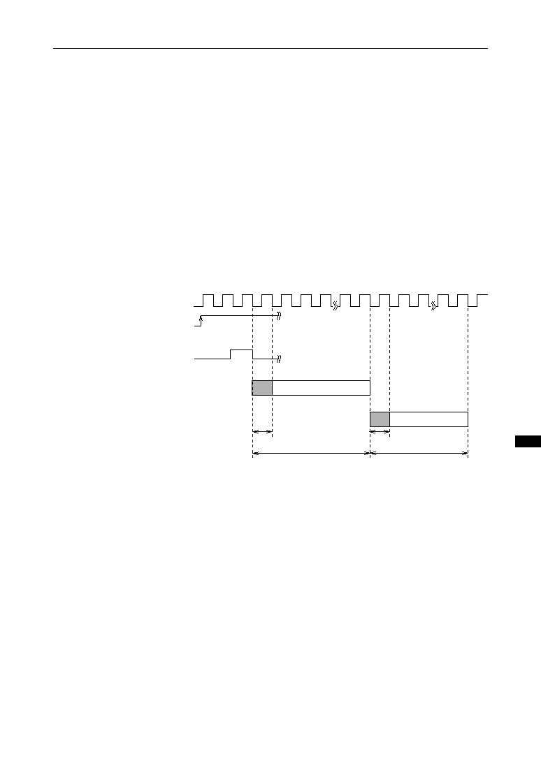
16-29
MSM66591/ML66592 User's Manual
Chapter 16 A/D Converter Functions
16
16.3 Generated Timing of the A/D Hard Select Mode
A/D conversion in the A/D hard select mode is activated 1 CLK after the interrupt
request flag (IRQF) is set in synchronization with the first M1S1 signal following the
generation of any peripheral event (matching, overflow, etc.).
[1]
Activation of Multiple A/D Conversions after Generation of an Interrupt Request
An outline of operation is shown below for the case when the A/D hard select mode is
activated with the same trigger for ch0 and ch1.
When A/D hard select modes of different priority levels (ch0, ch1) are activated by the
same edge, A/D conversion of the higher priority ch0 begins 1 clock after the M1S1
signal, and A/D conversion of the lower priority ch1 begins 1 clock after completion of
the ch0 conversion.
Shaded areas of the figure below indicate dummy cycles required for the start of
conversion.
Master clock (CLK)
Interrupt request generation
(valid edge)
First M1S1 after generation
of valid edge
Hard select mode ch0
Hard select mode ch1
1 clock
ch0 A/D conversion
ch1 A/D conversion
t ch0
t ch1
1 clock
Completion
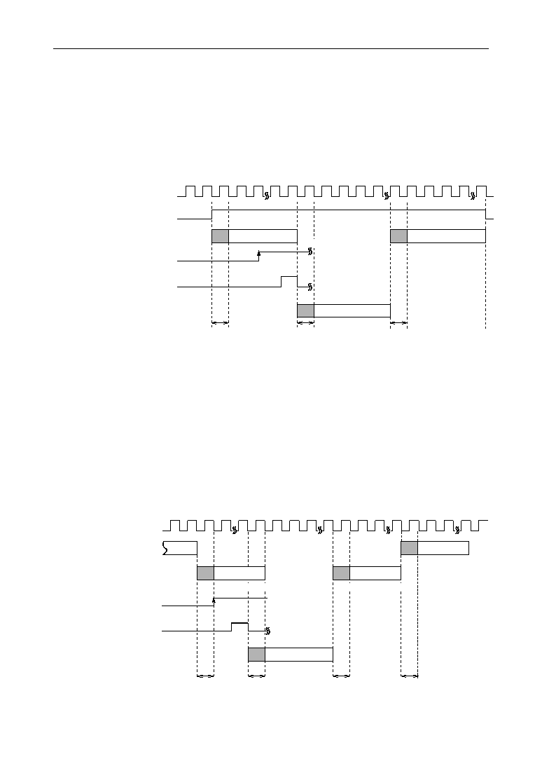
16-30
MSM66591/ML66592 User's Manual
Chapter 16 A/D Converter Functions
[3]
Activation of Hard Select Mode during Select Mode Operation Where Select Mode Was
Activated during Scan Mode Operation
When the select mode is activated during scan mode operation, the scan mode is
immediately suspended and 1 clock later, A/D conversion in the select mode begins. If
an activation request for the hard select mode is generated during operation of that
select mode, the select mode is suspended and 1 clock after the first M1S1 signal
following generation of the activation request, A/D conversion in the hard select mode
begins. After completion of A/D conversion in the hard select mode, A/D conversion in
the suspended select mode is resumed. And 1 clock after completion of the A/D
conversion in the select mode, A/D conversion in the suspended scan mode is re-
sumed.
Master clock (CLK)
Select mode
Scan mode
Suspend
Select mode
Scan mode
Resume
Scan mode
Select mode
Interrupt request generation
(valid edge)
Hard select mode
Hard select mode
Completion
1 clock
1 clock
1 clock
1 clock
First M1S1 after generation
of valid edge
Suspend
Resume
Completion
[2]
Activation of Hard Select Mode A/D Conversion during Select Mode Operation
When the valid edge for the hard select mode occurs during select mode operation, the
select mode is suspended and 1 clock after the first M1S1 signal following generation of
the activation request, A/D conversion in the hard select mode is activated. After
completion of A/D conversion in the hard select mode, A/D conversion in the sus-
pended select mode is resumed.
Master clock (CLK)
STS flag of ADCONnH (n = 0, 1)
Select mode
Interrupt request generation
(valid edge)
First M1S1 after generation
of valid edge
Select mode A/D conversion
Hard select mode
Hard select mode A/D conversion
Select mode A/D conversion
Completion
Completion
1 clock
1 clock
1 clock
Resume
Suspend

16-31
MSM66591/ML66592 User's Manual
Chapter 16 A/D Converter Functions
16
[4]
Hard Select Mode Contention
a) ch1 (low priority) request is generated after ch0 (high priority) activation
When a low priority hard select mode activation request is generated during A/D
conversion in a high priority hard select mode, the request is placed on hold. A/D
conversion in the low priority hard select mode will begin 1 clock after the A/D conver-
sion in the high priority hard select mode is completed.
Master clock (CLK)
Interrupt request generation
(valid edge ch0)
First M1S1 after generation
of valid edge
Hard select mode ch0
Hard select mode ch1
1 clock
ch0 A/D conversion
ch1 A/D conversion
1 clock
Interrupt request generation
(valid edge ch1)
Completion
Completion
b) ch0 (high priority) request is generated after ch1 (low priority) activation
When a high priority hard select mode activation request is generated during A/D
conversion in a low priority hard select mode, the low priority hard select mode is
suspended and 1 clock after the first M1S1 signal following generation of the activation
request, A/D conversion begins in the high priority hard select mode.
1 clock after completion of that A/D conversion, A/D conversion in the suspended low
priority hard select mode is resumed.
Master clock (CLK)
Interrupt request generation
(valid edge ch1)
First M1S1 after generation
of valid edge
Interrupt request generation
(valid edge ch0)
Hard select mode ch0
ch0 A/D conversion
Suspend
Completion
1 clock
1 clock
Hard select mode ch1
ch1 A/D conversion
Completion
1 clock
ch1 A/D conversion

16-32
MSM66591/ML66592 User's Manual
Chapter 16 A/D Converter Functions

Transition Detector
Functions
Chapter 17
17

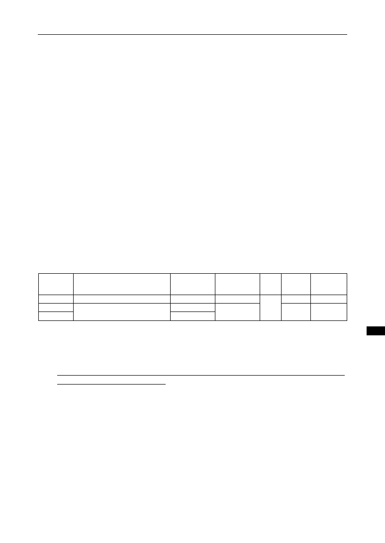
17-1
MSM66591/ML66592 User's Manual
Chapter 17 Transition Detector Functions
17
Table 17-1 Transition Detector Control SFRs
16
R/W
016E
TRNS Control Register
TRNSCON
0000
016F
004F
Transition Detector
--
00
[Note] Addresses above are not consecutive.
8
--
--
TRNSIT
Address [H]
Name
Abbreviated
Name (BYTE)
R/W
8/16-Bit
Operation
Reset
State [H]
Abbreviated
Name (WORD)
17.1 Transition Detector Control Register (TRNSCON)
TRNSCON is an 16-bit register that specifies the valid edges for TRNS0≠TRNS7 pins.
Since only 16-bit data is accessible to TRNSCON, bit manipulation instructions such as
SB and RB can not be executed.
At reset (when the
RES
signal is input, the BRK instruction is executed, the watchdog
timer is overflown, or an operation code trap is generated), TRNSCON becomes
0000H, and the falling edge is specified as the valid edge.
Figure 17-1 shows the configuration of TRNSCON (low-order bits), and Figure 17-2
shows the configuration of TRNSCON (high-order bits).
17. Transition Detector Functions
The MSM66591/ML66592 have eight transition detector functions, which detect the
valid edges (rise, fall, both edges) of an input pin.
If the valid edge specified by TRNSCON is input to TRNS0≠TRNS7 pins, the corre-
sponding bit 0 to bit 7 of the transition detector (TRNSIT) is set to "1". Reset the bit of
TRNSIT to "0" by the program.
TRNS0≠TRNS7 pins are assigned as secondary functions of P4_0≠P4_7 of Port 4.
Therefore the corresponding bit of the Port 4 secondary function control register must
be set to "1" to access the transition detector function.
At reset (when the
RES
signal is input, the BRK instruction is executed, the watchdog
timer is overflown, or an operation code trap is generated), TRNSIT becomes 00H.
If the secondary function of Port 4 is selected, TRNSIT may become undefined, de-
pending on the status of TRNS0≠TRNS7 pins. When using transition detector functions,
set the Port 4 secondary function control register to "1", and then reset the correspond-
ing bit of TRNSIT to "0".
Table 17-1 lists the transition detector control SFRs.
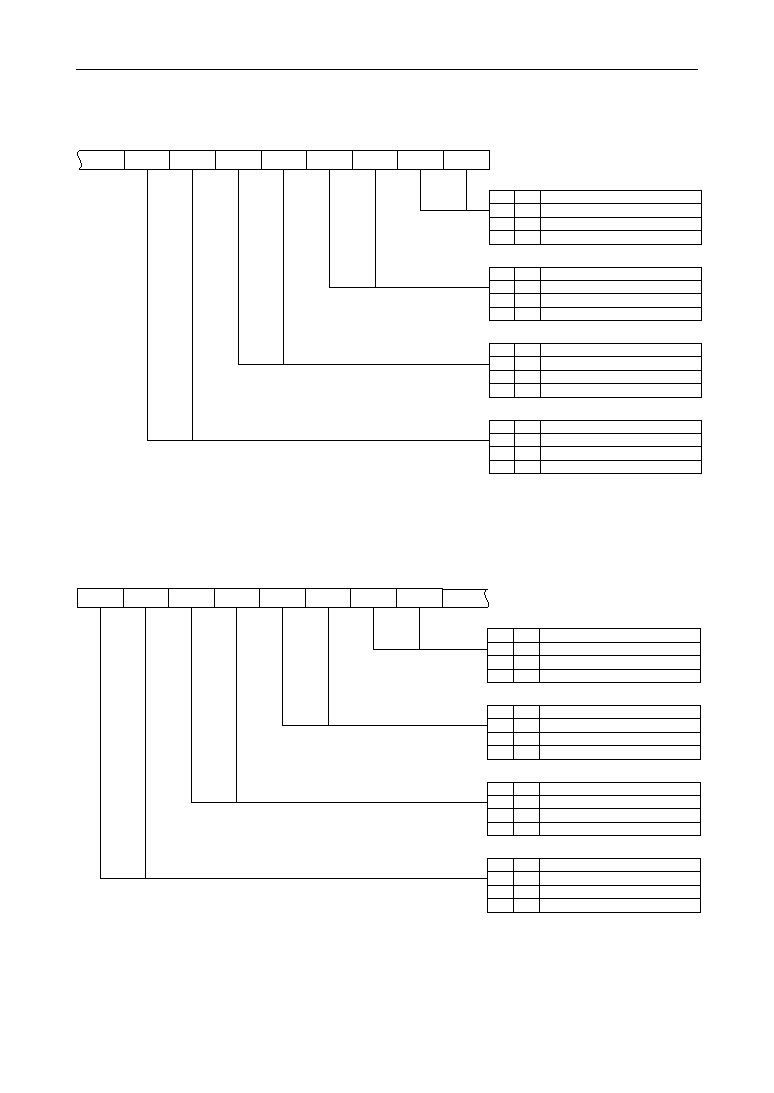
17-2
MSM66591/ML66592 User's Manual
Chapter 17 Transition Detector Functions
Figure 17-1 Configuration of TRNSCON (low-order bits)
Figure 17-2 Configuration of TRNSCON (high-order bits)
6
5
4
3
2
1
0
"*" indicates either "0" or "1".
Valid edge of TRNS0
1
0
0
*
Falling edge
1
0
Rising edge
1
1
Both edges
Valid edge of TRNS1
3
2
0
*
Falling edge
1
0
Rising edge
1
1
Both edges
Valid edge of TRNS2
5
4
0
*
Falling edge
1
0
Rising edge
1
1
Both edges
Valid edge of TRNS3
7
6
0
*
Falling edge
1
0
Rising edge
1
1
Both edges
7
TRNSCON (bits 0≠7)
13
12
11
10
9
8
"*" indicates either "0" or "1".
Valid edge of TRNS4
1
0
0
*
Falling edge
1
0
Rising edge
1
1
Both edges
Valid edge of TRNS5
3
2
0
*
Falling edge
1
0
Rising edge
1
1
Both edges
Valid edge of TRNS6
5
4
0
*
Falling edge
1
0
Rising edge
1
1
Both edges
Valid edge of TRNS7
7
6
0
*
Falling edge
1
0
Rising edge
1
1
Both edges
14
15
TRNSCON (bits 8≠15)
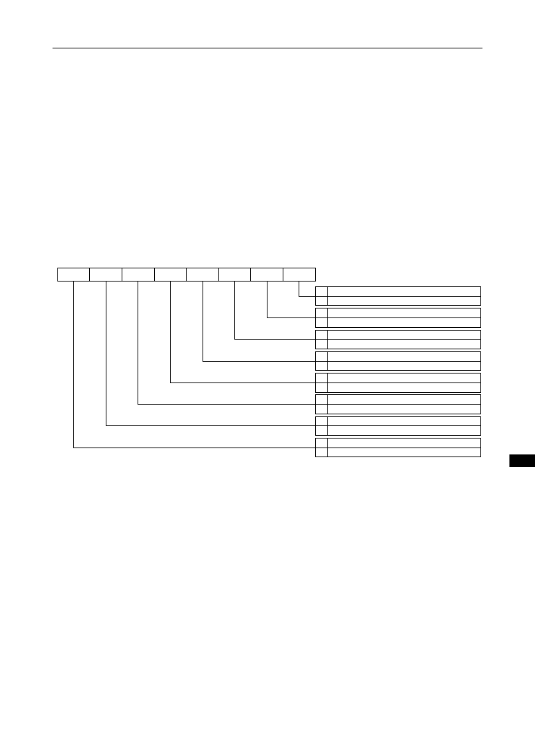
17-3
MSM66591/ML66592 User's Manual
Chapter 17 Transition Detector Functions
17
17.2 Transition Detector Register (TRNSIT)
TRNSIT is an 8-bit register that indicates that the valid edge specified by TRNSCON
has been input to a TRNS pin.
At reset (when the
RES
signal is input, the BRK instruction is executed, the watchdog
timer is overflown, or an operation code trap is generated), TRNSIT becomes 00H.
If the secondary function of Port 4 is selected, TRNSIT may become undefined, de-
pending on the status of the TRNS0≠TRNS7 pins. When using the transition detector,
set the Port 4 secondary function control register to "1", and then reset the correspond-
ing bit of TRNSIT to "0".
Figure 17-3 shows the configuration of TRNSIT.
TRNSF7 TRNSF6 TRNSF5 TRNSF4 TRNSF3 TRNSF2 TRNSF1 TRNSF0
7
6
5
4
3
2
1
0
0 Valid edge not input to TRNS0 pin
1 Valid edge input to TRNS0 pin
0 Valid edge not input to TRNS1 pin
1 Valid edge input to TRNS1 pin
0 Valid edge not input to TRNS2 pin
1 Valid edge input to TRNS2 pin
0 Valid edge not input to TRNS3 pin
1 Valid edge input to TRNS3 pin
0 Valid edge not input to TRNS4 pin
1 Valid edge input to TRNS4 pin
0 Valid edge not input to TRNS5 pin
1 Valid edge input to TRNS5 pin
"--" indicates a bit that is not provided.
"1" is read if a read instruction is executed.
TRNSIT
0 Valid edge not input to TRNS6 pin
1 Valid edge input to TRNS6 pin
0 Valid edge not input to TRNS7 pin
1 Valid edge input to TRNS7 pin
Figure 17-3 Configuration of TRNSIT

17-4
MSM66591/ML66592 User's Manual
Chapter 17 Transition Detector Functions

Peripheral Functions
Chapter 18
18


18-1
18
MSM66591/ML66592 User's Manual
Chapter 18 Peripheral Functions
18. Peripheral Functions
The MSM66591/ML66592 have the following three functions for use in a peripheral IC.
A. clockout function
B.
RES
pin valid level detection function
C.
OE
pin monitor function
18.1 Clockout Function
The clockout function outputs the divided master clock of the MSM66591/ML66592
from the CLKOUT pin (secondary function of P5_6). The dividing ratio of the master
clock is specified by the low-order 3 bits (bits 0, 1, 2) of the peripheral control register
(PRPHF). There are six types of dividing ratios: 2/3, 1/2, 1/3, 1/4, 1/8, and 1/16 of the
master clock. The master clock (CLK) is the frequency generated by multiplying the
original oscillation clock by 2. 2/3 CLK is only available in the MSM66591.
If the CLKOUT pin is used, bit 6 of the Port 5 secondary function control register must
be set to "1".
18.2
RES
Pin Valid Level Detection Function
The
RES
pin valid level detection function is a flag that is set to "1" when the
RES
pin
becomes "L" level, and is assigned to bit 6 (VBFF) of PRPHF. VBFF is reset to "0" by
the program only. Setting VBFF to "1" by the program is invalid.
18.3
OE
Pin Monitor Function
The
OE
pin monitor function is a flag (OERD) that constantly monitors the input level of
the
OE
pin (pin 71), and is assigned to bit 7 of PRPHF.
If OERD is read, the level of the
OE
pin is read. Writing to OERD is invalid.
Figure 18-1 shows the configuration of PRPHF.
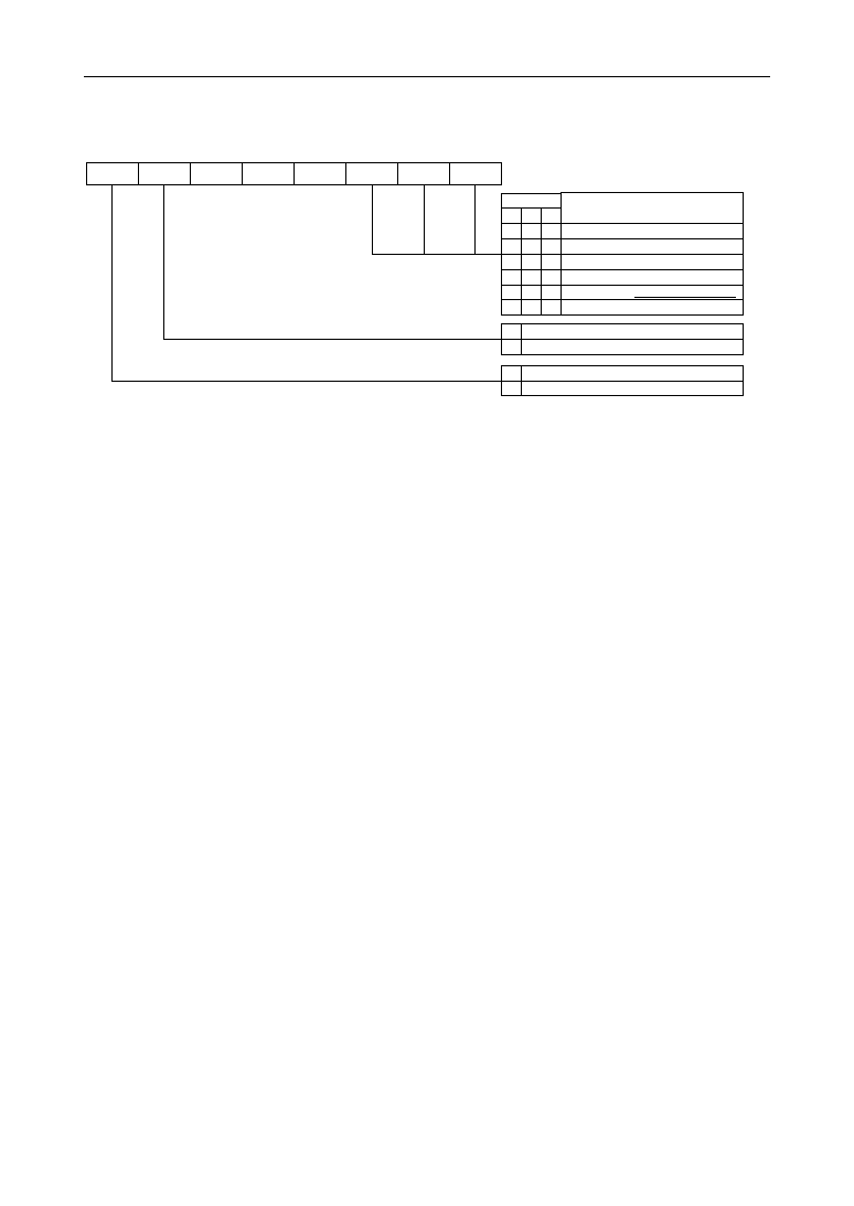
18-2
MSM66591/ML66592 User's Manual
Chapter 18 Peripheral Functions
Figure 18-1 Configuration of PRPHF
OERD
VBFF
--
--
--
CKOUT2 CKOUT1 CKOUT0
7
6
5
4
3
2
1
0
CKOUT
CLKOUT Pin Output Clock
2
0
1/2 CLK
0
1/4 CLK
0
1/8 CLK
0
1/16 CLK
0
RES pin did not become "L" level
1
RES pin became "L" level
0
OE pin "L" level
1
OE pin "H" level
1
2/3 CLK (MSM66591 only)
1
1/3 CLK
*
*
1
0
0
1
1
0
1
0
0
1
0
1
"--" indicates a bit that is not provided.
"1" is read if a read instruction is executed.
"*" indicates either "0" or "1".
PRPHF

External Interrupt Request
Function
Chapter 19
19


19-1
19
MSM66591/ML66592 User's Manual
Chapter 19 External Interrupt Request Function
19. External Interrupt Request Function
The MSM66591/ML66592 have four inputs for external interrupt requests, which can be
classified into two types. One type is a maskable interrupt, and there are three (INT0,
INT1, INT2). The other type is a nonmaskable interrupt, and there is one (NMI).
INT0 and INT1 are assigned as secondary functions of P6_0 and P6_1 of Port 6
respectively. INT2 is assigned as a secondary function of P5_5 of Port 5. If INT0, INT1,
and INT2 are used, set the corresponding bit of the Port 6 secondary function control
register to "1".
A dedicated pin (pin 1) is provided for NMI.
The valid edge of INT0, INT1, and INT2 can be specified using the external interrupt
control register (EXICON).
The valid edge of NMI can be specified using the NMI control register (NMICON).
At reset (when the
RES
signal is input, the BRK instruction is executed, the watchdog
timer is overflown, or an operation code trap is generated), EXICON becomes C0H,
and "L" level is specified as the valid edge of the INT0, INT1, and INT2 pins. Also,
NMICON becomes 3CH or BCH, depending on the state of the NMI pin at reset, and
the fall is specified as the valid edge of the NMI pin.
Figure 19-1 shows the configuration of EXICON. Figure 19-2 shows the configuration of
NMICON.
Bit 7 of NMICON monitors the NMI pin, and bit 6 is an MIPF that enables or disables all
maskable interrupt priorities.
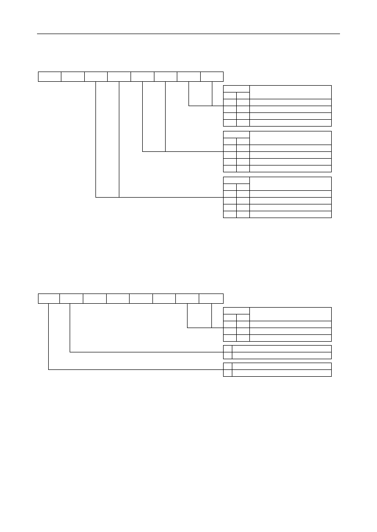
19-2
MSM66591/ML66592 User's Manual
Chapter 19 External Interrupt Request Function
--
--
EX2M1 EX2M0 EX1M1 EX1M0 EX0M1 EX0M0
7
6
5
4
3
2
1
0
EX0M
Valid Edge of INT0
1
0
0
0
"L" level
0
1
Falling edge
1
0
Rising edge
1
1
Both edges
EX1M
Valid Edge of INT1
1
0
0
0
"L" level
0
1
Falling edge
1
0
Rising edge
1
1
Both edges
"--" indicates a bit that is not provided.
"1" is read if a read instruction is executed.
EXICON
EX2M
Valid Edge of INT2
1
0
0
0
"L" level
0
1
Falling edge
1
0
Rising edge
1
1
Both edges
Figure 19-1 Configuration of EXICON
Figure 19-2 Configuration of NMICON
NMIRD MIPF
--
--
--
--
NMIM1 NMIM0
7
6
5
4
3
2
1
0
NMIM
Valid Edge of NMI
1
0
0
* Falling edge
1
0 Rising edge
1
1 Both edges
0 NMI pin "L" level
1 NMI pin "H" level
"--" indicates a bit that is not provided.
"1" is read if a read instruction is executed.
"*" indicates either "0" or "1".
Writing to bit 7 is invalid.
NMICON
0 Maskable interrupt priority: invalid
1 Maskable interrupt priority: valid

Interrupt Request Processing
Function
Chapter 20
20

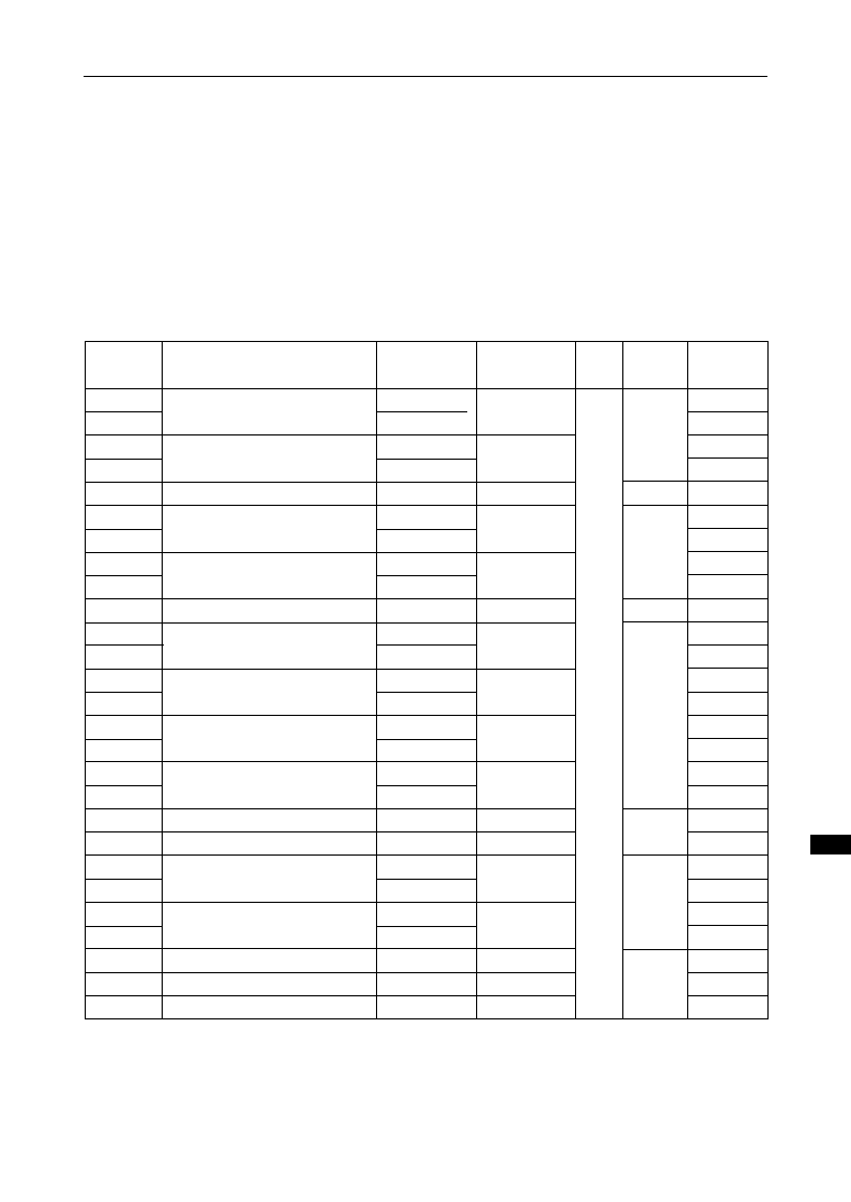
20-1
20
MSM66591/ML66592 User's Manual
Chapter 20 Interrupt Request Processing Function
20. Interrupt Request Processing Function
The MSM66591/ML66592 have 67 types of interrupt causes (external 4, internal 63),
which are assigned to 39 vectors. One external interrupt is nonmaskable. Also four
levels of interrupt priorities can be set for maskable interrupts.
Table 20-1 lists the interrupt control SFRs.
Table 20-1 Interrupt Control SFRs
0040
0041
IRQ0
0042
0043
IRQ1
0044
0046
--
C0
0047
0048
IE0
0049
004A
0140
0141
IE1
0142
0143
IP00
0144
0145
IP01
0146
0147
IP10
0148
0149
IP11
0150
--
0151
--
R/W
8/16
Interrupt Request Register 2
Interrupt Enable Register 0
Interrupt Priority Control
Register 01
Interrupt Priority Control
Register 10
Interrupt Priority Control
Register 11
3C or BC
C0
C0
00
00
00
00
00
00
00
00
C0
00
00
00
00
C0
00
00
00
00
Interrupt Request Register 1
Interrupt Enable Register 1
Interrupt Priority Control
Register 00
NMI Control Register
External Interrupt Control Register
IRQ0L
IRQ0H
IRQ1L
IRQ1H
IRQ2L
IE0L
IE0H
IE1L
IE1H
IP00L
IP00H
IP01L
IP01H
IP10L
IP10H
IP11L
IP11H
NMICON
EXICON
8
8/16
8
--
Interrupt Enable Register 2
IE2L
8
8/16
Interrupt Priority Control Register 20
IP20L
--
Interrupt Priority Control Register 21
IP21L
--
8
IRQD0
Interrupt Request Flag
Disable Register 0
00
00
IRQD0L
IRQD0H
0152
0153
IRQD1
Interrupt Request Flag
Disable Register 1
00
00
IRQD1L
IRQD1H
8/16
0154
0109
014A
Interrupt Request Flag Disable Register 2
C0
IRQD2L
--
Some addresses are not consecutive.
Addresses in the address column marked by "" indicate that the register has bits missing.
Interrupt Request Register 0
Address [H]
Name
Abbreviated
Name (BYTE)
R/W
8/16-Bit
Operation
Reset
State [H]
Abbreviated
Name (WORD)

20-2
MSM66591/ML66592 User's Manual
Chapter 20 Interrupt Request Processing Function
20.1 Non-maskable Interrupt (NMI)
An NMI cannot be masked at all. If the specified valid edge is detected by bit 0 and 1 of
NMICON, the CPU immediately starts the NMI interrupt process.
The only exception when an NMI is masked is for the period of time until execution of
the first instruction is finished after reset (when the
RES
signal is input, the BRK instruc-
tion is executed, the watchdog timer is overflown, or an operation code trap is gener-
ated).
After reset this function prevents the possibility of an NMI being accepted before the
system stack pointer (SSP) value becomes the appropriate value.
By inputting an instruction to set the SSP value as the appropriate value to the first
instruction after reset using the program, the possibility of an NMI before the SSP value
becomes the appropriate value is eliminated.
If an NMI is generated, the hardware automatically performs a series of processes,
which include:
∑ Saving program counter (PC)
∑ Saving accumulator (ACC)
∑ Saving local register base (LRB)
∑ Saving program status word (PSW)
∑ Resetting the NMI request flag
∑ Disabling maskable interrupt acceptance
∑ Disabling multiple interrupt by the NMI itself
∑ Loading value written to vector tables (0008H, 0009H) to the program counter, then
executing the first instruction of the NMI process.
Fourteen cycle are required to shift to each of these NMI process. However, if the
program memory space is extended to 128K bytes (MSM66591) or 192K bytes
(ML66592) by setting bit 1 (LROM) of MEMSCON to "1", 17 cycles are required be-
cause cycles required to save the code segment register (CSR) are added.
An RTI instruction is needed at the end of the NMI interrupt routine.
If the RTI instruction is executed, the hardware automatically performs a series of
processes, which include:
∑ Restoring program status word (PSW)
∑ Restoring local register base (LRB)
∑ Restoring accumulator (ACC)
∑ Restoring program counter (PC)
∑ Clearing disabling maskable interrupt acceptance
∑ Clearing disabling multiple interrupt by the NMI itself
then ending the NMI routine.
Figure 20-1 shows examples of saving and restoring PC, ACC, LRB and PSW.

20-3
20
MSM66591/ML66592 User's Manual
Chapter 20 Interrupt Request Processing Function
∑ At INT (Program memory space is 64K bytes)
(After saving)
(Before RTI execution)
07F7H
07F8H
07F9H
07FAH
07FBH
07FCH
07FDH
07FEH
07FFH
07F7H
07F8H
07F9H
07FAH
07FBH
07FCH
07FDH
07FEH
07FFH
PSWL
PSWH
LRBL
LRBH
ACCL
ACCH
PCL
PCH
07F7H
07F8H
07F9H
07FAH
07FBH
07FCH
07FDH
07FEH
07FFH
PSWL
PSWH
LRBL
LRBH
ACCL
ACCH
PCL
PCH
SSP
SSP
SSP
(Before saving)
(After RTI execution)
(After saving)
(Before RTI execution)
07F5H
07F6H
07F7H
07F8H
07F9H
07FAH
07FBH
07FFH
07F7H
07F8H
07F9H
07FAH
07FBH
07FCH
07FDH
07FFH
PSWH
LRBL
LRBH
ACCL
ACCH
CSR
Undefined
PCH
07F7H
07F8H
07F9H
07FAH
07FBH
07FCH
07FDH
07FFH
PSWH
LRBL
LRBH
ACCL
ACCH
CSR
Undefined
PCH
SSP
SSP
SSP
(Before saving)
(After RTI execution)
07FCH
07FDH
07FEH
07FEH
PCL
07FEH
PCL
07F6H
PSWL
07F6H
PSWL
07F5H
07F5H
∑ At INT (Program memory space is 128K bytes)
Figure 20-1 Examples of Saving and Restoring PC, ACC, LRB, and PSW
[Note] If the program memory space is extended to 128K bytes (MSM66591) or 192K
bytes (ML66592) by setting bit 1 (LROM) of MEMSCON to "1", the code segment
register (CSR), in addition to the above registers, is saved and restored.

20-4
MSM66591/ML66592 User's Manual
Chapter 20 Interrupt Request Processing Function
20.2 Maskable Interrupt
A maskable interrupt is generated by various causes such as internal peripheral
hardware and external pin inputs.
A maskable interrupt is controlled by:
q
Register (IRQD) that enables/disables IRQ flag to be set to "1" by the interrupt
request generated by each factor.
w
Register (IRQ) that is set to "1" by the interrupt request generated by each cause,
that is enabled by IRQD.
e
Register (IE) that enables/disables the interrupt provided by each cause.
r
Flag (MIE) that enables/disables generation of all maskable interrupts.
t
Flag (MIPF) that enables/disables all priorities.
y
Register (IPX0, IPX1) that sets the priority level.
Figure 20-2 shows a conceptual diagram of maskable interrupt control.
Table 20-2 lists the vector addresses and bit symbols for maskable interrupts.
Figure 20-2 Conceptual Diagram of Maskable Interrupt Control
Dxxx
Exxx
MIE
MIPF
PX0xxx PX1xxx
Qxxx
Interrupt cause
generation
source
LV3
LV2
LV1
LV0
NP
Priority
Controller
Dyz
Eyz
MIE
MIPF
PX0yz
PX1yz
Qyz
Interrupt cause
generation
source Z
LV3
LV2
LV1
LV0
NP
Priority
Controller
Interrupt cause
generation
source Y
LEyyy
LEzzz
LQyyy
LQzzz
[One interrupt vector for two interrupt cause]
[One interrupt vector for one interrupt cause]
: The sources included in a dotted box exist in each functional block.
LV3: Level 3
LV2: Level 2
LV1: Level 1
LV0: Level 0
NP: No priority
20-5
20
MSM66591/ML66592 User's Manual
Chapter 20 Interrupt Request Processing Function
Table 20-2 Vector Addresses and Bit Symbols for Maskable Interrupts
0 External interrupt 0 (INT0)
1 TM0 overflow
2 TM1 overflow
3 CAP0 event generation
4 CAP1 event generation
5 CAP2 event generation
6 CAP3 event generation
7 Double-buffer RTO4 event generation
8 Double-buffer RTO5 event generation
9 Double-buffer RTO6 event generation
10 Double-buffer RTO7 event generation
11 Double-buffer RTO8 event generation
12 Double-buffer RTO9 event generation
13 Double-buffer RTO10 event generation
14 Double-buffer RTO11 event generation
15 Serial port 1 transmit/receive ready
16 S0TM/S1TM/S2TM/S3TM/S4TM overflow
17 GTMC/GEVC overflow
18
A/D1 scan/select/hard select conversion
completed
19
A/D0 scan/select/hard select conversion
completed
20 PWC0/PWC1 underflow, or matching
21 PWC2/PWC3 underflow, or matching
22 Serial port 0 transmit/receive ready
23 External interrupt 1 (INT1)
IRQD
DINT0
DTM0OV
DTM1OV
DCAP0
DCAP1
DCAP2
DCAP3
DRTO4
DRTO5
DRTO6
DRTO7
DRTO8
DRTO9
DRTO10
DRTO11
DSCI1
DSTMOV
DGTMOV
DAD1
DAD0
DPW01
DPW23
DSCI0
DINT1
000A
000C
000E
0010
0012
0014
0016
0018
001A
001C
001E
0020
0022
0024
0026
0028
002A
002C
002E
0030
0032
0034
0036
0038
bit
Interrupt Cause
Vector
Address [H]
QINT0
QTM0OV
QTM1OV
QCAP0
QCAP1
QCAP2
QCAP3
QRTO4
QRTO5
QRTO6
QRTO7
QRTO8
QRTO9
QRTO10
QRTO11
QSCI1
QSTMOV
QGTMOV
QAD1
QAD0
QPW01
QPW23
QSCI0
QINT1
IRQ
P0INT0
P0TM0OV
P0TM1OV
P0CAP0
P0CAP1
P0CAP2
P0CAP3
P0RTO4
P0RTO5
P0RTO6
P0RTO7
P0RTO8
P0RTO9
P0RTO10
P0RTO11
P0SCI1
P0STMOV
P0GTMOV
P0AD1
P0AD0
P0PW01
P0PW23
P0SCI0
P0INT1
IPX0
IE
EINT0
ETM0OV
ETM1OV
ECAP0
ECAP1
ECAP2
ECAP3
ERTO4
ERTO5
ERTO6
ERTO7
ERTO8
ERTO9
ERTO10
ERTO11
ESCI1
ESTMOV
EGTMOV
EAD1
EAD0
EPW01
EPW23
ESC10
EINT1
P1INT0
P1TM0OV
P1TM1OV
P1CAP0
P1CAP1
P1CAP2
P1CAP3
P1RTO4
P1RTO5
P1RTO6
P1RTO7
P1RTO8
P1RTO9
P1RTO10
P1RTO11
P1SCI1
P1STMOV
P1GTMOV
P1AD1
P1AD0
P1PW01
P1PW23
P1SCI0
P1INT1
IPX1
24 Double-buffer RTO12 event generation
25 Double-buffer RTO13 event generation
26 PWC4/PWC5 underflow, or matching
DRTO12
DRTO13
DPW45
003A
003C
003E
QRTO12
QRTO13
QPW45
P0RTO12
P0RTO13
P0PW45
ERTO12
ERTO13
EPW45
P1RTO12
P1RTO13
P1PW45
27 PWC6/PWC7 underflow, or matching
DPW67
0040
QPW67
P0PW67
EPW67
P1PW67
28 CAP 14 event generation
DCAP14
0042
QCAP14
P0CAP14
ECAP14
P1CAP14
29 CAP 15 event generation
DCAP15
0044
QCAP15
P0CAP15
ECAP15
P1CAP15
30 Flexible timer 16 event generation
DFTM16
0046
QFTM16
P0FTM16
EFTM16
P1FTM16
31 Flexible timer 17 event generation
DFTM17
0048
QFTM17
P0FTM17
EFTM17
P1FTM17
32 PWC8/PWC9 underflow, or matching
DPW89
006A
QPW89
P0PW89
EPW89
P1PW89
33 PWC10/PWC11 underflow, or matching
DPW1011
006C
QPW1011
P0PW1011
EPW1011
P1PW1011
34 Serial port 2 transmit/receive ready
DSCI2
006E
QSCI2
P0SCI2
ESCI2
P1SCI2
35 Serial port 3 transmit/receive ready
DSCI3
0070
QSCI3
P0SCI3
ESCI3
P1SCI3
36 Serial port 4 transmit/receive ready
DSCI4
0072
QSCI4
P0SCI4
ESCI4
P1SCI4
37
SIO5 event generation,
externali nterrupt (INT2)
DSCI5
0074
QSCI5
P0SCI5
ESCI5
P1SCI5

20-6
MSM66591/ML66592 User's Manual
Chapter 20 Interrupt Request Processing Function
[1]
Interrupt Request Flag Disable Register IRQD (IRQD0L, IRQD0H, IRQD1L, IRQD1H, IRQD2L)
The IRQD is a register that enables/disables the corresponding bit of the IRQ to be set
to "1" by the interrupt signal from each interrupt generation source. If a bit of IRQD is
"1", the corresponding bit of IRQ is not set, even if the corresponding interrupt genera-
tion source generated an interrupt request. If a bit of IRQD is "0", the corresponding bit
of IRQ is set to "1" by the interrupt request from the corresponding interrupt generation
source.
At reset (when the
RES
signal is input, the BRK instruction is executed, the watchdog
timer is overflown, or an operation code trap is generated), IRQD0L, IRQD0H, IRQD1L,
and IRQD1H become 00H, IRQD2L becomes C0H, and enable the corresponding bit of
IRQ to be set to "1" by an interrupt signal from each interrupt generation source.
[2]
Interrupt Request Register IRQ (IRQ0L, IRQ0H, IRQ1L, IRQ1H, IRQ2L)
IRQ becomes "1" synchronizing with the M1S1 signal if an interrupt signal is generated
from each interrupt generation source enabled by IRQD, and becomes "0" automatically
during an interrupt transition cycle if an interrupt is accepted.
A bit of IRQ can be set to "1" or "0" by the program.
At reset (when the
RES
signal is input, the BRK instruction is executed, the watchdog
timer is overflown, or an operation code trap is generated), IRQ0L, IRQ0H, IRQ1L, and
IRQ1H become 00H, and IRQ2L becomes C0H.
[3]
Interrupt Enable Register IE (IE0L, IE0H, IE1L, IE1H, IE2L)
The IE is a register that specifies an interrupt generation enable/disable independently.
If a bit of IE is "0", the corresponding interrupt generation is disabled. If a bit of IE is "1",
the corresponding interrupt generation is enabled.
At reset (when the
RES
signal is input, the BRK instruction is executed, the watchdog
timer is overflown, or an operation code trap is generated), IE0L, IE0H, IE1L, and IE1H
become 00H, and IE2L becomes C0H.
[4]
Master Interrupt Enable Flag (MIE)
The MIE is a 1-bit flag on PSW. MIE specifies enable/disable of all maskable interrupt
generation. If MIE is "0", all maskable interrupt generation is disabled. If MIE is "1", the
generation of all independently enabled interrupts are enabled.
[5]
Master Interrupt Priority Flag (MIPF)
The MIPF is a 1-bit flag assigned to bit 6 of NMICON. MIPF specifies valid/invalid of all
maskable interrupt priorities. If MIPF is "0", priority by IPX0 and IPX1 becomes invalid,
and interrupt generation is controlled only by IE and MIE. If MIPF is "1", four types of
priority, level 0≠level 3, are given to all maskable interrupts by IPX0 and IPX1.

20-7
20
MSM66591/ML66592 User's Manual
Chapter 20 Interrupt Request Processing Function
PX1xxx PX0xxx
Priority
0
0
Level 0
0
1
Level 1
1
0
Level 2
1
1
Level 3
(low)
(high)
At reset (when the
RES
signal is input, the BRK instruction is executed, the watchdog
timer is overflown, or an operation code trap is generated), IP00L, IP00H, IP10L,
IP10H, IP01L, IP01H, IP11L, and IP11H become 00H, and IP20L and IP21L become
C0H.
[6]
Interrupt Priority Control Register
IPX0 (IP00L, IP00H, IP10L, IP10H, IP20L), IPX1 (IP01L, IP01H, IP11L, IP11H, IP21L)
As a pair IPX0 and IPX1 specify the priority of maskable interrupts. If the corresponding
bit of IPX0 and IPX1 for a maskable interrupt is PX0xxx and PX1xxx, the priority given
to the maskable interrupt is as follows.

20-8
MSM66591/ML66592 User's Manual
Chapter 20 Interrupt Request Processing Function
20.3 Operation of Maskable Interrupt
When an interrupt request signal is generated, the logic to notify about interrupt request
generation to the judgment logic of an interrupt priority functions as follows:
∑ Interrupt request signal is output from an interrupt generation source.
∑ If the corresponding bit of IRQD is "1", the interrupt request signal is ignored, and
nothing occurs to this interrupt. If the corresponding bit of IRQD is "0", the corre-
sponding IRQ bit becomes "1". The IRQ bit can also be set to "1" by executing a
write instruction.
∑ If either the corresponding IE bit or the MIE on PSW is "0" when the IRQ bit is "1",
interrupt generation wait status occurs. When the IRQ bit is "1", the judgment logic
of an interrupt priority functions if both the corresponding IE bit and the MIE on the
PSW are "1".
The judgment logic of an interrupt priority functions as follows.
∑ If MIPF on PSW is "0", the judgment logic of an interrupt priority does not function,
and an interrupt is immediately generated.
If MIPF on PSW is "1", one of level 0 to level 3 priorities is assigned to the interrupt
according to the corresponding bit of IPX0 and IPX1.
∑ If no interrupt has been executed when an interrupt generation request is sent to the
judgment logic of an interrupt priority, the interrupt is immediately generated.
∑ If one or more interrupts are in execution when an interrupt generation request is
sent to the judgment logic of an interrupt priority, and if the priority of the interrupt to
be requested is higher than the highest priority of the interrupt in execution, the
interrupt is immediately generated.
∑ If one or more interrupts are in execution when an interrupt generation request is
sent to the judgment logic of an interrupt priority, and if the priority of the interrupt to
be requested is the same as or lower than the highest priority of the interrupts in
execution, the interrupt generation wait status occurs.
Process except interrupt
[Note]
If interrupts occur at the same time, the one with the highest priority level has the priority.
If interrupts with the same priority level occur at the same time, the one with the lower interrupt vector
address has the priority.
Level 1 interrupt process
Level 2 interrupt process X:interrupt wait
X:interrupt wait
X:interrupt wait
q:interrupt generated
Level 3 interrupt process X:interrupt wait
X:interrupt wait
X:interrupt wait
X:interrupt wait
NMI process
X:interrupt wait
X:interrupt wait
X:interrupt wait
X:interrupt wait
q:interrupt generated
q:interrupt generated
X:interrupt wait
X:interrupt wait
Level 0 interrupt process
q:interrupt generated
Level 0 Interrupt
Request
Level 1 Interrupt
Request
q:interrupt generated q:interrupt generated
Level 2 Interrupt
Request
q:interrupt generated
Level 3 Interrupt
Request
q:interrupt generated
q:interrupt generated
q:interrupt generated
X:interrupt wait
q:interrupt generated
q:interrupt generated
q:interrupt generated
q:interrupt generated
q:interrupt generated
X:interrupt wait
NMI Request
Generated
Interrupt
Process
in execution

20-9
20
MSM66591/ML66592 User's Manual
Chapter 20 Interrupt Request Processing Function
If a maskable interrupt is generated, the hardware automatically performs a series of
processes, which include:
∑ Saving program counter (PC)
∑ Saving accumulator (ACC)
∑ Saving local register base (LRB)
∑ Saving program status word (PSW)
∑ Resetting IRQ that generated maskable interrupt process
∑ Resetting MIE on PSW (MIE
"0" = acceptance of maskable interrupt disabled)
∑ Storing interrupt priority level (acceptance of interrupt with same or lower level
priority disabled)
∑ Loading value written to vector table to program counter
and then executing the first instruction of a maskable interrupt process.
Fourteen cycles are required to shift to each maskable interrupt process (Interrupt
transition cycle).
However, if the program memory space is 128K bytes (MSM66591) or 192K bytes
(ML66592) by setting bit 1 (LROM) of MEMSCON to "1", 17 cycles are required be-
cause cycles required to save the code segment register (CSR) are added.
When an interrupt generation condition is fulfilled by setting IRQ, IE, IP, or MIPF to "1"
by an instruction, the actual generation of the interrupt occurs after the execution of the
next instruction after the instruction that set the IRQ, IE, IP, or MIPF to "1".
It is necessary to execute an RTI instruction at the end of a maskable interrupt routine.
If an RTI instruction is executed, the hardware automatically performs a series of
processes, which include:
∑ Deleting highest level of stored interrupt priority level
∑ Restoring program status word (PSW) (MIE
"1")
∑ Restoring local register base (LRB)
∑ Restoring accumulator (ACC)
∑ Restoring program counter (PC)
and then ending the maskable interrupt routine.
[Note] If the program memory space is expanded to 128K bytes (MSM66591) or 192K
bytes (ML66592) by setting bit 1 (LROM) of MEMSCON to "1", the code segment
register (CSR) is saved or returned from.
Figure 20-1 (page 20-3) shows examples of saving and restoring PC, ACC, LRB and
PSW.

20-10
MSM66591/ML66592 User's Manual
Chapter 20 Interrupt Request Processing Function

Bus Port Functions
Chapter 21
21


21-1
21
MSM66591/ML66592 User's Manual
Chapter 21 Bus Port Functions
21. Bus Port Functions
The MSM66591/ML66592 can externally expand up to 128K bytes (MSM66591) or
256K bytes (ML66592) of program memory (ROM usually) by setting the
EA
pin to a "L"
level.
The external program memory is accessed using the bus port functions of Port 0 (P0),
Port 1 (P1), and Port 12 (P12_0, P12_1 (ML66592 only)) and the secondary functions
of Port 7 (ALE,
PSEN
).
21.1 Bus Port (P0, P1, P12_0, P12_1) Functions
P0, P1, P12_0 and P12_1 (ML66592 only) have secondary functions as a bus port, in
addition to the primary functions as an I/O port.
P0, P1, P12_0 and P12_1 (ML66592 only) automatically switch their function from a
primary function to a secondary function or vice versa if the
EA
pin is at "L" level.
21.1.1 Operation of P0, P1, P12_0 and P12_1 During a Program Memory Access
When the internal program memory is accessed (
EA
pin is at "H" level), P0, P1, P12_0
and P12_1 operate as an I/O port.
When the external program memory is accessed (
EA
pin is at "L" level), P0 operates as
a port that outputs lower addresses and that inputs instruction. P1, P12_0 and P12_1
(ML66592 only) operate as ports that output higher addresses.
Table 21-1 shows the operation of P0, P1, P12_0 and P12_1 during a program memory
access.
Table 21-1 Operation of P0, P1, P12_0 and P12_1 During a Program Memory Access
Memory
Address
Internal program
Access Target
High-order
address output
Low-order address output,
program data input
EA Pin
External program
Operation of P1,
P12_0, P12_1
*1
Operation of P0
Input/output port
"H" level
"L" level
00000H≠1FFFDH
*2
*1 P12_1 is only for the ML66592.
*2 00000H≠3FFFDH for the ML66592.

21-2
MSM66591/ML66592 User's Manual
Chapter 21 Bus Port Functions
21.2 External Memory Access
21.2.1 External Program Memory Access
The MSM66591 can access a maximum of 128K bytes (00000H≠1FFFDH) of program
memory space using a 16-bit program counter and a 1-bit code segment register
(CSR). When the
EA
pin is low, external program memory is accessed to 00000H≠
1FFFDH.
By using a 16-bit program counter and a 2-bit code segment register (CSR), the
ML66592 can access a maximum of 192K bytes (00000H≠2FFFDH) of program
memory space internally and a maximum of 256K bytes (0000H≠3FFDH) of program
memory space externally. When the
EA
pin is low, external program memory is ac-
cessed to 00000H≠3FFFDH.
The Figure 21-1 shows the external program memory (ROM) connection example.
AD0≠AD7 (P0_0≠P0_7)
(P7_2) ALE
A8≠A16 (P1_0≠P1_7, P12_0)
(P7_3) PSEN
O0≠O7
A0≠A7
A8≠A16
OE
CE
MSM66591
External ROM (128K bytes MAX.)
Latch
Circuit
[Note]
Since in the ML66592 address 17 (A17) is output from the P12_1 pin, connect
the P12_1 pin to A17 of the external ROM. Up to 256K bytes can be accessed.
Figure 21-1 External ROM Connection Example (MSM66591)
21.2.2 External Program Memory Access Timing
Figures 21-2 and 21-3 show external program memory access timing.
The MSM66591/ML66592 have a function to insert a wait cycle when the external
memory access time is slow. (READY function: see 5.2). Use this function according to
the access time of the external memory required for use.
However, unlike access to the internal memory, one cycle is automatically inserted for
every one-byte-access to the external memory.
ROMRDY is a register to specify the number of cycles to be inserted in addition to the
above one cycle.
For actual AC characteristics, see Chapter 25, "Electrical Characteristics."

21-3
21
MSM66591/ML66592 User's Manual
Chapter 21 Bus Port Functions
P7_2/ALE
CLK
P7_3/PSEN
AD0≠AD7
(P0_0≠P0_7)
A8≠A16
(P1_0≠P1_7, P12_0)
PC8≠16
PC0≠7
PC8≠16
INST0≠7
PC0≠7
INST0≠7
[Note] 1 wait cycle is automatically inserted into the CPU in this case as well.
In the ML66592, the timing for A17 (address 17) is the same as A8≠A16.
Figure 21-2 External Program Memory Access Timing (No Wait Cycles)
P7_2/ALE
CLK
P7_3/PSEN
AD0≠AD7
(P0_0≠P0_7)
A8≠A16
(P1_0≠P1_7, P12_0)
PC8≠16
PC0≠7
PC8≠16
INST0≠7
PC0≠7
Number of wait cycles
inserted according to
the ROMRDY setting.
In this example, 2 wait
cycles.
[Note]
3 (= 1 + 2) wait cycles are automatically inserted into the CPU in this case as well.
In the ML66592, the timing for A17 (address 17) is the same as A8≠A16.
Figure 21-3 External Program Memory Access Timing (2 Wait Cycles)

21-4
MSM66591/ML66592 User's Manual
Chapter 21 Bus Port Functions

Expansion Port
Chapter 22
22


22-1
22
MSM66591/ML66592 User's Manual
Chapter 22 Expansion Port
22. Expansion Port
The MSM66591/ML66592 have a 1-channel internal expansion port for the external
expansion of general-purpose ports.
The expansion port expands port functions by outputting parallel data of the internal
registers as synchronous serial data, and by externally converting serial data to parallel
data.
External parallel data can also be input as synchronous serial data and converted to
parallel data internally. Data input and output uses pin P10_6/SFTDAT, the shift clock
output uses pin P10_5/SFTCLK, and the external latch strobe uses pin P10_7/SFTSTB.
The data length is selectable as 8 bits or 16 bits. Connection of devices such as a
74HC165 is assumed for external input and a 74HC595 is assumed for external output
of the expansion port. Because expansion port functions are assigned as secondary
functions of Port 10, corresponding bits of the Port 10 secondary function control
register must be set to "1" to use expansion port functions.
22.1 Expansion Port Configuration
The expansion port consists of a 16-bit shift register that exchanges data with the
exterior, a 16-bit buffer register (EXTPD) for the shift register, EXTPCON to control
operation, and a control circuit.
Figure 22-1 shows the configuration of the expansion port.
Figure 22-1 Expansion Port Configuration
Internal BUS
Shift Register
Control Circuit
EXTPD
EXTPCON
1/4 CLK
P10_6/SFTDAT
P10_5/SFTCLK
P10_7/SFTSTB

22-2
MSM66591/ML66592 User's Manual
Chapter 22 Expansion Port
22.2 Expansion Port Control Register (EXTPCON)
The expansion port control register (EXTPCON) is a 3-bit register that controls the
function of the expansion port.
At reset (when the
RES
signal is input, the BRK instruction is executed, the watchdog
timer is overflown, or an operation code trap is generated), EXTPCON becomes F8H.
Figure 22-2 shows the configuration of EXTPCON.
<Description of Each Bit>
∑ EXPBUSY (bit 0)
This BUSY flag indicates that a data transfer is in progress.
This bit is read-only, and writes are ignored.
∑ DATMOD (bit 1)
This bit specifies the bit length of the data transfer.
If "0", 8 bits of data are transferred. If "1", 16 bits of data are transferred.
∑ IOMOD (bit 2)
This bit specifies the data transfer direction.
If "0", data is input. If "1", data is output.
Figure 22-2 EXTPCON Configuration
EXTPCON
7
6
5
4
3
2
1
0
--
--
--
--
--
IOMODE
DATMODE
EXPBUSY
"--" indicates a bit that is not provided.
"1" is read if a read instruction is executed.
Halted
Data transfer in progress
8-bit mode
16-bit mode
Input mode
Output mode
0
1
0
1
0
1

22-3
22
MSM66591/ML66592 User's Manual
Chapter 22 Expansion Port
22.3 Expansion Port Register (EXTPD)
The expansion port register (EXTPD) is a 16-bit buffer register that exchanges data
with the exterior via the shift register. 8-bit access is also possible for this register,
though only for the lower 8 bits as EXTPDL. Note that if 8-bit data is written to EXTPDL,
data at "00H" will be written to the higher 8 bits of EXTPD.
During the input mode, a data transfer (input) is started by reading this register.
During the output mode, a data transfer (output) is started by writing to this register.
At reset (when the
RES
signal is input, the BRK instruction is executed, the watchdog
timer is overflown, or an operation code trap is generated), EXTPD becomes 0000H.
22.4 Expansion Port Operation
[1]
Input Mode
In the input mode, it is assumed that a 74HC165 or other shift register is connected
externally.
Reading EXPTD causes the transfer (input) to start and the EXPBUSY flag to change
to "1". When EXPTD is read, the latch strobe (SFTSTB) changes to a "L" level.
Next, when the shift clock (SFTCLK) rises, external data (SFTDAT) is input. When
SFTCLK falls, external data is latched internally, and at the same time, SFTSTB
changes to a "H" level. External data changes in sync with the rise of SFTCLK and is
latched internally in sync with the fall of SFTCLK. When SFTCLK outputs 8 clocks, the
transfer (input) is completed, the shift register contents are loaded into EXTPD, and the
EXPBUSY flag changes to "0". SFTCLK is fixed at 1/4 CLK (1/4 of the internal clock).
During the 16-bit mode, SFTCLK outputs 16 clocks and 16-bit transfers are performed.
Figure 22-3 shows the timing of the inputs mode (8-bit mode).
SFTDAT
(shift data)
SFTCLK (1/4 CLK)
(shift clock)
SFTSTB
(data latch)
bit 0
bit 1
bit 2
bit 3
bit 4
bit 5
bit 6
bit 7
Figure 22-3 Input Mode Timing (8-Bit Mode Example)

22-4
MSM66591/ML66592 User's Manual
Chapter 22 Expansion Port
Figure 22-4 Output Mode Timing (8-Bit Mode Example)
SFTDAT
(shift data)
SFTCLK (1/4 CLK)
(shift clock)
SFTSTB
(data latch)
bit 0
bit 1
bit 2
bit 3
bit 4
bit 5
bit 6
bit 7
[2]
Output Mode
In the output mode, it is assumed that a 74HC595 or other shift register is connected
externally.
Writing data to EXPTD causes the transfer (output) to start and the EXPBUSY flag to
change to "1". When data is written to EXPTD, shift data is output in sync with the fall of
the shift clock (SFTCLK). It is assumed that data is captured externally in sync with the
rise of SFTCLK. When SFTCLK outputs 8 clocks, the transfer (output) is completed. At
the same time, SFTSTB changes to a "L" level. 1 shift clock later SFTSTB changes to a
"H" level and data is latched externally. (During this 1 shift clock interval, the shift clock
is not output.) And at the same time that SFTSTB changes to a "H" level, the EXPBUSY
flag becomes "0". SFTCLK is fixed at 1/4 CLK (1/4 of the internal clock).
During the 16-bit mode, SFTCLK outputs 16 clocks and 16-bit transfers are performed.
Figure 22-4 shows the timing of the output mode.

Serial Port with FIFO (SCI5)
Chapter 23
23


23-1
MSM66591/ML66592 User's Manual
Chapter 23 Serial Port with FIFO (SCI5)
23
23. Serial Port with FIFO (SCI5)
The MSM66591/ML66592 have an internal Serial I/O (SCI5) Port with dedicated FIFO
that is used for serial synchronous communication with the CAN controller. SCI5
transmits and receives data in 8-bit units in synchronization with the clock specified by
SCI5 control register 0 (SCI5CON0).
Since an internal 8-stage FIFO functions as a transmit-receive buffer, consecutive
transmission or reception of a maximum of 8 bytes is possible. After data transmission
is completed, an SCI5 interrupt request is generated.
With SCI5, the shift clock for data transfer is output from pin P5_2/SCLK, transmit data
is output from pin P5_1/SDOUT, and receive data is input from pin P5_0/SDIN.
A chip select pin (P5_4/
CS
), a read and write control pin (P5_3/RWB), a WAIT pin
(P5_7/WAIT) with BUSY signal input, and an interrupt input pin (P5_5/INT2) are
provided for use with the CAN controller.
If SCI5 is to be used, set the following pins to their secondary function: P5_0/SDIN,
P5_1/SDOUT, P5_2/SCLK, P5_3/RWB, P5_4/
CS
, P5_5/INT2, and P5_7/WAIT.
23.1 SCI5 Configuration
SCI5 consists of a data buffer FIFO, an 8-bit SFDOUT register that writes to the FIFO,
an 8-bit SFDIN register that reads FIFO data, an 8-bit SFADR register that specifies the
CAN controller address to access, a shift register that performs serial transfers, 8-bit
SCI5CON0 and SCI5CON1 registers that control SCI5 operation, and a control circuit.
Figure 23-1 shows the configuration of SCI5.
Figure 23-1 SCI5 Configuration (Serial I/O with FIFO)
Internal BUS
SCI5CON0
SCI5CON1
SFDIN
Control Circuit
8-byte FIFO
SFDOUT
SFADR
Shift Register
P5_1/SDOUT pin
P5_0/SDIN pin
P5_2/SCLK pin
P5_4/CS pin
P5_3/RWB pin
P5_5/INT2 pin
P5_7/WAIT pin

23-2
MSM66591/ML66592 User's Manual
Chapter 23 Serial Port with FIFO (SCI5)
23.2 SCI5 Control Register 0 (SCI5CON0)
The SCI5 control register 0 (SCI5CON0) is a 7-bit register that controls SCI5 operation.
At reset (when the
RES
signal is input, the BRK instruction is executed, the watchdog
timer is overflown, or an operation code trap is generated), SCI5CON0 becomes 10H.
Figure 23-2 shows the configuration of SCI5CON0.
<Description of Each Bit>
∑ S5CK0≠S5CK2 (bits 0≠2)
These bits select the SCI5 shift clock.
The selected shift clock is output from pin P5_2/SCLK.
∑ S5RES (bit 3)
This flag is used to initialize the SCI5's FIFO pointer.
If this flag is set to "1", the FIFO pointer will be initialized. After initialization, this flag
is automatically cleared. This flag is used to initialize the FIFO pointer when commu-
nication is cut off.
∑ S5EXIE (bit 5)
This flag enables or disables the generation of interrupt requests by the valid edge of
external interrupt 2 (INT2).
If this bit is set to "1", the generation of interrupt requests is enabled. If set to "0", the
generation of interrupt requests is disabled.
∑ S5RIE (bit 6)
This flag enables or disables the generation of interrupt requests at the completion of
SCI5 reception.
If this bit is set to "1", the generation of interrupt requests is enabled. If set to "0", the
generation of interrupt requests is disabled.
∑ S5TIE (bit 7)
This flag enables or disables the generation of interrupt requests at the completion of
SCI5 transmission.
If this bit is set to "1", the generation of interrupt requests is enabled. If set to "0", the
generation of interrupt requests is disabled.
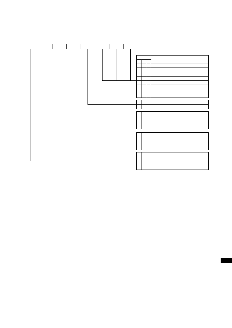
23-3
MSM66591/ML66592 User's Manual
Chapter 23 Serial Port with FIFO (SCI5)
23
Figure 23-2 SCI5CON0 Configuration
SCI5CON0
7
6
5
4
3
2
1
0
S5TIE
S5RIE
S5EXIE
--
S5RES
S5CK2
S5CK1
S5CK0
S5CK
SCI5 shift clock
2 1 0
0 0 0
1/4 CLK
1/8 CLK
1/16 CLK
1/32 CLK
1/2 TBCCLK
1/4 TBCCLK
1/8 TBCCLK
1/16 TBCCLK
0 0 1
0 1 0
0 1 1
1 0 0
1 0 1
1 1 0
1
0
1
0
1
0
1
0
1
Interrupt request due to SCI5 receive
completion: disabled
Interrupt request due to SCI5 receive
completion: enabled
Interrupt request due to SCI5 transmit
completion: disabled
Interrupt request due to SCI5 transmit
completion: enabled
1 1
Normal FIFO operation
FIFO pointer initialization
Interrupt request due to INT2 valid
edge input: disabled
Interrupt request due to INT2 valid
edge input: enabled
"--" indicates a bit that is not provided.
"1" is read if a read instruction is executed.

23-4
MSM66591/ML66592 User's Manual
Chapter 23 Serial Port with FIFO (SCI5)
23.3 SCI5 Control Register 1 (SCI5CON1)
The SCI5 control register 1 (SCI5CON1) is a 6-bit register that controls SCI5 operation.
At reset (when the
RES
signal is input, the BRK instruction is executed, the watchdog
timer is overflown, or an operation code trap is generated), SCI5CON1 becomes C0H.
Figure 23-3 shows the configuration of SCI5CON1.
<Description of Each Bit>
∑ S5RN0≠S5RN3 (bits 0≠3)
These bits specify the number of bytes of receive data during reception.
These bits are ignored during transmission.
∑ TENR (bit 4)
This flag starts reception. Setting this bit to "1" will start reception.
When the number of data bytes specified by S5RN0≠S5RN3 are received, this bit is
automatically cleared.
If this bit is cleared during a reception, the reception is immediately suspended and
SCI5 is initialized.
∑ TENT (bit 5)
This flag starts transmission. Setting this bit to "1" will start transmission.
When the number of data bytes written to the SFDOUT transmit buffer are transmit-
ted, this bit is automatically cleared.
If this bit is cleared during a transmission, the transmission is immediately suspended
and SCI5 is initialized.
Figure 23-3 SCI5CON1 Configuration
SCI5CON1
7
6
5
--
--
TENT
4
3
2
1
0
TENR
S5RN3
S5RN2
S5RN1
S5RN0
3
2
1
0
0
0
0
0
0
0
0
1
0
0
1
0
0
0
1
1
0
1
0
0
0
1
0
1
0
1
1
0
0
1
1
1
1
*
0
1
Reception complete
Start reception
0
1
Transmission complete
Start transmission
*
*
S5RN
Number of
SCI5 receive bytes
Prohibited setting
1 byte
2 bytes
3 bytes
4 bytes
5 bytes
6 bytes
7 bytes
8 bytes
"--" indicates a bit that is not provided.
"1" is read if a read instruction is executed.
"*" indicates either "1" or "0".

23-5
MSM66591/ML66592 User's Manual
Chapter 23 Serial Port with FIFO (SCI5)
23
23.4 SCI5 Interrupt Register (SCI5INT)
The SCI5 interrupt register (SCI5INT) is a 3-bit register that controls SCI5 interrupts.
At reset (when the
RES
signal is input, the BRK instruction is executed, the watchdog
timer is overflown, or an operation code trap is generated), SCI5INT becomes 1FH.
Figure 23-4 shows the configuration of SCI5INT.
<Description of Each Bit>
∑ S5EXIRQ (bit 5)
When a valid edge is input to external interrupt 2 (INT2), this individual interrupt
request flag becomes "1".
Because this flag is not automatically cleared even when an interrupt is processed, it
must be cleared by the program.
∑ S5RIRQ (bit 6)
When SCI5 reception is complete, this individual interrupt request flag becomes "1".
Because this flag is not automatically cleared even when an interrupt is processed, it
must be cleared by the program.
∑ S5TIRQ (bit 7)
When SCI5 transmission is complete, this individual interrupt request flag becomes
"1".
Because this flag is not automatically cleared even when an interrupt is processed, it
must be cleared by the program.
Figure 23-4 SCI5INT Configuration
SCI5INT
7
S5TIRQ S5RIRQ S5EXIRQ
--
--
--
--
--
6
5
4
3
2
1
0
0
1
Interrupt request generation due to
INT2 pin input: no
Interrupt request generation due to
INT2 pin input: yes
Interrupt request generation due to
SCI5 reception complete: no
Interrupt request generation due to
SCI5 reception complete: yes
0
1
0
1
Interrupt request generation due to
SCI5 transmission complete: no
Interrupt request generation due to
SCI5 transmission complete: yes
"--" indicates a bit that is not provided.
"1" is read if a read instruction is executed.

23-6
MSM66591/ML66592 User's Manual
Chapter 23 Serial Port with FIFO (SCI5)
23.5 Serial Address Output Register (SFADR)
The 8-bit serial address output register (SFADR) specifies the leading address on the
CAN controller side. The leading address is accessed when data is transmitted to and
received from the CAN controller.
When the CAN controller is to be accessed, for both transmission and reception, the
address written to SFADR is output from the SDOUT pin, and then the data transmis-
sion or reception is performed.
At reset (when the
RES
signal is input, the BRK instruction is executed, the watchdog
timer is overflown, or an operation code trap is generated), SFADR becomes 00H.
Figure 23-5 shows the configuration of SFADR.
Figure 23-5 SFADR Configuration
SFADR
7
6
5
4
3
2
1
0
Specifies the address to be accessed
on the CAN controller side.

23-7
MSM66591/ML66592 User's Manual
Chapter 23 Serial Port with FIFO (SCI5)
23
23.6 Serial Data Input Register (SFDIN)
The serial data input register (SFDIN) is an 8-bit register used to read the data (stored
in the FIFO) received from the CAN controller. This register is read-only. Do not attempt
to write to this register.
Data is received from the SDIN pin into the shift register, and when 1 byte of data is
arranged in the shift register, it is automatically transferred to the FIFO. After the
number of bytes specified by S5RN0≠S5RN3 of SCI5CON1 are received, a receive
complete interrupt is generated. By reading the FIFO via SFDIN during processing of
an interrupt, data can be read in order beginning with the first received data.
This register cannot be read during a serial transmission or reception.
At reset (when the
RES
signal is input, the BRK instruction is executed, the watchdog
timer is overflown, or an operation code trap is generated), SFDIN becomes undefined.
Figure 23-6 shows the configuration of SFDIN.
Figure 23-7 SFDOUT Configuration
Figure 23-6 SFDIN Configuration
23.7 Serial Data Output Register (SFDOUT)
The serial data output register (SFDOUT) is an 8-bit register used to write transmit data
(8 bytes max.) to the CAN controller. This register is write-only. Do not attempt to read
the contents that were written.
Data written to SFDOUT is first stored in the 8-byte FIFO. If transmission is enabled,
data stored in the FIFO is transferred in order to the shift register and then output from
the SDOUT pin.
This register cannot be written to during a serial transmission or reception.
At reset (when the
RES
signal is input, the BRK instruction is executed, the watchdog
timer is overflown, or an operation code trap is generated), SFDOUT becomes unde-
fined.
Figure 23-7 shows the configuration of SFDOUT.
SFDIN
7
6
5
4
3
2
1
0
Reads data received from the CAN
controller (reads data from FIFO)
SFDOUT
7
6
5
4
3
2
1
0
Writes transmit data to the CAN controller
(writes data to FIFO)

23-8
MSM66591/ML66592 User's Manual
Chapter 23 Serial Port with FIFO (SCI5)
23.8 SCI5 Operation
During a data transfer, the clock selected by bits 0≠2 of SCI5CON0 (S5CK0≠S5CK2)
becomes the shift clock for SCI5 (SCI5 clock) and is output from the SCLK pin.
Transmit data is synchronized to the falling edge of the SCI5 clock and output LSB first
from the SDOUT pin. Receive data is synchronized to the rising edge of the SCI5 clock
and input LSB first from the SDIN pin. It is assumed that, regarding external devices,
the serial-in data (receive data) changes at the falling edge of the SCI5 clock and the
serial-out data (transmit data) is captured at the rising edge of the SCI5 clock.
When writing data to the CAN controller, write the leading transmit address (1 byte) to
the SCI5's SFADR, and then write the transmit data (1≠8 bytes) to the SFDOUT
register.
When the transmit enable flag (bit 5 of SCI5CON1: TENT) is set to "1", the
CS
(chip
select) pin and RWB (read/write) pin first change to "L" levels. Next, the leading ad-
dress (1 byte) is output from the SDOUT pin to the CAN controller. Then, the number of
bytes of data written to the SFDOUT register are transmitted from the SDOUT pin.
(There is an interval between address-data transfers and between data-data transfers.)
After all the data written to the SFDOUT register has been completely transmitted, the
CS
pin and RWB pin change to "H" levels, the TENT bit is reset to "0", and an interrupt
request flag (QSIO5) is set to "1" at the beginning of the next instruction (M1S1). In this
case, it is assumed that on the CAN controller side, transmit data has been written to
consecutive addresses beginning with the leading address that was transmitted first.
If the TENT bit is reset to "0" during a transfer, the transmission is immediately sus-
pended and SCI5 initialized. In this case, the transmission contents are not saved.
When reading data from the CAN controller, write the leading receive address (1 byte)
to the SCI5's SFADR, and then write the number of receive data bytes (1≠8 bytes) to
bits 0≠3 of SCI5CON1 (S5RN0≠S5RN3).
When the receive enable flag (bit 4 of SCI5CON1: TENR) is set to "1", the
CS
(chip
select) pin first changes to a "L" level. Next, the leading address (1 byte) is output from
the SDOUT pin to the CAN controller. Data is thereafter received from the SDIN pin
(there is an interval between data-data transfers). Received data is transferred in order
to the FIFO.
When the number of data bytes specified by S5RN0≠S5RN3 are received, the recep-
tion is complete, the
CS
pin changes to a "H" level, the TENR bit is reset to "0", and an
interrupt request flag (QSCI5) is set to "1" at the beginning of the next instruction
(M1S1).
Data that was received and then transferred to the FIFO is read via the SFDIN register.
In this case, it is assumed that on the CAN controller side, receive data has been read
in consecutive addresses beginning with the leading address that was transmitted first.
If the TENR bit is reset to "0" during a reception, the reception is immediately sus-
pended and SIO5 initialized. In this case, the reception contents are not saved.
SCI5, when it has output leading address, checks the BUSY signal input to the WAIT
pin. If the WAIT pin is "1", it halts operation. SCI5 starts operation when the WAIT pin
changes to "0".
Figure 23-8-(a) shows the transmission operation timing during a consecutive transfer,
and Figure 23-8-(b) shows the reception operation timing during a consecutive transfer.

23-9
MSM66591/ML66592
User's
Manual
Chapter 23 Serial Port with FIFO (SCI5)
23
Figure 23-8 Consecutive Transfer Operation Timing (Internal Master Clock = 24 MHz)
167 ns (Internal master clock = 24 MHz)
1/4 CLK
CS
SCLK
SDOUT
A0 A1 A2 A3 A4 A5 A6 A7
A0 A1 A2 A3 A4 A5 A6 A7
D0 D1 D2 D3 D4 D5 D6 D7
D0
D0 D1 D2 D3 D4 D5 D6 D7
D1 D2 D3
SDIN
R/W
CS
SCLK
SDOUT
SDIN
R/W
Address transmission
Address reception
BUSY reception
(WAIT input)
BUSY output
Data R/W
Address
update
Data transmission
and reception
Data transmission
and reception
D0 D1 D2 D3 D4 D5 D6 D7
D0 D1 D2 D3
D0 D1 D2 D3 D4 D5 D6 D7
(a) Transmission
(b) Reception
M66591
CAN Cont
Data transmission and reception (8 bytes max.)

23-10
MSM66591/ML66592 User's Manual
Chapter 23 Serial Port with FIFO (SCI5)

RAM Monitor Function
Chapter 24
24


24-1
MSM66591/ML66592 User's Manual
Chapter 24 RAM Monitor Function
24
24. RAM Monitor Function
The MSM66591/ML66592 have a RAM monitor function that monitors data written to a
set address in the data memory area during the execution of an instruction.
In the MSM66591 this function monitors data written to an address from 0000H to
19FFH in the data memory area, and in the ML66592 it monitors data written to an
address from 0000H to 21FFH.
The RAM monitor function operates as follows. After data has been written to a set
RAM address, an "address matching" signal is output when the set ROM address and
program counter match. Monitor data is read by a synchronous serial transfer (by the
slave) when this matching output is received.
ROM or RAM addresses to be monitored are set with synchronous serial transfers (by
the slave).
Note that the MSM66Q591/ML66Q592 flash EEPROM version and the MSM66591/
ML66592 mask ROM version have different pins to set the RAM monitor function.
In the MSM66Q591/ML66Q592 flash EEPROM version, the RAM monitor function
cannot be used in the user mode used for reprogramming the flash EEPROM.
24.1 Configuration of RAM Monitor Function
Figure 24-1 shows the configuration of the RAM monitor function.
The RAM monitor function consists of a 21-bit shift register, a ROM address buffer, a
RAM address buffer, a RAM data register, comparators and a control circuit. A total of
four pins are used for data transfer: P11_0/RMRX (set address input), P11_1/RMTX
(RAM data output), P11_2/RMCLK (synchronous clock input for data transfer), P11_3/
RMACK (address match detect output).
In the MSM66Q591/ML66Q592 flash EEPROM version, the RAM monitor function is
enabled when the
EA
pin is set to a "H" level; in the MSM66591/ML66592 mask ROM
version, the RAM monitor function is enabled when the TEST pin is set to a "H" level. In
the initial state (MSM66Q591/ML66Q592: state where
EA
pin is at a "L" level or a "H"
level, MSM66591/ML66592: state where the TEST pin is at a "L" level), the entire
contents of the shift register, ROM address buffer, RAM address buffer and RAM data
register are initialized to 00000H.

24-2
MSM66591/ML66592 User's Manual
Chapter 24 RAM Monitor Function
Figure 24-1 RAM Monitor Configuration
RAM Address Pointer
Program Counter
Comparator
Comparator
RAM Address Buffer
ROM Address Buffer
RAM Data Register
21-bit Shift Register
DIN
P11_0/RMRX
TEST (for MSM66591/
ML66592)
EA
(for MSM66Q591/
ML66Q592)
P11_2/RMCLK
CLK
Control
Circuit
P11_3/RMACK
P11_1/RMTX
DOUT
Data Bus

24-3
MSM66591/ML66592 User's Manual
Chapter 24 RAM Monitor Function
24
24.2 Configuration of Serial Transfer Data
Figure 24-2 shows the format of transfer data (RAM address/ROM address to be set,
RAM address to be read).
The transfer data length is 21 bits. In accordance with the synchronous clock input to
the RMCLK pin, data is transferred LSB first.
The desired RAM address to be read can be set within the range from 0000H to 19FFH
for the MSM66591 and from 0000H to 21FFH for the ML66592. Data can be read from
the set RAM address only if a write operation has been performed. If a read operation is
attempted after an instruction other than a write instruction, such as in the case of a
counter (including ACC, PSW, etc.) whose contents are changed automatically, incor-
rect values may be read.
The ROM address setting range is from 00000H to 1FFFDH for the MSM66591 and
from 0000H to 2FFFDH for the ML66592.
<Description of Each Bit>
[RAM or ROM address reception]
∑ RAM address field (bit 0 to bit 15: when setting a RAM address)
Sets the RAM address desired to be read.
∑ ROM address field (bit 0 to bit 17: when setting a ROM address)
Sets the ROM address that determines read timing for the RAM address desired to
be read.
∑ MODE (bit 18)
If setting a ROM address, set the MODE bit to "1". If setting a RAM address, set to
"0".
∑ ENABLE (bit 19)
The enable bit specifies whether the addresses that have been set are valid or
invalid. If the enable bit is "1", the addresses that were input are valid and are stored
in each address buffer. If the enable bit is "0", the addresses that were input are
ignored.
∑ GO (bit 20)
This bit controls operation of the RAM monitor. When the GO bit is "1", the RAM
monitor function starts monitor operation at the set address. When the GO bit is "0",
operation is stopped.
[RAM data transmission]
∑ RAM data field (bit 0 to bit 15)
Outputs data at the RAM address desired to be read.
[Notes] 1. When setting a RAM address, be sure to set the dummy bits (bit 16 and bit 17)
to "0".
2. The dummy bits (bit 16 to bit 20) in the transmit format of the RAM data desired
to be read always output "0".

24-4
MSM66591/ML66592
User's
Manual
Chapter
24
RAM
M
onitor
Function
Figure 24-2 Transfer Data Format
RMCLK
RMRX
bit 2
bit 1
bit 13
bit 14
bit 15
ENABLE
GO
bit 0
RAM address (16 bits)
Dummy bits
MODE bit
RMCLK
RMRX
bit 2
bit 1
bit 13
bit 14
bit 15
bit 16
bit 17
"0"
"0"
"0"
"1"
ENABLE
GO
bit 0
ROM address (18 bits)
MODE bit
RMCLK
RMTX
bit 2
bit 1
bit 13
bit 14
bit 15
"0"
"0"
"0"
"0"
"0"
bit 0
RAM data (16 bits)
Dummy bits
(1) RAM address setting
(2) ROM address setting
(3) RAM data read
Note: The operation of (1) and (3) are simultaneously performed in synchronization with RMCLK. The operation of (2) and (3) are performed in the same manner.

24-5
MSM66591/ML66592 User's Manual
Chapter 24 RAM Monitor Function
24
24.3 RAM Monitor Function Operation
To enable the RAM monitor function, set the
EA
pin to a "H" level for the MSM66Q591/
ML66Q592, and set the TEST pin to a "H" level for the MSM66591/ML66592. Do not
apply a high voltage (more than 5 V) to the
EA
and TEST pins of the MSM66591/
ML66592 mask ROM version, because those pins of the mask ROM version will be
damaged if a high voltage is applied to. Care must be taken especially when the mask
ROM version and the flash EEPROM version share the substrate. With this setting, the
secondary functions of P11_0 to P11_3 (RMRX, RMTX, RMCLK, and RMACK) will be
enabled. The operating modes (RESET, STOP, and HALT) of the microcontroller do not
affect operation of the RAM monitor function.
In the MSM66Q591/ML66Q592 flash EEPROM version, the RAM monitor function
cannot be used in the user mode used for reprogramming the flash EEPROM.
This RAM monitor function requires that two addresses be set, a RAM address and a
ROM address. Either address may be set first. The following example describes the
case in which the RAM address is set first.
[1]
Setting the addresses
First, as shown in the RAM address setting timing diagram of Figure 24-2 (1), set the
RAM address desired to be read by inputting a serial input to the RMRX pin in accor-
dance with the synchronous clock RXCLK. (Set MODE bit = "0", ENABLE bit = "1", and
GO bit = "0".)
Next, determine the read timing for the RAM data desired to be read. Set a ROM
address in accordance with the ROM address setting timing diagram of Figure 24-2 (2).
(Set MODE bit = "1", ENABLE bit = "1", and GO bit = "1".)
When the RAM monitor function detects that the GO bit of the received ROM address is
"1", the ROM address is loaded in the ROM address buffer, and address comparison is
started.
[2]
Detection of address matching
When data is written to the set RAM address, the same data is also loaded into the
RAM data register.
Next, when the program counter matches the set ROM address, the RMACK pin
changes from a "L" to a "H" level, and address comparison is halted until another
address whose GO bit is "1" is set. The RMACK pin remains at a "H" level until reading
of the RAM data is complete. If the program counter matches the ROM address before
matching the RAM address, as shown in Figure 24-4, the match with the ROM address
is ignored. On the other hand, if there is another match with the RAM address before a
match with the ROM address, as shown in Figure 24-5, the contents of the RAM data
register are updated.
[3]
Reading data
After the RMACK pin changes to a "H" level, by inputting an external synchronous clock
to the RXCLK pin, contents of the RAM data register are read via the RMTX pin. The
RMACK pin changes to a "L" level when the read is complete.
Because a new address can be set from the RMRX pin at the same time as data is read
from the RMTX pin, reading can be restarted at a new address immediately after the
current read is complete. To restart at the same address (without changing the address
setting), set the ENABLE bit to "0" and only the GO bit to "1". (The values of the ad-
dress bits are arbitrary.)

24-6
MSM66591/ML66592 User's Manual
Chapter 24 RAM Monitor Function
In the MSM66Q591/ML66Q592, when the
EA
pin is brought back to a "L" or "H" level,
the RAM monitor function is disabled and the control circuit is initialized.
In the MSM66591/ML66592, when the TEST pin is brought back to a "L" level, the RAM
monitor function is disabled and the control circuit is initialized.
When enabling the RAM monitor function, externally apply a "H" level to the P11_0/
RMRX pin and to the P11_2/RMCLK pin in advance.

24-7
MSM66591/ML66592
User's
Manual
Chapter
24
RAM
M
onitor
Function
24
Figure 24-5 Example of RAM Data Register Update Timing
Figure 24-4 Example where a Match with the ROM Address is Ignored
Figure 24-3 RAM Monitor Basic Operation Timing
EA
RMCLK
(for MSM66Q591/ML66Q592)*
(for MSM66Q591/ML66Q592)*
(for MSM66Q591/ML66Q592)*
RMRX
RMACK
RMTX
RAM address
ROM address
RAM address
EA
PCCMP
Undefined data
Undefined data
RAM data
RAMCMP
RMACK
EA
PCCMP
RAMCMP
RMACK
RAM data register
0000H
5555H
AAAAH
Explanation of Symbols
PCCMP:
RAMCMP:
A rise in this signal indicates that the set ROM address has matched the program counter.
A rise in this signal indicates that the set RAM address has matched the RAM address pointer.
Ignored
("H" level)
("H" level)
("H" level)
Explanation of Symbols
* For the MSM66591/ML66592 mask ROM version, it is the TEST pin that is used to set the RAM monitor function, in which case a "H" level
(5 V) is applied to the TEST pin.
PCCMP:
RAMCMP:
A rise in this signal indicates that the set ROM address has matched the program counter.
A rise in this signal indicates that the set RAM address has matched the RAM address pointer.

24-8
MSM66591/ML66592 User's Manual
Chapter 24 RAM Monitor Function

25
Electrical Characteristics
Chapter 25


25-1
MSM66591/ML66592 User's Manual
Chapter 25 Electrical Characteristics
25
Parameter
GND = AGND = 0 V
Ta = 25
∞
C
Rating
≠0.3 to +7.0
≠0.3 to V
DD
+ 0.3
≠0.3 to V
DD
+ 0.3
≠0.3 to V
DD
+ 0.3
≠0.3 to V
REF
300
50
≠50 to +150
Unit
V
Symbol
V
DD
V
I
V
O
AV
DD
P
D
V
AI
T
STG
--
per output
per package
Condition
Ta = 115
∞
C
*1
Digital power supply voltage
Input voltage
Output voltage
Analog power supply voltage
mW
∞
C
Power dissipation
Storage temperature
High-voltage tolerant
input voltage
*2
Analog reference voltage
Analog input voltage
V
REF
V
HV
≠0.3 to V
DD
+ 0.3 and
≠0.3 to AV
DD
+ 0.3
≠0.3 to +13
25. Electrical Characteristics
[MSM66591 Electrical Characteristics]
25.1 Absolute Maximum Ratings
MSM66591
*1
If this device is used in circumstances where the ambient temperature (Ta) exceeds
85
∞
C, be sure to contact your local Oki sales office in advance.
*2
Applied to TEST,
EA
. Only for MSM66Q591
Apply a high voltage to the TEST or
EA
pin after a voltage within the range (4.75 to 5.25
V) guaranteed for operation is applied to V
DD
.
Remove a high voltage from the TEST or
EA
pin while a voltage within the range (4.75
to 5.25 V) guaranteed for operation is being applied to V
DD
.

25-2
MSM66591/ML66592 User's Manual
Chapter 25 Electrical Characteristics
Parameter
Range
4.5 to 5.5
4.5 to 5.5
AV
DD
≠ 0.3 to AV
DD
AGND to V
REF
2.0 to 5.5
20 to 24
≠40 to +115
20
2
1
Unit
V
Symbol
V
DD
AV
DD
V
REF
V
AI
V
DDH
N
f
OSC
*1
Ta
*2
--
V
DD
= 5 V
±
10%
P1≠P12 (except
P7_0≠P7_3)
P0, P7_0≠P7_3
MOS load
Condition
TTL load
Digital power supply voltage
Analog power supply voltage
Analog reference voltage
Analog input voltage
Memory hold voltage
Operating frequency
Ambient temperature
Fanout
MHz
f
OSC
= 0 Hz
*1
--
--
V
DD
= A
VDD
20 MHz
£ f
OSC
£ 24 MHz
*1
--
--
--
Flash ROM programming
cycle
*3
Ambient temperature
during Flash ROM
programming
*3
Digital power supply
voltage during Flash ROM
programming
*3
V
WR
T
WR
C
WR
V
DD
= 4.75 to 5.25 V
Ta = ≠40 to +90
∞
C
Ta = ≠40 to +90
∞
C
V
DD
= 4.75 to 5.25 V
4.75 to 5.25
≠40 to +90
100
cycle
V
∞
C
∞
C
25.2 Operating Range
MSM66591
*1
f
OSC
is the frequency of the internal master clock (the master clock is the frequency
generated by multiplying the original oscillation clock by 2).
*2
If this device is used in circumstances where the ambient temperature (Ta) exceeds
85
∞
C, be sure to contact your local Oki sales office in advance.
*3
Only for MSM66Q591
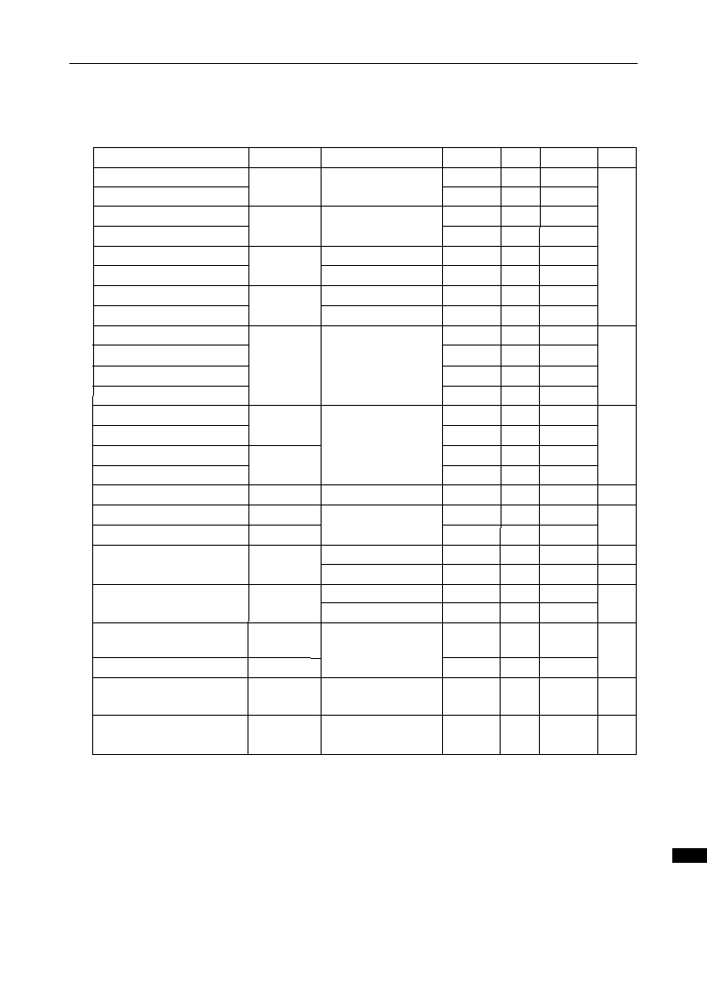
25-3
MSM66591/ML66592 User's Manual
Chapter 25 Electrical Characteristics
25
25.3 DC Characteristics
MSM66591
1. Applied to P0
2. Applied to P1≠P12 (excluding P7_0≠P7_3)
3. Applied to AI0≠AI23
4. Applied to P7_0≠P7_3
5. Applied to
RES
6. Applied to
EA
,
OE
, NMI
7. Applied to OSC0
* Ports configured to be input should be connected to V
DD
or 0 V; other ports should
take no load.
Parameter
Symbol
Condition
Min.
Typ.
Max.
Unit
"H" level input voltage
2.2
--
V
DD
+ 0.3
1
"H" level input voltage
V
IH
--
0.80V
DD
--
V
DD
+ 0.3
2,4,5,6,7
"L" level input voltage
≠0.3
--
0.8
1
"L" level input voltage
V
IL
--
≠0.3
--
0.2V
DD
V
2,4,5,6,7
"H" level output voltage
V
OH
I
O
= ≠400 mA
V
DD
≠ 0.4
--
--
1,4
"H" level output voltage
I
O
= ≠200 mA
V
DD
≠ 0.4
--
--
2
"L" level output voltage
V
OL
I
O
= 3.2 mA
--
--
0.4
1,4
"L" level output voltage
I
O
= 1.6 mA
--
--
0.4
2
Input leakage current
Input leakage current
I
IH
/I
IL
--
--
1/≠1
6
--
--
0.1/≠0.1
3
Input current
V
I
= V
DD
/0 V
--
--
1/≠250
µ
A
5
Input current
--
--
15/≠15
7
"H" level output current
I
OH
V
O
= 2.4 V
≠2
--
--
mA
1,4
"H" level output current
≠1
--
--
2
"L" level output current
I
OL
10
--
--
1,4
"L" level output current
5
--
--
2
Output leakage current
I
LO
V
O
= V
DD
/0 V
--
--
±
2
µ
A
1,2,4
Input capacity
C
I
f = 1 MHz, Ta = 25
∞
C
--
5
--
pF
Output capacity
C
O
--
7
--
Analog reference power
supply current
I
REF
A/D conversion in progress
--
--
12
12
1
mA
V
mA
Supply current
(in STOP mode)
I
DDS
V
DD
= 2 V, Ta = 25
∞
C *
V
DD
= 4.75 to 5.25 V V
DD
+ 4.75
V
DD
= 4.75 to 5.25 V
V
IHV
= V
DD
+ 0.3 to 12 V
--
0.2
10
µ
A
Supply current
(in HALT mode)
High-voltage tolerant
input voltage
*3,4
High-voltage tolerant
input current
*3,4
I
DDH
V
IHV
I
IHV
f
OSC
= 24 MHz
*1
,
No Load
--
mA
Supply current
I
DD
--
--
A/D conversion stopped
--
--
--
--
10
µ
A
--
1
100
*
(V
DD
= 5 V
±
10%, Ta = ≠40 to +115
∞
C)
*2
55
80
70
100

25-4
MSM66591/ML66592 User's Manual
Chapter 25 Electrical Characteristics
*1 f
OSC
is the frequency of the internal master clock.
*2 If this device is used in circumstances where the ambient temperature (Ta) exceeds
85
∞
C, be sure to contact your local Oki sales office in advance.
*3 Applied to TEST,
EA
. Only for MSM66Q591
*4 When programming data into Flash ROM using Oki's Flash ROM programmer or
YDC's Flash ROM programmer, use a resistor of 1 k
or less if connecting an
external resistor in series with the TEST pin.
Apply a high voltage to the TEST or
EA
pin after a voltage within the range (4.75 to
5.25 V) guaranteed for operation is applied to V
DD
.
Remove a high voltage from the TEST or
EA
pin while a voltage within the range
(4.75 to 5.25 V) guaranteed for operation is being applied to V
DD
.
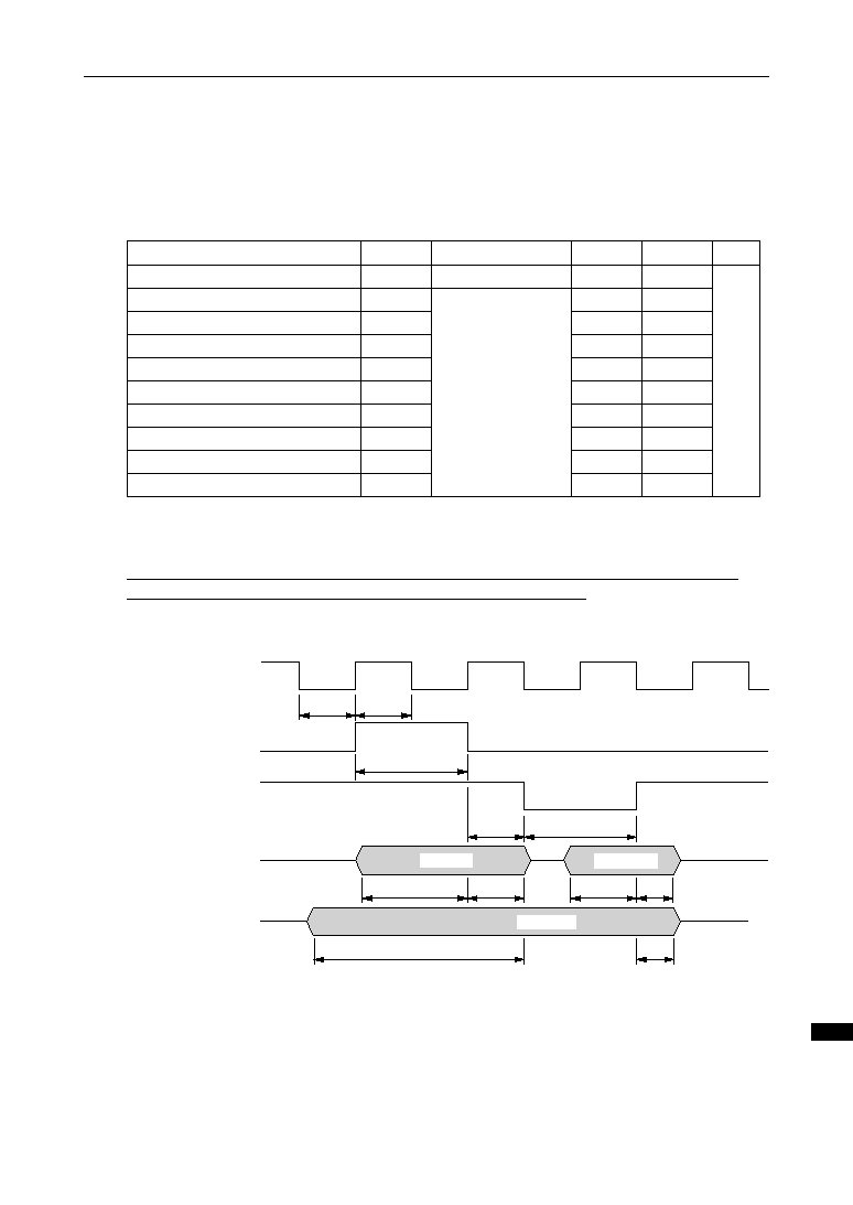
25-5
MSM66591/ML66592 User's Manual
Chapter 25 Electrical Characteristics
25
Parameter
Symbol
Condition
Min.
Max.
Unit
Master clock (CLK) pulse width
t
¯W
*1
--
20.8
25
ns
ALE pulse width
t
AW
2t
¯W
≠ 10
--
PSEN pulse width
t
PW
2t
¯W
≠ 10
--
PSEN pulse delay time
t
PAD
t
¯W
≠ 10
t
¯W
+ 10
Low address setup time
t
ALS
2t
¯W
≠ 15 2t
¯W
+ 3
Low address hold time
t
ALH
C
L
= 50 pF
t
¯W
≠ 10
t
¯W
+ 10
High address setup time
t
AHS
3t
¯W
≠ 10 4t
¯W
+ 3
High address hold time
t
APH
0
t
¯W
+ 10
Instruction setup time
t
IS
--
Instruction hold time
t
IH
0
t
¯W
≠ 10
(V
DD
= 5 V
±
10%, Ta = ≠40 to +115
∞
C)
*2
30
*1
The master clock pulse is the frequency generated by multiplying the original oscillation
clock by 2.
*2
If this device is used in circumstances where the ambient temperature (Ta) exceeds
85
∞
C, be sure to contact your local Oki sales office in advance.
Master clock (CLK)
(internal)
ALE
t¯
W
t¯
W
PSEN
t
AW
t
PAD
t
PW
AD0≠AD7
t
ALS
t
ALH
t
IS
t
IH
A8≠A16
t
AHS
t
APH
PC0≠7
PC8≠16
INST0≠7
25.4 AC Characteristics
[1]
External Program Memory Control
MSM66591
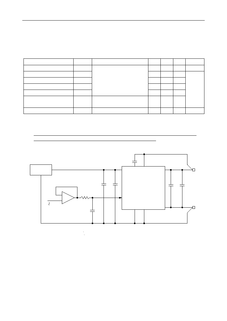
25-6
MSM66591/ML66592 User's Manual
Chapter 25 Electrical Characteristics
25.5 A/D Converter Characteristics
MSM66591
Reference
Voltage
≠
+
Analog input
C
I
0.1
µ
F
47
µ
F
+
V
REF
AI0≠AI23
0.1
µ
F
AGND
GND
AV
DD
V
DD
0.1
µ
F
47
µ
F
+
+5 V
0 V
R
I
(Analog input source impedance) £ 5 kW
C
I
= 0.1
µ
F
R
I
MSM66591
Figure 25-1 Measurement Circuit (MSM66591)
Parameter
Symbol
Condition
Min.
Typ.
Max.
Unit
n
Refer to the measurement
circuit (Figure 25-1)
Analog input source impedance
--
--
10
Bit
Resolution
E
L
--
--
Linearity error
E
D
--
--
--
Differential linearity error
E
ZS
--
LSB
Zero scale error
E
FS
--
--
Full scale error
E
CT
Refer to the measurement
circuit (Figure 25-2)
--
--
Crosstalk
t
CONV
by ADTM set data
10.7
--
21.3
µ
s/ch
Conversion time
(Ta = ≠40 to +115
∞
C, AV
DD
= V
DD
= V
REF
= 5 V
±
10%, AGND = GND = 0 V, f
OSC
= 24 MHz)
*1,2
R
I
£ 5 kW
t
CONV
= 16
µ
s
±
3
±
1
+3
≠3
±
1
*1
f
OSC
is the frequency of the internal master clock (the master clock is the frequency
generated by multiplying the original oscillation clock by 2).
*2
If this device is used in circumstances where the ambient temperature (Ta) exceeds
85
∞
C, be sure to contact your local Oki sales office in advance.

25-7
MSM66591/ML66592 User's Manual
Chapter 25 Electrical Characteristics
25
Figure 25-2 Crosstalk Measurement Circuit (MSM66591)
Definition of Terminology
1.
Resolution
Resolution is the value of minimum discernible analog input.
With 10 bits, since 2
10
= 1024, resolution of (V
REF
≠ AGND)
˜
1024 is possible.
2.
Linearity error
Linearity error is the difference between ideal conversion characteristics and actual
conversion characteristics of a 10-bit A/D converter (not including quantization error).
Ideal conversion characteristics can be obtained by dividing the voltage between V
REF
and AGND into 1024 equal steps.
3.
Differential linearity error
Differential linearity error indicates the smoothness of conversion characteristics.
Ideally, the range of analog input voltage that corresponds to 1 converted bit of digital
output is 1LSB = (V
REF
≠ AGND)
˜
1024. Differential error is the difference between
this ideal bit size and bit size of an arbitrary point in the conversion range.
4.
Zero scale error
Zero scale error is the difference between ideal conversion characteristics and actual
conversion characteristics at the point where the digital output changes from 000H to
001H.
5.
Full-scale error
Full-scale error is the difference between ideal conversion characteristics and actual
conversion characteristics at the point where the digital output changes from 3FEH to
3FFH.
≠
+
Analog input
0.1
µ
F
AI0
5 kW
AI1
AI23
V
REF
or AGND
Crosstalk is defined as the
difference between the A/D
conversion result when applying
the identical analog
input to AI0≠AI23 and the A/D
conversion result in the circuit
in the left figure.
MSM66591
25-8
MSM66591/ML66592 User's Manual
Chapter 25 Electrical Characteristics
Parameter
GND = AGND = 0 V
Ta = 25
∞
C
Rating
≠0.3 to +7.0
≠0.3 to V
DD
+ 0.3
≠0.3 to V
DD
+ 0.3
≠0.3 to V
DD
+ 0.3
≠0.3 to V
REF
730
50
≠50 to +150
Unit
V
Symbol
V
DD
V
I
V
O
AV
DD
P
D
V
AI
T
STG
--
per output
per package
Condition
Ta = 95
∞
C
*1
Digital power supply voltage
Input voltage
Output voltage
Analog power supply voltage
mW
∞
C
Power dissipation
Storage temperature
High-voltage tolerant
input voltage
*2
Analog reference voltage
Analog input voltage
V
REF
V
HV
≠0.3 to V
DD
+ 0.3 and
≠0.3 to AV
DD
+ 0.3
≠0.3 to +13
[ML66592 Electrical Characteristics]
25.6 Absolute Maximum Ratings
ML66592
*1
If this device is used in circumstances where the ambient temperature (Ta) exceeds
85
∞
C, be sure to contact your local Oki sales office in advance.
*2
Applied to TEST,
EA
. Only for ML66Q592
Apply a high voltage to the TEST or
EA
pin after a voltage within the range (4.75 to 5.25
V) guaranteed for operation is applied to V
DD
.
Remove a high voltage from the TEST or
EA
pin while a voltage within the range (4.75
to 5.25 V) guaranteed for operation is being applied to V
DD
.

25-9
MSM66591/ML66592 User's Manual
Chapter 25 Electrical Characteristics
25
Parameter
Range
4.5 to 5.5
4.5 to 5.5
AV
DD
≠ 0.3 to AV
DD
AGND to V
REF
2.0 to 5.5
20 to 28
≠40 to +95
20
2
1
Unit
V
Symbol
V
DD
AV
DD
V
REF
V
AI
V
DDH
N
f
OSC
*1
Ta
*2
--
V
DD
= 5 V
±
10%
P1≠P12 (except
P7_0≠P7_3)
P0, P7_0≠P7_3
MOS load
Condition
TTL load
Digital power supply voltage
Analog power supply voltage
Analog reference voltage
Analog input voltage
Memory hold voltage
Operating frequency
Ambient temperature
Fanout
MHz
f
OSC
= 0 Hz
*1
--
--
V
DD
= A
VDD
20 MHz
£ f
OSC
£ 28 MHz
*1
--
--
--
Flash ROM programming
cycle
*3
Ambient temperature
during Flash ROM
programming
*3
Digital power supply
voltage during Flash ROM
programming
*3
V
WR
T
WR
C
WR
V
DD
= 4.75 to 5.25 V
Ta = ≠40 to +90
∞
C
Ta = ≠40 to +90
∞
C
V
DD
= 4.75 to 5.25 V
4.75 to 5.25
≠40 to +90
100
cycle
V
∞
C
∞
C
25.7 Operating Range
ML66592
*1
f
OSC
is the frequency of the internal master clock (the master clock is the frequency
generated by multiplying the original oscillation clock by 2).
*2
If this device is used in circumstances where the ambient temperature (Ta) exceeds
85
∞
C, be sure to contact your local Oki sales office in advance.
*3
Only for ML66Q592

25-10
MSM66591/ML66592 User's Manual
Chapter 25 Electrical Characteristics
25.8 DC Characteristics
ML66592
1. Applied to P0
2. Applied to P1≠P12 (excluding P7_0≠P7_3)
3. Applied to AI0≠AI23
4. Applied to P7_0≠P7_3
5. Applied to
RES
6. Applied to
EA
,
OE
, NMI
7. Applied to OSC0
* Ports configured to be input should be connected to V
DD
or 0 V; other ports should
take no load.
Parameter
Symbol
Condition
Min.
Typ.
Max.
Unit
"H" level input voltage
2.2
--
V
DD
+ 0.3
1
"H" level input voltage
V
IH
--
0.80V
DD
--
V
DD
+ 0.3
2,4,5,6,7
"L" level input voltage
≠0.3
--
0.8
1
"L" level input voltage
V
IL
--
≠0.3
--
0.2V
DD
V
2,4,5,6,7
"H" level output voltage
V
OH
I
O
= ≠400 mA
V
DD
≠ 0.4
--
--
1,4
"H" level output voltage
I
O
= ≠200 mA
V
DD
≠ 0.4
--
--
2
"L" level output voltage
V
OL
I
O
= 3.2 mA
--
--
0.4
1,4
"L" level output voltage
I
O
= 1.6 mA
--
--
0.4
2
Input leakage current
Input leakage current
I
IH
/I
IL
--
--
1/≠1
6
--
--
0.1/≠0.1
3
Input current
V
I
= V
DD
/0 V
--
--
1/≠250
µ
A
5
Input current
--
--
15/≠15
7
"H" level output current
I
OH
V
O
= 2.4 V
≠2
--
--
mA
1,4
"H" level output current
≠1
--
--
2
"L" level output current
I
OL
10
--
--
1,4
"L" level output current
5
--
--
2
Output leakage current
I
LO
V
O
= V
DD
/0 V
--
--
±
2
µ
A
1,2,4
Input capacity
C
I
f = 1 MHz, Ta = 25
∞
C
--
5
--
pF
Output capacity
C
O
--
7
--
Analog reference power
supply current
I
REF
A/D conversion in progress
--
--
12
12
1
mA
V
mA
Supply current
(in STOP mode)
I
DDS
V
DD
= 2 V, Ta = 25
∞
C *
V
DD
= 4.75 to 5.25 V V
DD
+ 4.75
V
DD
= 4.75 to 5.25 V
V
IHV
= V
DD
+ 0.3 to 12 V
--
0.2
10
µ
A
Supply current
(in HALT mode)
High-voltage tolerant
input voltage
*3,4
High-voltage tolerant
input current
*3,4
I
DDH
V
IHV
I
IHV
f
OSC
= 28 MHz
*1
,
No Load
--
mA
Supply current
I
DD
--
--
A/D conversion stopped
--
--
--
--
10
µ
A
--
1
100
*
(V
DD
= 5 V
±
10%, Ta = ≠40 to +95
∞
C)
*2
65
95
90
120

25-11
MSM66591/ML66592 User's Manual
Chapter 25 Electrical Characteristics
25
*1 f
OSC
is the frequency of the internal master clock.
*2 If this device is used in circumstances where the ambient temperature (Ta) exceeds
85
∞
C, be sure to contact your local Oki sales office in advance.
*3 Applied to TEST,
EA
. Only for ML66Q592
*4 When programming data into Flash ROM using Oki's Flash ROM programmer or
YDC's Flash ROM programmer, use a resistor of 1 k
or less if connecting an
external resistor in series with the TEST pin.
Apply a high voltage to the TEST or
EA
pin after a voltage within the range (4.75 to
5.25 V) guaranteed for operation is applied to V
DD
.
Remove a high voltage from the TEST or
EA
pin while a voltage within the range
(4.75 to 5.25 V) guaranteed for operation is being applied to V
DD
.
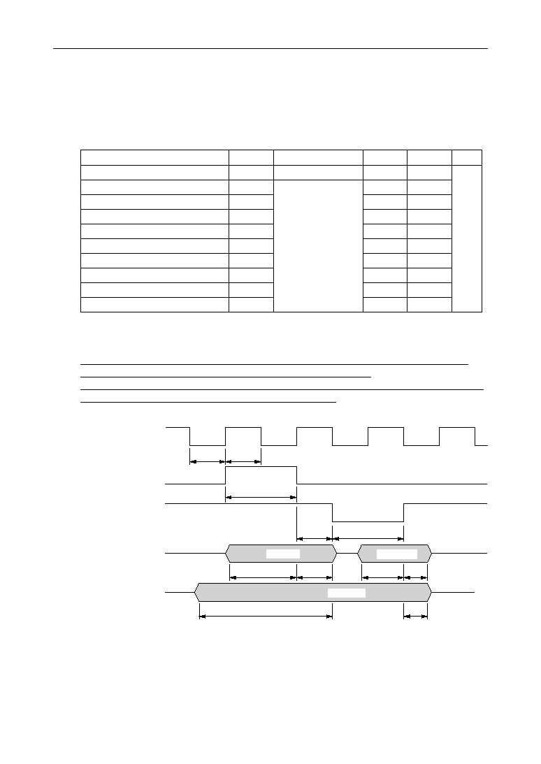
25-12
MSM66591/ML66592 User's Manual
Chapter 25 Electrical Characteristics
Parameter
Symbol
Condition
Min.
Max.
Unit
Master clock (CLK) pulse width
t
¯W
*1
--
20.8
25
ns
ALE pulse width
t
AW
2t
¯W
≠ 10
--
PSEN pulse width
t
PW
2t
¯W
≠ 10
--
PSEN pulse delay time
t
PAD
t
¯W
≠ 10
t
¯W
+ 10
Low address setup time
t
ALS
2t
¯W
≠ 15 2t
¯W
+ 3
Low address hold time
t
ALH
f
OSC
24 MHz
*3
C
L
= 50 pF
t
¯W
≠ 10
t
¯W
+ 10
High address setup time
t
AHS
3t
¯W
≠ 10 4t
¯W
+ 3
High address hold time
t
APH
0
t
¯W
+ 10
Instruction setup time
t
IS
--
Instruction hold time
t
IH
0
t
¯W
≠ 10
(V
DD
= 5 V
±
10%, Ta = ≠40 to +95
∞
C)
*2
30
*1
The master clock pulse is the frequency generated by multiplying the original oscillation
clock by 2.
*2
If this device is used in circumstances where the ambient temperature (Ta) exceeds
85
∞
C, be sure to contact your local Oki sales office in advance.
*3
In the ML66Q592, the electrical characteristics for external memory access apply when
the (internal) master clock frequency is 24 MHz or less.
Master clock (CLK)
(internal)
ALE
t¯
W
t¯
W
PSEN
t
AW
t
PAD
t
PW
AD0≠AD7
t
ALS
t
ALH
t
IS
t
IH
A8≠A17
t
AHS
t
APH
PC0≠7
PC8≠17
INST0≠7
25.9 AC Characteristics (Preliminary)
[1]
External Program Memory Control
ML66592
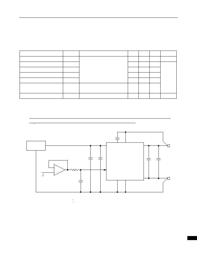
25-13
MSM66591/ML66592 User's Manual
Chapter 25 Electrical Characteristics
25
25.10 A/D Converter Characteristics
ML66592
Reference
Voltage
≠
+
Analog input
C
I
0.1
µ
F
47
µ
F
+
V
REF
AI0≠AI23
0.1
µ
F
AGND
GND
AV
DD
V
DD
0.1
µ
F
47
µ
F
+
+5 V
0 V
R
I
(Analog input source impedance) £ 5 kW
C
I
= 0.1
µ
F
R
I
ML66592
Figure 25-3 Measurement Circuit (ML66592)
Parameter
Symbol
Condition
Min.
Typ.
Max.
Unit
n
Refer to the measurement
circuit (Figure 25-3)
Analog input source impedance
--
--
10
Bit
Resolution
E
L
--
--
Linearity error
E
D
--
--
--
Differential linearity error
E
ZS
--
LSB
Zero scale error
E
FS
--
--
Full scale error
E
CT
Refer to the measurement
circuit (Figure 25-4)
--
--
Crosstalk
t
CONV
by ADTM set data
9.1
--
18.3
µ
s/ch
Conversion time
(Ta = ≠40 to +95
∞
C, AV
DD
= V
DD
= V
REF
= 5 V
±
10%, AGND = GND = 0 V, f
OSC
= 28 MHz)
*1,2
R
I
£ 5 kW
t
CONV
= 18.3
µ
s
±
3
±
1
+3
≠3
±
1
*1
f
OSC
is the frequency of the internal master clock (the master clock is the frequency
generated by multiplying the original oscillation clock by 2).
*2
If this device is used in circumstances where the ambient temperature (Ta) exceeds
85
∞
C, be sure to contact your local Oki sales office in advance.
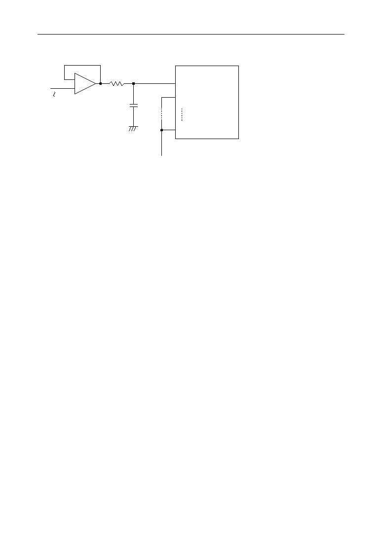
25-14
MSM66591/ML66592 User's Manual
Chapter 25 Electrical Characteristics
Figure 25-4 Crosstalk Measurement Circuit (ML66592)
Definition of Terminology
1.
Resolution
Resolution is the value of minimum discernible analog input.
With 10 bits, since 2
10
= 1024, resolution of (V
REF
≠ AGND)
˜
1024 is possible.
2.
Linearity error
Linearity error is the difference between ideal conversion characteristics and actual
conversion characteristics of a 10-bit A/D converter (not including quantization error).
Ideal conversion characteristics can be obtained by dividing the voltage between V
REF
and AGND into 1024 equal steps.
3.
Differential linearity error
Differential linearity error indicates the smoothness of conversion characteristics.
Ideally, the range of analog input voltage that corresponds to 1 converted bit of digital
output is 1LSB = (V
REF
≠ AGND)
˜
1024. Differential error is the difference between
this ideal bit size and bit size of an arbitrary point in the conversion range.
4.
Zero scale error
Zero scale error is the difference between ideal conversion characteristics and actual
conversion characteristics at the point where the digital output changes from 000H to
001H.
5.
Full-scale error
Full-scale error is the difference between ideal conversion characteristics and actual
conversion characteristics at the point where the digital output changes from 3FEH to
3FFH.
≠
+
Analog input
0.1
µ
F
AI0
5 kW
AI1
AI23
V
REF
or AGND
Crosstalk is defined as the
difference between the A/D
conversion result when applying
the identical analog
input to AI0≠AI23 and the A/D
conversion result in the circuit
in the left figure.
ML66592

Package Dimensions
Chapter 26
26

26-1
MSM66591/ML66592 User's Manual
Chapter 26 Package Dimensions
26
Notes for Mounting the Surface Mount Type Package
The surface mount type packages are very susceptible to heat in reflow mounting and
humidity absorbed in storage.
Therefore, before you perform reflow mounting, contact Oki's responsible sales person for
the product name, package name, pin number, package code and desired mounting
conditions (reflow method, temperature and times).
26. Package Dimensions
LQFP144-P-2020-0.50-K
Package material
Lead frame material
Pin treatment
Rev. No./Last Revised
Epoxy resin
42 alloy
Solder plating (
5 mm)
5/Nov. 28, 1996
Package weight (g)
1.37 TYP.
(Unit : mm)
Oki Electric Industry Co., Ltd.
Mirror finish

26-2
MSM66591/ML66592 User's Manual
Chapter 26 Package Dimensions

Revision History
Chapter 27
27

27-1
MSM66591/ML66592 User's Manual
Chapter 27 Revision History
27
27. Revision History
Document
No.
Date
Page
--
--
Description
FEUL66591-66592-01
First edition
Mar. 4, 2002
Previous
Edition
Current
Edition

27-2
MSM66591/ML66592 User's Manual
Chapter 27 Revision History

NOTICE
1.
The information contained herein can change without notice owing to product and/or
technical improvements. Before using the product, please make sure that the information
being referred to is up-to-date.
2.
The outline of action and examples for application circuits described herein have been
chosen as an explanation for the standard action and performance of the product. When
planning to use the product, please ensure that the external conditions are reflected in the
actual circuit, assembly, and program designs.
3.
When designing your product, please use our product below the specified maximum
ratings and within the specified operating ranges including, but not limited to, operating
voltage, power dissipation, and operating temperature.
4.
Oki assumes no responsibility or liability whatsoever for any failure or unusual or
unexpected operation resulting from misuse, neglect, improper installation, repair, alteration
or accident, improper handling, or unusual physical or electrical stress including, but not
limited to, exposure to parameters beyond the specified maximum ratings or operation
outside the specified operating range.
5.
Neither indemnity against nor license of a third party's industrial and intellectual property
right, etc. is granted by us in connection with the use of the product and/or the information
and drawings contained herein. No responsibility is assumed by us for any infringement
of a third party's right which may result from the use thereof.
6.
The products listed in this document are intended for use in general electronics equipment
for commercial applications (e.g., office automation, communication equipment,
measurement equipment, consumer electronics, etc.). These products are not authorized
for use in any system or application that requires special or enhanced quality and reliability
characteristics nor in any system or application where the failure of such system or
application may result in the loss or damage of property, or death or injury to humans.
Such applications include, but are not limited to, traffic and automotive equipment, safety
devices, aerospace equipment, nuclear power control, medical equipment, and life-support
systems.
7.
Certain products in this document may need government approval before they can be
exported to particular countries. The purchaser assumes the responsibility of determining
the legality of export of these products and will take appropriate and necessary steps at their
own expense for these.
8.
No part of the contents contained herein may be reprinted or reproduced without our prior
permission.
Copyright 2002 Oki Electric Industry Co., Ltd.
Printed in Japan


