
1/30
° Semiconductor
MSM6665-xx
° Semiconductor
MSM6665-xx
DOT MATRIX LCD CONTROLLER WITH 17-DOT COMMON DRIVER AND 80-DOT SEGMENT
DRIVER
GENERAL DESCRIPTION
The MSM6665-xx is a dot-matrix LCD control driver which has functions of displaying charac-
ters, cursor and arbitrators.
The MSM6665-xx is provided with a 17-dot common driver, 80-dot segment driver, display RAM
and character ROM, and is controlled with the commands from the serial interface.
The character ROM can change the font data by mask option.
The MSM6665-01 has standard ROM with 256 different character fonts.
The MSM6665-xx can drive a variety of LCD panels because of the bias voltage, which determines
the LCD driving voltage, can be optionally supplied from the external source.
FEATURES
∑ Logic supply voltage
: 2.5 to 5.5 V
∑ LCD driving voltage
: 3.0 to 6.0 V
∑ Serial interface
∑ Contains a 17-dot common driver and an 80-dot segment driver
∑ Contains ROM with character fonts of (5 x 7 dot) x 256
∑ Built-in RC oscillator circuit
∑ Provided with 80-dot arbitrators
∑ Switchable between 1/9 duty (1 line; characters + cursor + arbitrator) and 1/17 duty (2 lines;
characters + cursor, 1 line; arbitrator)
∑ Character blink operation can be switched between all-characters lighting-on mode and all-
characters lighting-off mode
∑ Arbitrator blink operation can be switched between 5-dot unit mode and 1-dot unit mode
∑ Package options:
128-pin plastic QFP (QFP128-P-1420-0.50-K) (Product name: MSM6665-01GS-K)
Al pad chip
(Product name: MSM6665-xx)
xx indicates code number.
E2B0036-27-Y2
This version: Nov. 1997
Previous version: Mar. 1996
2/30
° Semiconductor
MSM6665-xx
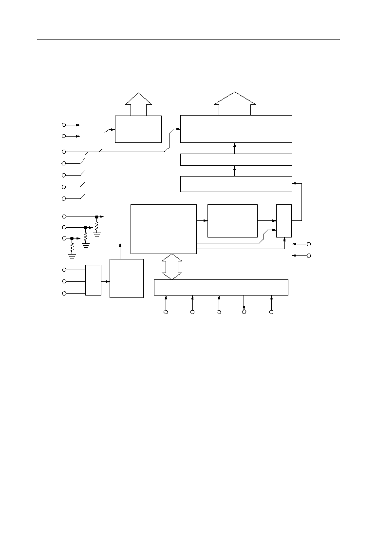
FREQUENCY
DIVIDER
&
TIMING
GENERATION
V
DD
V
SS
V
SS1
V
SS2
V
SS3
V
SS4
V
SS5
TEST1
TEST2
TEST3
OSC1
OSC2
OSC3
S E R I A L / P A R A L L E L I N T E R F A C E
C S
C /
SHT
S O
S I
D
8
R A M
( 5 1 2 - b i t )
S 1 - S 8 0
80
SEGMENT
DRIVER
LATCH
SHIFT REGISTER
COMMON
DRIVER
17
9D/
RST
OSC
CHARACTER
GENERATOR
ROM
(256x5x7dot)
F/F
GATE
C 1 - C 1 7
17D
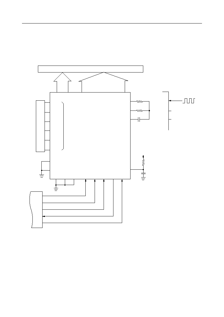
BLOCK DIAGRAM
3/30
° Semiconductor
MSM6665-xx
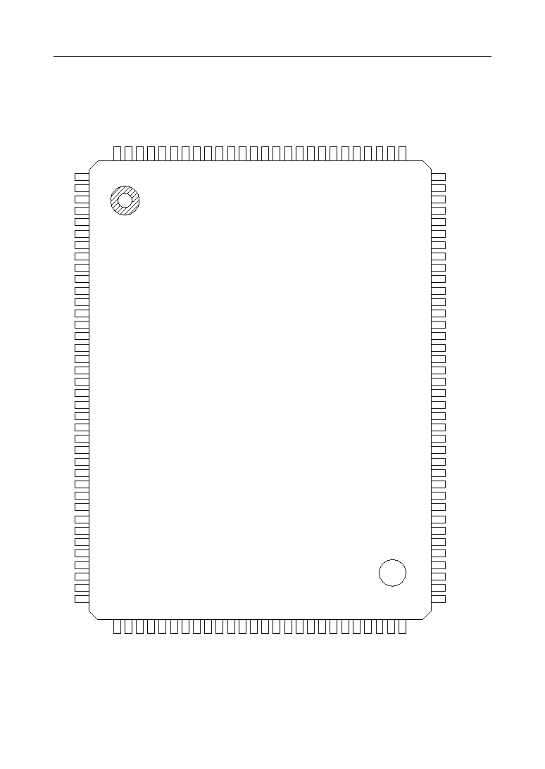
PIN CONFIGURATION (TOP VIEW)
NC : No connection
128-Pin Plastic QFP
58
1
2
3
4
5
6
7
8
9
10
11
12
13
14
15
16
17
18
19
20
21
22
23
24
25
26
27
28
29
30
S57
S56
S55
S54
S53
S52
S51
S50
S49
S48
S47
S46
NC
S45
S44
NC
S43
S42
S41
S40
S39
S38
NC
S37
S36
NC
S35
S34
S33
S32
57
56
55
54
53
52
51
50
49
48
47
46
45
44
43
42
41
40
39
S4
S5
S6
S7
S8
S9
S10
S11
S12
S13
S14
S15
S16
S17
S18
S19
S20
S21
S22
S23
102
101
100
99
98
97
96
95
94
93
92
91
90
89
88
87
86
85
84
83
82
81
80
79
78
77
76
75
74
73
TEST1
OSC3
OSC2
NC
OSC1
V
DD
SO
RST
9D/17D
SHT
SI
C/D
NC
CS
V
SS1
NC
V
SS2
V
SS3
V
SS4
V
SS5
V
SS
(GND)
C1
NC
C2
C3
NC
C4
C5
C6
C7
S77
S76
S75
S74
S73
S72
S71
S70
S69
S68
S67
S66
S65
S64
S63
S62
S61
S60
S59
S58
109
110
111
112
113
114
115
116
117
118
119
120
121
122
123
124
125
126
127
128
31
32
33
34
35
36
37
38
S31
S30
S29
S28
S27
S26
S25
S24
72
71
70
69
68
67
66
65
C8
C9
C10
C11
C12
C13
C14
C15
64
63
62
61
60
49
NC
C16
C17
S1
S2
S3
TEST2
TEST3
NC
S80
S79
S78
103
104
105
106
107
108

4/30
° Semiconductor
MSM6665-xx
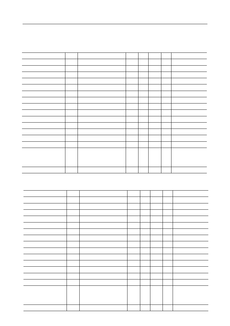
ABSOLUTE MAXIMUM RATINGS
*1:
The power dissipation depends on the heat sink characteristic of the package.
Set a junction temperature at 150
∞
C or lower.
RECOMMENDED OPERATING CONDITIONS
*2:
RC oscillation, external input clock frequency
List of bias voltages
Symbol
V
DD
V
SS1
V
SS2
V
SS3
V
SS4
V
SS5
1/5 bias
V
DD
V
DD
≠1/5V
BI
V
DD
≠2/5V
BI
V
DD
≠3/5V
BI
V
DD
≠4/5V
BI
V
SS5
Remarks
Highest voltage
Lowest voltage
1/4 bias
V
DD
V
DD
≠1/4V
BI
V
DD
≠2/4V
BI
V
DD
≠3/4V
BI
V
SS5
(V
BI
=V
DD
≠V
SS5
)
--
--
--
--
Parameter
Unit
Condition
Supply Voltage
Input Voltage
Power Dissipation
Symbol
Storage Temperature
Rating
Applicable pin
≠0.3 to +7
≠0.3 to V
DD
+0.3
630
≠55 to +150
V
V
mW
∞C
V
DD
, V
SS
All inputs
Bias Voltage
Ta=25∞C, V
DD
≠V
SS5
≠0.3 to +7
V
V
DD
, V
SS5
Ta=85∞C
QFP128-1420
*1
V
DD
V
BI
V
I
P
D
T
STG
Ta=25∞C, V
DD
≠V
SS
--
--
--
--
Parameter
Unit
Condition
Supply Voltage
Operating Frequency
Symbol
Operating Temperature
Rating
Applicable pin
2.5 to 5.5
65 to 115
≠40 to +85
V
kHz
∞C
V
DD
, V
SS
OSC1
Bias Voltage
V
DD
≠V
SS5
3 to 6
V
V
DD
, V
SS5
V
DD
V
BI
f
op
T
op
V
DD
≠V
SS
*2
--
--
5/30
° Semiconductor
MSM6665-xx
ELECTRICAL CHARACTERISTICS
DC Characteristics (1)
DC Characteristics (2)
Parameter
--
--
(V
DD
=2.5 to 3.5V, V
BI
=3 to 6V, Ta=≠40 to +85∞C)
"H" Input Voltage 1
V
IH1
"L" Input Voltage 1
V
IL1
"H" Input Voltage 2
V
IH2
"L" Input Voltage 2
V
IL2
"H" Input Current 1
I
IH1
"L" Input Current
I
IL
"H" Input Current 2
I
IH2
"H" Output Voltage
V
OH
"L" Output Voltage
V
OL
OFF Leakage
I
OFF
OSC "H" Output Current
I
OH
OSC "L" Output Current
I
OL
COM Output Resistance
R
C
SEG Output Resistance
R
S
Supply Current 1
I
DD1
Supply Current 2
I
DD2
External clock input
External clock input
V
I
=V
DD
V
I
=0V
Pull-down resistance, V
I
=V
DD
I
O
=≠1.5mA
I
O
=500mA
V
I
=V
DD
/0V
V
I
=V
DD
≠0.5V
V
I
=0.5V
I
O
=±50mA
I
O
=±10mA
RC oscillation, f=80kHz
C=56pF, R
S
=10kW
R=76kW, no load
External clock, f=80kHz
Symbol
Condition
Min. Typ. Max. Unit
Applicable pin
0.8V
DD
--
V
DD
V
OSC1
0
-- 0.2V
DD
V
OSC1
0.8V
DD
--
V
DD
V
Input pins except OSC1
0
-- 0.2V
DD
V
Input pins except OSC1
--
--
1
m
A
Input pins except TEST
--
--
≠1
m
A
Input pins
0.05
--
0.4
mA TEST1-TEST3
V
DD
≠0.5
--
--
V
S0
--
--
0.5
V
S0
--
--
±1
m
A
S0
--
--
≠0.25 mA OSC2, OSC3
0.25
--
--
mA OSC2, OSC3
--
--
6
kW C1-C17
--
--
15
kW S1-S80
--
--
0.5
mA
--
--
--
100
m
A
--
.
.
Parameter
--
--
(V
DD
=4.5 to 5.5V, V
BI
=3 to 6V, Ta=≠40 to +85∞C)
"H" Input Voltage 1
V
IH1
"L" Input Voltage 1
V
IL1
"H" Input Voltage 2
V
IH2
"L" Input Voltage 2
V
IL2
"H" Input Current 1
I
IH1
"L" Input Current
I
IL
"H" Input Current 2
I
IH2
"H" Output Voltage
V
OH
"L" Output Voltage
V
OL
OFF Leakage
I
OFF
OSC "H" Output Current
I
OH
OSC "L" Output Current
I
OL
COM Output Resistance
R
C
SEG Output Resistance
R
S
Supply Current 1
I
DD1
Supply Current 2
I
DD2
External clock input
External clock input
V
I
=V
DD
V
I
=0V
Pull-down resistance, V
I
=V
DD
I
O
=≠1.5mA
I
O
=500mA
V
I
=V
DD
/0V
V
I
=V
DD
≠0.5V
V
I
=0.5V
I
O
=±50mA
I
O
=±10mA
RC oscillation, f=80kHz
C=56pF, R
S
=10kW
R=76kW, no load
External clock, f=80kHz
Symbol
Condition
Min. Typ. Max. Unit
Applicable pin
0.8V
DD
--
V
DD
V
OSC1
0
-- 0.2V
DD
V
OSC1
0.8V
DD
--
V
DD
V
Input pins except OSC1
0
-- 0.2V
DD
V
Input pins except OSC1
--
--
1
m
A
Input pins except TEST
--
--
≠1
m
A
Input pins
0.3
--
1.4
mA TEST1-TEST3
V
DD
≠0.5
--
--
V
S0
--
--
0.5
V
S0
--
--
±1
m
A
S0
--
--
≠0.5
mA OSC2, OSC3
0.5
--
--
mA OSC2, OSC3
--
--
6
kW C1-C17
--
--
15
kW S1-S80
--
--
1.1
mA
--
--
--
400
m
A
--
.
.
6/30
° Semiconductor
MSM6665-xx
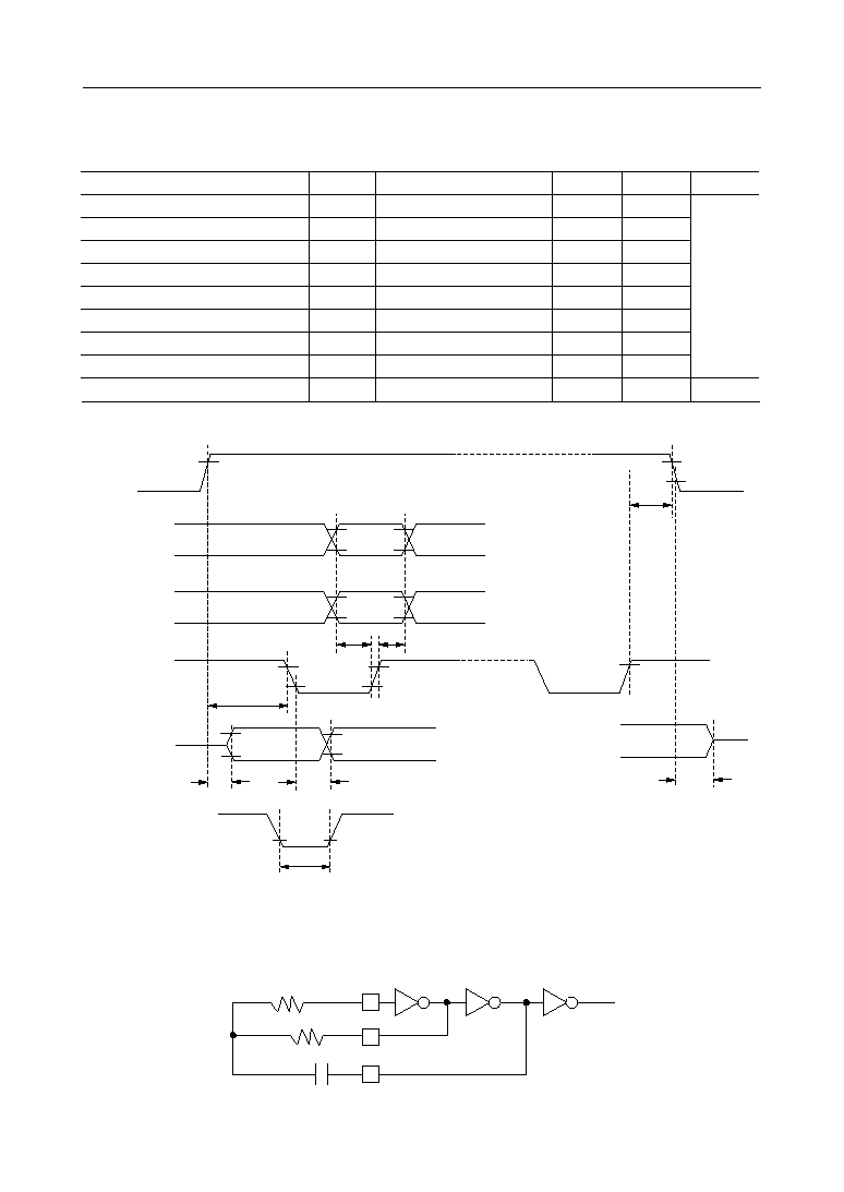
AC Characteristics
Parameter
Min.
Unit
Symbol
Condition
Max.
300
200
0
200
200
5
200
50
ns
µs
200
200
--
--
--
--
--
--
--
--
(V
DD
≠V
SS
=2.5 to 5.5V, Ta=≠40 to +85∞C)
CS Setup Time
t
CS
--
CS Hold Time
t
CH
--
SO ON Delay Time
t
ON
--
SO OFF Delay Time
t
OFF
--
SO Output Delay Time
t
DLY
Input Setup Time
t
IS
--
Input Hold Time
t
IH
--
Input Waveform Rise Time, Fall Time
t
r,
t
f
Reset Pulse Input Pulse Width
t
RT
--
C
L
=45pF
All inputs
t
IS
C S
S I
C /
SHT
S O
RST
D
t
IH
t
CS
"Z"
t
ON
t
DLY
t
RT
t
OFF
"Z"
t
CH
V
IH2
V
IL2
V
IL2
V
IH2
V
IL2
V
IH2
V
IL2
V
IH2
V
IL2
V
OH
V
OL
V
IH2
=0.8V
DD
V
IL2
=0.2V
DD
V
OH
=V
DD
≠0.5V
V
OL
=0.5V
*
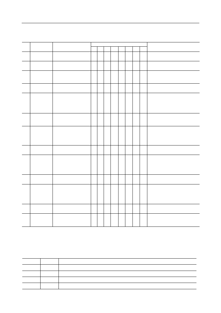
Oscillation Circuit
R
S
C OSC3
R
OSC2
OSC1
7/30
° Semiconductor
MSM6665-xx
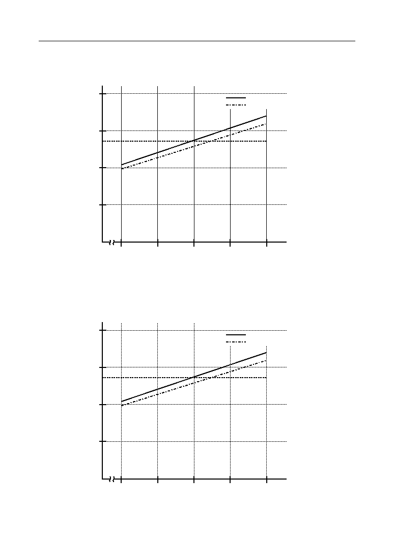
Oscillation Characteristics 1 (Rs=10k
W, C=56pF, R variable characteristics)
1/17 duty
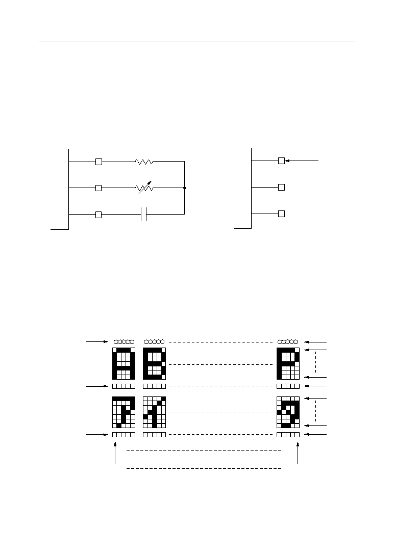
Oscillation Characteristics 2 (Rs=10k
W, R=75kW, C variable characteristics)
1/17 duty
40
30
20
10
0
55
65
75
85
95
f=80kHz,
Frame cycle•2=27.2ms
V
DD
=3.0V
V
DD
=5.0V
R Resistance (k )
Frame Cycle
•
2 (ms)
W
40
30
20
10
0
35
45
55
65
75
f=80kHz,
Frame cycle•2=27.2ms
V
DD
=3.0V
V
DD
=5.0V
C Capacitance (pF)
Frame Cycle
•
2 (ms)

8/30
° Semiconductor
MSM6665-xx
FUNCTIONAL DESCRIPTION
Pin Functional Description
∑ SI (Serial Input)
Input pin for inputting serially commands and display data in an 8-bit unit.
"H"="1" and "L"="0".
When CS pin is at "H" level, read-in is executed by the leading edge of SHT.
Whether input data is a command or data is determined by selecting a C/D level at the
8th leading edge of SHT.
The input data is a command if C/D="H", and display data if C/D="L".
∑ C/D (Command/Data)
Input pin for determining whether input data for SI pin is a command or display data.
Read-in is executed by the 8th leading edge of SHT. The input data is a command if C/
D="H", and display data if C/D="L".
∑ SHT (Shift Clock)
Clock input pin for reading-in SI input and C/D input.
Read-in is executed by the clock leading edge. Read-in operation is complete with 8
clocks. Inputting data during BUSY may cause malfunction.
Valid if CS pin is at "H" level.
∑ SO (Serial Out)
Serial output pin for reading-out BUSY/NON-BUSY and display data. "H"="1" and
"L"="0". If CS pin is at "H" level and Serial Out Enable is set with the command, output
is executed. Otherwise, this pin becomes high impedance.
BUSY/NON-BUSY is output when CS pin is at "H" level. BUSY if "L" and NON-BUSY
if "H". It goes BUSY after the 8th leading edge of SHT, then goes NON-BUSY
automatically after a specified time.
Display data is output synchronously with the leading edge of SHT.
Input the "SOE/D" instruction to set this output to serial out enable or a high impedance
state because the pin status is undefined after the power is applied.
∑ CS (Chip Select)
Chip Select input pin.
"Chip Select ON" if CS pin is at "H" level, and "Chip Select OFF" at "L" level. When "L"
level is input, SO pin becomes open and SHT pin becomes equivalent to "H" level inside
of the IC. Moreover, it prevents the input stages of SI, C/D and SHT pins from current
flowing.
* For SI, C/D, SHT, SO, and CS, refer to "I/O Procedure".
∑ RST
Direct input reset input pin.
By inputting "L" level pulse into RST pin, DISP, ABBC1/5, ABB, and BPC commands are
set as D0="0". Before turning on the power, be sure to set RST pin at "L" level once. Setting
this pin at "L" level during command execution may cause malfunction.
∑ 9D/17D (1/9Duty/1/17Duty)
Duty setting input pin.
1/9 duty is set if this pin is at "H" level, and 1/17 duty at "L" level. Choice depends on
the type of panel to be used.
9/30
° Semiconductor
MSM6665-xx
If 1/9 duty is selected, common outputs C10 to C17 should be set open.
∑ TEST1, TEST2, TEST3
Test signal input pins.
The manufacturer uses these pins for testing.
The user should connect this pin to GND or leave open.
∑ OSC1, OSC2, OSC3
Pins used for 80kHz RC oscillation circuit formation and as external master clock input
pin. Leave OSC2 and OSC3 open during input of external master clock.
∑ V
DD
, V
SS
Supply voltage pins. V
DD
should be set at "H" level.
Arbitrator
Cursor
<Relationship between panel and LCD output>
S1
S80
C17
C16
C10
C9
C8
C2
C1
Cursor
OSC1
OSC2
OSC3
10k W
76±5k W
56pF
OSC1
OSC2
OSC3
80kHz
OPEN
OPEN
[External master clock input]
[RC oscillation circuit formation]
< Oscillation circuit wiring diagram >
∑ C1 - C17, S1 - S80 (Common 1 - 17, Segment 1 - 80)
LCD output pins to be connected with the LCD panel. Turning into AC is made by frame
inversion.
Use the C1 to C9 pins during use at 1/9 duty, and leave the C10 to C17 pins open.
∆
Refer to "Relationship between panel and LCD output".

10/30
° Semiconductor
MSM6665-xx
V
SS
is a GND pin. If the battery is used, V
DD
is connected to the positive pin, and V
SS
to
the negative pin.
∑ V
SS1
, V
SS2
, V
SS3
, V
SS4
, V
SS5
LCD bias voltages input pins.
(EXAMPLE)
Case of 1/5 bias
(V
BI
=V
DD
≠V
SS5
)
Highest voltage :
V
DD
V
SS1
(V
DD
≠1/5 V
BI
)
V
SS2
(V
DD
≠2/5 V
BI
)
V
SS3
(V
DD
≠3/5 V
BI
)
V
SS4
(V
DD
≠4/5 V
BI
)
Lowest voltage :
V
SS5
Case of 1/4 bias
(V
BI
=V
DD
≠V
SS5
)
Highest voltage :
V
DD
V
SS1
(V
DD
≠1/4 V
BI
)
V
SS2
, V
SS3
(V
DD
≠2/4 V
BI
)
V
SS4
(V
DD
≠3/4 V
BI
)
Lowest voltage :
V
SS5
11/30
° Semiconductor
MSM6665-xx
List of Commands
Mnemonic
7
1
Comments
D
Serial addresses 0 to 47
1
No.
LPA
Operation
Load Pointer Address
Arbitrator Blink
LOT
BKCG 1/0
SOE/D
DISP
ABBC 1/5
ABB
AINC
CHB
CSC
CSB
CCB
BPC
Load Option
Bank Change 1/0
Serial Out Enable/Disable
Display on/off
Arbitrator Blink Control
1/5 dot
Address Increment
Character Blink on/off
Cursor Control on/off
Cursor Blink on/off
Character & Cursor
Blink on/off
Blink Pattern Control
6
1
5
A5
4
A4
3
A3
2
A2
1
A1
0
A0
Meanings for I1 and I0 are set as in
the table below.
Valid only when 1/9duty is selected.
Switching between display addresses
0 to 15 and 16 to 31.
Switching between output and high
impedance of SO
Sets arbitrator blink in a 1dot unit or
a 5dot unit. 1dot if D0="1", 5 dot if
D0="0"
1
1
1
1
1
1
1
0
0
0
0
1
0
0
0
0
0
0
0
X
X
X
X
1
0
0
0
0
0
0
X
X
X
X
0
0
1
X
X
X
1
0
X
X
X
X
X
X
X
0
0
1
1
1
1
0
0
1
1
0
X
0
1
0
1
1
X
0
1
0
1
0
I1
0
1
0
0
0
1
1/0
1/0
1/0
1/0
1
I0
1/0
1/0
1/0
1/0
1/0
X
X
X
X
X
1/0
2
3
4
5
6
7
8
9
10
11
12
13
Data that is input via SI after setting
D0="1", is set as data for arbitrator
blink (1-dot unit). This is cancelled by
D0="0"
Pointer address is incremented by 1.
Controls blinking of characters and
arbitrators (in 5 dots). Though arbitrator
blink that is set as all-blank displayed is
acceptable, blinking does not occur.
Turns cursor on or off.
Controls blinking of cursor.
But, though blinking setting with
no cursor-on setting is acceptable,
blinking does not occur.
CHB + CSB
Sets blink patterns of characters.
( :chara.) if D0="1", ( :chara.)
if D0="0"
u
s
Display ON if D0="1"
Display OFF if D0="0"
When at Display OFF, V
DD
level
voltage is output to all the COM and
SEG pins.
X : Don't care
Notes: 1. Entering commands number 1 to 7 and number 13 does not affect pointer address.
2. By entering commands number 8 to 12 or display code data, pointer address is
automatically incremented by 1.
3. When Reset is entered, commands number 5 to 7 and number 13 are set to D0="0".
I1
0
0
1
1
I0
0
1
0
1
Operation is cancelled. (No operation)
Hereafter, equivalent to writing blank code at each AINC execution.
Hereafter, cursor-off and blink-cancellation are executed at each AINC execution.
Both of above two operations are indicated.
Operation
12/30
° Semiconductor
MSM6665-xx
Command Description
[D7, D6, D5, D4, D3, D2, D1, D0], X=don't care
∑ LPA (Load Pointer Address)
[1,1,A5,A4,A3,A2,A1,A0]
The command sets "address" data into the address pointer to specify an address on
which command execution affects and an address where display data is stored. The
"address" is a number between 0H and 2FH, given by A0 through A5 in hexadecimal.
When addresses 30H through 3FH are specified, display data and CHB, CSC, CSB, CCB
commands become invalid through an address pointer is set up. Normally, the address
pointer is a loop of 0H through 2FH.
∑ LOT (Load Option)
[1,0,1,1,X,X,I1,I0]
This command indicates some specific operation of display at the current address which
is performed each time of AINC command execution.
Operation is specified by bit I1 and I0 of the command.
I0
0
1
0
Operation
1
I1
0
0
1
1
Operation is cancelled. (No operation)
Hereafter, equivalent to writing blank code at each AINC execution.
Hereafter, Cursor-off and blink-cancellation are executed at each AINC execution.
Both of above two operations are indicated.
Note) When blink-cancellation is executed, all RAM data, which controls blinks for each bit of the
arbitrator, go zeros.
∑ BKCG 1/0 (Bank Change 1/0)
[1,0,0,X,0,0,0,1/0]
Command used to do switching between display address groups (switching between
BANKs), which is valid only when 1/9duty display is selected.
When D0 is "0", display address range becomes 0 through 15, and 32 through 47.
When D0 is "1", display address range becomes 16 through 31, and 32 through 47.
Command execution and display data setting are not affected by Bank setting.
The D0 status is not changed by Reset inputting. The D0 status is unknown when the
system is powered on. So D0 must be set to "0" or "1" with the command.
∑ SOE/D (Serial Out Enable/Disable)
[1,0,0,X,0,1,1,1/0]
Command used to control the impedance of SO output pin.
When D0 is "1", display data is output via SO pin. When D0 is "0", SO pin goes to high
impedance.
The D0 status is not changed by Reset inputting. The D0 status is unknown when the
system is powered on. So D0 must be set to "0" or "1" with the command.

13/30
° Semiconductor
MSM6665-xx
∑ DISP (Display on/off)
[1,0,0,X,1,0,0,1/0]
Command used to control lighing-on and lighting-off for the LCD panel.
When D0 is "1", the display of the LCD panel goes on, and When D0 is "0", it goes off.
When the display is off, the V
DD
level voltage is output on all of pins of both the segment
driver and the common driver.
D0 is set to "0" after inputting Reset.
∑ ABBC 1/5 (Arbitrator Blink Control 1/5 dot)
[1,0,0,1,1,1,0,1/0]
Command used to do switching between arbitrator's blinking in a 1-dot unit and or in
a 5-dot unit.
When D0 is "1", arbitrator's blinking comes in the 1-dot unit mode.
When D0 is "0", it comes in the 5-dot unit mode.
D0="0" is set after inputting Reset.
Note) 1-dot unit blink setting ∆ ∑ See ABB.
5-dot unit blink setting ∆ ∑ See CHB.
∑ ABB (Arbitrator Blink)
[1,0,0,0,1,1,0,1/0]
Command used to control on/off of blinking, which is valid only when arbitrator's
blinking is set in the 1-dot unit mode.
Data , which are entered via SI pin after setting D0="1", are taken as arbitrator blink data
(1-dot unit).
Input blink data correspond to each of arbitrator's dots. When "1", blinking is on, and
when "0", blinking is off.
Note that the arbitrator, which arbitrator-on is not specified, is not able to blink, though
blink-setting is available. Dummy data must be entered into the arbitrator blink data D5
thru D7.
It is impossible to write data in addressed 00H through 31H.
D0="0" is set after inputting Reset.
Note)
If blink is set in the 5-dot unit mode, ABB command setting (D0="1" or "0") is
available, but blink-on/off setting via input of display data is impossible.
∑ AINC (Address Increment)
[1,0,0,X,1,X,1,X]
Command used to increment the value of the address pointer by 1.
The pointer is increment by 1 each time this command is executed. The operation set by
LOT command is given to the address before being increased by 1 each time this
command is execution.
14/30
° Semiconductor
MSM6665-xx
∑ CHB (Character Blink on/off)
[0,X,X,X,0,0,1/0,X]
Command used to control blinking of characters and arbitrator (5-dot unit).
This command is executed to the address indicated by the address pointer. Blinking is
on by setting D1="1", and off by setting D1="0".
For blinking of characters, all lighting-on or all lighting-off, and characters-displaying
are repeated.
Choosing between all lighting-on and all lighting-off is controlled by BPC command.
For arbitrator, only lighting bits repeat lighting-off or lighting-off. The blink control or
arbitrator is valid only when ABBC1/5="0" and in the 5-dot unit mode.
Refer to "BPC".
∑ CSC (Cursor Control on/off)
[0,X,X,X,0,1,1/0,X]
Command used to control lighting-on and lighting-off of cursor.
This command is executed to the address indicated by the address pointer.The cursor
is lighting on by setting D1="1", and lighting off by setting D1="0".
∑ CSB (Cursor Blink on/off)
[0,X,X,X,0,1,1/0,X]
Command used to control blinking of cursor.
This command is executed to the address indicated by the address pointer. Blinking is
on by setting D1="1", and off by setting D1="0".
The blinking in the address, where cursor-lighting-on is not specified, does not occur,
though the command of blinking is acceptable. Blinking starts by specifying cursor-
lighting-on.
∑ CCB (Character & Cursor Blink on/off)
[0,X,X,X,1,1,1/0,X]
Command used to execute both CHB command and CSB command.
∑ BPC (Blink Pattern Control)
[1,0,0,X,0,0,1,1/0]
Command used to control blink patterns of characters.
When D0="1" is set, all lighting-off (35 dots) and characters-displaying are repeated.
When D0="0" is set, all lighting-on (35 dots) and characters-displaying are repeated.
When D0="1" is set, if characters are blank, their blinkings do not occur in appearance.
When D0="0" is set, if characters are in all lighting-on, their blinkings do not occur in
appearance.
D0 is set to "0" affer inputting Reset.
[D0 = "1"]
[D0 = "0"]
∑ Increment (+1) in address pointer
When display data or arbitrator data (1-dot unit) is entered or when the following
commands are executed, the address pointer is incremented by 1.
AINC, CHB, CSC, CSB and CCB.
15/30
° Semiconductor
MSM6665-xx
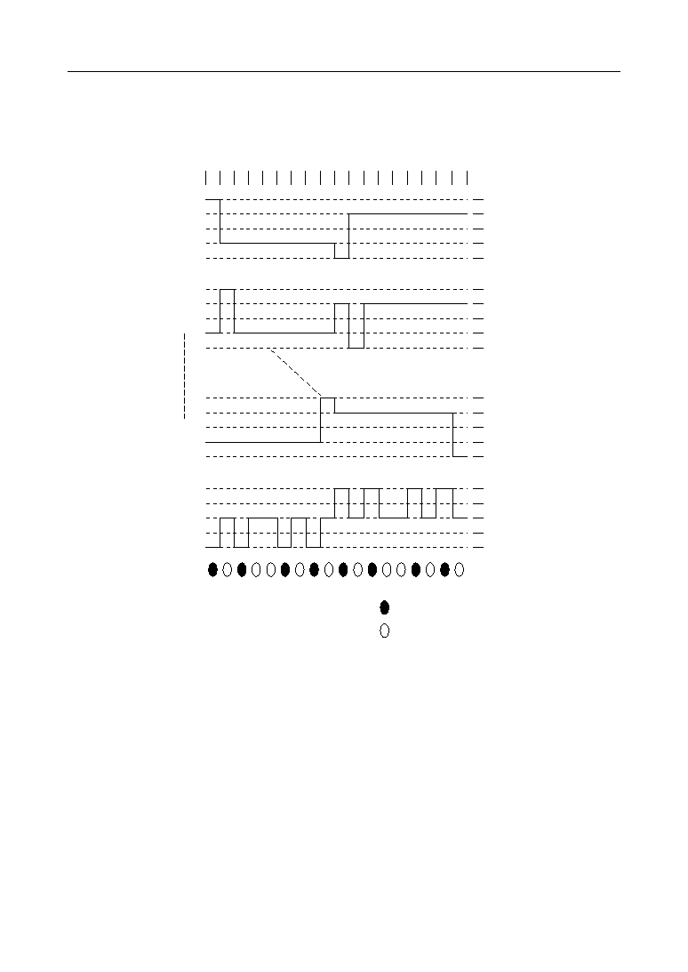
8-bit input synchronization is taken by this leading edge.
If input in an 8-bit unit is kept, the following leading edges of CS is not needed.
17D : Max=[Master clock cycle] x 10
9D : Max=[Master clock cycle] x 20
BUSY
LSB
MSB
BUSY
"Z"
don't care
C/D
C / D
C S
S O
S I
SHT
NON-BUSY/
I/O Procedure
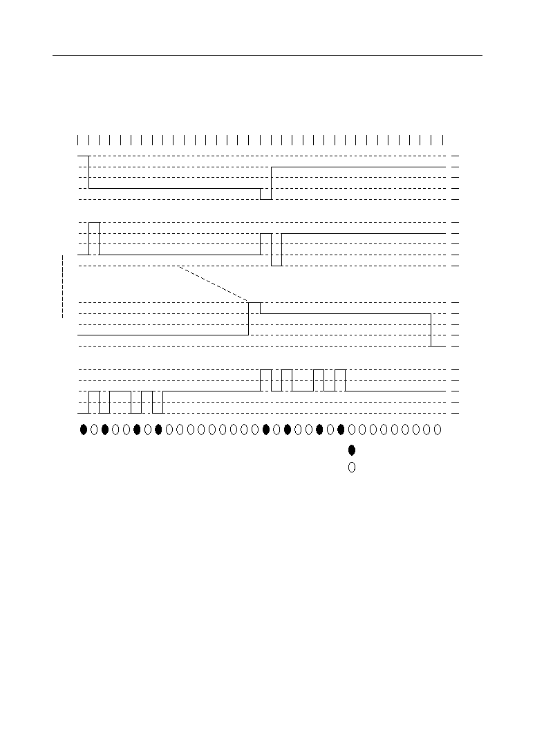
∑ Input timing (command input, display data input)
∑ Output timing (display code data output)
Code data or arbitrator data indicated by the address pointer is always output, provided
that the SOE command has already been input.
BUSY
LSB
MSB
NON-BUSY/ BUSY
"Z"
don't care
C / D
C S
S O
SHT
Synchronization in an 8-bit unit.
17D : Max=[Master clock cycle] x 10
9D : Max=[Master clock cycle] x 20
NON-BUSY
Note) If CS is set at "L" level when 8-bit read-out is not complete, and CS is set at "H" level again, then
read-out operation is executed, uncomplete data will be output continually and the remaining
read-out data will be zero.

16/30
° Semiconductor
MSM6665-xx
Method of Calculating Various Types of Frequencies
∑ Original Clock Frequency and Blink Frequency
Blink cycle calculation
([Original clock cycle] x 5) x 2
14
= Blink cycle ............................................. Formula 1
From formula 1, the blink frequency can be calculated.
Example) When the original clock is 80kHz:
Clock cycle Ts=12.5 [
µ
s]
From formula 1,
Blink cycle Tb=(12.5 x 10
-6
x 5) x 2
14
= 1.024 [s]
Thus,
Blink frequency = 1 [Hz]
∑ Original Clock Frequency and Frame Frequency
Frame cycle calculation
1/9 DUTY: (Original clock cycle) x 1152 = Frame cycle ............................. Formula 2
1/17 DUTY: (Original clock cycle) x 1088 = Frame cycle ........................... Formula 3
From formulas 2 and 3, the frame frequency can be calculated.
Example) In the original clock 80kHz and 1/17 DUTY specifications:
Clock cycle Ts=12.5 [
µ
s]
From formula 3,
Frame cycle Tf=12.5 x 10
-6
x 1088 = 13.6 [ms]
Thus,
Frame frequency = 73.5 [Hz]
17/30
° Semiconductor
MSM6665-xx
Display and Memory Address
Arbitrator
Character 1
Cursor 1
47
15
15
31
31
32
0
0
16
16
33
1
1
17
17
Display
RAM map
Character 2
Cursor 2
Arbitrator
Character 1
Cursor 1
Character 2
Cursor 2
Note Characters are entered with codes.
Arbitrator is displayed with no CG ROM. The relationship between input data and display is shown
below.
Dummy input is required for serial data D7 through D5.
Either "1" or "0" is available for data to be input into D7 through D5.
S5n+1
D4
D0
n : 0-15
S5n+5

18/30
° Semiconductor
MSM6665-xx
Flowchart for Power-On Timing
Turn on power
Reset input
5ms required; external reset input or power-on reset input
CS="H"
The device is enabled.
SOE/D, D0="1"
Make the SO output enable, to perform busy detection.
Wait for 20 clocks
Input a wait for the SOE/D command processing. (For the processing
of each command after this, perform busy detection. *1)
BPC and BKCG
command set
Set the blink pattern and bank change mode.
LOT, I1="1", I0="1"
Set the Load Option. (Blank-code writing and blink-cancellation
are executed each time the AINC command is executed.)
AINC executed 48 times
Input the AINC command to clear the RAM data.
LOT, I1="0", I0="0"
Release the Load Option.
Input display data for initial screen
DISP, D0="1"
Display is turned on and the initial screen is displayed.
Is Input of display data for
initial screen completed?
NO
YES
Normal operation
*1
After the required commands and display data are entered, perform busy detection
based on the SO pin status. When it is confirmed that the status has been changed
from BUSY (SO="L") to NON-BUSY (SO="H"), enter the next data.
If busy detection is not performed, wait for 10 master oscillation clocks when used at
1/17 duty or for 20 master oscillation clocks when at 1/9 duty, then enter the next
data.
19/30
° Semiconductor
MSM6665-xx
Waveforms Applied to LCD
1/17 duty (1/5 bias)
V
DD
V
SS1
V
SS2
V
SS3
V
SS4
V
SS5
1 2 3 4 5 6 7 8 9 10 11 12 13 14 15 16 17 1 2 3 4 5 6 7 8 9 10 11 12 13 14 15 16 17
V
DD
V
SS1
V
SS2
V
SS3
V
SS4
V
SS5
V
DD
V
SS1
V
SS2
V
SS3
V
SS4
V
SS5
V
DD
V
SS1
V
SS2
V
SS3
V
SS4
V
SS5
C1
C2
C17
Sn
= lighting on
= lighting off
20/30
° Semiconductor
MSM6665-xx
1/9 duty (1/4 bias)
V
DD
V
SS1
V
SS2, 3
V
SS4
V
SS5
1 2 3 4 5 6 7 8 9 1 2 3 4 5 6 7 8 9
C1
C2
C9
Sn
= lighting on
= lighting off
V
DD
V
SS1
V
SS2, 3
V
SS4
V
SS5
V
DD
V
SS1
V
SS2, 3
V
SS4
V
SS5
V
DD
V
SS1
V
SS2, 3
V
SS4
V
SS5
21/30
° Semiconductor
MSM6665-xx
V
DD
V
SS1
V
SS2, 3
V
SS4
V
SS5
1 2 3 4 5 6 7 8 9 10 11 12 13 14 15 16 17
C1
C2
C17
Sn
= lighting on
= lighting off
V
DD
V
SS1
V
SS2, 3
V
SS4
V
SS5
V
DD
V
SS1
V
SS2, 3
V
SS4
V
SS5
V
DD
V
SS1
V
SS2, 3
V
SS4
V
SS5
1 2 3 4 5 6 7 8 9 10 11 12 13 14 15 16 17
1/17 duty (1/4 bias)
22/30
° Semiconductor
MSM6665-xx
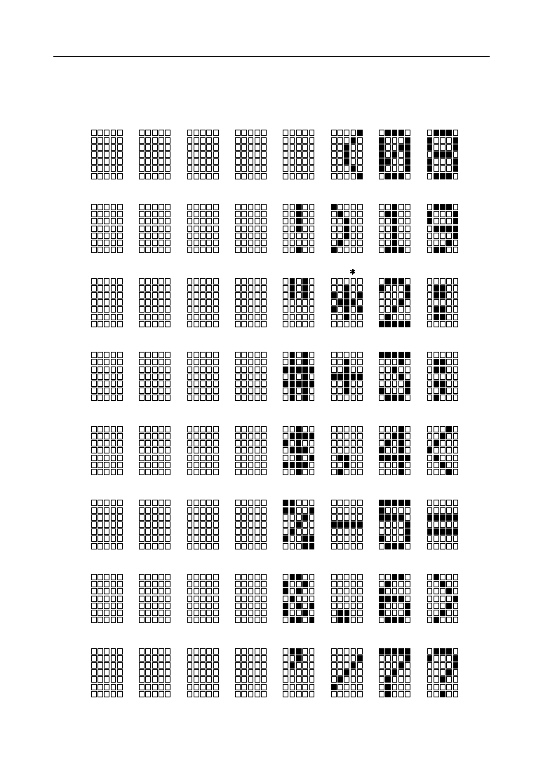
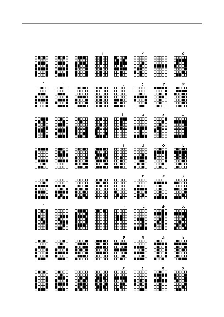
Codes and Character Fonts of Code -01
00H :
08H :
10H :
18H :
20H : SP
28H : (
30H : 0
38H : 8
01H :
09H :
11H :
19H :
21H : !
29H : )
31H : 1
00H : 9
02H :
0AH :
12H :
1AH :
22H : "
2AH :
32H : 2
3AH : :
03H :
0BH :
13H :
1BH :
23H : #
2BH : +
33H : 3
3BH : ;
04H :
0CH :
14H :
1CH :
24H : $
2CH : ,
34H : 4
3CH : <
05H :
0DH :
15H :
1DH :
25H : %
2DH : ≠
35H : 5
3DH : =
06H :
0EH :
16H :
1EH :
26H : &
2EH : .
36H : 6
3EH : >
07H :
0FH :
17H :
1FH :
27H : '
2FH : /
37H : 7
3FH : ?
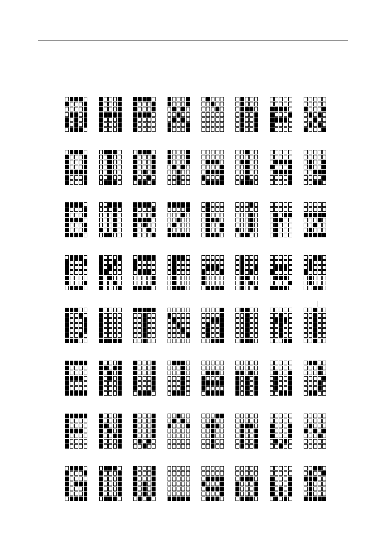
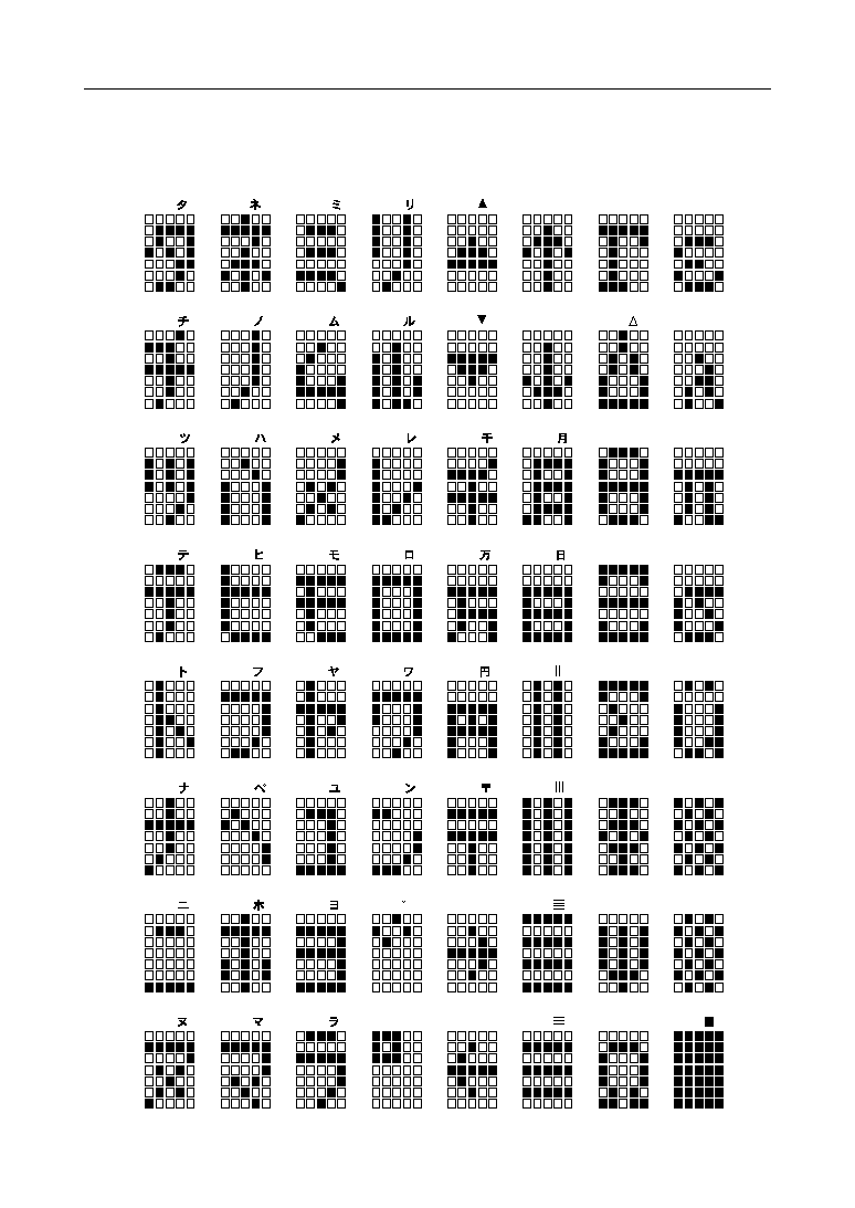
23/30
° Semiconductor
MSM6665-xx
40H : @
48H : H
50H : P
58H : X
60H : `
68H : h
70H : p
78H : x
41H : A
49H : I
51H : Q
59H : Y
61H : a
69H : i
71H : q
79H : y
42H : B
4AH : J
52H : R
5AH : Z
62H : b
64H : j
72H : r
7AH : z
43H : C
4BH : K
53H : S
5BH : [
63H : c
6BH : k
73H : s
7BH : {
44H : D
4CH : L
54H : T
5CH :
64H : d
6CH : I
74H : t
7CH :
45H : E
4DH : M
55H : U
5DH : ]
65H : e
6DH : m
75H : u
70H : }
46H : F
4EH : N
56H : V
5EH : ^
66H : f
6EH : n
76H : v
7EH : ~
47H : G
4FH : O
57H : W
5FH : _
67H : g
6FH : o
77H : w
7FH : £
/
24/30
° Semiconductor
MSM6665-xx
8ÿH : ƒ
88H : ‰
9ÿH : n
98H :
A0H : •
A8H :
B0H : --
B8H :
81H : A
89H : a
91H : ˆ
99H : i
A1H :
49H :
B1H :
B9H :
82H : ∆
8AH : ý
92H : Ÿ
9AH : ø
A2H :
AAH :
B2H :
BAH :
83H : «
93H : ¸
9BH : ß
A3H :
ABH :
B3H :
BBH :
84H : …
8CH : Ê
94H : a
9CH : ∞
A4H :
aCH :
B4H :
BCH :
85H : N
8DH : Á
95H : b
9DH : ®
A5H :
ADH :
B5H :
BDH :
86H : ÷
8EH : È
96H : ÿ
9EH : ∫
A6H :
AEH :
B6H :
BEH :
87H : Ð
8FH : Ë
97H : ¯
9FH : ¢
27H :
2FH :
37H :
3FH :
8BH : a
25/30
° Semiconductor
MSM6665-xx
CÿH :
C8H :
DÿH :
D8H :
EÿH :
E8H :
FÿH : G
F8H : e
C1H :
C9H :
D1H :
D9H :
E1H :
E9H : ÿ
F1H :
F9H :
l
C2H :
CAH :
D2H :
DAH :
E2H :
EAH :
F2H : q
FAH : p
C3H :
D3H :
DBH :
E3H :
EBH :
F3H : X
FBH : s
C4H :
CCH :
D4H :
DCH :
E4H :
ECH :
F4H : S
FCH : ¸
C5H :
CDH :
D5H :
DDH :
E5H :
EDH :
F5H : F
FDH :
C6H :
CEH :
D6H :
DEH :
E6H : ∆
EEH :
FEH : Y
FEH :
C7H :
CFH :
D7H :
DFH : ∞
E7H : ®
EFH :
F7H : W
FFH :
CBH :
26/30
° Semiconductor
MSM6665-xx
APPLICATION CIRCUIT
Example :
1/17 duty, 1/5 bias
Cursor-contained (5 x 7 dot )16-character x 2-line LCD panel
COM
SEG
17 dot
80 dot
LCD bias
or
OSC1
OSC2
OSC3
80kHz
10kW
56pF
OSC1
OSC2
OSC3
M S M 6 6 6 5 - x x
V
Vss
1
Vss
2
Vss
3
Vss
4
Vss
5
9D/
17D
Vss
TEST
CS
C/
SHT
SO
SI
D
RST
PORT
OPEN
OPEN
1-3
DD
C1-C17
S1
-
S80
75kW
Bias Generation Circuit
27/30
° Semiconductor
MSM6665-xx
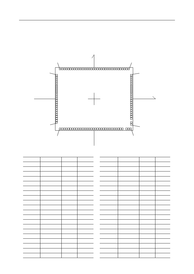
PAD CONFIGURATION
Pad layout
Chip size : 6.05 • 4.98mm
Passivation film etched hole : 110 • 110mm
92
93
117
1
33
34
X
58
59
Y
C15
≠2486
≠2332
Pad Name
X (mm)
Y (mm)
Pad No.
Pad Name
X (mm)
Y (mm)
C14
≠2336
≠2332
C13
≠2186
≠2332
C12
≠2036
≠2332
C11
≠1886
C10
≠1736
C9
≠1586
C8
≠1436
C7
≠1286
C6
≠1136
C5
C4
C3
C2
C1
V
SS
V
SS5
V
SS4
V
SS3
≠986
≠836
≠686
≠536
≠386
≠227
≠67
83
233
21
V
SS1
533
≠2332
22
CS
683
23
C/D
833
24
SI
983
25
SHT
1133
26
9D/17D
1283
27
RST
1433
28
SO
1583
29
V
DD
1733
30
31
32
33
34
35
36
37
38
39
OSC1
OSC2
OSC3
TEST1
TEST2
TEST3
S80
S79
S78
S77
1891
2308
2789
2659
2870
2870
2870
2870
2870
2870
V
SS2
383
40
S76
2870
≠2332
≠2332
≠2332
≠2332
≠2332
≠2332
≠2332
≠2332
≠2332
≠2332
≠2332
≠2332
≠2332
≠2332
≠2332
≠2332
≠2332
≠2332
≠2332
≠2332
≠2332
≠2332
≠2332
≠2332
≠2332
≠2332
≠2332
≠2332
≠1797
≠1647
≠1347
≠1197
≠1047
≠897
≠747
1
Pad No.
2
3
4
5
6
7
8
9
10
11
12
13
14
15
16
17
18
19
20
Pad Coordinates
28/30
° Semiconductor
MSM6665-xx
Pad No.
Pad Name
X (mm)
Y (mm)
Pad Name
X (mm)
Y (mm)
41
S75
2870
≠567
42
S74
2870
≠447
43
S73
2870
≠297
44
S72
2870
≠147
45
S71
2870
3
46
S70
2870
153
47
S69
2870
303
48
S68
2870
453
49
S67
603
50
51
52
53
54
55
56
57
58
59
S66
S65
S64
S63
S62
S61
S60
S59
S58
S57
753
903
1053
1203
1353
1503
1653
1803
1953
2332
2332
2332
60
61
62
63
64
65
66
67
68
69
S56
S55
S54
S53
S52
S51
S50
S49
S48
S47
2332
2332
2332
2332
2332
2332
2332
2332
70
71
72
73
74
75
76
77
78
79
S46
S45
S44
S43
S42
S41
S40
S39
S38
S37
2332
2332
2332
2332
2332
2332
≠68
≠218
≠368
≠518
≠668
S36
S35
≠818
2332
S34
≠968
S33
≠1118
S32
≠1268
S31
≠1418
S30
≠1568
S29
≠1718
S28
≠1868
S27
≠2018
S26
S25
S24
S23
S22
S21
S20
S19
S18
S17
≠2168
≠2318
≠2468
≠2870
≠2870
≠2870
≠2870
≠2870
≠2870
≠2870
≠2870
≠2870
≠2870
≠2870
S16
S15
S14
S13
S12
S11
S10
S9
S8
S7
≠2870
≠2870
≠2870
≠2870
≠2870
≠2870
S6
S5
S4
S3
S2
S1
C17
C16
≠2870
≠2870
≠2870
≠2870
≠2870
≠2870
≠2870
≠2870
2870
2870
2870
2870
2870
2870
2870
2870
2870
2870
2482
2332
2182
2032
1882
1732
1582
1432
1282
1132
982
832
682
532
382
232
82
2332
2332
2332
2332
2332
2332
2332
2332
2332
2332
2332
2332
2332
2332
2332
2332
1803
1653
1503
1353
1203
1053
903
753
603
453
303
153
3
≠147
≠297
≠447
≠597
≠747
≠897
≠1047
≠1197
≠1347
≠1497
≠1647
≠1797
Pad No.
81
82
83
84
85
86
87
88
89
90
91
92
93
94
95
96
97
98
99
100
101
102
103
104
105
106
107
108
109
110
111
112
113
114
115
116
117
80
29/30
° Semiconductor
MSM6665-xx
Pin and Pad Correspondence
The symbol for each chip pad and package pin is equal, but the numbers for each pad and pin
are not equal.
If both chips and packaged devices are used, the number for each chip pad should be
corresponded to the number for each package pin according to each symbol listed in the table
below.
Symbol
Chip Package
Pad
Pin
C15
1
65
Symbol
Chip Package
Pad
Pin
OSC2
31
100
Symbol
Chip Package
Pad
Pin
S55
61
3
Pad
Pin
S25
37
C14
2
66
OSC3
32
101
S54
62
4
S24
91
38
C13
3
67
TEST1
33
102
S53
63
5
S23
92
39
C12
4
68
TEST2
34
103
S52
64
6
S22
93
40
C11
5
69
TEST3
35
104
S51
65
7
S21
94
41
C10
6
70
S80
36
106
S50
66
8
S20
95
42
C9
7
71
S79
37
107
S49
67
9
S19
96
43
C8
8
72
S78
38
108
S48
68
10
S18
97
44
C7
9
73
S77
39
109
S47
69
11
S17
98
45
C6
10
74
S76
40
110
S46
70
12
S16
99
46
C5
11
75
S75
41
111
S45
71
14
S15
100
47
C4
12
76
S74
42
112
S44
72
15
S14
101
48
C3
13
78
S73
43
113
S43
73
17
S13
102
49
C2
14
79
S72
44
114
S42
74
18
S12
103
50
C1
15
81
S71
45
115
S41
75
19
S11
104
51
V
SS
(GND)
16
82
S70
46
116
S40
76
20
S10
105
52
V
SS5
17
83
S69
47
117
S39
77
21
S9
106
53
V
SS4
18
84
S68
48
118
S38
78
22
S8
107
54
V
SS3
19
85
S67
49
119
S37
79
24
S7
108
55
V
SS2
20
86
S66
50
120
S36
80
25
S6
109
56
V
SS1
21
88
S65
51
121
S35
81
27
S5
110
57
CS
22
89
S64
52
122
S34
82
28
S4
111
58
C/D
23
91
S63
53
123
S33
83
29
S3
112
59
SI
24
92
S62
54
124
S32
84
30
S2
113
60
SHT
25
93
S61
55
125
S31
85
31
S1
114
61
9D/17D
26
94
S60
56
126
S30
86
32
C17
115
62
RST
27
95
S59
57
127
S29
87
33
C16
116
63
SO
28
96
S58
58
128
S28
88
34
117
≠
V
DD
29
97
S57
59
1
S27
89
35
≠
≠
OSC1
30
98
S56
60
2
S26
90
36
≠
≠
≠
≠
≠
≠
Symbol
Chip Package

30/30
° Semiconductor
MSM6665-xx
(Unit : mm)
PACKAGE DIMENSIONS
Notes for Mounting the Surface Mount Type Package
The SOP, QFP, TSOP, SOJ, QFJ (PLCC), SHP and BGA are surface mount type packages, which
are very susceptible to heat in reflow mounting and humidity absorbed in storage.
Therefore, before you perform reflow mounting, contact Oki's responsible sales person for the
product name, package name, pin number, package code and desired mounting conditions
(reflow method, temperature and times).
QFP128-P-1420-0.50-K
Package material
Lead frame material
Pin treatment
Solder plate thickness
Package weight (g)
Epoxy resin
42 alloy
Solder plating
5 mm or more
1.19 TYP.
Mirror finish