° Semiconductor
1/9
MSM6685A
° Semiconductor
MSM6685A
8,388,608-Word x 1-Bit Serial Register
This version: Feb. 1999
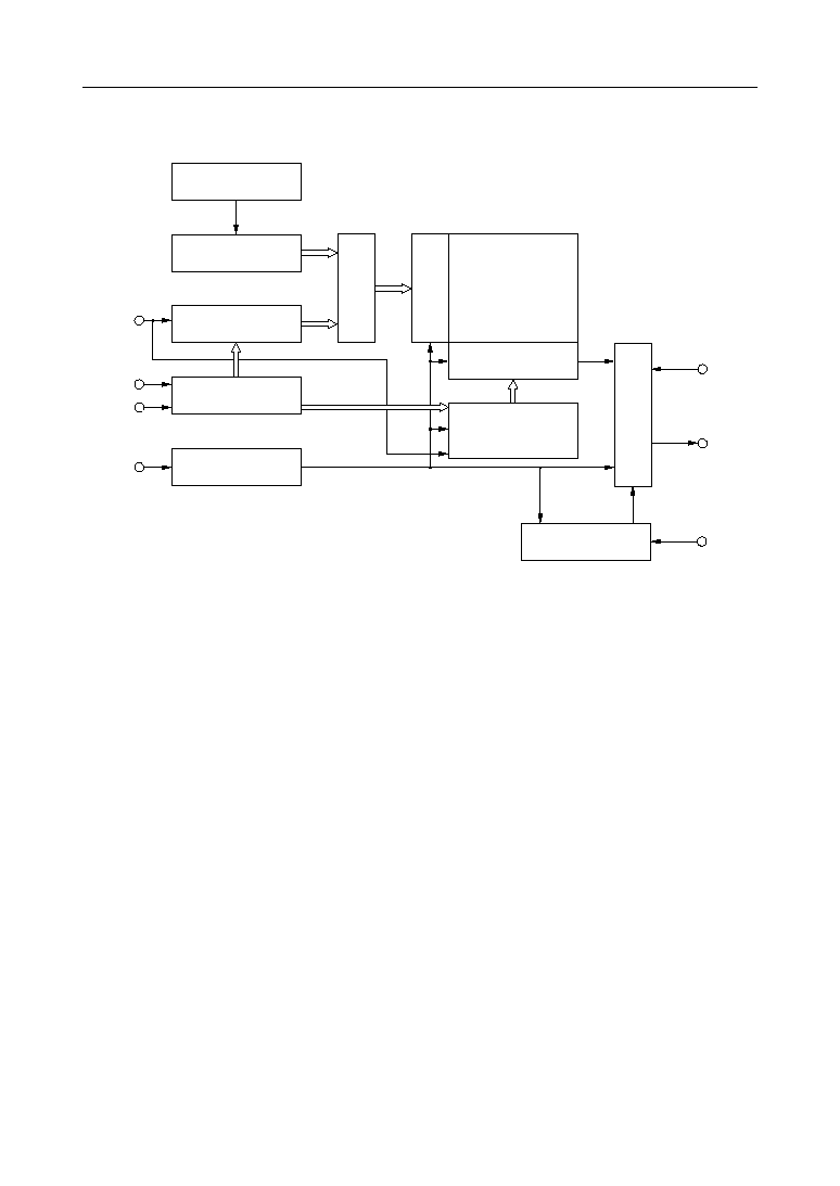
GENERAL DESCRIPTION
The MSM6685A is a serial register composed of 8,388,608 words x one bit, characterized by medium-
speed, low power consumption operation.
This device has a built-in internal address generation circuit allowing continuous serial read/write
operation by external clock input. Read/write operation causes the internal address to be incremented
automatically by +1.
External address input enables addressing in units of 1024 words. Furthermore, a refresh timer and
a refresh address counter are installed, which makes an external refresh circuit unnecessary. In
addition, this configuration allows lower power consumption.
The device is packaged in 26-pin SOJ having a width of 300 mil.
It is well adapted for storing much data by means of a battery backup. Its combination with OKI's
recording and playback IC enables the easy implementation of a solid recording and playback
system.
FEATURES
∑ Configuration
: 8,388,608 • 1 bit
∑ Serial access operation
Serial access time
: 1.5 ms
Serial read/write time
: 2.5 ms
∑ Low current drain
: 200 mA max. (V
CC
= 4 V, at refresh operation, with
data stored and under standard conditions)
∑ Refresh operation
A self-refresh function is supported.
∑ Wide range of operating voltage
: Single 3.5 to 5.5 V supply
∑ Addressing
: In units of 1024 words
∑ Process
: 0.45 mm double well CMOS process
∑ Package:
26/20-pin plastic SOJ (SOJ26/20-P-300-1.27) (Product name : MSM6685AJS)
E2D0109-19-21
° Semiconductor
3/9
MSM6685A
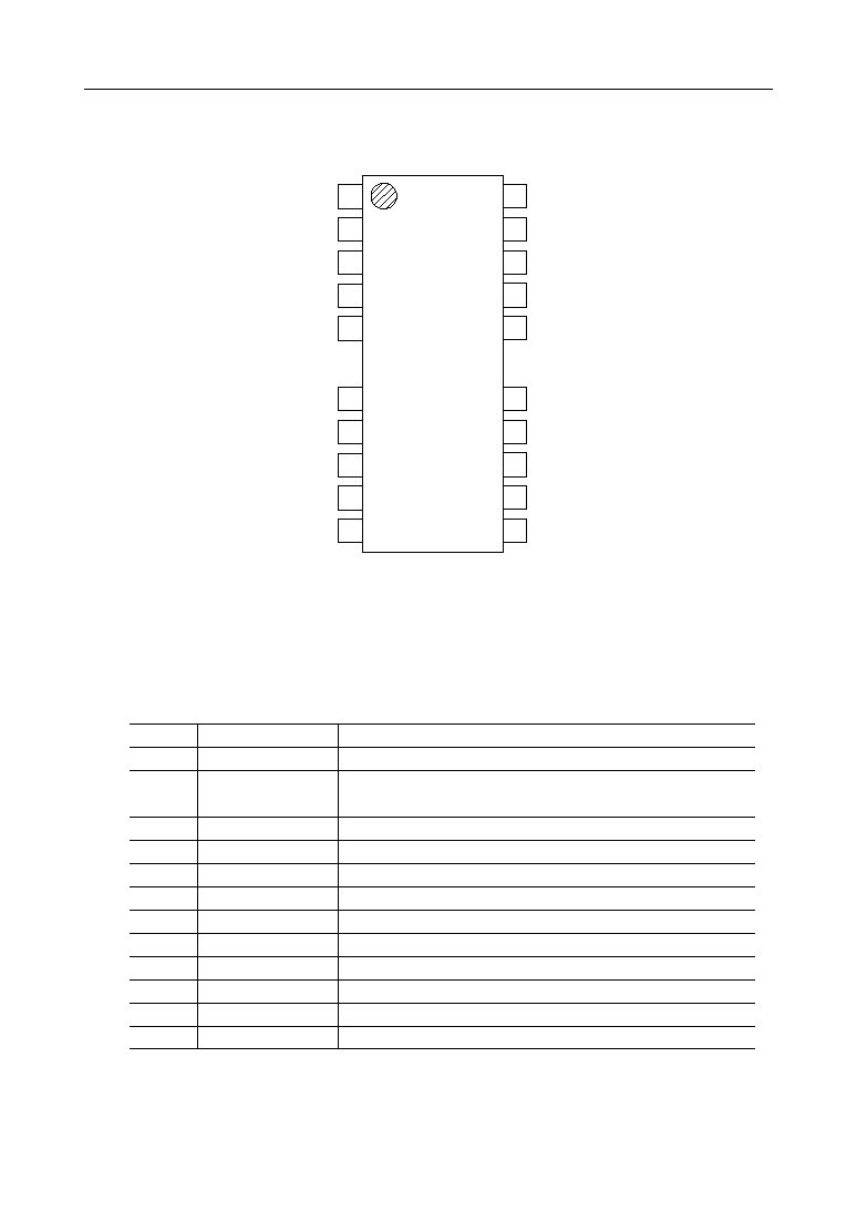
PIN CONFIGURATION (TOP VIEW)
NC : No connection
26/20-Pin Plastic SOJ
TEST
RWCK
NC
TEST
TEST
V
SS
NC
DIN
TEST
TEST
1
2
3
4
5
9
10
11
12
13
V
CC
26
TEST
25
TEST
24
SAD
23
SAS
22
NC
14
DOUT
15
WE
16
CS
17
TAS
18
PIN DESCRIPTION
Note : All TEST pins are to be connected to the power supply.
The TEST pin is to be referenced to the ground level.
Test input
Pin
Description
25
Test input
1, 4, 5
9, 10, 24
Read/write clock
2
Data input
11
Ground (0 V)
13
Data output
15
Write enable
16
Chip select
17
Transfer address strobe
18
Serial address strobe
22
Serial address data
23
Power supply (5 V)
26
Symbol
TEST
TEST
RWCK
DIN
V
SS
DOUT
WE
CS
TAS
SAS
SAD
V
CC
° Semiconductor
4/9
MSM6685A
ABSOLUTE MAXIMUM RATINGS
Parameter
Symbol
Condition
Rating
Unit
Pin Voltage
V
T
Against V
SS
at Ta = 25 ∞C
≠1.0 to +7.0
V
Short-circuit Output Current
Ta = 25 ∞C
50
mA
Power Dissipation
1
W
Operating Temperature
--
0 to 70
∞C
Storage Temperature
--
≠55 to +150
∞C
I
OS
P
D
T
op
T
STG
Ta = 25 ∞C
RECOMMENDED OPERATING CONDITIONS
Parameter
Symbol
Min
Typ
Max
Unit
Supply Voltage
V
CC
3.5
4.5
5.5
Supply Voltage
0
0
0
"H" Input Voltage
V
CC
≠ 0.5
V
CC
V
CC
+ 0.2
"L" Input Voltage
≠0.2
0
+0.5
V
V
V
V
V
SS
V
IH
V
IL
(Ta = 0 to 70∞C)
ELECTRICAL CHARACTERISTICS
DC Characteristics
Parameter
Symbol
Condition
Min
Max
Unit
"H" Output Voltage
V
OH
I
OH
= ≠0.5 mA
V
CC
≠ 0.5
--
V
"L" Output Voltage
I
OL
= 0.5 mA
--
0.4
V
Input Leakage Current
I
IL
V
I
= 0 V to V
CC
≠1
+1
mA
Output Leakage Current
V
O
= 0 V to V
CC
≠1
+1
mA
Supply Current (Operation)
V
CC
= 4 V, t
RWC
= 1 ms
--
20
mA
Supply Current (Standby)
V
CC
= 4 V
--
200
mA
V
OL
I
OL
I
CC1
I
CC2
(V
CC
= 3.5V to 5.5V, Ta = 0 to 70∞C)
° Semiconductor
5/9
MSM6685A
AC Characteristics
Parameter
Symbol
Min
Max
Unit
Read/Write Cycle Time
t
RWC
2,500
--
ns
Access Time
t
ACC
--
1,500
ns
Output Turn-off Delay Time
t
OFF
0
50
ns
I/O Signal Rise Time
t
T
3
50
ns
RWCK Pre-charge Time
t
RWP
1,000
--
ns
SAS Cycle Time
t
RW
1,500
10,000
ns
SAS Pre-charge Time
t
SSC
100
--
ns
SAS Pulse Duration
t
SAP
50
--
ns
Address Setup Time
t
SAS
50
--
ns
Adress Hold Time
t
AS
0
--
ns
TAS Setup Time
t
AH
50
--
ns
TAS . RWCK Setup Time
t
ATS
50
--
ns
TAS Pulse Duration
t
TRS
50
--
ns
Read Instruction Setup Time
t
TAS
50
--
ns
Read Instruction Hold Time
t
RRS
0
--
ns
Write Instruction Setup Time
t
RRH
250
--
ns
Write Instruction Hold Time
t
WRS
0
--
ns
Write Instruction Pulse Duration
t
WRH
50
--
ns
WE. RWCK Read Time
t
WP
50
--
ns
Data Setup Time
t
RWL
50
--
ns
Data Hold Time
t
DS
0
--
ns
RWCK. WE Delay Time
t
DH
50
--
ns
t
RWD
50
--
ns
RWCK Pulse Time
(V
CC
= 3.5 V to 5.5 V, Ta = 0 to 70∞C)