PEDL66579-03
1Semiconductor
This version: Nov. 1999
MSM66579 Family
Preliminary
16-Bit Microcontroller
1/37
GENERAL DESCRIPTION
The MSM66579 family of highly functional CMOS 16-bit single chip microcontrollers utilizes the nX-8/500S,
Oki's proprietary CPU core.
Four channels of serial ports, consisting of two channels of synchronous serial ports with 32-byte FIFO registers
and two channels of UART/synchronous serial ports, enable easy interfacing with external peripheral LSI devices
such as an encoder/decoder or servocontroller.
A switching function permits selection of separate address and data lines or multiplexed lines for the bus interface
to correspond to various peripheral LSI devices.
With features such as a clock gear function, dual clock function, programmable pull-up ports in which individual
bits can be programmed, and a small, thin package, the MSM66579 family of microprocessors is optimally suited
for the system control of small-sized low power devices.
The flash ROM versions (MSM66Q577L and MSM66Q579L) programmable with a single 2.7V (minimum)
power supply and flash ROM version (MSM66Q577) programmable with a single 5V power supply are also
included in the family. These versions are easily adaptable to quick specification changes and to new product
revisions.
APPLICATIONS
Digital Audio Control Systems
PC peripheral Control Systems
Office Electronics Control Systems
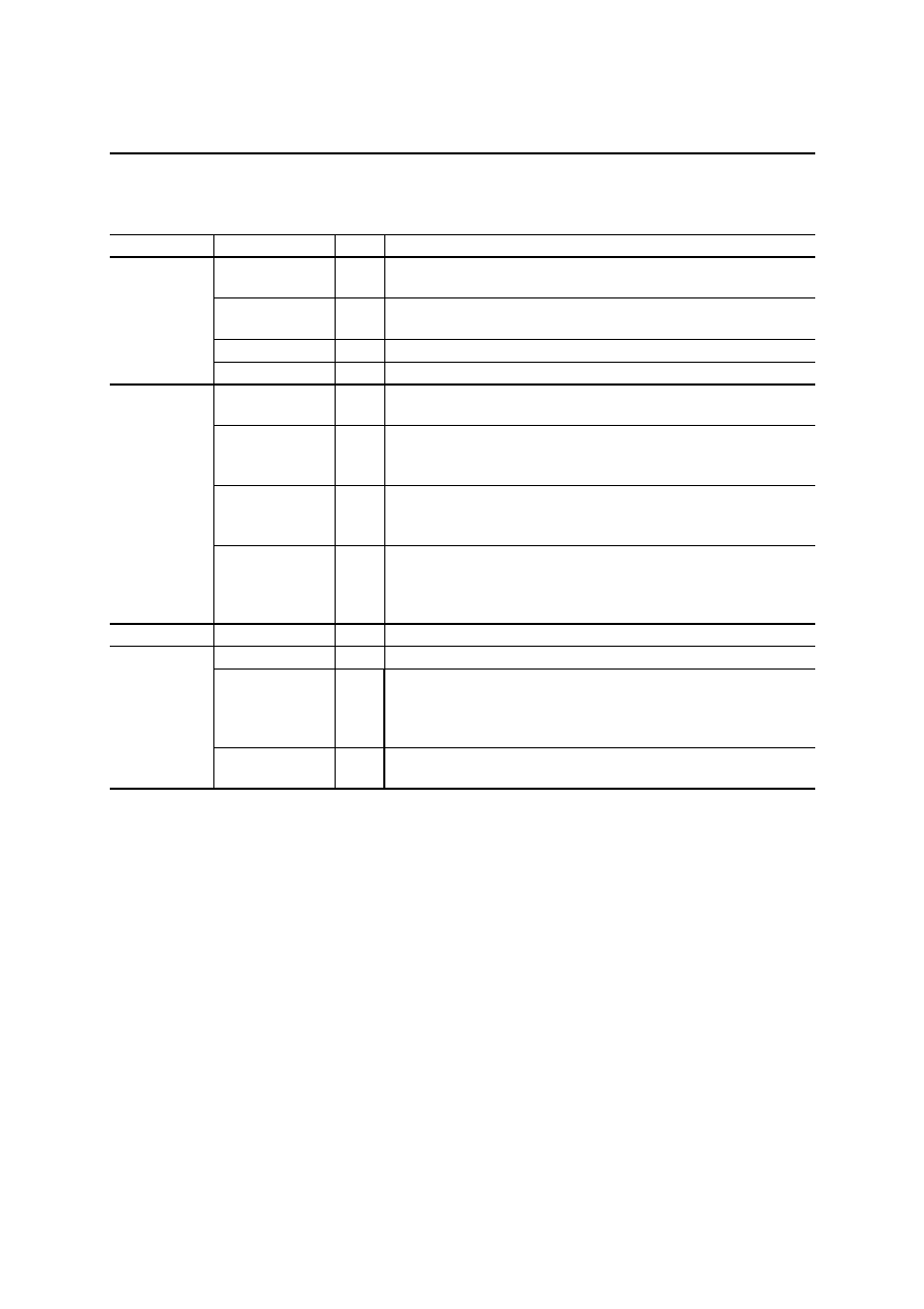
ORDERING INFORMATION
Order Code or Product Name
Package
Remark
MSM66577L-TB
Low voltage mask ROM version
(2.4 to 3.6 V)
MSM66577-TB
5 V mask ROM version
MSM66Q577L-TB
MSM66577L flash ROM version
MSM66Q577-TB
MSM66577 flash ROM version
MSM66579L-TB
Low voltage mask ROM version
(2.4 to 3.6 V)
MSM66Q579L-TB
100-pin plastic TQFP
(TQFP 100-P-1414-0.50-K)
MSM66579L flash ROM version
PEDL66579-03
1Semiconductor
MSM66579 Family
2/37
FEATURES
Name
MSM66577L
MSM66577
MSM66579L
Operating temperature
�30�C to +70�C
Power supply voltage/
maximum frequency
V
DD
= 2.4 to 3.6 V/f = 14 MHz V
DD
= 4.5 to 5.5 V/f = 30 MHz V
DD
= 2.4 to 3.6 V/f = 28 MHz
Minimum instruction
execution time
143 ns at 14 MHz
61 �s at 32.768 kHz
67 ns at 30 MHz
61 �s at 32.768 kHz
71 ns at 28 MHz
61 �s at 32.768 kHz
Internal ROM size
(max. external)
128 KB (1 MB)
Internal RAM size
(max. external)
4 KB (1 MB)
12 KB (1 MB)
I/O ports
74 I/O pins (with programmable pull-up resistors) 8 input-only pins
16-bit free running timer � 1ch
Compare out/capture input � 2ch
16-bit timer (auto reload/timer out) � 1ch
8-bit auto reload timer � 2ch (can also be used as 16-bit timer � 1ch)
8-bit auto reload timer � 1ch
8-bit auto reload timer � 3ch
(also functions as serial communication baud rate generator)
8-bit auto reload timer � 1ch (also functions as watchdog timer)
Watch timer (Real-timer counter) � 1ch
Timers
8-bit PWM � 4ch (can also be used as 16-bit PWM � 2ch)
Synchronous, with 32-byte FIFO � 2ch
Serial port
UART/Synchronous � 2ch
A/D converter
10-bit A/D converter � 8ch
D/A converter
8-bit D/A converter � 2ch
External interrupt
Non-maskable � 1ch
Maskable � 8ch
Interrupt priority
3 levels
Separate address and data busses/multiplexed address and data busses
Bus release function
Others
Dual clocks
Flash ROM version
MSM66Q577L
MSM66Q577
MSM66Q579L
PEDL66579-03
1Semiconductor
MSM66579 Family
3/37
SPECIAL FEATURES
1. High-performance CPU
The family includes the high-performance CPU, powerful bit manipulation instruction set, full symmetrical
addressing mode, and ROM WINDOW function, and also provides the best optimized C compiler support.
2. A variety of power saving modes
Attaching a 32.768-kHz crystal produces a real-time clock signal from the internal clock timer. Use of a single
clock in place of dual clocks is possible. Switching the CPU clock to this clock signal, 1/2
�
main clock, or 1/4
�
main clock, then produces operation in a low power consumption mode. The clock gear function allows a 1/2
�
or
1/4
�
main clock to be selected for the CPU operating clock.
The family provides a wide range of standby control functions. In addition to the usual STOP mode that stops the
oscillator, there are the quick restart STOP mode that shuts down the CPU and peripherals but leaves the oscillator
running, and the HALT mode that shuts down the CPU but leaves the peripherals running.
3. Variety of multifunctional serial ports
The family includes two channels of built-in synchronous serial ports with 32-byte FIFO implementing an auto
transfer function. The family allows multi-byte 1-frame information which consists of address, command, and data
to be easily and efficiently transmitted to or received from a serial interface type peripheral LSI device. The family
also allows multi-byte character information to be easily and efficiently transmitted to or received from an LCD
module. In addition, the family has two channels of combined UART/synchronous serial ports, and provides four
channels of serial interfaces.
4. MSM66Q577L, MSM66Q577 and MSM66Q579L with flash memory programmable with single power
supply
In addition to the regular mask ROM version, the family includes these versions with 128KB of flash memory that
can be programmed using a single power supply. For the MSM66Q577L and MSM66Q579L, an internal booster
circuit derives the necessary program voltage from the device's low (2.7 V min) power supply, and the program
voltage for the MSM66Q577 is provided with a single 5 V power supply.
5. High-precision A/D and D/A converters
The family includes a high-precision 10-bit analog-to-digital converter with eight channels and 8-bit digital-to-
analog converter with two channels.
6. Multifunction PWM
The family supports both 8- and 16-bit PWM operation. Choosing between the time-base counter output or
overflow from an 8-bit auto-reload timer as the PWM counter clock source provides a wide number of possibilities
over a broad frequency range. The 16-bit PWM configuration supports a high-speed synchronization mode that
generates a high-precision output signal with less ripple suitable for digital-to-analog control applications.
UART/synchronous SIO
UART/synchronous SIO
Synchronous SIO with 32-byte FIFO
Synchronous SIO with 32-byte FIFO

PEDL66579-03
1Semiconductor
MSM66579 Family
4/37
7. Programmable pull-up resistors
Building the pull-up resistors into the chip contributes to overall design compactness. Making them programmable
on a per-bit basis allows complete flexibility in circuit board layout and system design. These programmable
pull-up resistors are available for all I/O pins not already assigned specific functions (such as the oscillator
connection pins).
8. Wide support for external interrupts
There are a total of nine interrupt channels for use in communicating with external devices: eight for maskable
interrupts and one for non-maskable interrupts.
PEDL66579-03
1Semiconductor
MSM66579 Family
5/37
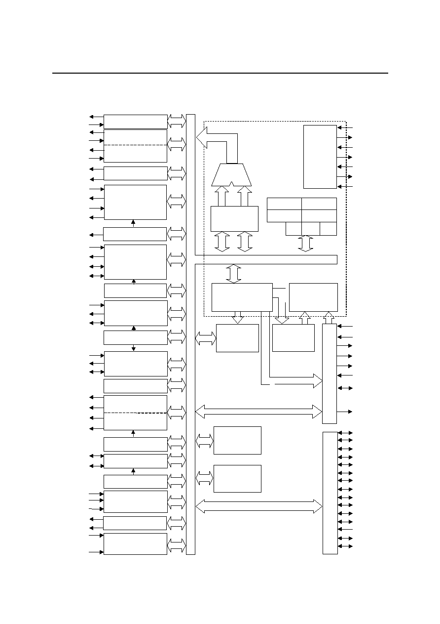
BLOCK DIAGRAM
*: Address output/data I/O when
selecting multiplexed bus type.
NMI
EXINT0
to
EXINT7
TM4OUT
SIOI4
SIOO4
SIOCK4
PWMOUT0
PWMOUT2
PWMOUT1
PWMOUT3
CPCM0
CPCM1
SIOI5
SIOO5
SIOCK5
AO0
AO1
Instruction
Decoder
RAM
4K/12K
TBC
RTC
TM0OUT
TM0EVT
TM1OUT
TM1EVT
TM2OUT
TM2EVT
CLKOUT
XTOUT
CPU Core
Port C
ontr
o
l
ROM
128K
Bus
Port
Contro
l
RXD1
TXD1
RXC1
TXC1
16 bit Timer0
Peripheral
SIO1
(UART/SYNC)
8 bit Time4/BRG
8 bit PWM0
8 bit PWM1
SIO4
(32 byte FIFO SYNC)
8 bit Timer3/BRG
8 bit Timer6/WDT
8 bit Timer9
CAP/CMP
16 bit FRC
10 bit A/D
Converter
Interrupt
V
REF
AGND
AI0
to
AI7
ALU Control
ACC
P0
P1
P2
P3
P4
P5
P6
P7
P8
P9
P10
P11
P12
P14
P15
System
Control
Memory Control
Pointing Registers
SSP
LRB
PSW
PC
DSR TSR CSR
Control
Registers
ALU
EA
SELMBUS
PSEN
RD
WR
WAIT
D0 to D7
A0 to A19
XT0
XT1
OSC0
OSC1
HOLD
HLDACK
RES
8 bit Timer1
8 bit Timer2
RXD6
TXD6
RXC6
TXC6
SIO6
(UART/SYNC)
SIO5
(32 byte FIFO SYNC)
8 bit D/A Converter
(AD0 to AD7*)
8 bit Timer5/BRG
(AD8 to AD19*)
PEDL66579-03
1Semiconductor
MSM66579 Family
6/37
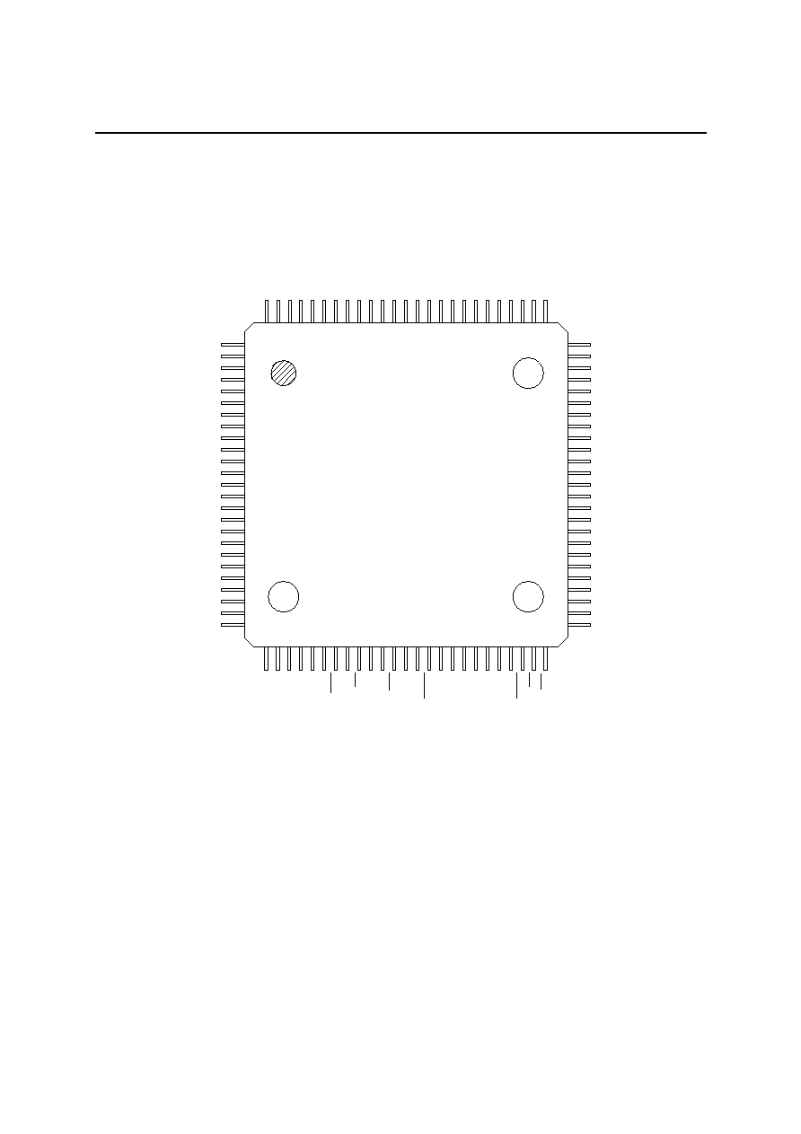
PIN CONFIGURATION (TOP VIEW)
SIOCK4/P10-3
SIOO4/P10-4
SIOI4/P10-5
RXD1/P8-0
TXD1/P8-1
RXC1/P8-2
TXC1/P8-3
TM4OUT/P8-4
PWM2OUT/P8-6
PWM3OUT/P8-7
PWM0OUT/P7-6
PWM1OUT/P7-7
V
DD
GND
HLDACK/P9-7
EXINT4/P9-0
EXINT5/P9-1
EXINT6/P9-2
EXINT7/P9-3
EXINT0/P6-0
EXINT1/P6-1
EXINT2/P6-2
EXINT3/P6-3
TM1EVT/P6-4
TM1OUT/P6-5
P1-6/A14
P1-5/A13
P1-4/A12
P1-3/A11
P1-2/A10
P1-1/A9
P1-0/A8
P4-7/A7
P4-6/A6
P4-5/A5
P4-4/A4
P4-3/A3
P4-2/A2
P4-1/A1
P4-0/A0
GND
P0-7/D7(AD7*)
P0-6/D6(AD6*)
P0-5/D5(AD5*)
P0-4/D4(AD4*)
P0-3/D3(AD3*)
P0-2/D2(AD2*)
P0-1/D1(AD1*)
P0-0/D0(AD0*)
P3-3/WR
P3-2/RD
P3-1/PSEN
P3-0/ALE
SELMBUS
P11-3/XTOUT
P11-2/CLKOUT
P11-1/HOLD
P11-0/WAIT
V
DD
OSC1
OSC0
GND
XT1
XT0
V
DD
EA
NMI
RES
P5-7/TM0EVT
P5-6/TM0OUT
P5-5/CPCM1
P5-4/CPCM0
P6-7/TM2OUT
P6-6/TM2EVT
A16/P2-0
A17/P2-1
A18/P2-2
A19/P2-3
V
DD
V
REF
AI0/P12-0
AI1/P12-1
AI2/P12-2
AI3/P12-3
AI4/P12-4
AI5/P12-5
AI6/P12-6
AI7/P12-7
AGND
AO1/P14-7
AO0/P14-6
GND
SIOI5/14-2
SIOO5/P14-1
SIOCK5/P14-0
RXD6/P15-0
TXD6/P15-1
RXC6/P15-2
TXC6/P15-3
80
85
90
95
100
1
5
10
15
20
25
75
70
65
60
55
50
45
40
35
30
P1-7/A15
100-pin Plastic TQFP
*: Address output/data I/O when selecting multiplexed bus type.
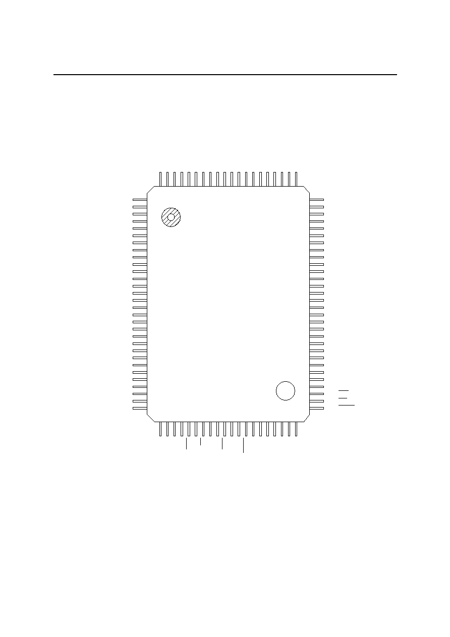
PEDL66579-03
1Semiconductor
MSM66579 Family
7/37
SIOCK4/P10-3
SIOO4/P10-4
SIOI4/P10-5
RXD1/P8-0
TXD1/P8-1
RXC1/P8-2
TXC1/P8-3
TM4OUT/P8-4
PWM2OUT/P8-6
PWM3OUT/P8-7
PWM0OUT/P7-6
PWM1OUT/P7-7
V
DD
GND
HLDACK/P9-7
EXINT4/P9-0
EXINT5/P9-1
EXINT6/P9-2
EXINT7/P9-3
EXINT0/P6-0
EXINT1/P6-1
EXINT2/P6-2
EXINT3/P6-3
TM2EVT/P6-6
TM1EVT/P6-4
TM1OUT/P6-5
P1-6/A14
P1-5/A13
P1-4/A12
P1-3/A11
P1-2/A10
P1-1/A9
P1-0/A8
P4-7/A7
P4-6/A6
P4-5/A5
P4-4/A4
P4-3/A3
P4-2/A2
P4-1/A1
P4-0/A0
GND
P0-7/D7(AD7*)
P0-6/D6(AD6*)
P0-5/D5(AD5*)
P0-4/D4(AD4*)
P0-3/D3(AD3*)
P0-2/D2(AD2*)
P0-1/D1(AD1*)
P0-0/D0(AD0*)
P3-3/WR
P3-2/RD
P3-1/PSEN
P3-0/ALE
SELMBUS
P11-3/XTOUT
P11-2/CLKOUT
P11-1/HOLD
P11-0/WAIT
V
DD
OSC1
OSC0
GND
XT1
XT0
V
DD
EA
NMI
RES
P5-7/TM0EVT
P5-6/TM0OUT
P5-5/CPCM1
P5-4/CPCM0
A18/P2-2
A19/P2-3
V
DD
V
REF
AI0/P12-0
AI1/P12-1
AI2/P12-2
AI3/P12-3
AI4/P12-4
AI5/P12-5
AI6/P12-6
AI7/P12-7
AGND
AO1/P14-7
AO0/P14-6
GND
SIOI5/P14-2
SIOO5/P14-1
SIOCK5/P14-0
RXD6/P15-0
TXD6/P15-1
RXC6/P15-2
TXC6/P15-3
85
90
95
100
1
5
10
15
20
25
TM2OUT/P6-7
30
80
75
70
65
60
55
50
45
40
35
P1-7/A15
P2-0/A16
P2-1/A17
100-pin Plastic QFP
*: Address output/data I/O when selecting multiplexed bus type.
PEDL66579-03
1Semiconductor
MSM66579 Family
8/37
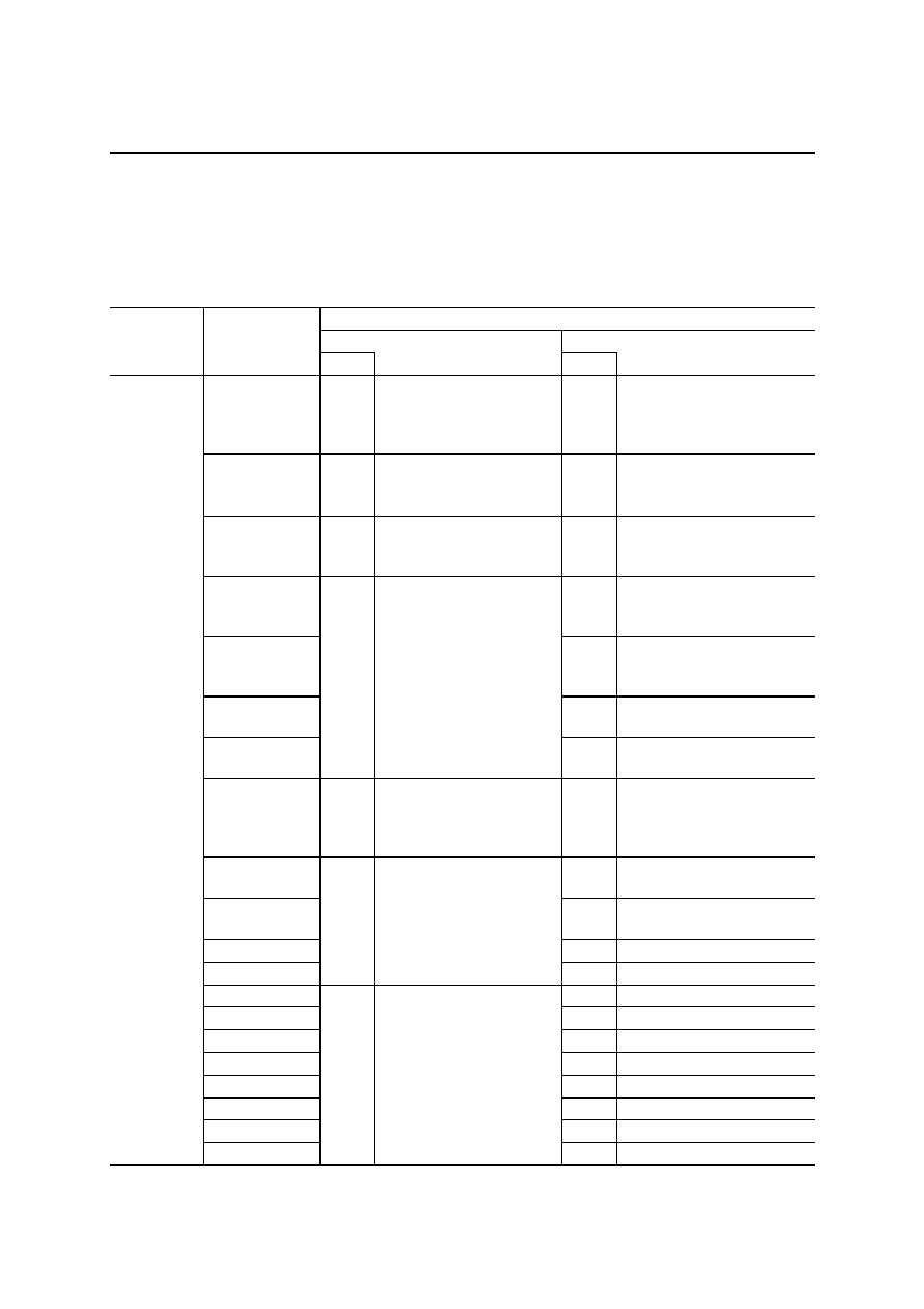
PIN DESCRIPTIONS
In the Type column, "I" indicates an input pin, "O" indicates an output pin, and "I/O" indicates an I/O pin.
Description
Function
Symbol
Type
Primary function
Type
Secondary function
P0_0/D0 (AD0)
to
P0_7/D7 (AD7)
I/O
8-bit I/O port
10 mA sink capability
Pull-up resistors can be
specified for each individual bit
I/O
External memory access
Data I/O port
(Address output/data I/O port when
selecting a multiplexed bus)
P1_0/A8
to
P1_7/A15
I/O
8-bit I/O port
Pull-up resistors can be
specified for each individual bit
O
External memory access
Address output port
P2_0/A16
to
P2_3/A19
I/O
4-bit I/O port
Pull-up resistors can be
specified for each individual bit
O
External memory access
Address output port
P3_0/ALE
O
External memory access
Address latch enable signal
output pin
P3_1/PSEN
O
External program memory
access
Read strobe output pin
P3_2/RD
O
External memory access
Read strobe output pin
P3_3/WR
I/O
4-bit I/O port
10 mA sink capability
Pull-up resistors can be
specified for each individual bit
O
External memory access
Write strobe output pin
P4_0/A0
to
P4_7/A7
I/O
8-bit I/O port
Pull-up resistors can be
specified for each individual bit
O
External memory access
Address output port
(When selecting a separate bus
type)
P5_4/CPCM0
I/O
Capture 0 input / Compare
0 output pin
P5_5/CPCM1
I/O
Capture 1 input / Compare
1 output pin
P5_6/TM0OUT
O
Timer 0 timer output pin
P5_7/TM0EVT
I/O
4-bit I/O port
Pull-up resistors can be
specified for each individual bit
I
Timer 0 external event input pin
P6_0/EXINT0
I
External interrupt 0 input pin
P6_1/EXINT1
I
External interrupt 1 input pin
P6_2/EXINT2
I
External interrupt 2 input pin
P6_3/EXINT3
I
External interrupt 3 input pin
P6_4/TM1EVT
I
Timer1 external event input pin
P6_5/TM1OUT
O
Timer 1 timer output pin
P6_6/TM2EVT
I
Timer 2 external event pin
Port
P6_7/TM2OUT
I/O
8-bit I/O port
Pull-up resistors can be
specified for each individual bit
O
Timer 2 timer output pin
PEDL66579-03
1Semiconductor
MSM66579 Family
9/37
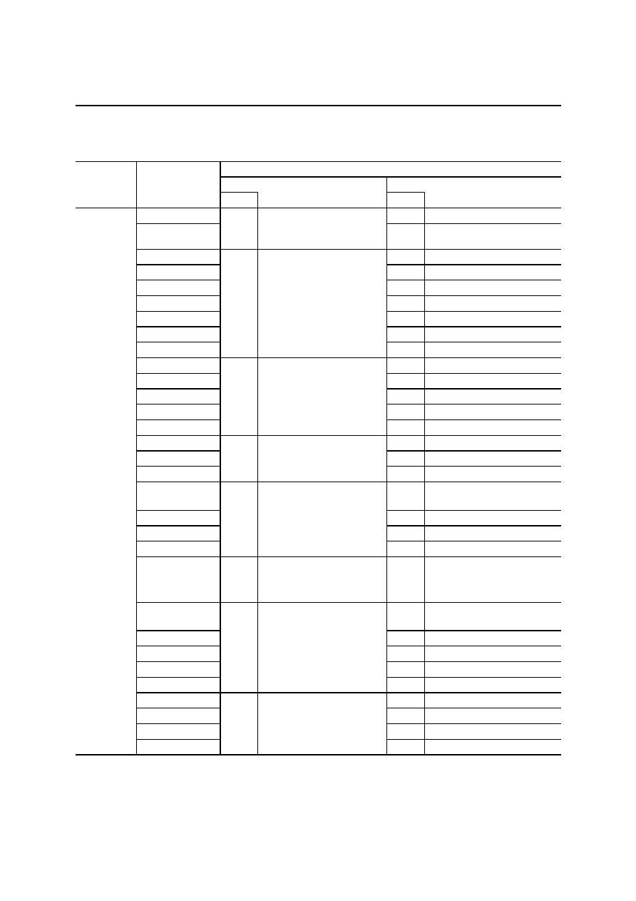
Description
Function
Symbol
Type
Primary function
Type
Secondary function
P7_6/PWM0OUT
O
PWM0 output pin
P7_7/PWM1OUT
I/O
2-bit I/O port
Pull-up resistors can be
specified for each individual bit
O
PWM1 output pin
P8_0/RXD1
I
SIO1 receive data input pin
P8_1/TXD1
O
SIO1 transmit data output pin
P8_2/RXC1
I/O
SIO1 receive clock I/O pin
P8_3/TXC1
I/O
SIO1 transmit clock I/O pin
P8_4/TM4OUT
O
Timer 4 timer output pin
P8_6/PWM2OUT
O
PWM2 output pin
P8_7/PWM3OUT
I/O
7-bit I/O port
Pull-up resistors can be
specified for each individual bit
O
PWM3 output pin
P9_0/EXINT4
I
External Interrupt 4 input pin
P9_1/EXINT5
I
External Interrupt 5 input pin
P9_2/EXINT6
I
External Interrupt 6 input pin
P9_3/EXINT7
I
External Interrupt 7 input pin
P9_7/HLDACK
I/O
5-bit I/O port
Pull-up resistors can be
specified for each individual bit
O
HOLD mode output pin
P10_3/SIOCK4
I/O
SIO4 transmit-receive clock I/O pin
P10_4/SIOO4
I
SIO4 receive data input pin
P10_5/SIOI4
I/O
3-bit I/O port
Pull-up resistors can be
specified for each individual bit
O
SIO4 transmit data output pin
P11_0/WAIT
I
External data memory access
wait input pin
P11_1/HOLD
I
HOLD mode request input pin
P11_2/CLKOUT
O
Main clock pulse output pin
P11_3/XTOUT
I/O
4-bit I/O port
10 mA sink capability
Pull-up resistors can be
specified for each individual bit
O
Sub clock pulse output pin
P12_0/AI0
to
P12_7/AI7
I
8-bit input port
I
A/D converter analog input port
P14_0/SIOCK5
I/O
SIO5 transmit-receive clock I/O
pin
P14_1/SIOO5
O
SIO5 transmit data output pin
P14_2/SIOI5
I
SIO5 receive data input pin
P14_6/AO0
O
D/A converter analog output port
P14_7/AO1
I/O
5-bit I/O port
Pull-up resistors can be
specified for each individual bit
O
D/A converter analog output port
P15_0/RXD6
I
SIO6 receive data input pin
P15_1/TXD6
O
SIO6 transmit data output pin
P15_2/RXC6
I/O
SIO6 receive clock I/O pin
Port
P15_3/TXC6
I/O
4-bit I/O port
Pull-up resistors can be
specified for each individual bit
I/O
SIO6 transmit clock I/O pin
PEDL66579-03
1Semiconductor
MSM66579 Family
10/37
Function
Symbol
Type
Description
V
DD
I
Power supply pin
Connect all V
DD
pins to the power supply.*
GND
I
GND pin
Connect all GND pins to GND.*
V
REF
I
Analog reference voltage pin
Power
supply
AGND
I
Analog GND pin
XT0
I
Sub clock oscillation input pin
Connect to a crystal oscillator of f = 32.768 kHz.
XT1
O
Sub clock oscillation output pin
Connect to a crystal oscillator of f = 32.768 kHz.
The clock output is opposite in phase to XT0.
OSC0
I
Main clock oscillation input pin
Connect to a crystal or ceramic oscillator. Or, input an external
clock.
Oscillation
OSC1
O
Main clock oscillation output pin
Connect to a crystal or ceramic oscillator.
The clock output is opposite in phase to OSC0.
Leave this pin unconnected when an external clock is used.
Reset
RES
I
Reset input pin
NMI
I
Non-maskable interrupt input pin
EA
I
External program memory access input pin
If the EA pin is enabled (low level), the internal program memory is
masked and the CPU executes the program code in external
program memory through all address space.
Other
SELMBUS
I
SELMBUS = H: Address/data separate bus type
SELMBUS = L: Multiplexed bus type
* Each of the family devices has unique pattern routes for the internal power and ground. Connect the
power supply voltage to all V
DD
pins and the ground potential to all GND pins. If a device may have one
or more V
DD
or GND pins to which the power supply voltage or the ground potential is not connected, it
can not be guaranteed for normal operation.
PEDL66579-03
1Semiconductor
MSM66579 Family
11/37
ABSOLUTE MAXIMUM RATINGS
Parameter
Symbol
Condition
Rating
Unit
Digital power supply voltage
V
DD
�0.3 to +7.0
V
Input voltage
V
I
�0.3 to V
DD
+ 0.3
V
Output voltage
V
O
�0.3 to V
DD
+ 0.3
V
Analog reference voltage
V
REF
�0.3 to V
DD
+ 0.3
V
Analog input voltage
V
AI
GND = AGND = 0 V
Ta = 25�C
�0.3 to V
REF
V
100-pin TQFP
650
mW
Power dissipation
P
D
Ta = 70�C
per package 100-pin QFP
750
mW
Storage Temperature
T
STG
--
�50 to +150
�C
RECOMMENDED OPERATING CONDITIONS
Parameter
Symbol
Condition
Range
Unit
MSM66577
f
OSC
30 MHz
4.5 to 5.5
MSM66577L
f
OSC
14 MHz
2.4 to 3.6
MSM66579L
f
OSC
28 MHz
2.4 to 3.6
MSM66Q577
f
OSC
30 MHz
4.5 to 5.5
MSM66Q577L
f
OSC
14 MHz
2.7 to 3.3
Digital power supply voltage
V
DD
MSM66Q579L
f
OSC
28 MHz
2.7 to 3.3
V
Analog reference voltage
V
REF
--
V
DD
�0.3 to V
DD
V
Analog input voltage
V
AI
--
AGND to V
REF
V
Memory hold voltage
V
DDH
f
OSC
= 0 Hz
2.0 to 5.5
V
MSM66577
V
DD
= 4.5 to 5.5 V
2 to 30
MSM66577L
V
DD
= 2.4 to 3.6 V
2 to 14
MSM66579L
V
DD
= 2.4 to 3.6 V
2 to 28
MSM66Q577
V
DD
= 4.5 to 5.5 V
2 to 30
MSM66Q577L
V
DD
= 2.7 to 3.3 V
2 to 14
f
OSC
MSM66Q579L
V
DD
= 2.7 to 3.3 V
2 to 28
MHz
Operating frequency
f
XT
--
32.768
kHz
Ambient temperature
Ta
--
�30 to +70
�C
MOS load
20
--
P0, P3, P11
6
--
Fan out
N
TTL load
P1, P2, P4, P5, P6,
P7, P8, P9, P10,
P14, P15
1
--
PEDL66579-03
1Semiconductor
MSM66579 Family
12/37
ALLOWABLE OUTPUT CURRENT VALUES
MSM66577L/577/579L (V
DD
= 2.4 to 3.6 V/4.5 to 5.5 V, Ta = �30 to +70�C)
MSM66Q577L/Q577/Q579L (V
DD
= 2.7 to 3.3 V/4.5 to 5.5 V, Ta = �30 to +70�C)
Parameter
Pin
Symbol
Min.
Typ.
Max.
Unit
"H" output pin (1 pin)
All output pins
I
OH
--
--
�2
"H" output pins (sum total)
Sum total of all output pins
I
OH
--
--
�40
P0, P3, P11
10
"L" output pin (1 pin)
Other ports
I
OL
--
--
5
Sum total of P0, P3, P11
80
Sum total of P1, P2, P4
Sum total of P5, P6, P9
Sum total of P7, P8, P10,
P14, P15
50
"L" output pins (sum total)
Sum total of all output pins
I
OL
--
--
140
mA
[Note]
Each of the family devices has unique pattern routes for the internal power and ground. Connect the
power supply voltage to all V
DD
pins and the ground potential to all GND pins. If a device may have one
or more V
DD
or GND pins to which the power supply voltage or the ground potential is not connected, it
can not be guaranteed for normal operation.
PEDL66579-03
1Semiconductor
MSM66579 Family
13/37
ELELCTRICAL CHARACTERISTICS
DC Characteristics 1 (V
DD
= 4.5 to 5.5 V)
(V
DD
= 4.5 to 5.5 V, Ta = �30 to +70�C)
Parameter
Symbol
Condition
Min.
Typ.
Max.
Unit
"H" input voltage
*1
0.44V
DD
--
V
DD
+0.3
"H" input voltage
*2,*3,*4,*5,*6,*7
V
IH
--
0.80V
DD
--
V
DD
+0.3
"L" input voltage
*1
�0.3
--
0.16V
DD
"L" input voltage
*2,*3,*4,*5,*6,*7
V
IL
--
�0.3
--
0.2V
DD
I
O
= �400 �A
V
DD
�0.4
--
--
"H" output voltage *1, *4
I
O
= �2.0 mA
V
DD
�0.6
--
--
I
O
= �200 �A
V
DD
�0.4
--
--
"H" output voltage *2
V
OH
I
O
= �2.0 mA
V
DD
�0.6
--
--
I
O
= 3.2 mA
--
--
0.4
"L" output voltage *1, *4
I
O
= 10.0 mA
--
--
0.8
I
O
= 1.6 mA
--
--
0.4
"L" output voltage *2
V
OL
I
O
= 5.0 mA
--
--
0.8
V
Input leakage current *3, *6
--
--
1/�1
Input current *5
--
--
1/�250
Input current *7
I
IH
/I
IL
V
I
= V
DD
/0 V
--
--
15/�15
�A
Output leakage current *1, *2, *4
I
LO
V
O
= V
DD
/0 V
--
--
�10
�A
Pull-up resistance
R
pull
V
I
= 0 V
25
50
100
k
Input capacitance
C
I
--
5
--
Output capacitance
C
O
f = 1 MHz, Ta = 25�C
--
7
--
pF
During A/D operation
--
--
4
mA
Analog reference supply current
I
REF
When A/D is stopped
--
--
10
�A
OSC is stopped,
XT is not used.
V
DD
= 2 V, Ta = 25�C *8
--
0.2
10
Supply current
(STOP mode)
I
DDS
OSC is stopped,
XT is not used. *8
--
1
100
�A
f = 30 MHz, No Load
--
40
60
mA
Supply current
(HALT mode)
I
DDH
f = 30 MHz, No Load
--
60
90
mA
Supply current
I
DD
f = 32.768 kHz, No Load
--
70
120
�A
*1: Applicable to P0
*5: Applicable to
RES
*2: Applicable to P1, P2, P4, P5, P6, P7, P8, P9,
*6: Applicable to SELMBUS,
EA, NMI
P10, P14, P15
*7: Applicable to OSC0
*3: Applicable to P12
*8: Ports used as inputs are at V
DD
or 0 V.
*4: Applicable to P3, p11
Other ports are unloaded.
PEDL66579-03
1Semiconductor
MSM66579 Family
14/37
DC Characteristics 2 (V
DD
= 2.4 to 3.6 V)
MSM66577L/579L (V
DD
= 2.4 to 3.6 V, Ta = �30 to +70�C)
MSM66Q577L/Q579L (V
DD
= 2.7 to 3.3 V, Ta = �30 to +70�C)
Parameter
Symbol
Condition
Min.
Typ.
Max.
Unit
"H" input voltage
*1
0.44V
DD
--
V
DD
+0.3
"H" input voltage
*2,*3,*4,*5,*6,*7
V
IH
--
0.80V
DD
--
V
DD
+0.3
"L" input voltage
*1
�0.3
--
0.16V
DD
"L" input voltage
*2,*3,*4,*5,*6,*7
V
IL
--
�0.3
--
0.2V
DD
I
O
= �400 �A
V
DD
�0.4
--
--
"H" output voltage *1, *4
I
O
= �2.0 mA
V
DD
�0.8
--
--
I
O
= �200 �A
V
DD
�0.4
--
--
"H" output voltage *2
V
OH
I
O
= �1.0 mA
V
DD
�0.8
--
--
I
O
= 3.2 mA
--
--
0.5
"L" output voltage *1, *4
I
O
= 5.0 mA
--
--
0.9
I
O
= 1.6 mA
--
--
0.5
"L" output voltage *2
V
OL
I
O
= 2.5 mA
--
--
0.9
V
Input leakage current *3, *6
--
--
1/�1
Input current *5
--
--
1/�250
Input current *7
I
IH
/I
IL
V
I
= V
DD
/0 V
--
--
15/�15
�A
Output leakage current *1, *2, *4
I
LO
V
O
= V
DD
/0 V
--
--
�10
�A
Pull-up resistance
R
pull
V
I
= 0 V
40
100
200
k
Input capacitance
C
I
--
5
--
Output capacitance
C
O
f = 1 MHz, Ta = 25�C
--
7
--
pF
During A/D operation
--
--
2
mA
Analog reference supply current
I
REF
When A/D is stopped
--
--
5
�A
OSC is stopped,
XT is not used.
V
DD
= 2 V, Ta = 25�C *8
--
0.2
10
Supply current
(STOP mode)
I
DDS
OSC is stopped,
XT is not used. *8
--
1
100
�A
f = 14 MHz, No Load
--
--
TBD
mA
Supply current
(HALT mode)
I
DDH
f = 14 MHz, No Load
--
--
TBD
mA
Supply current
I
DD
f = 32.768 kHz, No Load
--
--
TBD
�A
*1: Applicable to P0
*5: Applicable to
RES
*2: Applicable to P1, P2, P4, P5, P6, P7, P8, P9,
*6: Applicable to SELMBUS,
EA, NMI
P10, P14, P15
*7: Applicable to OSC0
*3: Applicable to P12
*8: Ports used as inputs are at V
DD
or 0 V.
*4: Applicable to P3, p11
Other ports are unloaded.
PEDL66579-03
1Semiconductor
MSM66579 Family
15/37
AC Characteristics 1 (V
DD
= 4.5 to 5.5 V)
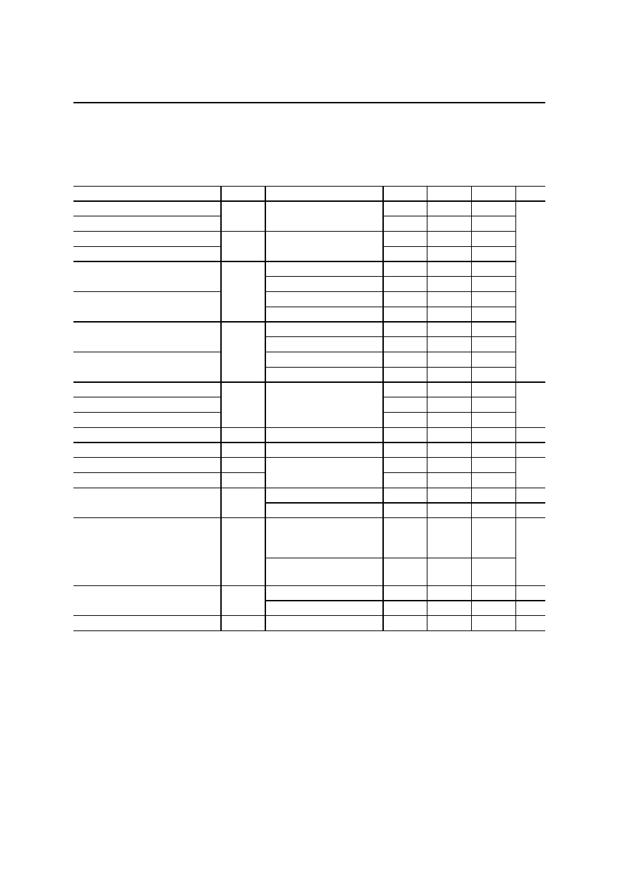
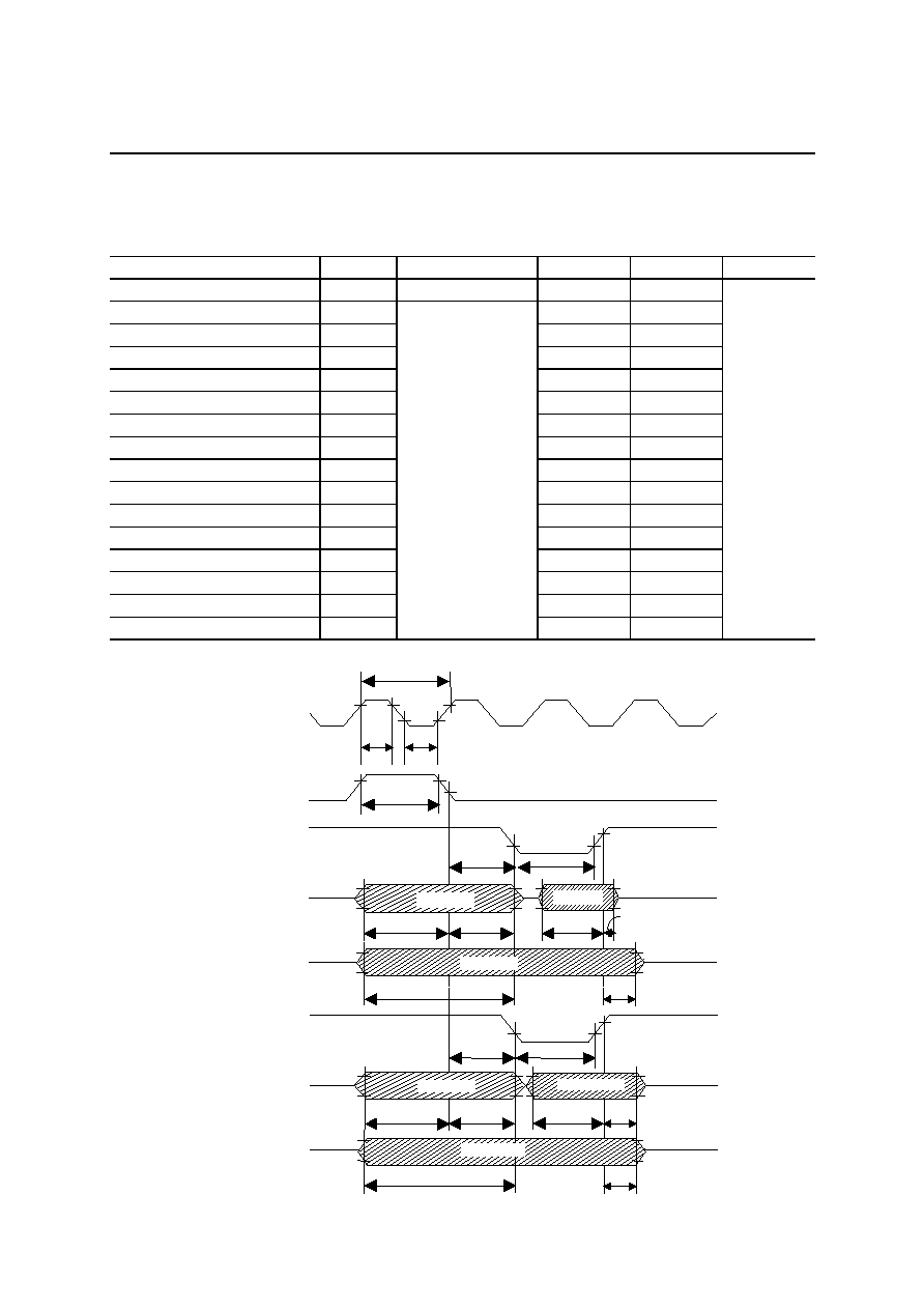
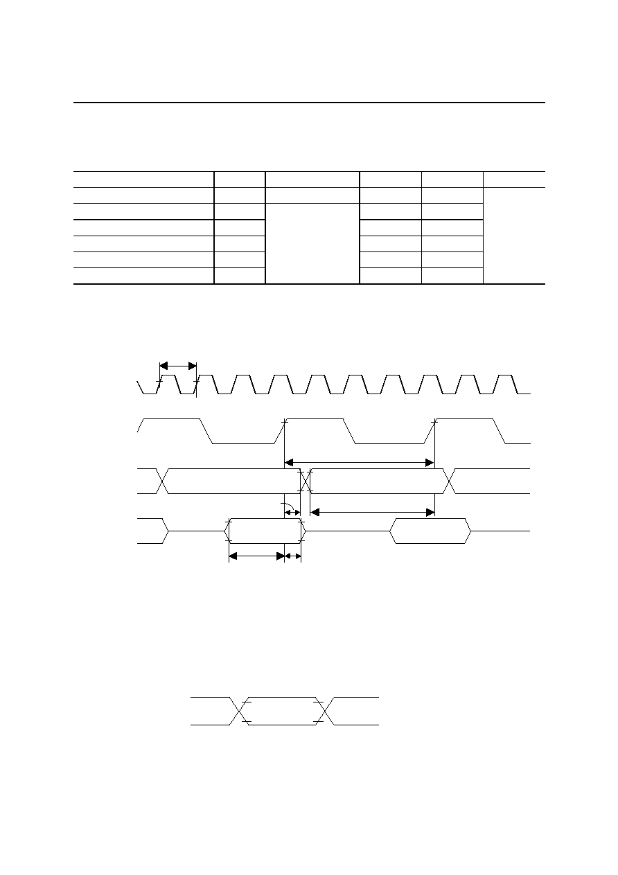
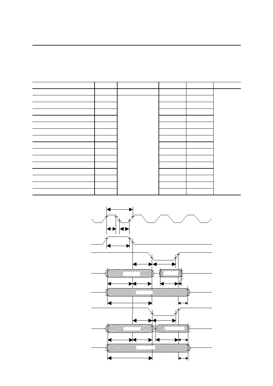
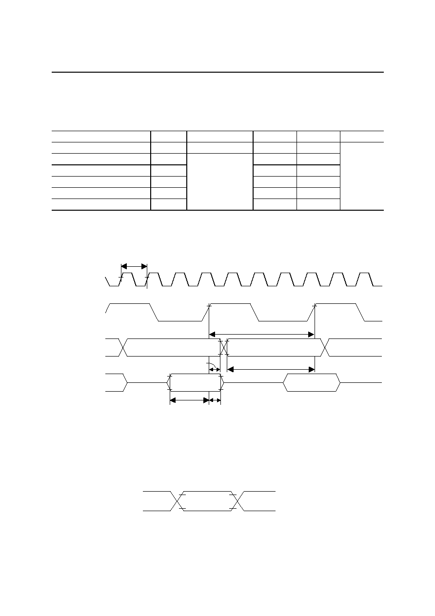
(1) Separate Bus Type
External program memory control
(V
DD
= 4.5 to 5.5 V, Ta = �30 to +70�C)
Parameter
Symbol
Condition
Min.
Max.
Unit
Cycle time
t
cyc
f
OSC
= 30 MHz
33.3
--
Clock pulse width (HIGH level)
t
WH
13
--
Clock pulse width (LOW level)
t
WL
13
--
PSEN pulse width
t
PW
2 t
� 15
--
PSEN pulse delay time
t
PD
--
45
Address setup time
t
AS
t
� 25
--
Address hold time
t
AH
0
9
Instruction setup time
t
IS
30
--
Instruction hold time
t
IH
0
--
Read data access time
t
ACC
C
L
= 50 pF
--
3 t
� 70
ns
Note: t
= t
cyc
/2
INST0 to 7
PC0 to 19
Bus timing during no wait cycle time
t
cyc
t
WH
CPUCLK
PSEN
A0 to A19
D0 to D7
t
WL
t
PD
t
PW
t
AS
t
ACC
t
IS
t
IH
t
AH
PEDL66579-03
1Semiconductor
MSM66579 Family
16/37
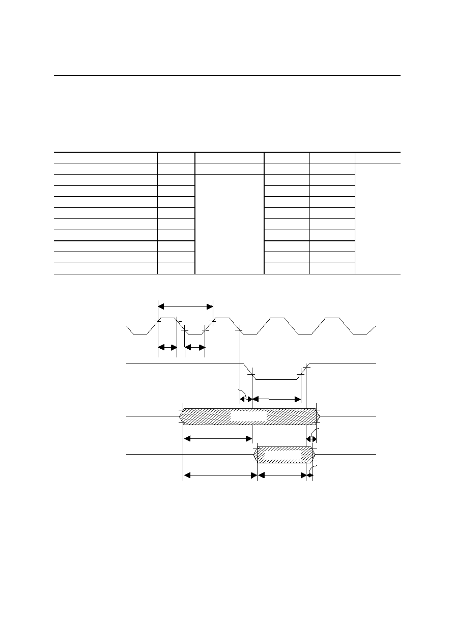
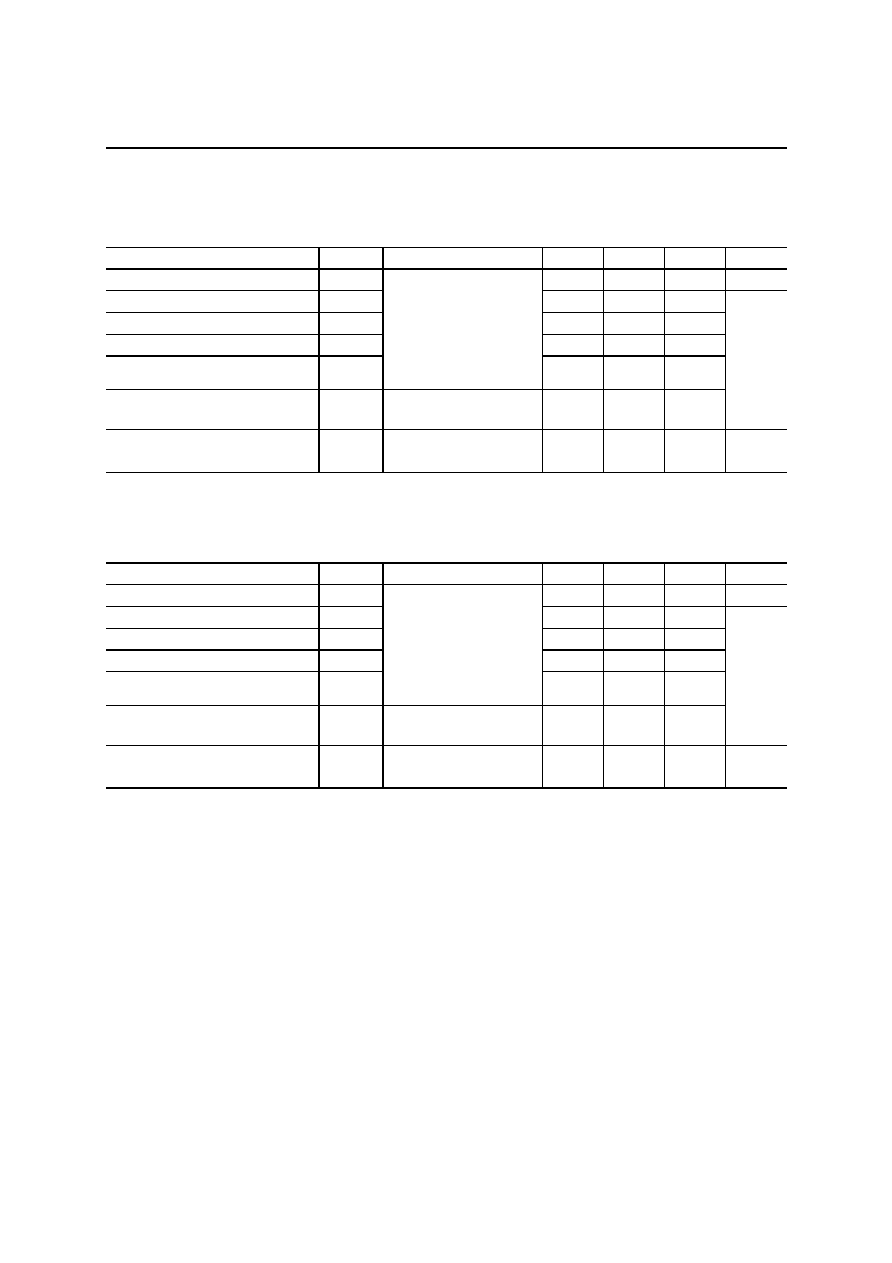
External data memory control
(V
DD
= 4.5 to 5.5 V, Ta = �30 to +70�C)
Parameter
Symbol
Condition
Min.
Max.
Unit
Cycle time
t
cyc
f
OSC
= 30 MHz
33.3
--
Clock pulse width (HIGH level)
t
WH
13
--
Clock pulse width (LOW level)
t
WL
13
--
RD pulse width
t
RW
2 t
� 15
--
WR pulse width
t
WW
2 t
� 15
--
RD pulse delay time
t
RD
--
45
WR pulse delay time
t
WD
--
45
Address setup time
t
AS
t
� 25
--
Address hold time
t
AH
t
� 3
t
+3
Read data setup time
t
RS
30
--
Read data hold time
t
RH
0
--
Read data access time
t
ACC
--
3t
�70
Write data setup time
t
WS
2t
� 30
--
Write data hold time
t
WH
C
L
= 50 pF
t
� 3
t
+ 3
ns
Note: t
= t
cyc
/2
DIN0 to 7
RAP0 to 19
t
RD
t
cyc
t
WH
CPUCLK
RD
A0 to A19
D0 to D7
DOUT0 to 7
RAP0 to 19
Bus timing during no wait cycle time
WR
A0 to A19
D0 to D7
t
WL
t
RW
t
AS
t
ACC
t
RS
t
WW
t
WD
t
AH
t
RH
t
AH
t
AS
t
WS
t
WH
PEDL66579-03
1Semiconductor
MSM66579 Family
17/37
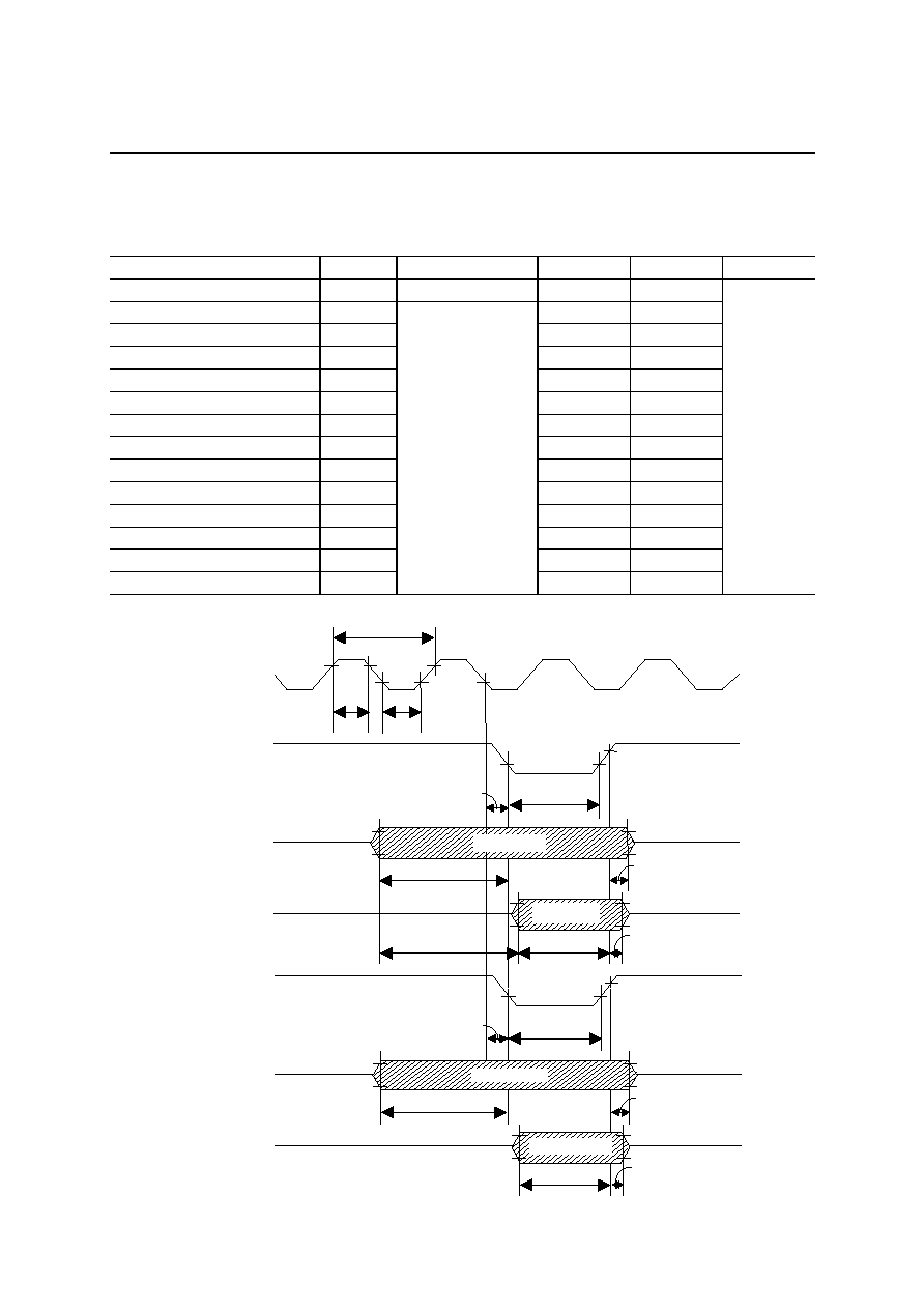
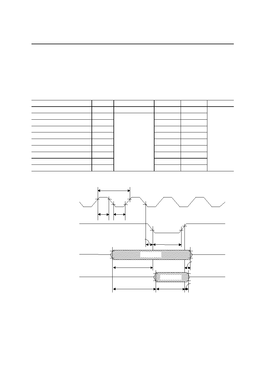
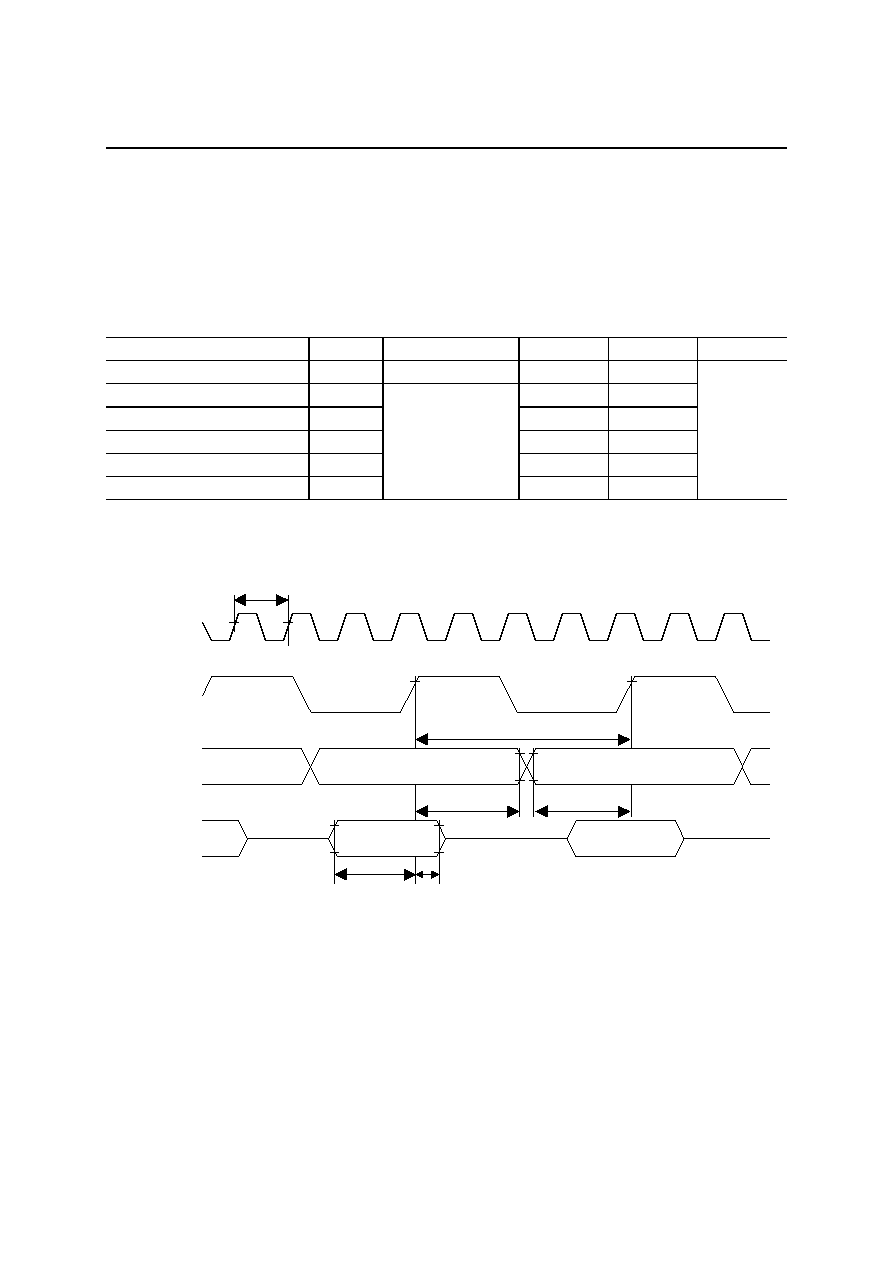
(2) Multiplexed bus type
External program memory control
(V
DD
= 4.5 to 5.5 V, Ta = �30 to +70�C)
Parameter
Symbol
Condition
Min.
Max.
Unit
Cycle time
t
cyc
f
OSC
= 30 MHz
33.3
--
Clock pulse width (HIGH level)
t
WH
13
--
Clock pulse width (LOW level)
t
WL
13
--
ALE pulse width
T
AW
2 t
� 10
--
PSEN pulse width
t
PW
2 t
� 14
--
PSEN pulse delay time
t
PAD
t
� 10
t
+ 10
Low address setup time
t
ALS
2t
� 20
2t
+ 3
Low address hold time
t
ALH
t
� 10
t
+ 10
High address setup time
t
AHS
3t
� 30
4t
+ 3
High address hold time
t
AHH
0
t
+ 10
Instruction setup time
t
IS
24
--
Instruction hold time
t
IH
C
L
= 50 pF
0
t
� 3
ns
Note: t
= t
cyc
/2
t
cyc
INST0 to 7
t
WH
CPUCLK
PSEN
A8 to A19
AD0 to AD7
ALE
PC0 to 7
PC8 to 19
t
WL
t
AW
t
PAD
t
PW
t
ALS
t
ALH
t
IS
t
IH
t
AHS
t
AHH
Bus timing during no wait cycle time
PEDL66579-03
1Semiconductor
MSM66579 Family
18/37
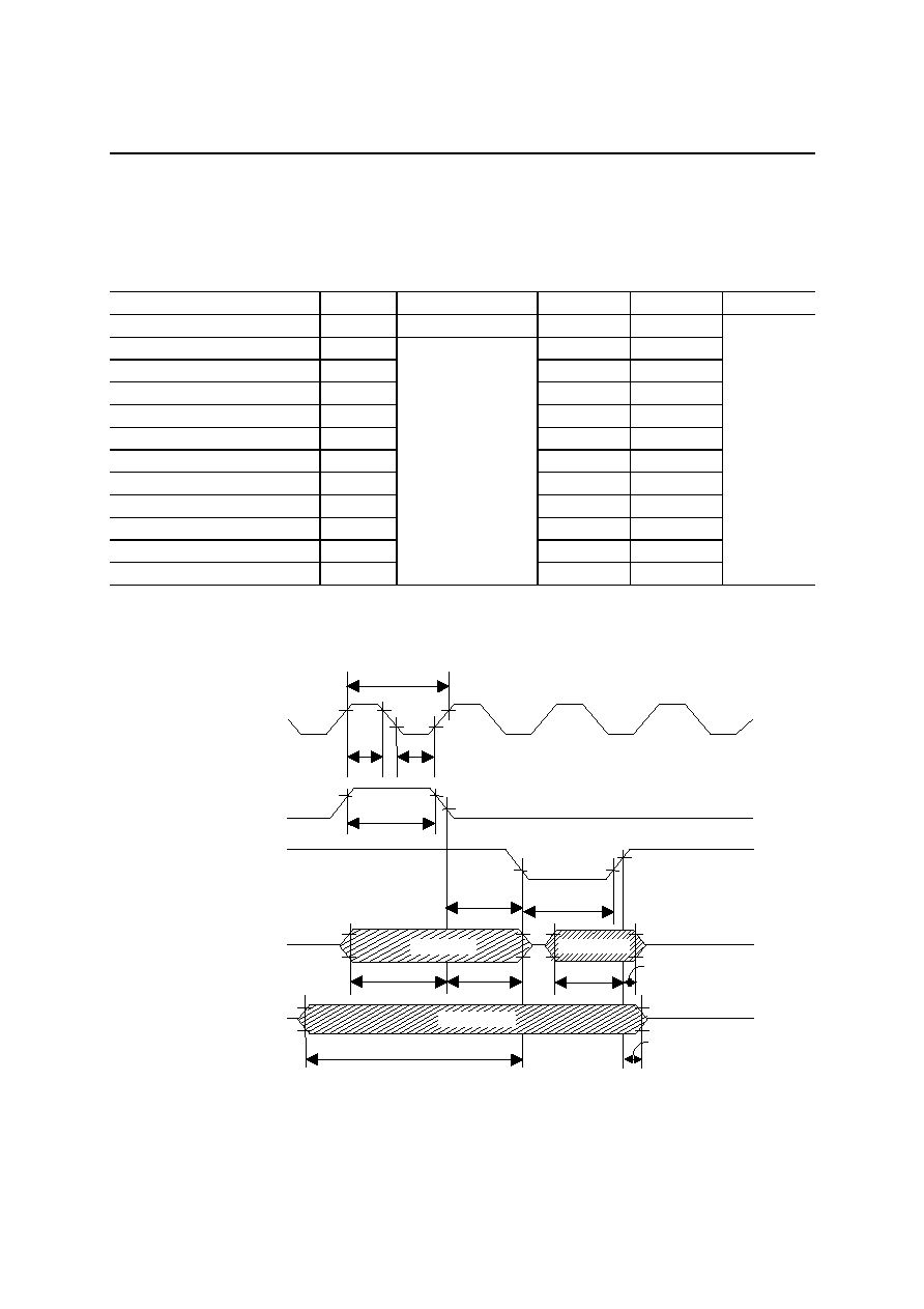
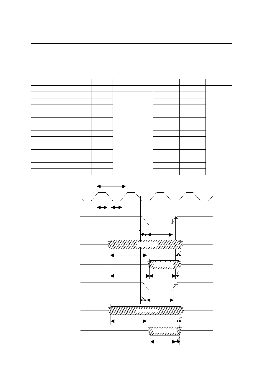
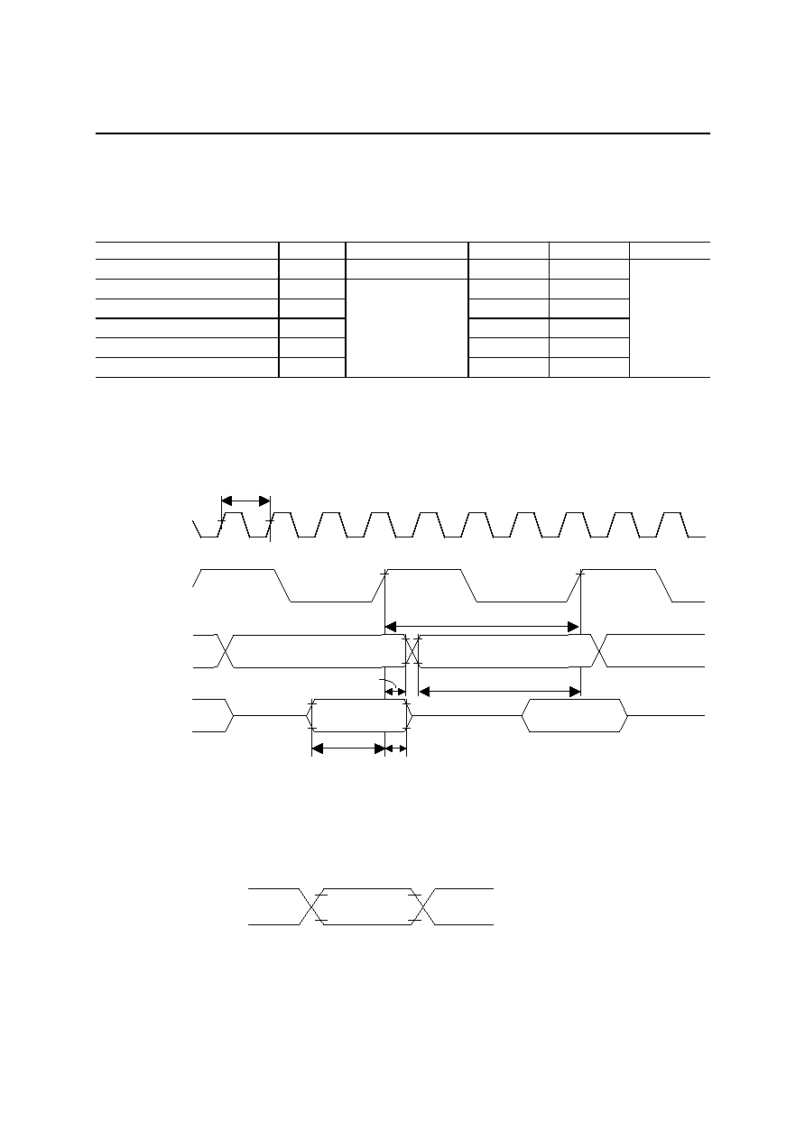
External data memory control
(V
DD
= 4.5 to 5.5 V, Ta = �30 to +70�C)
Parameter
Symbol
Condition
Min.
Max.
Unit
Cycle time
t
cyc
f
OSC
= 30 MHz
33.3
--
Clock pulse width (HIGH level)
t
WH
13
--
Clock pulse width (LOW level)
t
WL
13
--
ALE pulse width
t
AW
2 t
� 10
--
RD pulse width
t
RW
2 t
� 14
--
WR pulse width
t
WW
2 t
� 14
--
RD pulse delay time
t
RAD
t
� 10
t
+10
WR pulse delay time
t
WAD
t
� 10
t
+10
Low address setup time
t
ALS
2 t
� 20
2 t
+3
Low address hold time
t
ALH
t
� 10
t
+10
High address setup time
t
AHS
3 t
� 30
3 t
+3
High address hold time
t
AHH
t
� 10
t
+10
Read data setup time
t
RS
24
--
Read data hold time
t
RH
0
t
� 3
Write data setup time
t
WS
2t
� 12
--
Write data hold time
t
WH
C
L
= 50 pF
t
� 3
t
+ 3
ns
Note: t
= t
cyc
/2
DIN0 to 7
RAP8 to 19
A
t
cyc
t
WH
CPUCLK
RD
A8 to A19
AD0 to AD7
ALE
RAP0 to 7
DOUT0 to 7
WR
A8 to A19
AD0 to AD7
RAP0 to 7
Bus timing during no wait cycle time
RAP8 to 19
t
WL
t
AW
t
RAD
t
RW
t
ALS
t
ALH
t
RS
t
RH
t
AHH
t
AHS
t
WAD
t
WW
t
WH
t
WS
t
ALS
t
ALH
t
AHH
t
AHS
PEDL66579-03
1Semiconductor
MSM66579 Family
19/37
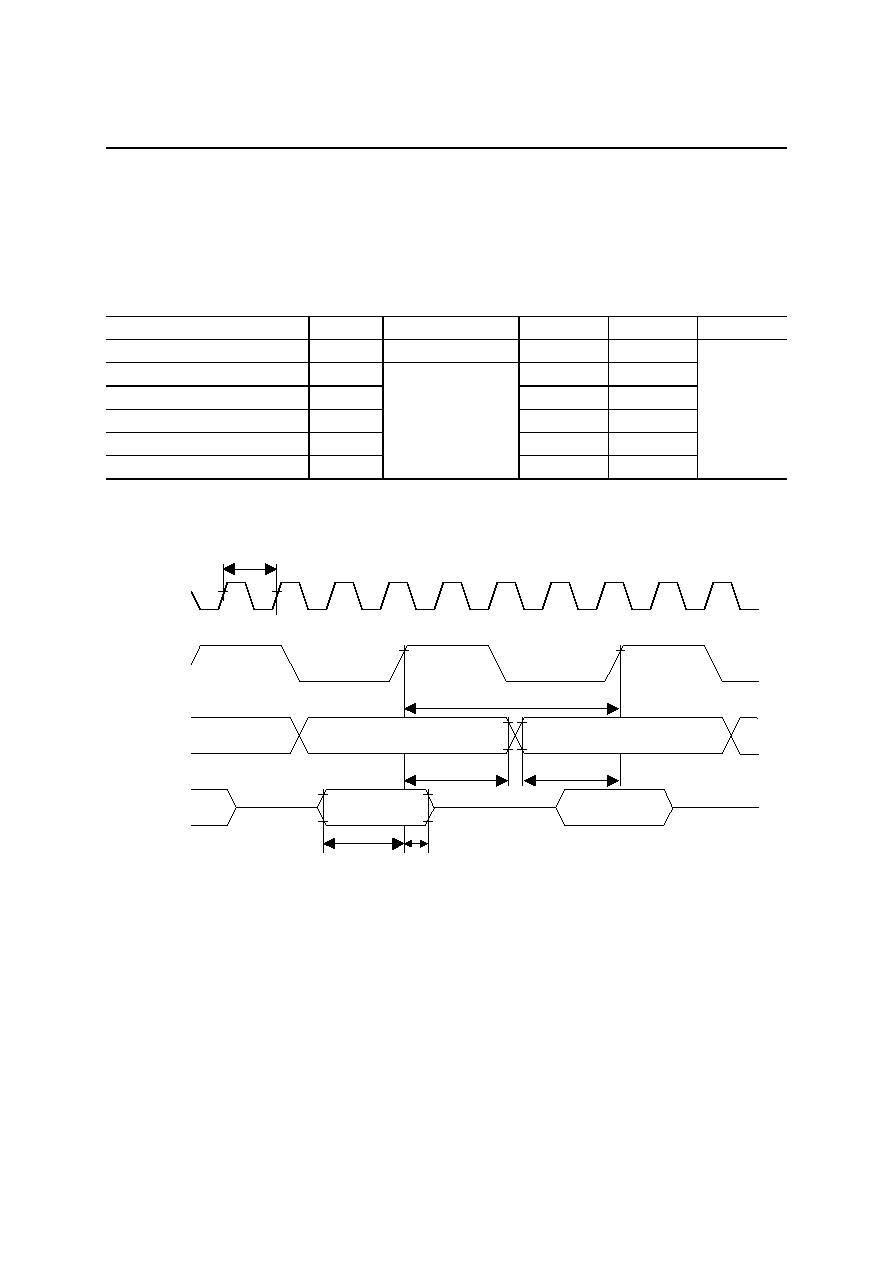
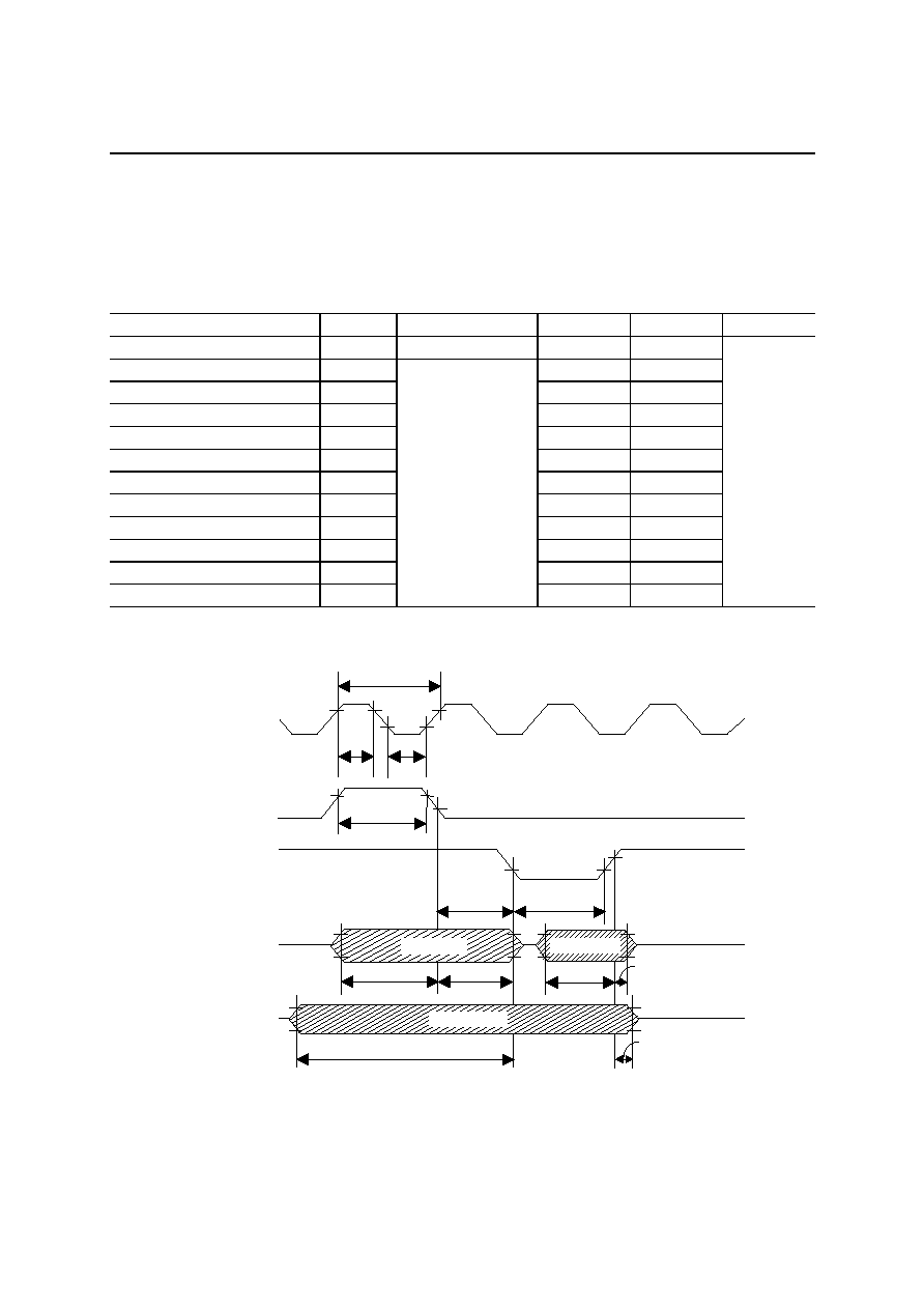
(3) Serial port control
Serial ports 1 and 6 (SIO1 and 6)
Master mode (Clock synchronous serial port)
(V
DD
= 4.5 to 5.5 V, Ta = �30 to +70�C)
Parameter
Symbol
Condition
Min.
Max.
Unit
Cycle time
t
cyc
f
OSC
= 30 MHz
33.3
--
Serial clock cycle time
t
SCKC
4 t
cyc
--
Output data setup time
t
STMXS
2 t
� 5
--
Output data hold time
t
STMXH
5 t
� 10
--
Input data setup time
t
SRMXS
13
--
Input data hold time
t
SRMXH
C
L
= 50 pF
0
--
ns
Note: t
= t
cyc
/2
t
cyc
CPUCLK
TXC/RXC
SDOUT
(TXD)
SDIN
(RXD)
t
STMXS
t
STMXH
t
SCKC
t
SRMXS
t
SRMXH
PEDL66579-03
1Semiconductor
MSM66579 Family
20/37
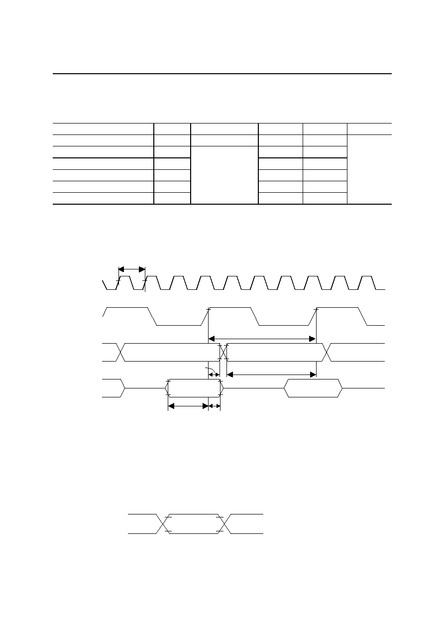
Slave mode (Clock synchronous serial port)
(V
DD
= 4.5 to 5.5 V, Ta = �30 to +70�C)
Parameter
Symbol
Condition
Min.
Max.
Unit
Cycle time
t
cyc
f
OSC
= 30 MHz
33.3
--
Serial clock cycle time
t
SCKC
4 t
cyc
--
Output data setup time
t
STMXS
2 t
� 15
--
Output data hold time
t
STMXH
4 t
� 10
--
Input data setup time
t
SRMXS
13
--
Input data hold time
t
SRMXH
C
L
= 50 pF
3
--
ns
Note: t
= t
cyc
/2
Measurement points for AC timing
0.8V
0.2V
0.8V
0.2V
V
DD
0 V
TXC/RXC
SDOUT
(TXD)
SDIN
(RXD)
t
STMXS
t
STMXH
t
SCKC
t
SRMXS
t
SRMXH
t
cyc
CPUCLK
PEDL66579-03
1Semiconductor
MSM66579 Family
21/37
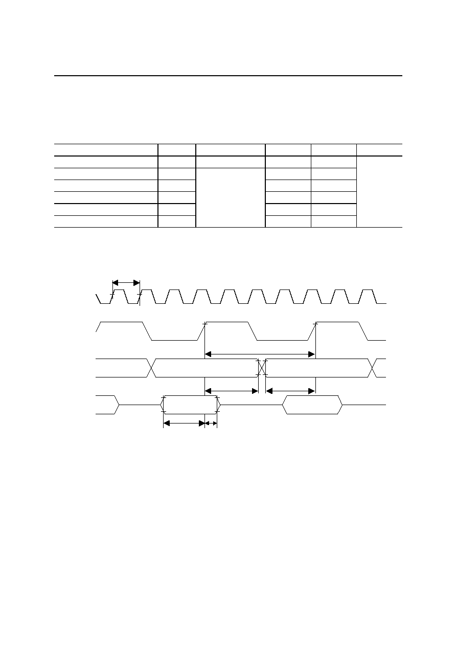
Serial ports 4 and 5 (SIO4 and 5)
Master mode (Clock synchronous serial port)
V
DD
= 4.5 to 5.5 V, Ta = �30 to +70�C)
Parameter
Symbol
Condition
Min.
Max.
Unit
Cycle time
t
cyc
f
OSC
= 30 MHz
33.3
--
Serial clock cycle time
t
SCKC
6 t
cyc
--
Output data setup time
t
STMXS
6 t
� 5
--
Output data hold time
t
STMXH
4.5 t
� 10
--
Input data setup time
t
SRMXS
13
--
Input data hold time
t
SRMXH
C
L
= 50 pF
0
--
ns
Note: t
= t
cyc
/2
SDIN
(SIOI)
SDOUT
(SIOO)
SIOCK
CPUCLK
t
cyc
t
STMXS
t
STMXH
t
SCKC
t
SRMXS
t
SRMXH
PEDL66579-03
1Semiconductor
MSM66579 Family
22/37
Slave mode (Clock synchronous serial port)
(V
DD
= 4.5 to 5.5 V, Ta = �30 to +70�C)
Parameter
Symbol
Condition
Min.
Max.
Unit
Cycle time
t
cyc
f
OSC
= 30 MHz
33.3
--
Serial clock cycle time
t
SCKC
6 t
cyc
--
Output data setup time
t
STMXS
3 t
� 15
--
Output data hold time
t
STMXH
6 t
� 10
--
Input data setup time
t
SRMXS
13
--
Input data hold time
t
SRMXH
C
L
= 50 pF
3
--
ns
Note: t
= t
cyc
/2
Measurement points for AC timing
0.8 V
0.2 V
0.8 V
0.2 V
V
DD
0 V
CPUCLK
(SIOI)
SDOUT
(SIOO)
SIOCK
SDIN
t
STMXS
t
STMXH
t
SCKC
t
SRMXS
t
SRMXH
t
cyc
PEDL66579-03
1Semiconductor
MSM66579 Family
23/37
AC Characteristics 2 (V
DD
= 2.4 to 3.6 V)
(1) Separate Bus Type
External program memory control
MSM66577L/579L (V
DD
= 2.4 to 3.6 V, Ta = �30 to +70�C)
MSM66Q577L/Q579L (V
DD
= 2.7 to 3.3 V, Ta = �30 to +70�C)
Parameter
Symbol
Condition
Min.
Max.
Unit
Cycle time
t
cyc
f
OSC
= 14 MHz
71.4
--
Clock pulse width (HIGH level)
t
WH
28
--
Clock pulse width (LOW level)
t
WL
28
--
PSEN pulse width
t
PW
2 t
� 20
--
PSEN pulse delay time
t
PD
--
75
Address setup time
t
AS
t
� 40
--
Address hold time
t
AH
0
18
Instruction setup time
t
IS
60
--
Instruction hold time
t
IH
0
--
Read data access time
t
ACC
C
L
= 50 pF
--
3 t
� 120
ns
Note: t
= t
cyc
/2
INST0 to 7
PC0 to 19
Bus timing during no wait cycle time
t
cyc
t
WH
CPUCLK
PSEN
A0 to A19
D0 to D7
t
WL
t
PD
t
PW
t
AS
t
ACC
t
IS
t
IH
t
AH
PEDL66579-03
1Semiconductor
MSM66579 Family
24/37
External data memory control
MSM66577L/579L (V
DD
= 2.4 to 3.6 V, Ta = �30 to +70�C)
MSM66Q577L/Q579L (V
DD
= 2.7 to 3.3 V, Ta = �30 to +70�C)
Parameter
Symbol
Condition
Min.
Max.
Unit
Cycle time
t
cyc
f
OSC
= 14 MHz
71.4
--
Clock pulse width (HIGH level)
t
WH
28
--
Clock pulse width (LOW level)
t
WL
28
--
RD pulse width
t
RW
2 t
� 20
--
WR pulse width
t
WW
2 t
� 20
--
RD pulse delay time
t
RD
--
75
WR pulse delay time
t
WD
--
75
Address setup time
t
AS
t
� 40
--
Address hold time
t
AH
t
� 6
t
+6
Read data setup time
t
RS
60
--
Read data hold time
t
RH
0
--
Read data access time
t
ACC
--
3t
�120
Write data setup time
t
WS
2t
� 40
--
Write data hold time
t
WH
C
L
= 50 pF
t
� 6
t
+ 6
ns
Note: t
= t
cyc
/2
DIN0 to 7
RAP0 to 19
t
RD
t
cyc
t
WH
CPUCLK
RD
A0 to A19
D0 to D7
DOUT0 to 7
RAP0 to 19
Bus timing during no wait cycle time
WR
A0 to A19
D0 to D7
t
WL
t
RW
t
AS
t
ACC
t
RS
t
WW
t
WD
t
AH
t
RH
t
AH
t
AS
t
WS
t
WH
PEDL66579-03
1Semiconductor
MSM66579 Family
25/37
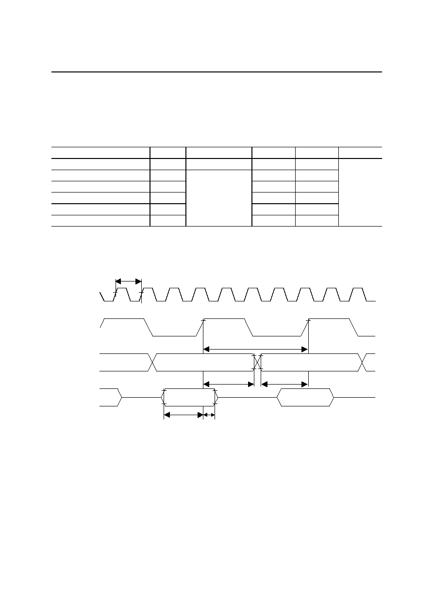
(2) Multiplexed bus type
External program memory control
MSM66577L/579L (V
DD
= 2.4 to 3.6 V, Ta = �30 to +70�C)
MSM66Q577L/Q579L (V
DD
= 2.7 to 3.3 V, Ta = �30 to +70�C)
Parameter
Symbol
Condition
Min.
Max.
Unit
Cycle time
t
cyc
f
OSC
= 14 MHz
71.4
--
Clock pulse width (HIGH level)
t
WH
28
--
Clock pulse width (LOW level)
t
WL
28
--
ALE pulse width
t
AW
2 t
� 15
--
PSEN pulse width
t
PW
2 t
� 18
--
PSEN pulse delay time
t
PAD
t
� 6
t
+ 6
Low address setup time
t
ALS
2t
� 40
2t
+ 6
Low address hold time
t
ALH
t
� 15
t
+ 15
High address setup time
t
AHS
3t
� 50
4t
+ 6
High address hold time
t
AHH
0
t
+ 15
Instruction setup time
t
IS
58
--
Instruction hold time
t
IH
C
L
= 50 pF
0
t
� 6
ns
Note: t
= t
cyc
/2
Bus timing during no wait cycle time
INST0 to 7
t
cyc
t
WH
CPUCLK
PSEN
A8 to A19
AD0 to AD7
ALE
PC0 to 7
PC8 to 19
t
WL
t
AW
t
PAD
t
PW
t
ALS
t
ALH
t
IS
t
IH
t
AHS
t
AHH
PEDL66579-03
1Semiconductor
MSM66579 Family
26/37
External data memory control
MSM66577L/579L (V
DD
= 2.4 to 3.6 V, Ta = �30 to +70�C)
MSM66Q577L/Q579L (V
DD
= 2.7 to 3.3 V, Ta = �30 to +70�C)
Parameter
Symbol
Condition
Min.
Max.
Unit
Cycle time
t
cyc
f
OSC
= 30 MHz
71.4
--
Clock pulse width (HIGH level)
t
WH
28
--
Clock pulse width (LOW level)
t
WL
28
--
ALE pulse width
t
AW
2 t
� 18
--
RD pulse width
t
RW
2 t
� 18
--
WR pulse width
t
WW
2 t
� 18
--
RD pulse delay time
t
RAD
t
� 6
t
+6
WR pulse delay time
t
WAD
t
� 6
t
+6
Low address setup time
t
ALS
2 t
� 12
2 t
Low address hold time
t
ALH
t
� 6
t
+6
High address setup time
t
AHS
3 t
� 12
3 t
+12
High address hold time
t
AHH
t
� 6
t
+6
Read data setup time
t
RS
48
--
Read data hold time
t
RH
0
t
� 6
Write data setup time
t
WS
2t
� 24
--
Write data hold time
t
WH
C
L
= 50 pF
t
� 6
t
+ 6
ns
Note: t
= t
cyc
/2
t
cyc
DIN0 to 7
RAP8 to 19
A
t
WH
CPUCLK
RD
A8 to A19
AD0 to AD7
ALE
RAP0 to 7
DOUT0 to 7
WR
A8 to A19
AD0 to AD7
RAP0 to 7
Bus timing during no wait cycle time
RAP8 to 19
t
WL
t
AW
t
RAD
t
RW
t
ALS
t
ALH
t
RS
t
RH
t
AHH
t
AHS
t
WAD
t
WW
t
WH
t
WS
t
ALS
t
ALH
t
AHH
t
AHS
PEDL66579-03
1Semiconductor
MSM66579 Family
27/37
(3) Serial port control
Serial ports 1 and 6 (SIO1 and 6)
Master mode (Clock synchronous serial port)
MSM66577L/579L (V
DD
= 2.4 to 3.6 V, Ta = �30 to +70�C)
MSM66Q577L/Q579L (V
DD
= 2.7 to 3.3 V, Ta = �30 to +70�C)
Parameter
Symbol
Condition
Min.
Max.
Unit
Cycle time
t
cyc
f
OSC
= 14 MHz
71.4
--
Serial clock cycle time
t
SCKC
4 t
cyc
--
Output data setup time
t
STMXS
2 t
� 10
--
Output data hold time
t
STMXH
5 t
� 20
--
Input data setup time
t
SRMXS
21
--
Input data hold time
t
SRMXH
C
L
= 50 pF
0
--
ns
Note: t
= t
cyc
/2
SDIN
(RXD)
SDOUT
(TXD)
TXC/RXC
CPUCLK
t
cyc
t
STMXS
t
STMXH
t
SCKC
t
SRMXS
t
SRMXH
PEDL66579-03
1Semiconductor
MSM66579 Family
28/37
Slave mode (Clock synchronous serial port)
MSM66577L/579L (V
DD
= 2.4 to 3.6 V, Ta = �30 to +70�C)
MSM66Q577L/Q579L (V
DD
= 2.7 to 3.3 V, Ta = �30 to +70�C)
Parameter
Symbol
Condition
Min.
Max.
Unit
Cycle time
t
cyc
f
OSC
= 14 MHz
71.4
--
Serial clock cycle time
t
SCKC
4 t
cyc
--
Output data setup time
t
STMXS
2 t
� 30
--
Output data hold time
t
STMXH
4 t
� 20
--
Input data setup time
t
SRMXS
21
--
Input data hold time
t
SRMXH
C
L
= 50 pF
7
--
ns
Note: t
= t
cyc
/2
Measurement points for AC timing
0.8 V
0.2 V
0.8 V
0.2 V
V
DD
0 V
t
cyc
TXC/RXC
SDOUT
(TXD)
SDIN
(RXD)
t
STMXS
t
STMXH
t
SCKC
t
SRMXS
t
SRMXH
CPUCLK
PEDL66579-03
1Semiconductor
MSM66579 Family
29/37
Serial ports 4 and 5 (SIO4 and 5)
Master mode (Clock synchronous serial port)
MSM66577L/ 579L (V
DD
= 2.4 to 3.6 V, Ta = �30 to +70�C)
MSM66Q577L/Q579L (V
DD
= 2.7 to 3.3 V, Ta = �30 to +70�C)
Parameter
Symbol
Condition
Min.
Max.
Unit
Cycle time
t
cyc
f
OSC
= 14 MHz
71.4
--
Serial clock cycle time
t
SCKC
5.6 t
cyc
--
Output data setup time
t
STMXS
5.6 t
� 10
--
Output data hold time
t
STMXH
4.2 t
� 20
--
Input data setup time
t
SRMXS
21
--
Input data hold time
t
SRMXH
C
L
= 50 pF
0
--
ns
Note: t
= t
cyc
/2
SDIN
(SIOI)
SDOUT
(SIOO)
SIOCK
CPUCLK
t
cyc
t
STMXS
t
STMXH
t
SCKC
t
SRMXS
t
SRMXH
PEDL66579-03
1Semiconductor
MSM66579 Family
30/37
Slave mode (Clock synchronous serial port)
MSM66577L/579L (V
DD
= 2.4 to 3.6 V, Ta = �30 to +70�C)
MSM66Q577L/Q579L (V
DD
= 2.7 to 3.3 V, Ta = �30 to +70�C)
Parameter
Symbol
Condition
Min.
Max.
Unit
Cycle time
t
cyc
f
OSC
= 14 MHz
71.4
--
Serial clock cycle time
t
SCKC
5.6 t
cyc
--
Output data setup time
t
STMXS
2.8 t
� 30
--
Output data hold time
t
STMXH
5.6 t
� 20
--
Input data setup time
t
SRMXS
21
--
Input data hold time
t
SRMXH
C
L
= 50 pF
7
--
ns
Note: t
= t
cyc
/2
Measurement points for AC timing
0.8 V
0.2 V
0.8 V
0.2 V
V
DD
0 V
CPUCLK
(SIOI)
SDOUT
(SIOO)
SIOCK
SDIN
t
STMXS
t
STMXH
t
SCKC
t
SRMXS
t
SRMXH
t
cyc
PEDL66579-03
1Semiconductor
MSM66579 Family
31/37
A/D Converter Characteristics 1 (V
DD
= 4.5 to 5.5 V)
(Ta = �30 to 70�C, V
DD
= V
REF
= 4.5 to 5.5 V, AGND = GND = 0 V)
Parameter
Symbol
Condition
Min.
Typ.
Max.
Unit
Resolution
n
--
10
--
Bit
Linearity error
E
L
--
--
�3
Differential linearity error
E
D
--
--
�2
Zero scale error
E
ZS
--
--
+3
Full-scale error
E
FS
Refer to measurement
circuit 1
Analog input source
impedance
R
I
5 k
t
conv
= 10.7 �s
--
--
�3
Cross talk
E
CT
Refer to measurement
circuit 2
--
--
�1
LSB
Conversion time
t
CONV
Set according to
ADTM set data
10.7
--
--
�s/ch
A/D Converter Characteristics 2 (V
DD
= 2.4 to 3.6 V)
(Ta = �30 to 70�C, V
DD
= V
REF
= 2.7 to 3.6 V, AGND = GND = 0 V)
Parameter
Symbol
Condition
Min.
Typ.
Max.
Unit
Resolution
n
--
10
--
Bit
Linearity error
E
L
--
--
�3
Differential linearity error
E
D
--
--
�2
Zero scale error
E
ZS
--
--
+3
Full-scale error
E
FS
Refer to measurement
circuit 1
Analog input source
impedance
R
I
5 k
t
conv
= 10.7 �s
--
--
�3
Cross talk
E
CT
Refer to measurement
circuit 2
--
--
�1
LSB
Conversion time
t
CONV
Set according to
ADTM set data
27.4
--
--
�s/ch
[Note] The A/D conversion time should be set according to ADTV set data. Set the number of
conversion clock cycles according to frequencies of operation so that the A/D conversion time is
32
�
s or more.
PEDL66579-03
1Semiconductor
MSM66579 Family
32/37
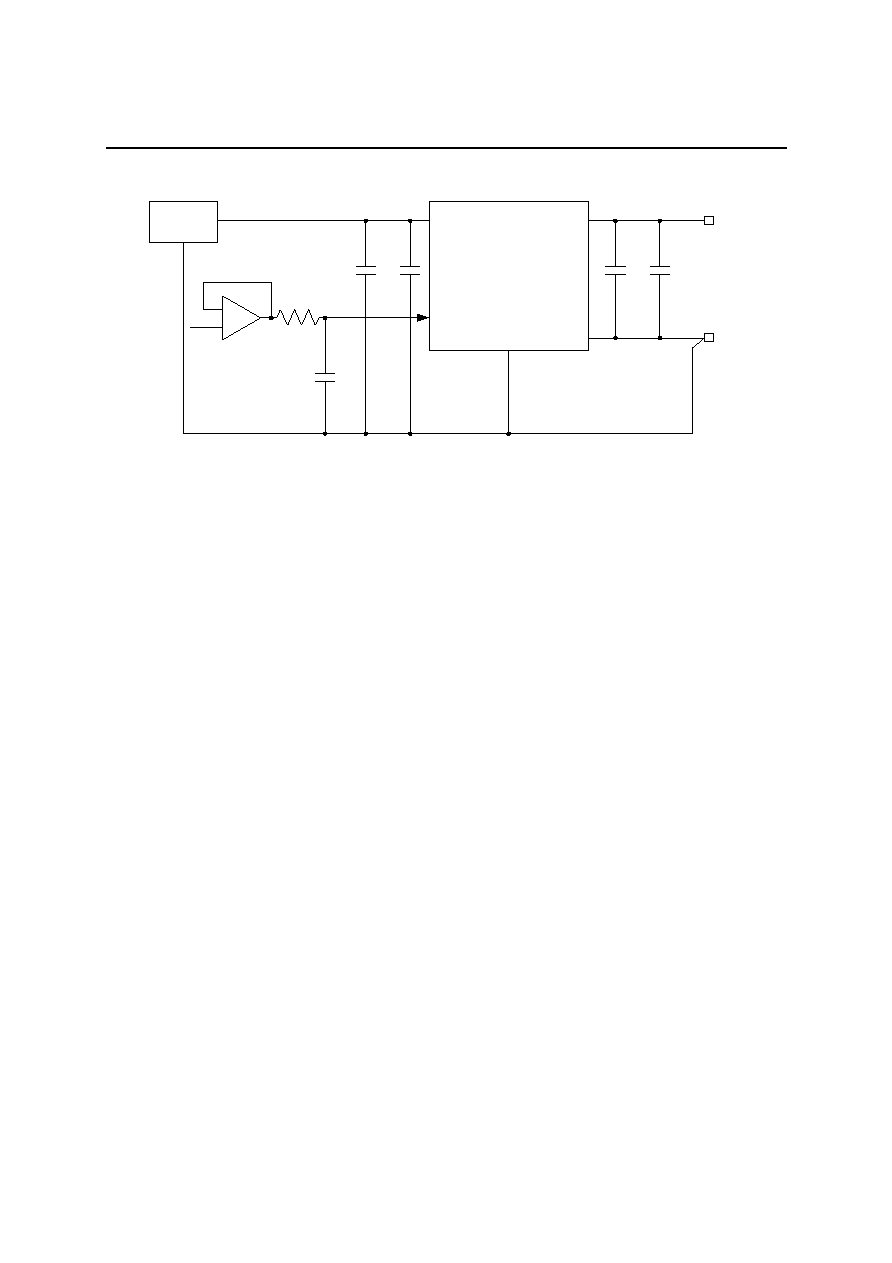
Measurement Circuit 1
V
REF
Reference
voltage
V
DD
GND
�
+
Analog input
R
I
AI0 to AI7
C
I
0.1
�
F
47
�
F
+
0.1
�
F
47
�
F
+
+5 V
0 V
AGND
R
I
(impedance of analog input source)
5 k
C
I
0.1
�
F
PEDL66579-03
1Semiconductor
MSM66579 Family
33/37
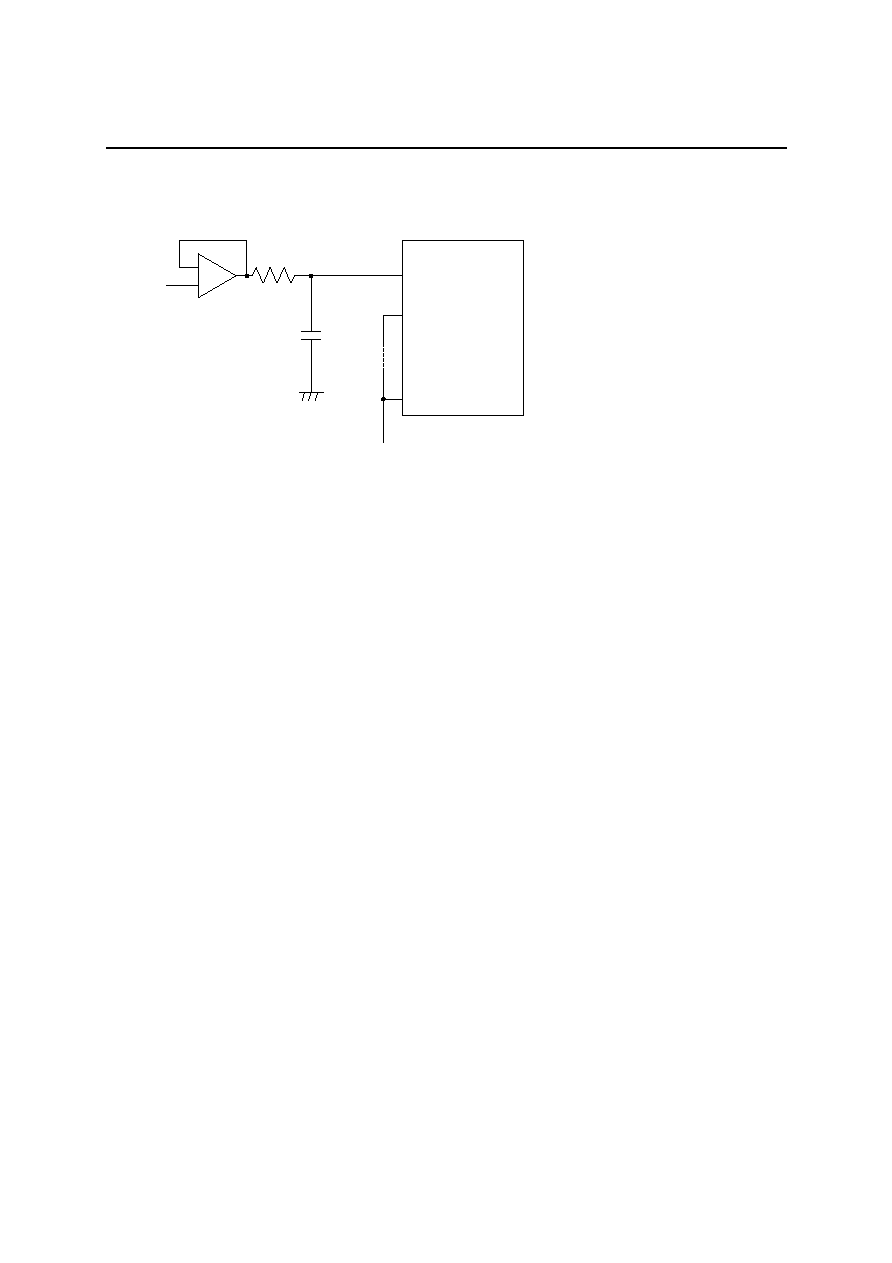
Measurement Circuit 2
Definition of Terminology
1. Resolution
Resolution is the value of minimum discernible analog input.
With 10 bits, since 2
10
= 1024, resolution of (V
REF
� AGND)
�
1024 is possible.
2. Linearity error
Linearity error is the difference between ideal conversion characteristics and actual conversion
characteristics of a 10-bit A/D converter (not including quantization error).
Ideal conversion characteristics can be obtained by dividing the voltage between V
REF
and AGND into 1024
equal steps.
3. Differential linearity error
Differential linearity error indicates the smoothness of conversion characteristics. Ideally, the range of analog
input voltage that corresponds to 1 converted bit of digital output is 1LSB = (V
REF
� AGND)
�
1024.
Differential error is the difference between this ideal bit size and bit size of an arbitrary point in the conversion
range.
4. Zero scale error
Zero scale error is the difference between ideal conversion characteristics and actual conversion characteristics
at the point where the digital output changes from 000H to 001H.
5. Full-scale error
Full-scale error is the difference between ideal conversion characteristics and actual conversion characteristics
at the point where the digital output changes from 3FEH to 3FFH.
�
+
Analog input
5 k
0.1
�
F
AI0
AI1
AI7
Cross talk is the difference
between the A/D conversion
results when the same
analog input is applied to AI0
through AI7 and the A/D
conversion results of the
circuit to the left.
to
V
REF
or AGND
PEDL66579-03
1Semiconductor
MSM66579 Family
34/37
D/A Converter Characteristics
(V
DD
= 2.4 to 3.6 V/4.5 to 5.5 V, Ta = �30 to +70�C)
Parameter
Symbol
Condition
Min.
Typ.
Max.
Unit
Resolution
n
--
--
8
Bit
Linearity error
E
L
--
--
1
Absolute precision
--
--
--
--
2
LSB
Conversion time
t
CONV
C
L
= 50 pF
--
20
50
�s
Analog output impedance
--
--
--
20
--
k
Definition of Terminology
1. Resolution
Resolution is the value of minimum discernible analog output.
With 8 bits, since 2
8
= 256, resolution of (V
DD
� GND)
�
256 is possible.
2. Linearity error
Linearity error is the difference between ideal conversion characteristics and actual conversion characteristics of
an 8-bit D/A converter.
Ideal conversion characteristics can be obtained by dividing the voltage between V
DD
and GND into 256 equal
steps.
3. Differential linearity error
Differential linearity error indicates the smoothness of conversion characteristics. Ideally, the range of analog
input voltage that corresponds to 1 converted bit of digital input is 1LSB = (V
DD
� GND)
�
256. Differential error
is the difference between this ideal bit size and bit size of an arbitrary point in the conversion range.
4. Absolute precision
Absolute precision is a gross error including a linearity error and the effect of noise.
PEDL66579-03
1Semiconductor
MSM66579 Family
35/37
PACKAGE DIMENSIONS
TQFP100-P-1414-0.50-K
Package material
Lead frame material
Pin treatment
Solder plate thickness
Package weight (g)
Epoxy resin
42 alloy
Solder plating
5 m or more
0.55 TYP.
Mirror finish
Notes for Mounting the Surface Mount Type Packages
The surface mount type packages are very susceptible to heat in reflow mounting and humidity
absorbed in storage. Therefore, before you perform reflow mounting, contact Oki's responsible sales
person on the product name, package name, pin number, package code and desired mounting
conditions (reflow method, temperature and times).
PEDL66579-03
1Semiconductor
MSM66579 Family
36/37
(Unit:mm)
QFP100-P-1420-0.65-BK
Package material
Lead frame material
Pin treatment
Solder plate thickness
Package weight (g)
Epoxy resin
42 alloy
Solder plating
5 m or more
1.29 TYP.
Mirror finish
Notes for Mounting the Surface Mount Type Packages
The surface mount type packages are very susceptible to heat in reflow mounting and humidity
absorbed in storage. Therefore, before you perform reflow mounting, contact Oki's responsible sales
person on the product name, package name, pin number, package code and desired mounting
conditions (reflow method, temperature and times).

PEDL66579-03
1Semiconductor
MSM66579 Family
37/37
NOTICE
1.
The information contained herein can change without notice owing to product and/or technical improvements.
Before using the product, please make sure that the information being referred to is up-to-date.
2.
The outline of action and examples for application circuits described herein have been chosen as an
explanation for the standard action and performance of the product. When planning to use the product, please
ensure that the external conditions are reflected in the actual circuit, assembly, and program designs.
3.
When designing your product, please use our product below the specified maximum ratings and within the
specified operating ranges including, but not limited to, operating voltage, power dissipation, and operating
temperature.
4.
Oki assumes no responsibility or liability whatsoever for any failure or unusual or unexpected operation
resulting from misuse, neglect, improper installation, repair, alteration or accident, improper handling, or
unusual physical or electrical stress including, but not limited to, exposure to parameters beyond the specified
maximum ratings or operation outside the specified operating range.
5.
Neither indemnity against nor license of a third party's industrial and intellectual property right, etc. is
granted by us in connection with the use of the product and/or the information and drawings contained herein.
No responsibility is assumed by us for any infringement of a third party's right which may result from the use
thereof.
6.
The products listed in this document are intended for use in general electronics equipment for commercial
applications (e.g., office automation, communication equipment, measurement equipment, consumer
electronics, etc.). These products are not authorized for use in any system or application that requires special
or enhanced quality and reliability characteristics nor in any system or application where the failure of such
system or application may result in the loss or damage of property, or death or injury to humans.
Such applications include, but are not limited to, traffic and automotive equipment, safety devices, aerospace
equipment, nuclear power control, medical equipment, and life-support systems.
7.
Certain products in this document may need government approval before they can be exported to particular
countries. The purchaser assumes the responsibility of determining the legality of export of these products
and will take appropriate and necessary steps at their own expense for these.
8.
No part of the contents contained herein may be reprinted or reproduced without our prior permission.
Copyright 1999 Oki Electric Industry Co., Ltd.