 | –≠–ª–µ–∫—Ç—Ä–æ–Ω–Ω—ã–π –∫–æ–º–ø–æ–Ω–µ–Ω—Ç: MSM66V84B | –°–∫–∞—á–∞—Ç—å:  PDF PDF  ZIP ZIP |

° Semiconductor
1/10
MSM66V84B
GENERAL DESCRIPTION
MSM66V84B is a serial register organized as 4,194,304 words x one bit, characterized by medium-
speed, low power consumption operation.
This device has a built-in internal address generation circuit allowing continuous serial read/write
operation by external clock input.
Read/write operation causes the internal address to be incremented automatically by +1.
External address input enables addressing in units of 1024 words. Furthermore, a refresh timer and
a refresh address counter are installed, which makes an external refresh circuit unnecessary. In
addition, this configuration allows lower power consumption.
The device is packaged in 26/20-pin SOJ or 26/20 TSOP having a width of 300 mil.
It is well adapted for storing much data by means of a battery backup. Its combination with our
recording and playback LSI enables the easy implementation of a solid recording and playback
system.
FEATURES
∑ Configuration
4,194,304 x 1 bit
∑ Serial access operation
Serial access time
: 1.5 ms
Serial read/write time : 2.5 ms
∑ Low current drain
100 mA max. (V
CC
= 3.6 V with data stored and under standard conditions)
∑ Refresh operation
A self-refresh function is supported.
∑ Wide operation voltage range
Single 2.7 to 3.6 V
∑ Addressing
Units of 1024 words
∑ Process
0.45 mm double well CMOS process
∑ Package options :
26/20-pin plastic SOJ (SOJ26/20-P-300-1.27) (Product name : MSM66V84BJS)
26/20-pin plastic TSOP (TSOPII26/20-P-300-1.27-K) (Product name : MSM66V84BTS-K)
° Semiconductor
MSM66V84B
4,194,304-word x 1-bit Serial Register
E2D0036-39-21
This version: Feb. 1999
Previous version: May. 1997
° Semiconductor
2/10
MSM66V84B
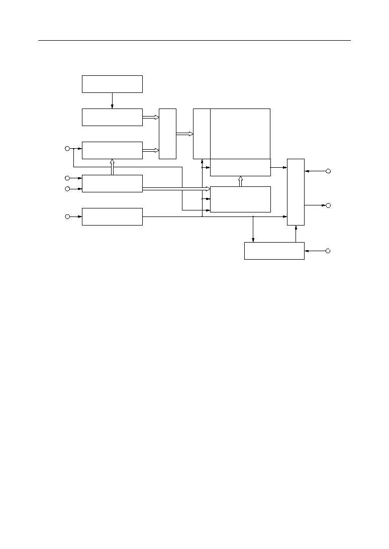
BLOCK DIAGRAM
Refresh Timer
Refresh Address
Counter
Row Address
Counter
Row Address
Register
Timing
Generator
TAS
SAD
SAS
RWCK
Address
Multiplexer
Row Decoder
4,194,304
Data Register
Column Decoder
Column Address
Counter
Write Clock
Generator
I/O Control
DIN
WE
DOUT
° Semiconductor
3/10
MSM66V84B
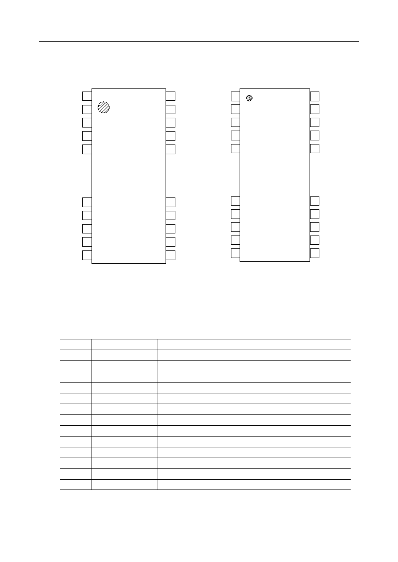
PIN CONFIGURATION (TOP VIEW)
Note : All TEST pins are to be connected to the power supply.
The TEST pin is to be referenced to the ground level.
Test input
Pin
Description
25
Test input
1, 4, 5
9, 10, 24
Read/write clock
2
Data input
11
Ground (0 V)
13
Data output
15
Write enable
16
Chip select
17
Transfer address strobe
18
Serial address strobe
22
Serial address data
23
Power supply (2.7 V to 3.6 V)
26
Symbol
TEST
TEST
RWCK
DIN
V
SS
DOUT
WE
CS
TAS
SAS
SAD
V
CC
3
NC
24 TEST
4
TEST
23 SAD
5
TEST
22 SAS
9
TEST
18 TAS
10
TEST
17 CS
11
DIN
16 WE
12
NC
15 DOUT
13
V
SS
14 NC
2
RWCK
25 TEST
1
TEST
26 V
CC
3
24 TEST
4
23 SAD
5
22 SAS
9
18 TAS
10
17 CS
11
16 WE
12
15 DOUT
13
14 NC
2
25 TEST
1
NC
TEST
TEST
TEST
TEST
DIN
NC
V
SS
RWCK
TEST
26 V
CC
PIN DESCRIPTION
NC : No connection
26/20-pin plastic SOJ
NC : No connection
26/20-pin plastic TSOP
(K type)
° Semiconductor
4/10
MSM66V84B
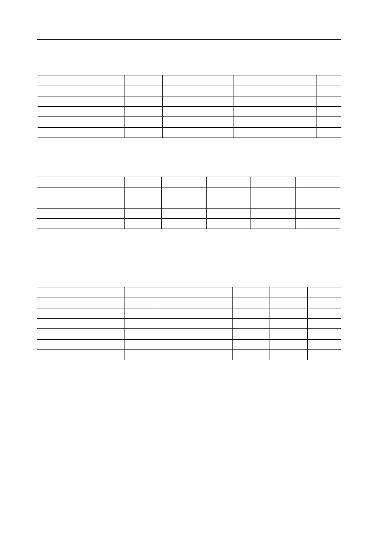
ABSOLUTE MAXIMUM RATINGS
Parameter
Symbol
Condition
Rating
Unit
Pin Voltage
V
T
Against V
SS
at Ta = 25 ∞C
≠0.5 to +4.6
V
Output Short-Circuit Current
Ta = 25 ∞C
50
mA
Power Dissipation
1
W
Operating Temperature
--
0 to 70
∞C
Storage Temperature
--
≠55 to +150
∞C
I
OS
P
D
T
op
T
STG
Ta = 25 ∞C
RECOMMENDED OPERATING CONDITIONS
Parameter
Symbol
Min.
Typ.
Max.
Unit
Supply Voltage
V
CC
2.7
3.0
3.6
Supply Voltage
0
0
0
"H" Input Voltage
V
CC
≠ 0.3
V
CC
V
CC
+ 0.2
"L" Input Voltage
≠0.2
0
+0.5
V
V
V
V
V
SS
V
IH
V
IL
(Ta = 0 to 70∞C)
ELECTRICAL CHARACTERISTICS
DC characteristics
Parameter
Symbol
Condition
Min.
Max.
Unit
"H" Output Voltage
V
OH
I
OH
= ≠0.1 mA
V
CC
≠ 0.5
--
V
"L" Output Voltage
I
OL
= 0.1 mA
--
0.4
V
Input Leakage Current
I
IL
V
I
= 0 V to V
CC
≠1
+1
mA
Output Leakage Current
V
O
= 0 V to V
CC
≠1
+1
mA
Supply Current (Operation)
V
CC
= 3.6 V, t
RWC
= 2.5 ms
--
10
mA
Supply Current (Standby)
V
CC
= 3.6 V
--
100
mA
V
OL
I
OL
I
CC1
I
CC2
(V
CC
= 2.7 V to 3.6 V, Ta = 0 to 70∞C)

° Semiconductor
5/10
MSM66V84B
AC Characteristics
Parameter
Symbol
Min.
Max.
Units
Read/Write Cycle Time
t
RWC
2,500
--
ns
Access Time
t
ACC
--
1,500
ns
Output Turn-off Delay Time
t
OFF
0
50
ns
I/O Signal Rise Time
t
T
3
50
ns
RWCK Pre-charge Time
t
RWP
1,000
--
ns
SAS Cycle Time
t
RW
1,500
10,000
ns
SAS Pre-charge Time
t
SSC
100
--
ns
SAS Pulse Width
t
SAP
50
--
ns
Address Setup Time
t
SAS
50
--
ns
Adress Hold Time
t
AS
0
--
ns
TAS Setup Time
t
AH
50
--
ns
TAS . RWCK Setup Time
t
ATS
50
--
ns
TAS Pulse Width
t
TRS
50
--
ns
Read Instruction Setup Time
t
TAS
50
--
ns
Read Instruction Hold Time
t
RRS
0
--
ns
Write Instruction Setup Time
t
RRH
250
--
ns
Write Instruction Hold Time
t
WRS
0
--
ns
Write Instruction Pulse Width
t
WRH
50
--
ns
WE. RWCK Read Time
t
WP
50
--
ns
Data Setup Time
t
RWL
50
--
ns
Data Hold Time
t
DS
0
--
ns
RWCK. WE Delay Time
t
DH
50
--
ns
t
RWD
50
--
ns
RWCK Pulse Time
(V
CC
= 2.7 V to 3.6 V, Ta = 0 to 70∞C)
° Semiconductor
6/10
MSM66V84B
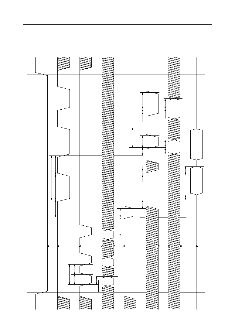
TIMING DIAGRAM
Read/write and read/modify/write cycles
CS
RWCK
SAS
SAD
TAS
WE
DIN
DOUT
t
TRS
t
RW
t
RWP
t
RWC
t
SSC
t
SAP
t
SAS
t
AH
t
AS
A0
A1
A12
n
n+1
n+1
n+2
t
ACC
t
OFF
t
DS
t
DH
t
DS
t
DH
t
WRH
t
WRS
t
WP
t
RWD
t
RRH
t
RRS
t
TAS
t
ATS
t
RWL

° Semiconductor
7/10
MSM66V84B
PIN FUNCTIONS AND OPERATING MODES
∑ Serial address input (SAD)
Pin used to enter start address for reading/writing. An address can be specified in units of 1024
words. 1024 words of address data can be entered through the pin as 13 bits (A0 to A12) of serial
data. The 13th bit must be A12 as a dummy address, however. The A12 input level must be either
"H" or "L".
∑ Serial address strobe (SAS)
This is a clock pin for latching serial address data into an internal register.
∑ Address transfer strobe (TAS)
This is an input pin for loading the internal address counter with serial address data latched in the
address register.
∑ Read/write clock (RWCK)
This is a clock input pin for reading and writing information in the data register. The trailing edge
of RWCK triggers off internal operation. In the reading mode, information in the data register is
output to the DOUT pin. In the writing mode, the data register is loaded with DIN information.
At the leading edge of RWCK, the internal address counter is incremented automatically by +1.
∑ Write enable (WE)
This is an input pin for selecting the read mode, the write mode, or the read-modify-write mode.
When WE is "H", the read mode is set up and, when WE is "L", the write mode is set up. When the
level is lowered from "H" to "L" with RWCK active, the read-modify-write mode is set up.
∑ Data input (DIN)
This is a pin for entering write data. Information on the data input pin is latched when the trailing
edge of RWCK is encountered in the write mode and that of WE is encountered in the read/modify
mode.
∑ Data output (DOUT)
The data output pin always provides high impedance as long as RWCK or CS is kept at "H". When
"H" or "L" information is read, the output pin set at "H" or "L", and information read until RWCK
returns to "H" is held. In the early write mode, the output pin is maintained at high impedance,
so that, connect of DIN and DOUT enables "I/O common operation".
∑ Chip selection (CS)
This is an input pin for disabling all input pins. This pin allows the use of two or more MSM66V84B
devices with data input and output pins connected in parallel.
∑ Test (TEST, TEST)
The TEST pin must always be fixed at "L" and the TEST pin at "H".

° Semiconductor
8/10
MSM66V84B
NOTES ON ENERGIZATION
MSM66V84B has built-in board bias generation and inner power supply circuits. Thus, energization
must be followed by a pause period of 1 ms or more for internal circuit stabilization. Furthermore,
the TEST pin must be brought "L" concurrently with or prior to V
CC
, and all clock input pins and TEST
pins must be brought "H" concurrently with or prior to V
CC
.
To achieve proper operation of internal circuits, the initial pause above must be followed by
minimum ten dummy read cycles with RWCK.
NOTES ON SUPPLY VOLTAGE VARIATION
When using MSM66V84B, take precautions so that the supply voltage does not vary over one volt
within a period of 1,000ms or less in the active state.
° Semiconductor
9/10
MSM66V84B
(Unit : mm)
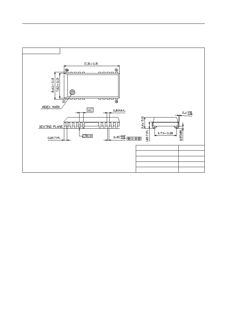
PACKAGE DIMENSIONS
Notes for Mounting the Surface Mount Type Package
The SOP, QFP, TSOP, TQFP, LQFP, SOJ, QFJ (PLCC), SHP, and BGA are surface mount type
packages, which are very susceptible to heat in reflow mounting and humidity absorbed in
storage. Therefore, before you perform reflow mounting, contact Oki's responsible sales person
on the product name, package name, pin number, package code and desired mounting conditions
(reflow method, temperature and times).
SOJ26/20-P-300-1.27
Package material
Lead frame material
Pin treatment
Solder plate thickness
Package weight (g)
Epoxy resin
42 alloy
Solder plating
5 mm or more
0.80 TYP.
Mirror finish
° Semiconductor
10/10
MSM66V84B
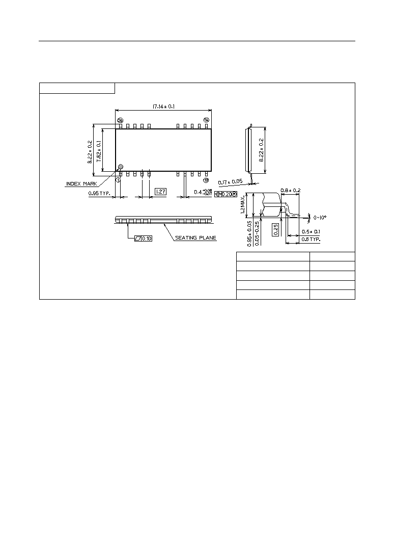
(Unit : mm)
Notes for Mounting the Surface Mount Type Package
The SOP, QFP, TSOP, TQFP, LQFP, SOJ, QFJ (PLCC), SHP, and BGA are surface mount type
packages, which are very susceptible to heat in reflow mounting and humidity absorbed in
storage. Therefore, before you perform reflow mounting, contact Oki's responsible sales person
on the product name, package name, pin number, package code and desired mounting conditions
(reflow method, temperature and times).
TSOP
II26/20-P-300-1.27-K
Package material
Lead frame material
Pin treatment
Solder plate thickness
Package weight (g)
Epoxy resin
42 alloy
Solder plating
5 mm or more
0.38 TYP.
Mirror finish

NOTICE
1.
The information contained herein can change without notice owing to product and/or
technical improvements. Before using the product, please make sure that the information
being referred to is up-to-date.
2.
The outline of action and examples for application circuits described herein have been
chosen as an explanation for the standard action and performance of the product. When
planning to use the product, please ensure that the external conditions are reflected in the
actual circuit, assembly, and program designs.
3.
When designing your product, please use our product below the specified maximum
ratings and within the specified operating ranges including, but not limited to, operating
voltage, power dissipation, and operating temperature.
4.
Oki assumes no responsibility or liability whatsoever for any failure or unusual or
unexpected operation resulting from misuse, neglect, improper installation, repair, alteration
or accident, improper handling, or unusual physical or electrical stress including, but not
limited to, exposure to parameters beyond the specified maximum ratings or operation
outside the specified operating range.
5.
Neither indemnity against nor license of a third party's industrial and intellectual property
right, etc. is granted by us in connection with the use of the product and/or the information
and drawings contained herein. No responsibility is assumed by us for any infringement
of a third party's right which may result from the use thereof.
6.
The products listed in this document are intended for use in general electronics equipment
for commercial applications (e.g., office automation, communication equipment,
measurement equipment, consumer electronics, etc.). These products are not authorized
for use in any system or application that requires special or enhanced quality and reliability
characteristics nor in any system or application where the failure of such system or
application may result in the loss or damage of property, or death or injury to humans.
Such applications include, but are not limited to, traffic and automotive equipment, safety
devices, aerospace equipment, nuclear power control, medical equipment, and life-support
systems.
7.
Certain products in this document may need government approval before they can be
exported to particular countries. The purchaser assumes the responsibility of determining
the legality of export of these products and will take appropriate and necessary steps at their
own expense for these.
8.
No part of the contents cotained herein may be reprinted or reproduced without our prior
permission.
9.
MS-DOS is a registered trademark of Microsoft Corporation.
Copyright 1999 Oki Electric Industry Co., Ltd.
Printed in Japan
E2Y0002-29-11