 | –≠–ª–µ–∫—Ç—Ä–æ–Ω–Ω—ã–π –∫–æ–º–ø–æ–Ω–µ–Ω—Ç: MSM6778 | –°–∫–∞—á–∞—Ç—å:  PDF PDF  ZIP ZIP |

1/7
° Semiconductor
MSM6778
GENERAL DESCRIPTION
The MSM6778 is a dot-matrix LCD common driver. Fabricated in CMOS technology, the device
contains two 60-bit bidirectional shift registers, two 60-bit level shifters, and two 60-bit 4-level
drivers.
The MSM6778 has 120 LCD outputs. The number of LCD outputs can be increased by cascading
MSM6778 devices, using cascade-connected I/O pins. The bias voltage which specifies a drive
level can optionally be supplied externally. The MSM6778 is suitable for various types of LCD
panel.
FEATURES
∑ Logic supply voltage
: 2.7 V to 5.5 V
∑ LCD drive voltage
: A wide range from 18 V to 28 V
∑ Applicable LCD duty
: 1/100 to 1/256
∑ The bias voltage can be externally supplied.
∑ Structure:
35mm-wide Tape Automated Bonding (TAB) film (Product name: MSM6778AV-Z-01)
Tin-plating
° Semiconductor
MSM6778
120-DOT COMMON DRIVER (TAB)
E2B0031-27-Y2
This version: Nov. 1997
Previous version: Mar. 1996
2/7
° Semiconductor
MSM6778
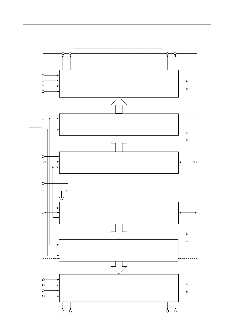
BLOCK DIAGRAM
60-BIT 4-LEVEL DRIVER
60-BIT LEVEL SHIFTER
60-BIT BI-DIRECTIONAL SHIFT REGISTER
60-BIT 4-LEVEL DRIVER
60-BIT BI-DIRECTIONAL SHIFT REGISTER
60-BIT LEVEL SHIFTER
O
1
O
2
O
59
O
60
V
DD
V
EE
V
DD
V
SS
V
DD
V
SS
V
DD
V
EE
IO
120
IO
60
O
120
O
119
O
62
O
61
V
EER
V
5R
V
2R
V
1R
V
EEL
V
5L
V
2L
V
1L
DF
DISPOFF
SHL
IO
1
CP
V
DDL,
V
DDR
V
SS
IO
61
3/7
° Semiconductor
MSM6778
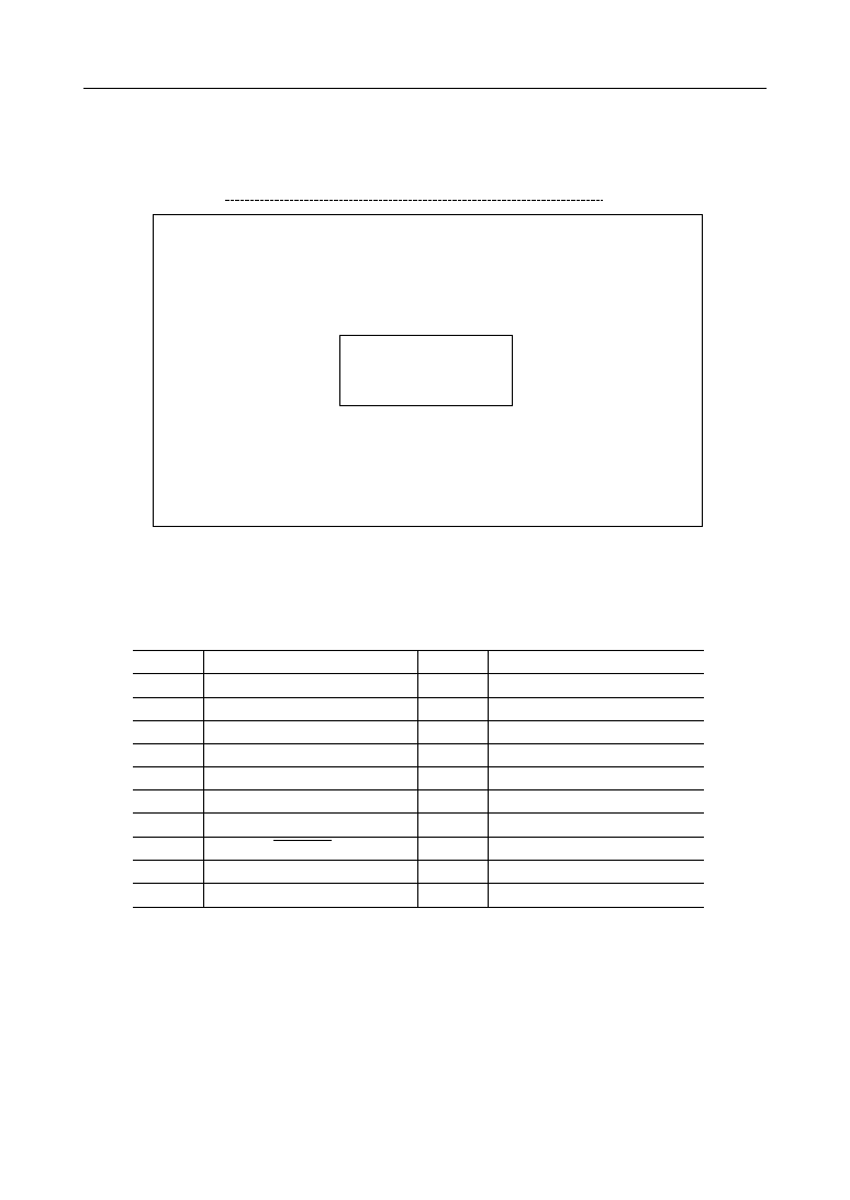
PIN CONFIGURATION (TOP VIEW)
Input Pin Name
Pin
Symbol
Pin
Symbol
1
2
3
4
5
6
7
8
9
10
19
18
17
16
15
14
13
12
11
V
1L
V
2L
V
5L
V
EEL
V
DDL
SHL
V
SS
DISPOFF
IO
1
IO
60
IO
61
IO
120
DF
CP
V
DDR
V
EER
V
5R
V
2R
V
1R
Chip surface
1 2 3 4 5 6 7 8 9 10 11 12 13 14 15 16 17 18 19
(Input pin side)
O
1
O
2
O
119
O
120
(LCD output side)
4/7
° Semiconductor
MSM6778
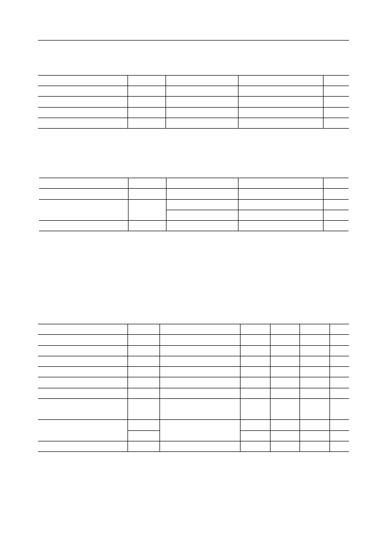
ABSOLUTE MAXIMUM RATINGS
RECOMMENDED OPERATING CONDITIONS
ELECTRICAL CHARACTERISTICS
DC Characteristics
Parameter
"H" Input Voltage
"L" Input Voltage
"H" Input Current
"L" Input Current
"H" Output Voltage
"L" Output Voltage
ON Resistance
Supply Current
Input Capacitance
Symbol
V
IH
*1
V
IL
*1
I
IH
*1
I
IL
*1
V
OH
*2
V
OL
*2
R
ON
*4
I
DD
*5
I
EE
*5
C
I
Condition
--
--
V
I
=V
DD
, V
DD
=5.5 V
V
I
=0 V, V
DD
=5.5 V
I
O
=≠0.2 mA, V
DD
=2.7 V
I
O
=0.2 mA, V
DD
=2.7 V
V
DD
≠V
EE
=25 V, *3
I V
N
≠V
O
I=0.25 V
f=1 MHz
Min.
0.8 V
DD
--
--
--
V
DD
≠0.4
--
--
--
--
--
Typ.
--
--
--
--
--
--
--
--
--
--
Max.
--
0.2 V
DD
1
≠1
0.4
2.0
60
400
--
Unit
V
V
mA
mA
V
V
kW
mA
mA
pF
CP=28 kHz, V
DD
=3.0 V
V
DD
≠V
EE
=25 V, No load
(V
DD
=2.7 to 5.5 V, Ta= ≠20 to +75∞C)
*1 Applicable to pins CP, IO
1
,IO
60
,IO
61
, IO
120
, SHL, DF, DISPOFF
*2 Applicable to pins IO
1
, IO
60
, IO
61
, IO
120
*3 V
N
=V
1
, V
2
, V
5
, V
EE
, V
2
=1/16 (V
DD
≠V
EE
), V
5
=15/16 (V
DD
≠V
EE
)
*4 Applicable to pins O
1
to O
120
*5 I
DD
shows the supply current between V
DD
and V
SS
. I
EE
shows the supply current between
V
DD
and V
EE
.
Note: The above values are guaranteed when TCP is protected from light.
Note:
Unlike mold packages, The Tape Carrier Package (TCP) cannot shield a light. Please
shield a light to secure the electrical characteristics.
* V
1
>V
2
>V
5
>V
EE
, V
DD
V
1
>V
2
V
DD
≠7V, V
EE
+7V V
5
>V
EE
V
DD
=V
DDL
=V
DDR
, V
1
=V
1L
=V
1R
, V
2
=V
2L
=V
2R
, V
5
=V
5L
=V
5R
, V
EE
=V
EEL
=V
EER
>
=
>
=
>
=
Parameter
Symbol
Condition
Range
Unit
Power Supply Voltage (1)
V
DD
--
2.7 to 5.5
V
Power Supply Voltage (2)
V
DD
≠V
EE
*
No load
14 to 28
V
During liquid crystal driving
18 to 28
V
Operating temperature
T
op
--
≠20 to +75
∞C
* V
1
>V
2
>V
5
>V
EE
, V
DD
V
1
>V
2
V
DD
≠10V, V
EE
+10V V
5
>V
EE
V
DD
=V
DDL
=V
DDR
, V
1
=V
1L
=V
1R
, V
2
=V
2L
=V
2R
, V
5
=V
5L
=V
5R
, V
EE
=V
EEL
=V
EER
>
=
>
=
>
=
Parameter
Symbol
Condition
Rating
Unit
Power Supply Voltage (1)
V
DD
Ta=25∞C
≠0.3 to +6.5
V
Power Supply Voltage (2)
V
DD
≠V
EE
*
Ta=25∞C
0 to 30
V
Input Voltage
V
I
Ta=25∞C
≠0.3 to V
DD
+0.3
V
Storage Temperature
T
STG
--
≠30 to +85
∞C
5/7
° Semiconductor
MSM6778
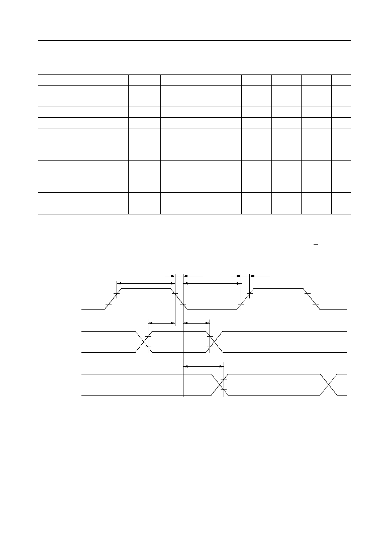
Switching Characteristics
Parameter
Symbol
Condition
Min.
Typ.
Max.
Unit
IO
1
, IO
61
(IO
60
, IO
120
)
"H", "L" Propagation Delay Time
Clock Frequency
CP Pulse Width
Data Setup Time
IO
1
, IO
61
∆ CP
(IO
60
, IO
120
∆ CP)
Data Hold Time
CP ∆ IO
1
, IO
61
(CP ∆ IO
60
, IO
120
)
CP Rise, Fall Time
t
PLH
t
PHL
f
CP
t
WCP
t
SETUP
t
HOLD
t
r (CP)
t
f (CP)
--
--
--
--
--
--
*1
--
63
100
100
--
--
--
--
--
--
--
3
1
--
--
--
20
ms
MHz
ns
ns
ns
ns
(V
DD
=2.7 to 5.5 V, Ta= ≠20 to +75∞C, C
L
=15 pF)
IO
1
(IO
60
)
IO
61
(IO
120
)
0.8V
DD
0.2V
DD
0.8V
DD
0.2V
DD
CP
t
WCP
t
f (CP)
t
r (CP)
0.8V
DD
0.8V
DD
0.2V
DD
0.2V
DD
IO
60
(IO
1
)
IO
120
(IO
61
)
t
SETUP
t
HOLD
t
PLH (
t
PHL)
t
WCP
*1 The relationship between t
PLH
(t
PLH
) Min. and t
HOLD
Min. satisfies the operation in a cascade
connection state.
Note 1: When display is controlled by DISPOFF pin, CP rise and fall time must be £ 1 ms.
Note 2: The above values are guaranteed when TCP is protected from light.
6/7
° Semiconductor
MSM6778
FUNCTIONAL DESCRIPTION
Pin Functional Description
∑ IO
1
, IO
60
, IO
61
, IO
120
These are I/O pins of the two 60-bit bidirectional shift registers.
∑ SHL
This pin selects the shift direction of the two 60-bit bidirectional shift registers.
Set this pin to "H" or "L" level during power-on.
SHL
Shift Direction
I/O pins
Function
L
H
O
1
∆ O
60
O
61
∆ O
120
O
60
∆ O
1
O
120
∆ O
61
IO
1
, IO
61
IO
60
, IO
120
IO
60
, IO
120
IO
1
, IO
61
Input
Output
Input
Output
IO
1
and IO
61
are data input pins for the shift
register. The entered data is read in at the falling
edge of a clock pulse. The data is output from
IO
60
and IO
120
behind the number of bits (60) of
the shift register.
IO
60
and IO
120
are data input pins for the shift
register. The entered data is read in at the falling
edge of a clock pulse. The data is output from IO
1
and IO
61
behind the number of bits (60) of the
shift register.
∑ CP
This is a clock pulse input for the two 60-bit bidirectional shift registers. Scan data is shifted at
the falling edge of a clock pulse.
∑ DF
This is a synchronous signal input for alternate signal for LCD driving.
∑ DISPOFF
This is an input used to control the output levels of O
1
to O
120
. During low level input, the V
1
level is output from the output pins O
1
to O
120
independently of the data of the shift register. See
the truth table.
∑ O
1
to O
120
These are outputs for the 4-level drivers, which correspond directly to each bit of the shift
register. One of the four levels V
1
, V
2
, V
5
, and V
EE
is selected and output depending on the
combination of the shift register data and a DF signal. See the Truth Table.
∑ V
1L
, V
2L
, V
5L
, V
EEL
, V
1R
, V
2R
, V
5R
, V
EER
These are LCD drive bias voltage inputs.
∑ V
DDL
, V
DDR
, V
SS
These are power supply pins for the device. V
DD
is usually from 2.7 V to 5.5 V and V
SS
is 0 V.

7/7
° Semiconductor
MSM6778
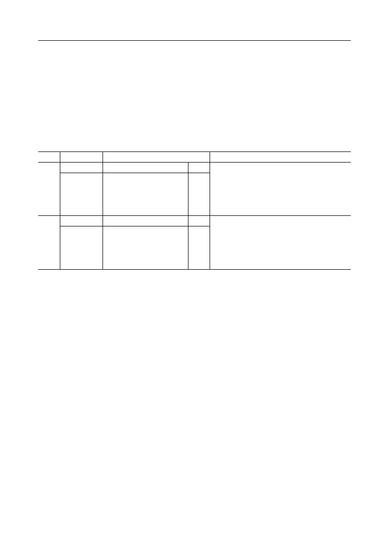
Truth Table
DF
L
L
H
H
X
SHIFT REGISTER DATA
L
H
L
H
X
DISPOFF
H
H
H
H
L
DRIVER OUTPUT (O
1
to O
120
)
V
2
V
EE
V
5
V
1
V
1
X : Don't care
NOTES ON USE (when turning the power ON or OFF)
The LCD drivers of this IC require a high voltage. For this reason, if a high voltage is applied to
the LCD drivers with the logic power supply floating, excess current flows. This may damage
the IC.
Be sure to follow the sequence below when turning the power ON or OFF.
Power ON : Logic circuits ON ∆ LCD drivers ON, or both ON at a time
Power OFF : LCD drivers OFF ∆ logic circuits OFF, or both OFF at a time