
120
° Semiconductor
MSM6782-01
° Semiconductor
MSM6782-01
REAL TIME CLOCK
GENERAL DESCRIPTION
The MSM6782 - 01 is a CMOS Serial Interface Real Time Clock/Calendar.
The serial interface that can be controlled by mere 3 signal lines has minimized the number of
CPU terminals required .
The MSM6782 - 01 provides 30-second adjustment, oscillation stop detection, and periodic flag
setting and signal output in 4 diferent cycle periods.
The clock ranges are seconds, minutes, hours, days, months, years, and days of the week.
The interface supply voltage is 2.7V to 5.5V and the clock supply voltage is 2.0V to 5.5V.
The MSM6782 - 01 comes in an 8-pin DIP package or an 8-pin SOP package.
The MSM6782 - 01 is highly integrated and is suitable for use in a variety of portable applications.
FEATURES
∑ Real time clock providing seconds, minutes, hours, days, months, and days of the week.
∑ Serial interface controlled by 3 signal lines
∑ A periodic interrupt output in 4 different cycle periods (or periodic waveform output)
∑ Automatic leap year calendar
∑ 30-second adjustment controlled by software
∑ Stop and restart of clock
∑ Wide range of interface power supply: 2.7V to 5.5V
∑ Wide range of clock power supply: 2.0V to 5.5V
∑ 32.768kHz external quart crystal
∑ Low current consumption
∑ 8-pin plastic DIP (DIP8-P-300) (MSM6782-01RS)
∑ 8-pin plastic SOP (SOP8-P-250-K) (MSM6782-01MS-K)
121
MSM6782-01
° Semiconductor
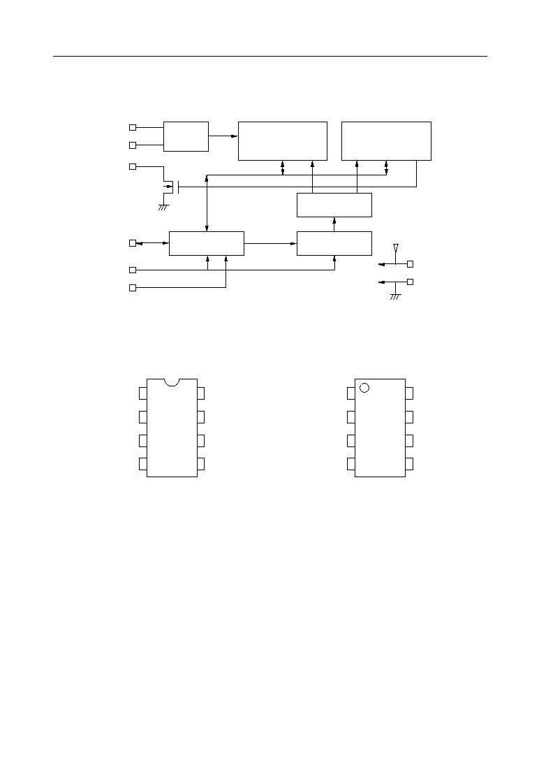
BLOCK DIAGRAM
XT
OSC
XT
Clock/calendar
registers
Control registers
(C
D
, C
E
, C
F
)
Decoder
Data buffer
Address counter
STD.P
CLK
DATA I/O
CE
V
DD
V
SS
PIN CONFIGURATION
The actual type name is displayed
as 6782-01.
The actual type name is displayed
as 82-01.
1
2
3
4
8
7
6
5
V
DD
XT
XT
V
SS
STD.P
DATA I/O
CLK
CE
1
2
3
4
8
7
6
5
V
DD
XT
XT
V
SS
STD.P
DATA I/O
CLK
CE
8-Pin Plastic SOP
8-Pin Plastic DIP
Note :
Note :
122
° Semiconductor
MSM6782-01
PIN DESCRIPTION
∑ STD.P (Pin No. 1)
Periodic output of N-CH OPEN DRAIN type or interrupt signal output of N-CH OPEN
DRAIN type for the CPU. The periodic output is used to check the reference signal and
oscillation frequency.
This pin is set as periodic output or interrupt signal output by writing "1" or "0" to the INT/
STND bit.
This output is not inhibited by CE. For more information, see "FUNCTIONAL DESCRIP-
TION OF REGISTERS".
∑ DATA I/O (Pin No.2)
Input/output pin for setting of WRITE mode or READ mode, writing of addresses, or
writing/reading of data.
This pin is used as an input or output pin in high impedance state depending on whether
WRITE mode or READ mode is selected in the first 8-bit data cycle after the rising of the CE
input pulse.
∑ CLK (Pin No. 3)
Shift clock input pin. Data is taken in on the rising edge of a shift clock pulse when in WRITE
mode and data is output when in READ mode.
∑ CE (Pin No. 4)
Chip enable input pin. "H" level on this pin means "enable".
When this pin is low, the DATA I/O pin goes into high impedance state, and DATA I/O and
CLK are disabled inside the LSI and current stops flowing through those pins.
"L" level on this pin forces the TEST and REST bits of the C
F
registers and the fr flag to be set
to "0".
When turning the power ON, set this pin to "L" level.
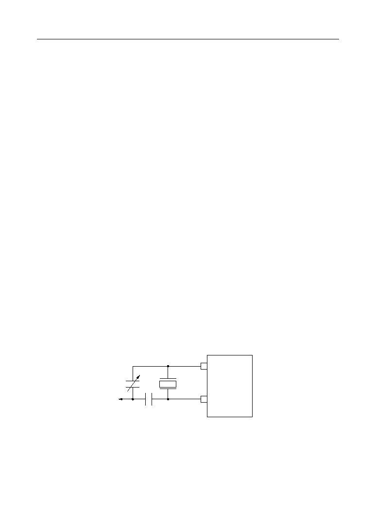
∑ XT, XT (Pin Nos. 7 and 6)
32.768kHz crystal is to be connected to these pins.
XT
XT
MSM6782-01
XT
V
DD
C
1
C
2
When an external clock is used, it is to be input from XT, while XT should be left open.
The oscillation crystal and capacitors should be placed as close to the IC as possible.
The oscillation circuit and other signal lines on any side of the LSI should be distant from each
other.
∑ V
DD
, V
SS
(Pin No.5)
Power supply pins. V
DD
is used for positive supply and V
SS
is for negative supply.
123
MSM6782-01
° Semiconductor
ABSOLUTE MAXIMUM RATINGS
RECOMMENDED OPERATING CONDITIONS
(Note) Clock power supply : Crystal oscillation and clock must be assured
ELECTRICAL CHARACTERISTICS
DC Characteristics
Parameter
Symbol
Unit
Rating
Condition
Power supply voltage
V
DD
--
Input voltage
Output voltage
Storage temperature
V
I
V
O
T
STG
Ta = 25∞C
≠0.3 to 7.0
V
ss
≠0.3 to V
DD
+0.3
V
ss
≠0.3 to V
DD
+0.3
≠55 to +150
∞C
V
Parameter
Symbol
Unit
Rating
Condition
Power supply voltage
V
DD
--
Clock power supply
Crystal frequency
Operating temperature
V
CLK
f
X
T
OP
2.7 to 5.5
2.0 to 5.5
32.768
≠40 to +85
∞C
V
--
--
--
V
kHz
Parameter
Symbol
Applicable
terminal
MIN
Condition
"H" Input Voltage
V
IH
--
TYP
MAX Unit
(V
DD
= 2.7 to 5.5.V, Ta = ≠40 to +85∞C)
"L" Input Voltage
"H" Input Current (1)
"L" Input Current (1)
"H" Input Current (2)
"L" Input Current (2)
"L" Output Current (1)
"H" Output Current
"L" Output Current (2)
OFF Leak Current
Current Consumption(2)
V
IL
I
IH1
I
IL1
I
IH2
I
IL2
V
OL1
V
OH
V
OL2
V
OFLK
V
DD2
V
I
=V
DD
V
I
=V
SS
V
I
=V
DD
V
I
=V
SS
I
O
=1.0mA
I
O
=≠400mA
I
O
=1.0mA
V
O
=V
DD
V
DD
=2V
--
0.8V
DD
--
--
--
--
--
--
0.8V
DD
--
--
--
--
--
--
--
--
--
--
--
--
--
--
--
0.2V
DD
1
≠1
10
≠10
0.2V
DD
--
0.2V
DD
10.0
2.5
V
V
mA
mA
mA
mA
V
V
V
mA
mA
All input pins
except XT
CE, CLK
CE, CLK
DATA I/O
DATA I/O
DATA I/O
DATA I/O
STD.P
STD.P
V
DD
Current Consumption(1)
V
DD1
V
DD
=5V
--
--
20.0
mA
V
DD
f
X
=32.768kHz
V
I
(CE)=0V
124
° Semiconductor
MSM6782-01
∑
AC Characteristics
(Note) See Timing Chart.
Parameter
Symbol
MIN
Condition
CLK "H" Pulse Width
t
WH
--
TYP
MAX
Unit
(V
DD
= 2.7 to 5.5V, Ta = ≠40 to +85∞C)
CLK "L" Pulse Width
CE Setup Time
CE Hold Time
CE Recovery Time
CLK Setup Time
CLK Hold Time
WRITE Data Setup Time
WRITE Data Hold Time
READ Data Delay Time
Input Rise, Fall Time
C
L
= 50pF
--
300
300
150
200
300
20
20
50
50
--
--
--
--
--
--
--
--
--
--
--
--
--
--
250
20
ns
Output Disable Delay Time
--
--
100
--
--
--
--
--
--
--
--
--
ns
ns
ns
ns
ns
ns
ns
ns
ns
ns
ns
--
--
--
--
--
--
--
--
t
WL
t
CS
t
CH
t
CR
t
CKS
t
CKH
t
DS
t
DH
t
RD
t
RZ
t
RF
125
MSM6782-01
° Semiconductor
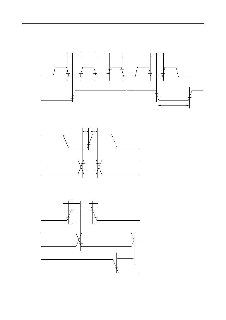
TIMING CHART
CLK
t
CR
V
IL
CE
V
IL
V
IL
V
IL
V
IL
V
IL
V
IH
V
IH
V
IL
V
IL
t
CKS
t
CS
t
WL
t
WH
V
IH
V
IH
t
CH
t
CKH
WRITE mode
CLK
V
IL
V
IH
V
IL
t
DS
V
IH
V
IL
DATA I/O
V
IH
t
DH
READ mode
CLK
V
OH
HiZ
V
IL
DATA I/O
V
IH
t
RZ
V
OL1
CE
V
IL
V
IH
V
IL
t
RF
t
RD
t
RF
126
° Semiconductor
MSM6782-01
FUNCTIONAL DESCRIPTION
REGISTER TABLE
∑ The relation between the register's bit 0 and bit 1 is logically positive as 0="L" and 1="H".
∑ The counted values are in BCD notation.
For example, with 1-year register (Y
1
), (y
8
, y
4
, y
2
, y
1
) = (0, 0, 1, 0) means the last digit ("2") of
"1992".
∑ Bit * also can be used as RAM.
∑ It is unexecutable to write data into the IRQ-F bit.
The IRQ-F bit is set to "1" when a specified carry determined by the combination of t
1
and t
0
is executed.
The IRQ-F bit holds "1" until the reading of C
D
is complete and is reset to "0" automatically
after the reading of C
D
is complete .
∑ The bit fo (OSC FLAG) memorizes that oscillation stops.
This bit is used to monitor the battery.
This bit is cleared by writing a "0". (A "1" also can be written into this bit.)
∑ The bit f
r
(READ FLAG) goes "0" when the CE pin is set at "L" level and goes "1" when a carry
occurs for 1-second digit while the CE input is at "H" level.
Thus, it is possible to judge whether a carry occurs for 1-second digit during the reading of
the clock register (CE input = "H").
If the bit f
r
is set at "1", it is required to read the clock register once more.
∑ The "1" of the PM/AM bit indicates PM and its "0" indicates AM.
Register
name
1-second digit register
S
1
0
Note
A3A2A1A0
D3
(MSB)
D2
D1
D0
(LSB)
Count
range
1
2
3
4
5
6
7
8
9
A
B
C
D
E
F
HEX
0 0 0 0
0 0 0 1
0 0 1 0
0 0 1 1
0 1 0 0
0 1 0 1
0 1 1 0
0 1 1 1
1 0 0 0
1 0 0 1
1 0 1 0
1 0 1 1
1 1 0 0
1 1 0 1
1 1 1 0
1 1 1 1
S
10
MI
1
MI
10
H
1
H
10
D
1
D
10
MO
1
MO
10
Y
1
Y
10
W
C
D
C
E
C
F
s
8
f
O
mi
8
f
r
h
8
f
r
d
8
f
r
mo
8
f
r
y
8
y
80
f
r
30-secADJ
t
1
TEST
s
4
s
40
mi
4
mi
40
h
4
PM/AM
d
4
*
mo
4
*
y
4
y
40
w
4
IRQ-F
t
0
24/12
s
2
s
20
mi
2
mi
20
h
2
h
20
d
2
d
20
mo
2
*
y
2
y
20
w
2
CAL/HW
INT/STND
STOP
s
1
s
10
mi
1
mi
10
h
1
h
10
d
1
d
10
mo
1
mo
10
y
1
y
10
w
1
HOLD
MASK
REST
0 to 9
0 to 5
0 to 9
0 to 5
0 to 9
0 to 1, 2
0 to 9
0 to 3
0 to 9
0 to 1
0 to 9
0 to 9
0 to 6
--
--
--
10-second digit register
1-minute digit register
10-minute digit register
1-hour digit register
10-hour digit register
1-day digit register
10-day digit register
1-month digit register
10-month digit register
1-year digit register
10-year digit register
Week digit register
Control register D
Control register E
Control register F
127
MSM6782-01
° Semiconductor
FUNCTIONAL DESCRIPTION OF REGISTERS
Registers S
1
, S
10
, MI
1
, MI
10
, H
1
, H
10
, D
1
, D
10
, MO
1
, MO
10
, Y
1
, Y
10
, W
∑ These are abbreviations for Second
1
, Second
10
, MInute
1
, MInute
10
, Hour
1
, Hour
10
, Day
1
,
Day
10
, MOnth
1
, MOnth
10
, Year
1
, Year
10
, Week.
These values are in BCD notation.
∑ Refer to the REGISTER TABLE for more detalied information.
All registers are logically positive.
For example, (S
8
, S
4
, S
2
, S
1
) = 1001 means 9 seconds.
The * bit in the register table is writable/readable and can be used as RAM.
∑ Writing non-existant data may cause a clocking error.
∑ PM/AM, h
20
, h
10
a) In 12-hour mode
The existant time is AM 12:00 through AM 11:00 and PM 12:00 through PM 11:00.
It is impossble to write data into the h
20
bit which is fixed to "0" unconditionally. The h
20
bit is not set by clocking.
b) In 24-hour mode
The existant time is 0:00 clock through 23:00 clock.
The PM/AM bit written is ignored and read out as "0" unconditionally.
∑ Registers Y
1
, Y
10
, and Leap Year
When using the Christian Era calendar, Y
1
and Y
10
are assigned to the last 2 digits of the year
of Christian Era.
The MSM6782 - 01 is capable of automatically identifying a leap year when the last 2-digit
number of the year can be divided by four. The last 2-digit number 99 changes to 00 next year.
∑ Register W
The count range of the register W is 0 ~ 6. The following table shows a possible bit data
definition.
0
W
4
W
2
W
1
Day of Week
0
0
0
1
1
1
0
0
1
1
0
0
1
0
1
0
1
0
1
0
Sunday
Monday
Tuesday
Wednesday
Thursday
Friday
Saturday
∑ f
o
Flag
The f
o
flag bit memorizes that oscillation stops and is used to monitor the output of the battery.
The "1" of this bit indicates stop of oscillation. This bit is cleared by writing "0". It is not
permitted to write "1" into this bit.

128
° Semiconductor
MSM6782-01
∑ f
r
Flag
The f
r
flag bit indicates a carry when the CE input is at "H" level.
This bit is checked when the clock/calendar registers are read out. If this bit is set to "1", it
is possible to read out these registers without using the HOLD bit.
This bit is cleared by setting the CE input to "L" level.
C
D
REGISTER (Control D Register)
∑ 30-sec ADJ (30-second adjustment bit)
When writing to this bit, if the second digits are smaller than 30, the second digits are reset
to 00, and if it is larger than 30, the second digits are reset to 00 and a carry into the minute
digit is executed. Data can not be written into the S
1
~ W registers and a "1" can not be written
into the REST bit of the C
F
register 125ms after writing into this bit because internal processing
is being executed. This bit holds "1" 125ms after writing, and returns to "0" automatically.
Therefore, data should be written into the S
1
~ W registers after checking that this bit has
returned to "0".
∑ IRQ - F
This bit is set to "1" and the STD.P output goes low in the cycle period specified by the
combination of bit t
1
and bit t
0
of the C
E
register. If INT/STND = "1", the bit status "1" and
output level "L" are kept until reading of the C
D
register is complete.
After the C
D
register is read out, the IRQ - F bit returns to "0" and the STD.P output goes into
high impedance automatically.
If INT/STD = "0", the IRQ -F bit returns to "0" about 7.8 ms later or immediately after the C
D
register is read out, and the STD.P returns to "high impedance" about 7.8 ms later.
∑ CAL/HW (Clock range switching bit)
CAL/HW = "1" : Seconds, minutes, hours, days, month, year, day of week
CAL/HW = "0" : Seconds, minutes, hours, day of week
If this bit is "0", the D
1
, D
10
, MO
1
, MO
10
, Y
1
, Y
10
registers can be used as 4-bit data RAM and
the * bits and f
r
bits of the D
10
and MO
10
registers also can be used as independent RAM,
because these registers stop clock operation.
∑ HOLD
"1" of this bit inhibits a carry into 1-second digit.
Clock operation continues before reaching a second.
During Hold = "1", if a carry occurs, the S1 counter is incremented by 1 second after Hold =
"0".
This bit is cleared to zero by writing "0".
129
MSM6782-01
° Semiconductor
C
E
REGISTER (Control E Register)
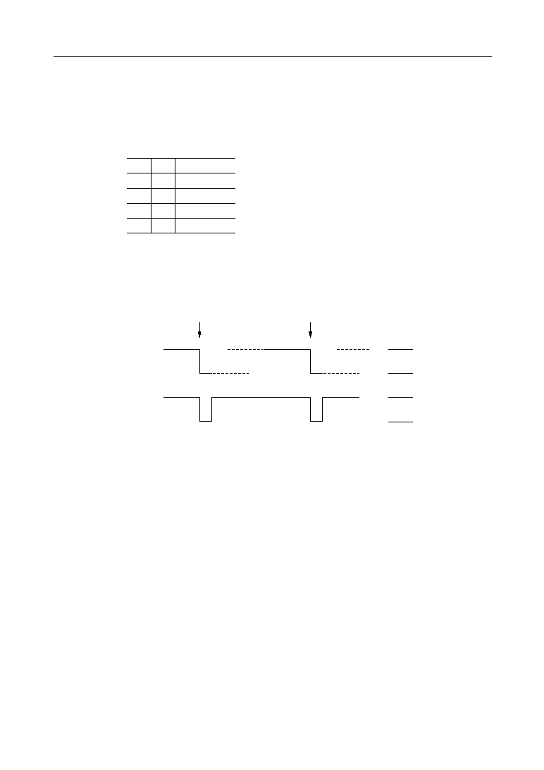
∑ t
1
, t
0
INT/STND bit = "1" : Setting of interrupt period
INT/STND bit = "0" : Setting of periodic waveform
t
1
0
0
1
1
1/64 second
1 second
1 minute
1 hour
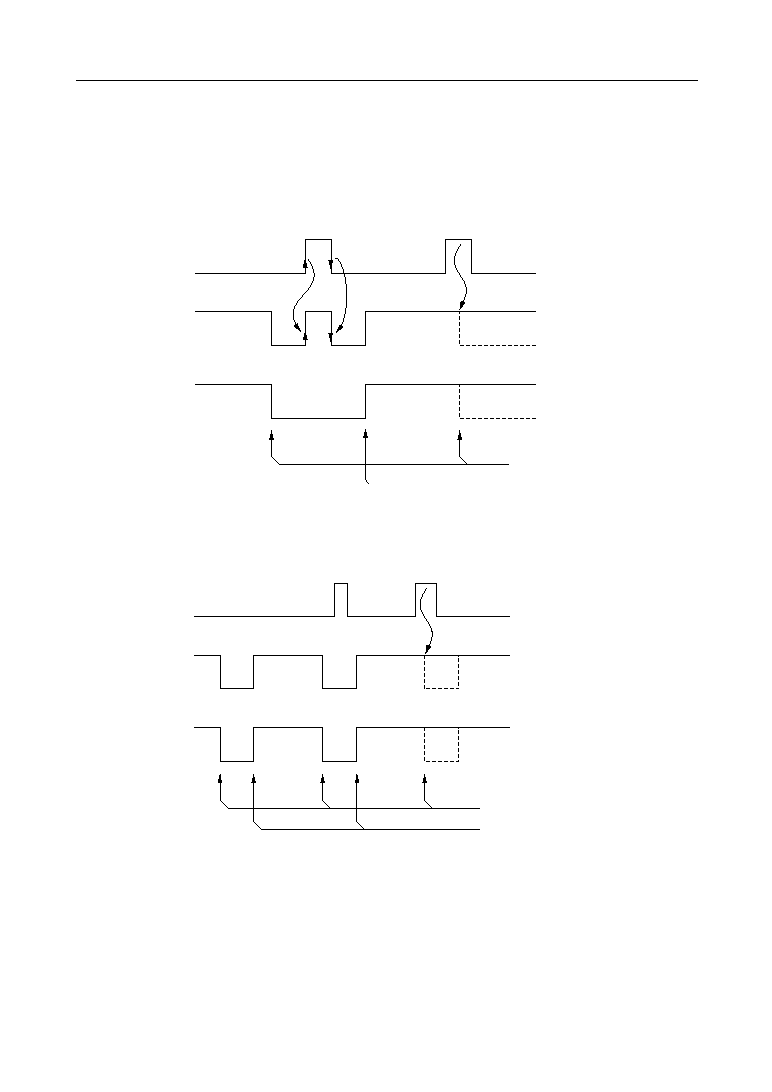
t
0
Period
0
1
0
1
The duration that the periodic waveform output is at "L" level is about 7.8ms.
t
1
and t
0
determine the output timing of the STD.P output.
e.g.) When t
1
="1", t
0
="1", MASK="0"
High impedance
12:00PM
STD.P output
when INT/STND="0"
STD.P output
when INT/STND="1"
"L" level
High impedance
"L" level
1:00PM
When writing into the 30-sec ADJ bit, a carry can occur.
Therfore, if (t
1
, t
0
) = (1, 0), (1, 1), the STD.P output may sometime be at "L" level. When INT/
STND="0", this "L" level is kept for a maximum of 9.8ms after under-second digits in 30-sec
ADJ is cleared (the 30-sec ADJ flag returns to "0").
If the selected interrupt period is 1 second, 1 minute, or 1 hour, and if a carry occurs during the
time the S
1
, S
10
, MI
1
, MI
10
registers are overwritten using the HOLD bit, and if data written
in these registers determines the interrupt timing set by the carry, the STD.P output will go to "L"
level after HOLD="0". (IRQ-F will is set to "1")
In other cases, writing to the S
1
, S
10
, MI
1
, MI
10
, H
1
registers do not change the STD.P output.
∑ INT/STND (interrupt-to-Standard waveform switching bit)
INT/STND = "1" : "1" of the IRQ-F bit and "L" level on the STD.P output are kept until IRQ-
F (C
D
register) is read out.
INT/STND = "0" : "1" of the IRQ-F bit returns to "0" after a certain time elapses (after about
7.8ms) or when IRQ-F is read out.
"L" level on the STD.P output returns to high impedance after a certain
time elapses.
130
° Semiconductor
MSM6782-01
∑ MASK
"1" of the MASK bit inhibits the setting of "1" to the IRQ-F flag and sets the STD.P output to
the high impedance state.
Interrupt mode (INT/STND="1")
IRQ-F
"1"
"0"
STD.P output
High impedance
"L" level
MASK bit
"1"
"1"
"0"
"0"
No interrupt is generated because
of MASK bit="1".
Interrupt timing
IRQ-F is read out.
Periodic timing waveform output mode (INT/STND="0")
"1"
"0"
STD.P output
High impedance
"L" level
MASK bit
"1"
"1"
"0"
"0"
No "L" level is output because
of MASK bit ="1".
Output timing
IRQ-F
Auto-return
(duration of "L" is about 7.8ms)
When the IRQ-F bit is read out before auto-return, the IRQ-F bit goes to "0", and the STD.P
output keeps "L" level for about 7.8ms, then goes into the high impedance state.

131
MSM6782-01
° Semiconductor
C
F
REGISTER (Control F Register)
∑ TEST
The TEST bit is used for testing by OKI and should be set to "0".
This bit can be cleared to "0" by setting the CE pin to "L" level.
∑ 24/12
This bit is used to switch between 24-hour system and 12-hour system.
24/12 = "1" : 24-hour system without PM/AM
24/12 = "0" : 12-hour system with PM/AM
When the 24/12 bit is overwritten, data in the H
1
~ W registers may become undefined.
Therefore, it is required to newly set those registers again.
∑ STOP
"1" of this bit stops clocking and "0" restarts clocking.
∑ REST
"1" of this bit clears under-second-time to zero and at the same time stops clocking. "0" of
this bit restarts clocking.
Take care not to set the TEST bit to "1" when writing "0" into the REST bit.
132
° Semiconductor
MSM6782-01
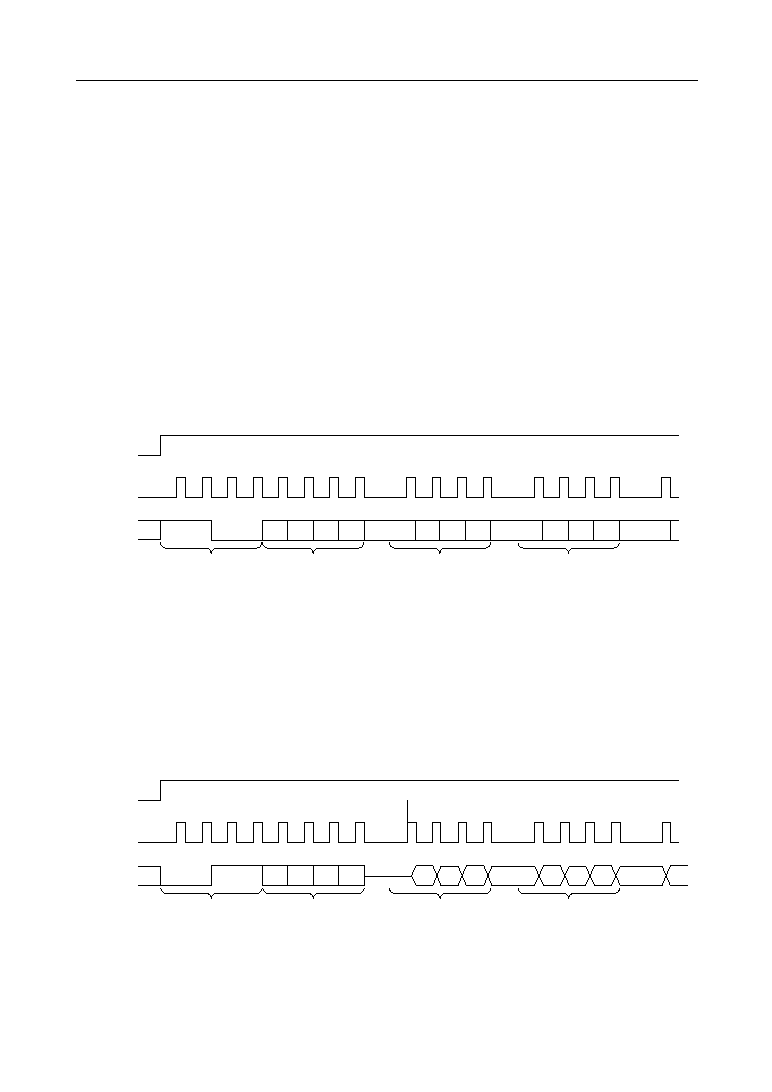
Usage
Functional Description
Writing and reading are executed in units of 4 bits after the CE input goes high. If the CE input
goes low before 4-bit data input is complete, the 4-bit data written when the CE input goes low
is ignored. (Data written before the CE input goes low is valid)
Writing and reading are executed starting from the LSB.
(WRITE)
1) The first 4 bits that are input after the CE input goes high are specified as "3" indicating the
WRITE mode. The address to be written is set into the second 4 bits.
2) The third 4 bits are written into the previously-set address.
The following 4-bit data are sequentially written into automatically-incremented addresses.
3) The address is automatically incremented in a loop way where address F is followed by
address 0.
(READ)
1) The first 4 bits that are input after the CE input goes high are specified as "C" indicating the
READ mode.
The address to be read is set into the second 4 bits.
2) The third 4-bit data is read from the previously-set address.
The following 4-bit data are sequentially read from automatically incremented addresses.
3) The address is automatically incremented in a loop way where address F is followed by
address 0.
WRITE mode
setting code
ÿ
D0
CE
CLK
I/O
ÿ
ÿ
ÿ
ÿ
ÿ
ÿ
ÿ
ÿ
ÿ
ÿ
ÿ
ÿ
ÿ
ÿ
ÿ
ÿ
D1 D2 D3 D0 D1 D2 D3
D0 D1 D2 D3
D0 D1 D2 D3
D0
Setting address
(N)
Data WRITE
address(N)
Data WRITE
address(N+1)
If a character other than "C" or "3" is specified to the mode setting code, the following data
is ignored and the DATA I/O pin keeps the input state.
READ mode
setting code
ÿ
D0
CE
CLK
I/O
ÿ
ÿ
ÿ
ÿ
ÿ
ÿ
ÿ
ÿ
ÿ
ÿ
ÿ
ÿ
ÿ
ÿ
ÿ
ÿ
D1 D2 D3 D0 D1 D2 D3
D0 D1 D2 D3
D0 D1 D2 D3
D
Setting address
(N)
Data READ
address(N)
Data READ
address(N+1)
The LSI is in the output mode.
∆
133
MSM6782-01
° Semiconductor
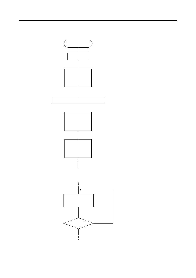
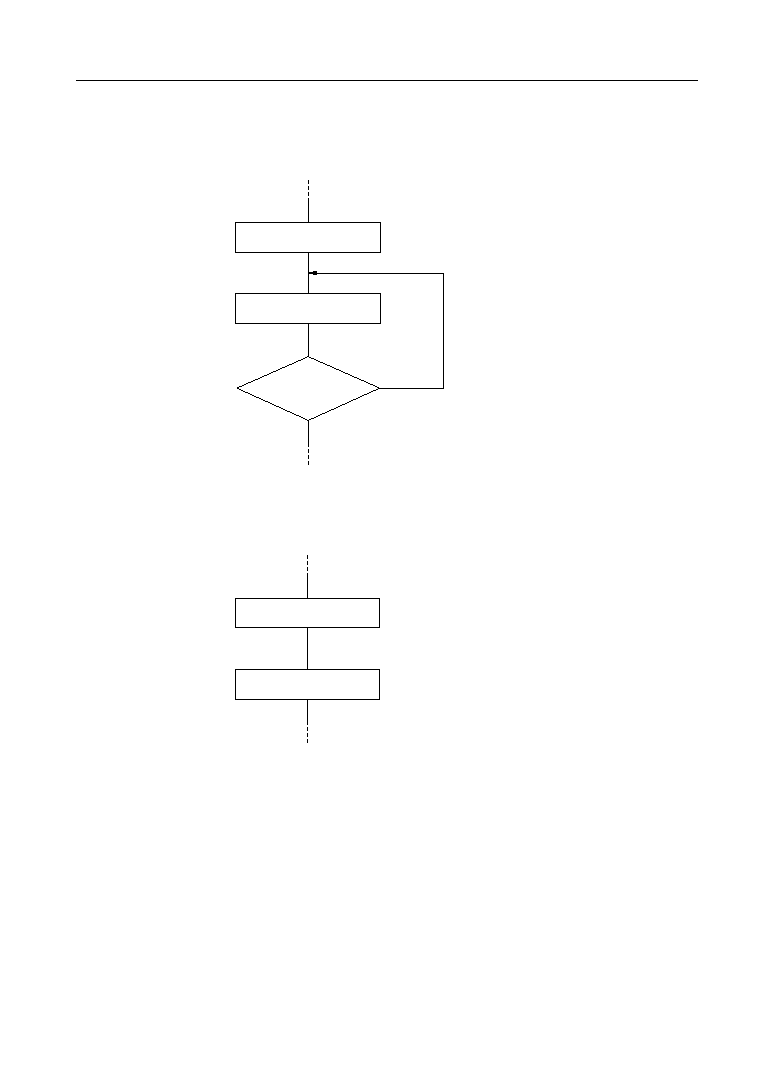
Power Supply
Reading of registers S
1
~ W
Note 1)
Data in registers C
D
, C
E
, C
F
, or registers S1 to W which are used as RAM can be read
out without using fr.
Note 2)
Checking fr is complete by checking only the last digit of fr which has been read out.
Power ON
Start
Clock starts
TEST ® 0
24/12 ® *1
STOP ® 1
REST ® 1
Write data into registers S1 - W
TEST ® 0
24/12 ® *1
STOP ® 0
REST ® 0
30-sec.ADJ ® 0
IRQ-F ® 0
CAL/HW ® *2
HOLD ® 0
∑ When the power is turned ON, all registers
and the STD.P output are undefined.
*1 = "0" OR "1"
*2 = "0" OR "1"
Y
Reading data from
registers S1 - W
f
r
= 0
N
134
° Semiconductor
MSM6782-01
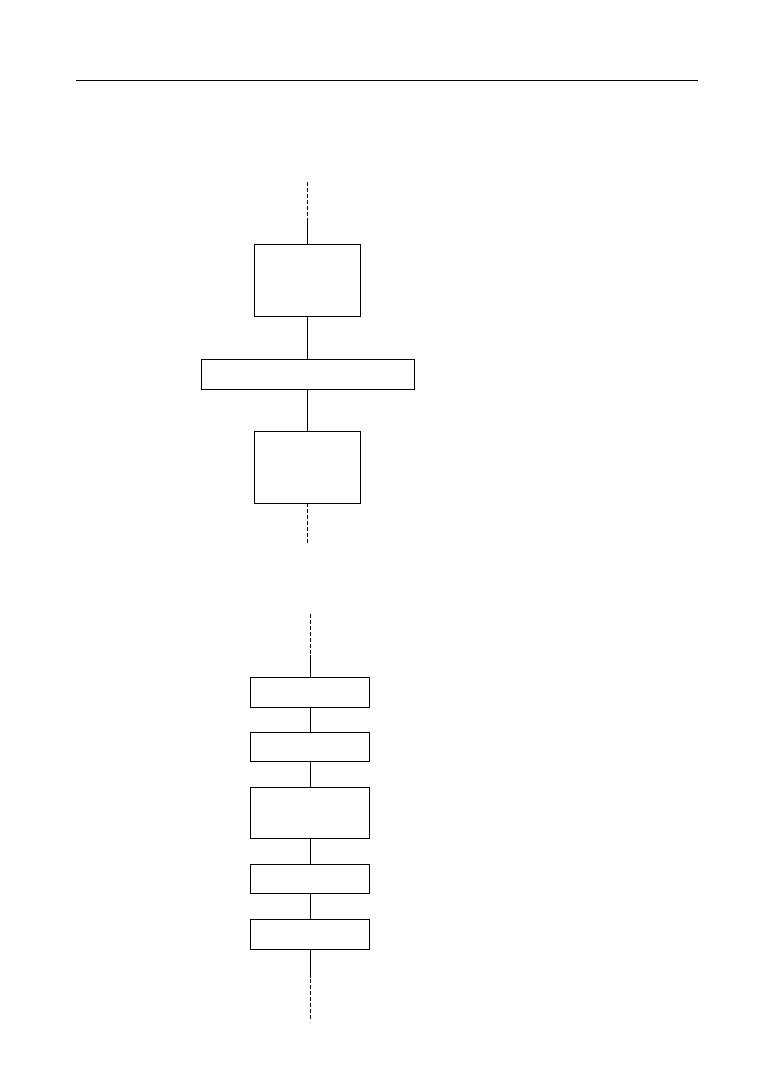
Writing data to S
1
- W
Method 1 : When under-second data is not stored
Method 2 : When under-second data is stored ( This method is used for switching summer time).
Clock starts
TEST ® 0
24/12 ® *1
STOP ® 1
REST ® 1
Write data into S1 ~ W
TEST ® 0
24/12 ® *1
STOP ® 0
REST ® 0
*1 = "0" OR "1"
All the operations must be finished within 1 second.
Otherwise, seconds may be lost.
Write data into
S1 ~ W
HOLD ® 1
100ms WAIT
HOLD ® 0
200ms WAIT
135
MSM6782-01
° Semiconductor
Writing 30-sec ADJ bit
Method 1
Y
30-sec ADJ = 0
N
Read 30-sec ADJ bit
30-sec ADJ ® 1
Method 2
125ms WAIT
30-sec ADJ ® 1
136
° Semiconductor
MSM6782-01
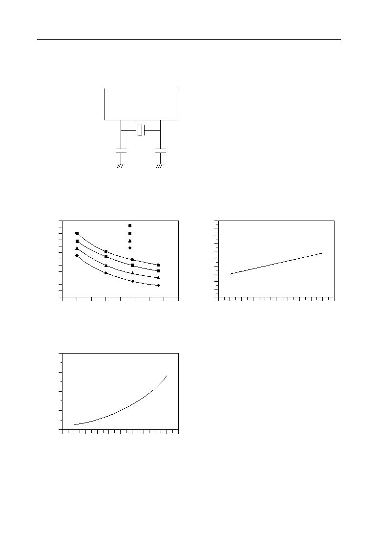
REFERENCE DATA
XT
XT
MSM6782-01
Crystal quartz : Citizen-made CFS-308
C
G
C
D
C
G
= 18pF
C
D
= 18pF
Capacitance dependency of oscillation frequency
60
40
20
0
≠20
≠40
≠60
D
f/f(ppm)
0
10
20
30
40
C
G
(pF)
C
D
= 15pF
C
D
= 18pF
C
D
= 24pF
C
D
= 33pF
Supply voltage dependency of oscillation frequency
10
0
≠10
D
f/f(ppm)
2
4
5
6
V
DD
(V)
3
Supply voltage dependency of I
DD
20
10
0
I
DD
(
m
A)
2
4
5
6
V
DD
(V)
3