 | –≠–ª–µ–∫—Ç—Ä–æ–Ω–Ω—ã–π –∫–æ–º–ø–æ–Ω–µ–Ω—Ç: MSM6786 | –°–∫–∞—á–∞—Ç—å:  PDF PDF  ZIP ZIP |

° Semiconductor
MSM6786
1/17
FEDL6786-03
° Semiconductor
MSM6786
1/3, 1/4 DUTY LCD DRIVER WITH 4-DOT COMMON DRIVER AND 29-DOT SEGMENT DRIVER
GENERAL DESCRIPTION
The MSM6786 is a dynamic display LCD driver and can be switched to 1/3 or 1/4 duty. It can
dis-play up to 116 segments with 1/4 duty and up to 87 segments with 1/3 duty. It can also drive
one LED directly. The built-in 5•6 key circuit allows input through a keyboard, and minimizes
the number of wires between the front panel and CPU.
FEATURES
∑ Power suppy voltage
: 5V
±
10%
∑ Operating temperature
: ≠40 to +85
∞
C
∑ 29-output segment driver
1/4 duty dynamic drive
: Up to 116 segments can be displayed
1/3 duty dynamic drive
: Up to 87 segments can be displayed
∑ One LED can be driven directly (I
O
=≠15mA max)
∑ Built-in 5•6 key scan circuit allows reading of the operation status of up to 30 switches.
∑ Interface with CPU is implemented by LOAD, DATA I/O and CLOCK in serial method.
∑ Built-in RC oscillator for LCD AC drive
∑ Built-in voltage dividing resistor for bias voltage generation
∑ Package:
56-pin plastic QFP (QFP56-P-910-0.65-2K) (Product name : MSM6786GS-2K)
FEDL6786-03
This version: Sep. 2000
Previous version: Nov. 1997
° Semiconductor
MSM6786
2/17
FEDL6786-03
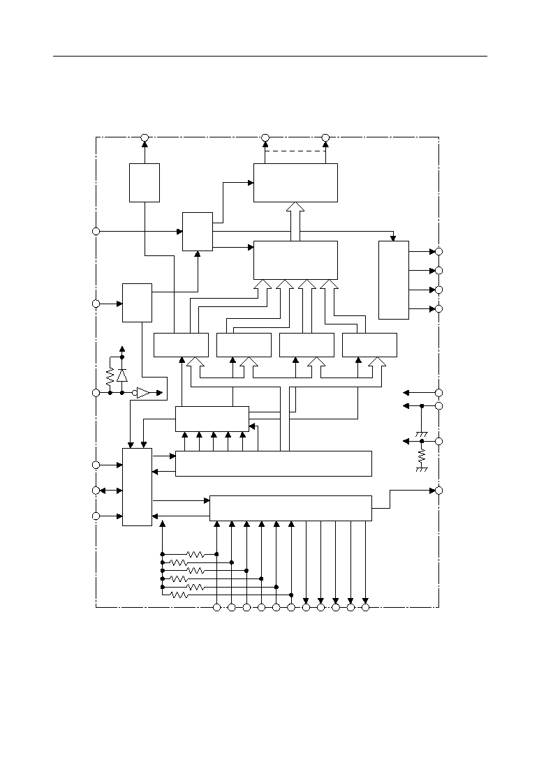
BLOCK DIAGRAM
3/4SEL
OSC
RESET
LED
DRV.
TIMING
GEN.
29-DOT SEG. DRV.
OSC
LOAD
CON-
TROL
LOGIC
DATA I/O
CLOCK
INT
5•6
KEY SCANNER
MODE
SELECTOR
(DATA LATCH1)
30-BIT LATCH
(DATA LATCH4)
29-BIT LATCH
(DATA LATCH2)
29-BIT LATCH
(DATA LATCH3)
29-BIT LATCH
COM.
DRV.
COM1
COM2
COM3
COM4
LED
SEG1
SEG29
V
DD
V
SS
TEST
C0 C1 C2 C3 C4 C5 R0 R1 R2 R3 R4
C5 C4 C3 C2 C1 C0
36(30+6)-BIT SHIFT REGISTER
29-BIT
DATA SELECTOR
V
DD
V
DD
° Semiconductor
MSM6786
3/17
FEDL6786-03
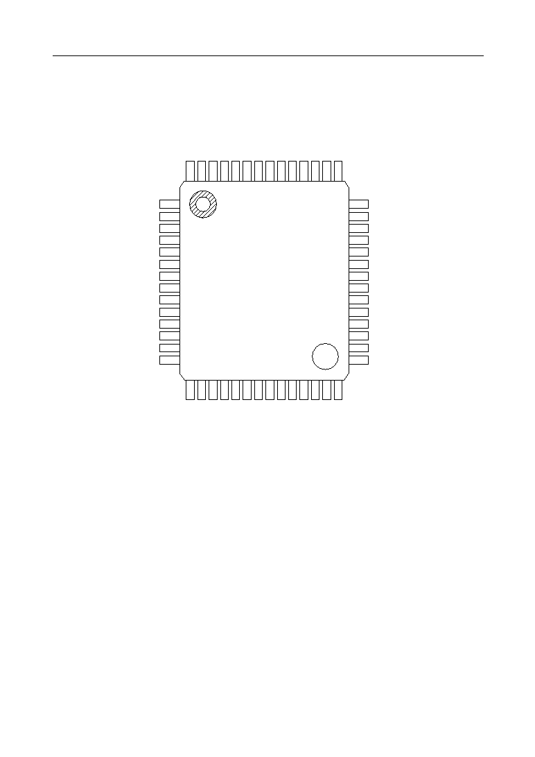
PIN CONFIGURATION (TOP VIEW)
14
13
12
11
10
9
8
7
6
5
4
3
2
1
29
30
31
32
33
34
35
36
37
38
39
40
41
42
SEG14
SEG13
SEG12
SEG11
SEG10
SEG9
SEG8
SEG7
SEG6
SEG5
SEG4
SEG3
SEG2
SEG1
SEG28
SEG29
C0
C1
C2
C3
C4
C5
R0
R1
R2
R3
R4
LOAD
28
27
26
25
24
23
22
21
20
19
18
17
16
15
SEG27
SEG26
SEG25
SEG24
SEG23
SEG22
SEG21
V
DD
SEG20
SEG19
SEG18
SEG17
SEG16
SEG15
43
44
45
46
47
48
49
50
51
52
53
54
55
56
CLOCK
DATAI/O
INT
RESET
LED
3/4SEL
V
DD
OSC
V
SS
TEST
COM4
COM3
COM2
COM1
56-Pin Plastic QFP

° Semiconductor
MSM6786
4/17
FEDL6786-03
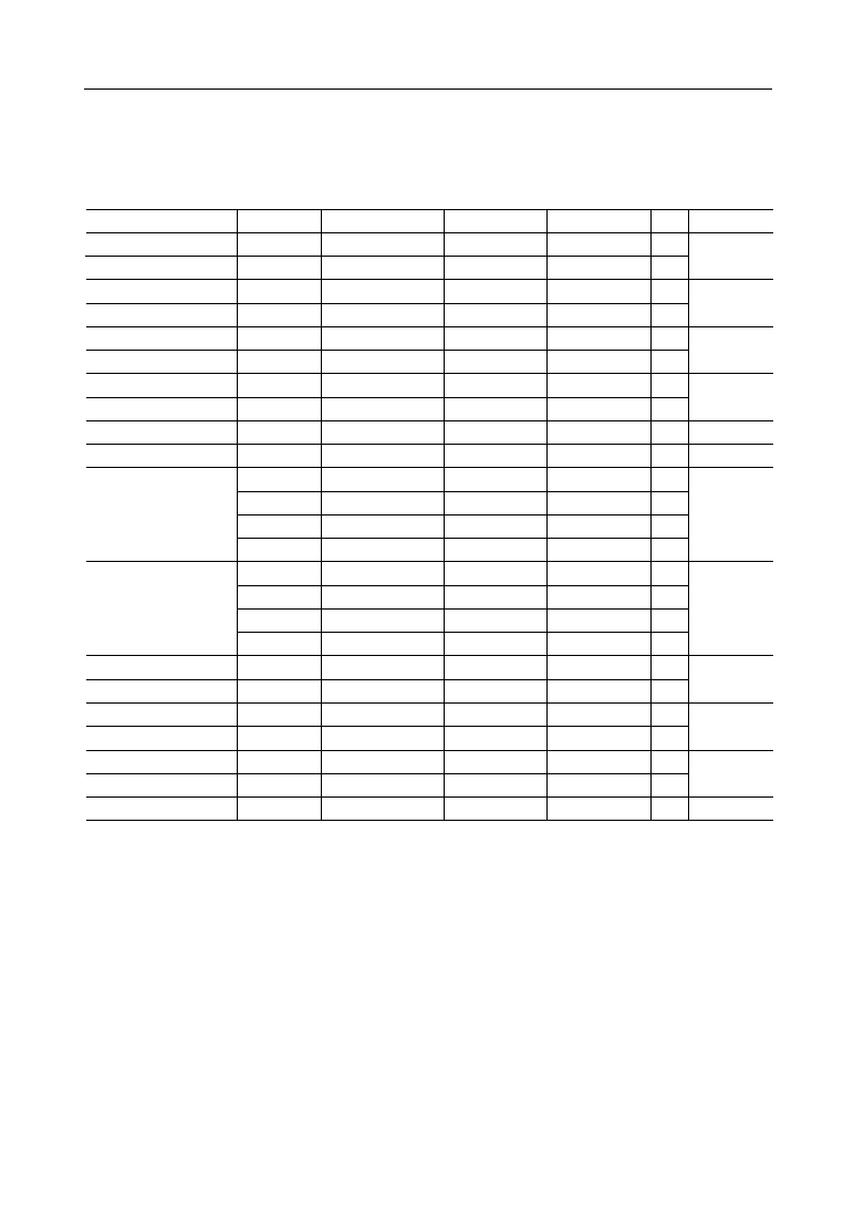
ABSOLUTE MAXIMUM RATINGS
*1 Applied to LED output
RECOMMENDED OPERATING CONDITIONS
Parameter
Symbol
Condition
Range
Unit
V
DD
V
SS
=OV
4.5 to 5.5
V
T
op
--
≠40 to +85
∞
C
Power Supply Voltage
Operating Temperature
Specifications of External Parts (oscillation circuit)
Parameter
Symbol
Condition
Unit
R
O
--
kW
C
O
--
mF
Oscillation Resistor (Resistance)
Oscillation Capacitor (Capacitance)
Max.
82
0.047
Min.
20
0.01
Parameter
Symbol
Condition
Rating
Unit
V
DD
Ta=+25
∞
C
≠0.3 to +6.5
V
V
I
Ta=+25
∞
C
≠0.3 to V
DD
+0.3
V
I
O
Ta=+25
∞
C
≠20
mA
T
STG
--
≠55 to +150
∞
C
Power Supply Voltage
Input Voltage
Output Current
Storage Temperature
*1
° Semiconductor
MSM6786
5/17
FEDL6786-03
ELECTRICAL CHARACTERISTICS
DC Characteristics
*1 CLOCK, LOAD, DATA I/O, RESET and 3/4SEL
*2 C
O
= 0.022 mF, R
O
= 33 kW, no load
Parameter
Symbol
Condition
Applied Pin
Min.
Max.
Unit
"H" Input Voltage
"L" Input Voltage
"H" Input Voltage
"L" Input Voltage
"H" Input Current
"L" Input Current
"H" Input Current
"L" Input Current
"L" Input Current
"L" Input Current
"H" Output Voltage
"L" Output Voltage
"H" Output Voltage
"L" Output Voltage
"H" Output Voltage
"L" Output Voltage
Supply Current
V
IH1
--
*1
0.8V
DD
V
V
IL1
V
IH2
V
IL2
I
IH1
I
IL1
I
IH2
I
IL2
I
IL3
I
IL4
V
OS0
V
OS1
V
OS2
V
OS3
V
OC0
V
OC1
V
OC2
V
OC3
V
OH1
V
OL1
V
OH2
V
OL2
V
OH3
V
OL3
I
DD
Segment Output
Voltage
Common Output
Voltage
--
--
--
V
I
=V
DD
V
I
=0V
V
I
=V
DD
V
I
=0V
V
DD
=5.0V, V
I
=0V
V
DD
=5.0V, V
I
=0V
I
O
=≠10mA
I
O
=
±
10mA
I
O
=
±
10mA
I
O
=10mA
I
O
=≠10mA
I
O
=
±
10mA
I
O
=
±
10mA
I
O
=10mA
I
O
=≠15mA
I
O
=0.1mA
I
O
=≠0.4mA
I
O
=0.4mA
I
O
=≠50mA
I
O
=1.0mA
*2
0
0.7V
DD
0
--
--
--
--
≠0.07
≠0.009
V
DD
≠0.8
2/3V
DD
≠0.8
1/3V
DD
≠0.8
--
V
DD
≠0.77
2/3V
DD
≠0.77
1/3V
DD
≠0.77
--
V
DD
≠1.5
--
V
DD
≠0.4
--
2.5
--
--
V
DD
0.2V
DD
V
DD
0.3V
DD
1
≠1
10
≠10
≠0.36
≠0.045
--
2/3V
DD
+0.8
1/3V
DD
+0.8
0.8
--
2/3V
DD
+0.77
1/3V
DD
+0.77
0.77
--
0.4
--
0.4
--
0.4
0.4
V
V
V
mA
mA
mA
mA
mA
mA
V
V
V
V
V
V
V
V
V
V
V
V
V
V
mA
C0-C5
CLOCK, LOAD
3/4SEL
DATA I/O
C0-C5
RESET
SEG1-SEG29
COM1-COM4
LED
DATA I/O
INT
R0-R4
V
DD
(V
DD
=5V
±
10%, Ta=≠40 to +85
∞
C)
° Semiconductor
MSM6786
6/17
FEDL6786-03
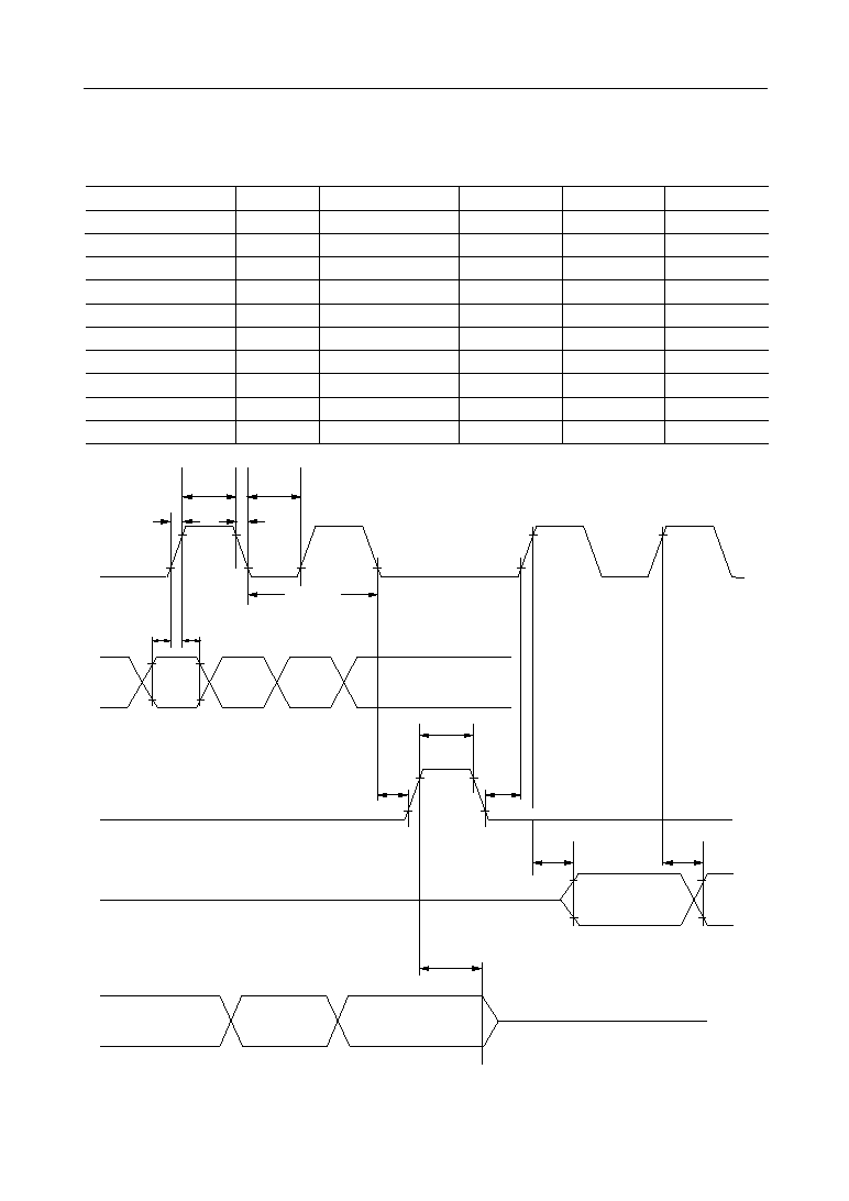
Switching Characteristics
LOAD
t
r
DATA I/O
(When changing from input mode to output mode)
DATA I/O
(When changing from output mode to input mode)
t
WCP
t
WCP
t
f
0.8V
DD
0.2V
DD
1/f
CP
0.8V
DD
0.2V
DD
t
LC
t
WLD
t
CL
0.8V
DD
t
PD1
t
PD1
0.8V
DD
0.2V
DD
0.2V
DD
HiZ
t
PD2
HiZ
0.8V
DD
0.2V
DD
t
DSU
t
DHD
CLOCK
DATA I/O
(During input mode)
(The charging and discharging time during high impedance depends on trace resistance and stray capacitance.)
Parameter
Symbol
Condition
Min.
Max.
Unit
Clock Frequency
Clock Pulse Width
Rise/Fall Time
Data Setup Time
Data Hold Time
Load Pulse Width
Clock∆Load Time
Load∆Clock Time
Output Delay Time 1
Output Delay Time 2
f
CP
--
--
MHz
t
WCP
t
r
,t
f
t
DSU
t
DHD
t
WLD
t
CL
t
LC
t
PD1
t
PD2
--
--
--
200
--
100
100
200
100
200
--
--
2.0
--
50
--
--
--
--
--
300
300
ns
ns
ns
ns
ns
ns
ns
ns
ns
--
--
--
--
C
L
=50pF
--
(V
DD
=5V
±
10%, Ta=≠40 to +85
∞
C)

° Semiconductor
MSM6786
7/17
FEDL6786-03
FUNCTIONAL DESCRIPTION
Pin Functional Description
OSC (Pin 50)
This is an input/output pin for the oscillator to generate LCD AC lighting and keyscan pulses.
Connect an external capacitor and resistor as shown below to form an RC oscillation circuit.
The relationship between frame frequency f
FRM
, keyscan period T
SCN
and oscillation frequency
f
OSC
is:
f
FRM
= f
OSC
/24, T
SCN
= 20/f
OSC
DATA I/O (Pin 44)
This is a serial data input/output pin. The pin is in output state from the first shift clock rise after
key data output command writing, to the load pulse rise, and in input state otherwise. (The
pin is in input state during reset.)
The relationship between the data levels of this pin and the operations is shown below.
Level
Display
Key Status
"H"
ON
ON (close)
"L"
OFF
OFF (open)
CLOCK (Pin 43)
This is an input pin for the shift clock. DATA I/O pin data is either input or output in
synchroniza-tion with each rising clock edge.
LOAD (Pin 42)
This is a load pulse input pin used to transfer serial input data to a latch for display, to write
commands, or to release the DATA I/O pin in output state.
C
O
OSC
R
O
V
DD

° Semiconductor
MSM6786
8/17
FEDL6786-03
R0 ≠ R4 (Pin 37-Pin 41)
These are key switch scan pulse output pins. During the scan operating, "L" level is output in
sequence. All pluses go to "L" level when scanning stops.
C0 ≠ C5 (Pin 31-Pin 36)
These are input pins that detect the key status. These pins have pull-up resistors. Key matrices
are formed with pins R0 ≠ R4.
C0
C1
C2
C3
C4
C5
R0 R1 R2 R3 R4
INT (Pin 45)
This is the keyscan end signal output pin. This pin becomes "H" when one scan cycle is
completed, and returns to "L" by a load pulse after data output or when the "Scan Stop"
command is written. (The pin is in "L" status during reset.)
If this pin is not used, leave it unconnected.

° Semiconductor
MSM6786
9/17
FEDL6786-03
RESET (Pin 46)
This is a reset signal input pin that intializes the IC, and is activated at "L" level. This pin has
an internal pull-up resistor. The power ON reset usually operates by externally connecting a
capacitor.
SEG1 ≠ SEG29 (Pin 1-Pin 20, Pin 22-Pin 30)
These are the output pins for LCD, and are connected to the segment pins of the LCD panel. See
the section on data configuration for the relationship between SEG output and input data.
COM1 ≠ COM4 (Pin 56-Pin53)
These are output pins for the LCD, and are connected to common pins of the LCD panel. When
1/3 duty is selected, COM4 pin should be left unconnected. See the section on data configuration
of common output and input data.
LED (Pin 47)
This is an output pin for the LED drive. The LED and current limiting resistor are externally
connected.
RESET
V
DD
C
RST
LED
3/4SEL (Pin 48)
This is a duty select input pin. When "H" level is input, 1/3 duty is selected and when "L" level
is input, 1/4 duty is selected.
TEST (Pin 52)
This is an input pin for IC testing. This pin should be connected to V
SS.
V
DD
, V
SS
(Pin 21, 49, 51)
These are power voltage supply and ground pins.

° Semiconductor
MSM6786
10/17
FEDL6786-03
Operating Description
Display data input
As shown in the section on data configuration, the data for display consists of data fields that
correspond to segment ON/OFF and command fields which indicate display data input.
Set the bits C0 to C1 of the command field to "0" or "1" according to the common to which the
display data corresponds. To the other four bits, set the display data input commands. LED
display data corresponds to common 1. Data input to the DATA I/O pin is saved in a shift
register at the rising edge of the CLOCK pulse, and is transferred to a data latch for display while
the LOAD pulse is at "H" level, and is then output through a segment driver.
Key data output
The state of a key switch is indicated by ON = 1, OFF = 0, and is read as 30 bits serial data. (For
information on the sequence, see the section on data configuration.) To output data, the output
command must be written, which causes the data to be output in synchronization with the rising
edge of the CLOCK pulse. By inputting a LOAD pulse after that, the DATA I/O pin returns to
the input state, and the next data or command can be input. (If a LOAD pulse is applied earlier
than the 30th data, the key data is output only by the number of the CLOCK pulse. If CLOCK
pulses more than 30 data bits are applied, 30 data bits of key data are circulated.)
D1
D2
D3
D4
D28 D29 D30
C0
C1
C2
C3
C4
CLOCK
DATAI/O
Old Data
New Data
LOAD
Display Output
C5
C3
C4
C5
O1
O2
O3
O29
O30
CLOCK
DATAI/O
Next Command
Input
LOAD
Output Command Write
Key Data Read
Note1 : The last key data must be read before the LOAD pulse rises.
Note2 : Upon swiching from output mode to input mode, the state of the DATA I/O pin is
unstable for the duration of 300 ns after the rising of LOAD pulse. For this reason, never
input data to the DATA I/O pin during this period.

° Semiconductor
MSM6786
11/17
FEDL6786-03
R0
R1
R2
R3
R4
Scan Start Command Write
or Key Status Changed
T
SCN
Data Read
Data Read
Data Read
Scan Stop Command
Write
INT
Keyscan
Keyscan starts when the key state is changed or when the "Keyscan Start" command is written.
Scan continues until the "Keyscan Stop" command is written. (When powered on, the power-
ON reset sets at scan stop state.)
When 1 keyscan cycle (T
SCN
) ends, the INT signal becomes "H", so this signal can be used as an
interrupt flag, which is dependent on switching conditions of keys. The INT signal is reset when
either the LOAD pulse is input after key data is output, when the "Keyscan Stop" command is
set, or when a reset signal is applied.
Notes : 1. A recognition error may occur if 3 or more key switches are pressed at the same time.
(A switch that was not pressed is recognized as being pressed.) To properly
recognize 3 or more key switches as being pressed at the same time, serially insert
diodes at each switch. In order not to recognize 3 or more key switches as being
pressed at the same time, a possible approach is to program the software so that the
read data will be ignored when there are 3 or more ones in the data.
The device recognizes simultaneous pressing of 2 key switches. However, take Note
2 into consideration.
2. A change of key state is detected as a change in column input (C0 - C5). Therefore
even if multiple switches connected to the same column are pressed at the same time,
nothing will be detected as a change.

° Semiconductor
MSM6786
12/17
FEDL6786-03
Display on, Display off
In power ON reset state, display will go out. To turn the display on, write the display ON
command. The display and LED can go out by writing the display OFF command, irrespective
of display data.
Display ON command releases the display OFF state. By writing this command, display will
return to original state.
D1 D2
C4
C2
C3
C4
C5
C2
C3
C4 C5
CLOCK
DATAI/O
LOAD
Display On/Off
C5
Display On
Command Write
Display Off
Command Write
RESET
Display Data Input
Command List
Command Name C5 C4 C3 C2 C1 C0
Operation
F1
F2
F3
F4
F5
F6
F7
F8
0
0
1
0
0
0
1
0
1
1
0
1
0
•
•
•
0
1
1
0
0
0
1
0
1
1
1
0
1
0
•
•
1
0
1
1
•
•
1
1
0
•
•
•
1
0
0
•
•
•
1
1
1
•
•
•
Display Data Input (Corresponding to Common 1)
Display Data Input (Corresponding to Common 2)
Display Data Input (Corresponding to Common 3)
Display Data Input (Corresponding to Common 4)
Key Data Output
Display Data Input (1) + Key Data Output
Display Data Input (2) + Key Data Output
Display Data Input (3) + Key Data Output
Display Data Input (4) + Key Data Output
Display Off
Display On
Key Scan Stop + Key Data Output
Key Scan Stop
Key Scan Start + Key Data Output
• : Don't care

° Semiconductor
MSM6786
13/17
FEDL6786-03
Data Configuration
(Input data)
D30
D29
D28
D3
D2
D1
C0
C1
C2
C3
C4
C5
Command
LCD Display Data
LED Display Data
Corresponds to SEG1
Corresponds to SEG29
First Bit
Notes : 1. LED data corresponds to common 1 side (C0, C1 = 0).
2. D1 bit is unnecessary when LED output is not used.
3. Data output commands F2, F6 ≠ F8 become effective if at least 3 bits (C3 ≠ C5) are
input. (D1 ≠ D30 and C0 ≠ C2 bits are not necessary.)
Command F4 and command F5 become effective if at least 4 bits (C2 - C5) are input.
(D1 - D30, C0 and C1 bits are not necessary.)
4 . If dummy bits are necessary, add them before first bit.
(Output data)
C5 C4 C3 C2 C1 C0 C5 C4 C3 C2 C1 C0 C5 C4 C3 C2 C1 C0 C5 C4 C3 C2 C1 C0 C5 C4 C3 C2 C1 C0
R4
R3
R2
R1
R0
30
1
Last Bit
First Bit

° Semiconductor
MSM6786
14/17
FEDL6786-03
APPLICATION CIRCUIT
COM3
COM4
COM4
LED
COM3
V
DD
LOAD
DATAI/O
CLOCK
INT
SEG1
SEG29
MSM6786
+5V
C0
OSC
V
SS
TEST
RESET
SEG1
SEG29
1/4 duty LCD Panel
C1 C2 C3 C4 C5
R0 R1 R2 R3 R4
CPU
5•6 Key Matrix
COM1
COM2
COM2
COM1
3/4SEL

° Semiconductor
MSM6786
15/17
FEDL6786-03
REFERENCE DATA
Resistance R
O
[kW]
f
FRM
vs. R
O
, C
O
1000
400
300
200
100
70
50
30
20
10
20
40
60
80
100
1
Frame frequency Characteristics
The scanning period T
SCN
is defined by the following equation:
T
SCN
=
5
6f
FRM
[ms]
Frame Frequency f
FRM
[Hz]
T
a
= 25 [
∞
C]
V
DD
= 5.0 [V]
C
O
= 0.01
µ
F
C
O
= 0.022
µ
F
C
O
= 0.033
µ
F
=
20
f
OSC
[ms]
91

° Semiconductor
MSM6786
16/17
FEDL6786-03
(Unit : mm)
PACKAGE DIMENSIONS
Notes for Mounting the Surface Mount Type Package
The SOP, QFP, TSOP, SOJ, QFJ (PLCC), SHP and BGA are surface mount type packages, which
are very susceptible to heat in reflow mounting and humidity absorbed in storage.
Therefore, before you perform reflow mounting, contact Oki's responsible sales person for the
product name, package name, pin number, package code and desired mounting conditions
(reflow method, temperature and times).
Package material
Lead frame material
Pin treatment
Package weight (g)
Oki Electric Industry Co., Ltd.
Rev. No./Last Revised
Epoxy resin
42 alloy
Solder plating (5 mm)
0.43 TYP.
4/Nov. 28, 1996
QFP56-P-910-0.65-2K
Mirror finish
.

° Semiconductor
MSM6786
17/17
FEDL6786-03
NOTICE
1.
The information contained herein can change without notice owing to product and/or
technical improvements. Before using the product, please make sure that the information
being referred to is up-to-date.
2.
The outline of action and examples for application circuits described herein have been
chosen as an explanation for the standard action and performance of the product. When
planning to use the product, please ensure that the external conditions are reflected in the
actual circuit, assembly, and program designs.
3.
When designing your product, please use our product below the specified maximum
ratings and within the specified operating ranges including, but not limited to, operating
voltage, power dissipation, and operating temperature.
4.
Oki assumes no responsibility or liability whatsoever for any failure or unusual or
unexpected operation resulting from misuse, neglect, improper installation, repair, alteration
or accident, improper handling, or unusual physical or electrical stress including, but not
limited to, exposure to parameters beyond the specified maximum ratings or operation
outside the specified operating range.
5.
Neither indemnity against nor license of a third party's industrial and intellectual property
right, etc. is granted by us in connection with the use of the product and/or the information
and drawings contained herein. No responsibility is assumed by us for any infringement
of a third party's right which may result from the use thereof.
6.
The products listed in this document are intended for use in general electronics equipment
for commercial applications (e.g., office automation, communication equipment,
measurement equipment, consumer electronics, etc.). These products are not authorized
for use in any system or application that requires special or enhanced quality and reliability
characteristics nor in any system or application where the failure of such system or
application may result in the loss or damage of property, or death or injury to humans.
Such applications include, but are not limited to, traffic and automotive equipment, safety
devices, aerospace equipment, nuclear power control, medical equipment, and life-support
systems.
7.
Certain products in this document may need government approval before they can be
exported to particular countries. The purchaser assumes the responsibility of determining
the legality of export of these products and will take appropriate and necessary steps at their
own expense for these.
8.
No part of the contents contained herein may be reprinted or reproduced without our prior
permission.
9.
MS-DOS is a registered trademark of Microsoft Corporation.
Copyright 2000 Oki Electric Industry Co., Ltd.
Printed in Japan