 | –≠–ª–µ–∫—Ç—Ä–æ–Ω–Ω—ã–π –∫–æ–º–ø–æ–Ω–µ–Ω—Ç: MSM6889RS | –°–∫–∞—á–∞—Ç—å:  PDF PDF  ZIP ZIP |

1/21
MSM6889
° Semiconductor
GENERAL DESCRIPTION
The MSM6889 is best suited to be used as a signal transmitter/receiver LSI for a telemetering
system that employs a no-ringing communication system.
The meter terminal of a telemetering system consists of this device, meter, NCU, and
communication controller.
The MSM6889 contains a PB tone detector, a call progress tone (CPT) detector, a PB tone
generator, and a 300-bps full-duplex modem conforming to ITU-T V.21.
FEATURES
∑ Power supply : +5 V
±
10%, +2.5 V or higher for digital interface.
∑ Power consumption
Operating mode : 9 mA Typ., 12 mA Max.
Power down mode : 0.1 mA Max.
∑ The operating mode can be selected from PB tone transmit, PB tone detect, and FSK modem
(answer/originate). The FSK modem cannot be operated concurrently with other functions.
Modem test modes are also available.
∑ The call progress tone (CPT) detector operates in PB tone transmit mode or in FSK modem
mode.
∑ PB receiver output is 3-state, and externally connectable to 4-bit input for PB tone generator
through the bus line.
∑ Modem transmit/receive data, carrier detect, request to send, and call progress tone detect
have their dedicated pins.
∑ Prefilter and smoothing filter are provided in analog input and output.
∑ On-chip 3.579545 MHz crystal oscillator
∑ 3.579545 MHz master clock output pin (CMOS compatible)
∑ Power down mode
∑ Modem : Conforms to ITU-T V.21 (300 bps, full-duplex)
∑ Transmit analog signals (modem signal, DTMF tone) : Level is independently adjustable
externally. Carrier detect level is also adjustable externally.
∑ Package options:
42-pin plastic DIP
(DIP42-P-600-2.54)
(Product name : MSM6889RS)
56-pin plastic QFP
(QFP56-P-1519-1.00-K) (Product name : MSM6889GS≠K)
E2A0027-16-X1
° Semiconductor
MSM6889
Multi-Function Telecommunication LSI
This version: Jan. 1998
Previous version: Nov. 1996
2/21
MSM6889
° Semiconductor
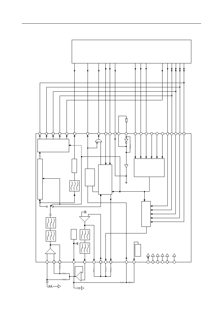
BLOCK DIAGRAM
AIN-
AIN+
GAR
2765 Hz
Pre-LPF
SG
AO
SMOOTH
+
-
+-
GAT2
GAT1
PB
MOD
VR2
VR1
SG
LPF
+
-
Vref
PON
VA
AG
VD
DG
VD2
Power ON
+5 V (A)
0 V (A)
+5 V (D)
0 V (D)
Digital Interface
PB Tone
Generator
PB-Tone Receiver
400 Hz
DET
TIMING
STATUS
I/O
CON-
TROL
Carrier
Detect
FSK Modem
MODE
SELECT
&
TEST
PB4
PB3
PB2
PB1
SP
CP
CD
RD
TD
RS
CLK
X2
X1
X'tal
3.58 MHz
*
*
*
MODE1
*
MODE2
*
MODE3
*
ICT1
*
ICT2
*
ICT3
*
TEN
*
PBG1
*
PBG2
*
PBG3
PBG4
Micro-
controller
Note) PB1 to PB4: 3-State Outputs
*With pull-up resistor
8
*
*

3/21
MSM6889
° Semiconductor
PIN CONFIGURATION (TOP VIEW)
42-Pin Plastic DIP
1
42
2
41
3
40
4
39
5
38
6
37
7
36
8
35
9
34
10
33
11
32
12
31
13
30
14
29
15
28
16
27
17
26
18
25
19
24
20
23
21
22
VA
GAR
AIN+
AIN≠
AO
SG
GAT1
GAT2
MOD
PB
VR1
VR2
AG
PBG1
PBG2
PBG3
PBG4
TEN
TD
RS
DG
VD
VD2
NC
PON
SP
PB4
PB3
PB2
PB1
CP
CD
RD
CLK
X2
X1
MODE3
MODE2
MODE1
ICT3
ICT2
ICT1
NC : No connect pin

4/21
MSM6889
° Semiconductor
56-Pin Plastic QFP
1
2
3
4
5
6
7
8
9
10
11
12
13
14
15
16
17
18
19
20
21
22
23
24
25
26
27
28
42
41
40
39
38
37
36
35
34
33
32
31
30
29
56
55
54
53
52
51
50
49
48
47
46
45
44
43
NC
PBG4
TEN
TD
NC
RS
DG
ICT1
ICT2
NC
ICT3
MODE1
MODE2
MODE3
NC
AO
AIN≠
AIN+
NC
GAR
NC
VA
VD
NC
VD2
PON
SP
NC
PBG3
NC
PBG2
PBG1
AG
VR2
VR1
NC
NC
PB
MOD
GAT2
GAT1
SG
NC
X1
X2
NC
CLK
RD
NC
CD
CP
NC
PB1
PB2
PB3
PB4
NC : No connect pin

5/21
MSM6889
° Semiconductor
PIN DESCRIPTION
+5 V Power Supply (Analog Circuit).
When power is turned on or the power down mode is released, the
device must be put into the PB tone transmit mode or PB tone
detect mode.
--
VA
35
1
Output, non-inverting input and inverting input pins of on-chip
operational amplifier.
No hybrid transformer is required by use of these pins. (See Fig. 2.)
O
GAR
37
2
I
AIN+
39
3
I
AIN≠
40
4
Analog signal output.
PB tone or modem transmit signal is output from this pin.
O
AO
41
5
On-chip signal ground, having a potential of about +2.5 V.
O
SG
43
6
I
GAT1
44
7
O
GAT2
45
8
O
MOD
46
9
O
PB
47
10
PB is the PB tone output and MOD is the modem signal output.
By connecting external resistors to GAT1 and GAT2 pins, signal level can
be set at required values for the modem signal and
the PB tone that are output from AO, independently. (See Fig. 3.)
These pins are used to externally adjust the received carrier
detect(CD) signal level.
The potential of VR1 to SG is about +1.1 V. The carrier
detect level can be set at the required value by a on-chip resistor
divider between VR1 and SG. The given potential to VR2 is set
about +0.88 V with high resistance inside the IC. (See Fig. 4.)
O
VR1
50
11
I
VR2
51
12
Analog Ground, 0 V.
--
AG
52
13
I*
PBG1
53
14
I*
PBG2
54
15
I*
PBG3
56
16
I*
PBG4
2
17
Inputs used to specify PB tone to be sent.
PB1 to PB4 can be connected externally like 4-bit bus line. Data is
latched at the falling edge of TEN. (See Fig. 7 and Fig. 8.)
Description
I/O
Name
Pin Number
GS
RS
* Digital input pulled up by a high resistance inside the IC.

6/21
MSM6889
° Semiconductor
PB tone transmit enable.
PBG1 to PBG4 data are latched at the falling edge of TEN, and PB
tone is generated at digital "0" level. (See Fig. 7.)
I*
TEN
3
18
Modem transmit serial data input.
Data stream less than 300 bps should be input.
Digital "1" and "0" correspond to "Mark" and "Space" respectively.
I*
TD
4
19
Request to send data input .
While RS is at digital "0" level, modem transmit is enabled.
I*
RS
6
20
Digital Ground, 0 V.
--
DG
7
21
I*
ICT2
9
23
I*
ICT3
11
24
Used to check performance characteristics of the IC.
Description
I/O
Name
Pin Number
GS
RS
Input used to select call progress tone (CPT) detect output
waveform. (See Fig. 9.)
I*
ICT1
8
22
Independent of operating mode. Leave these pins open.
I*
MODE1
12
25
I*
MODE2
13
26
Inputs used to specify operating mode.
(See Table 1.)
I*
MODE3
14
27
3.579545 MHz crystal resonator should be connected to X1 and X2.
When applying external clock to the device, it should be connected
to X2 through the AC coupling capacitor of 100 pF and X1 has to be
open.
I
X1
16
28
O
X2
17
29
3.579545 MHz clock output.
O
CLK
19
30
Modem receive serial data output.
Digital "1" and "0" correspond to "Mark" and "Space" respectively.
When CD (Carrier Detect) is off, RD is hold at "Mark" state.
Carrier Detect output.
Digital "0" and "1" represent "Detect" and "No-detect" respectively.
O
RD
20
31
O
CD
22
32
* Digital input pulled up by a high resistance inside the IC.

7/21
MSM6889
° Semiconductor
Call progress tone (CPT) detect output.
When a CPT is detected, the waveform selected by ICT1 is output.
(See Fig. 9. )
O
CP
23
33
Description
I/O
Name
Pin Number
GS
RS
O
PB2
26
35
O
PB3
27
36
Receive PB tone code outputs.
The output impedance of these pins becomes high except when the
device operates as PB tone receiver. (See Fig. 7 and Fig. 8. )
O
PB4
28
37
+5 V power supply (digital circuit).
When power is turned on or the power down mode is released, the
device must be put into the PB tone transmit mode or PB tone
detect mode.
--
VD
34
42
O
PB1
25
34
PB tone receive data present.
Digital "1" represents that this pin is receiving the PB tone.
(See Fig. 8. )
O
SP
30
38
I
PON
31
39
Power down mode select. Digital "1" on this pin puts the whole
circuit of the device into the power down state.
--
NC
--
40
No connection.
--
VD2
32
41
Power supply for digital interface output.
The supply voltage from +2.5 V to VD is possible for VD2. For
example, when the device interfaces to the MCU working on +3 V
supply, the +3 V supply has to be applied to the VD2 pin.
Note that this function is effective to all of digital output pins
except X1, X2, and CLK.
There is no restriction regarding the power supplies (VD and VD2)
applying procedure.

8/21
MSM6889
° Semiconductor
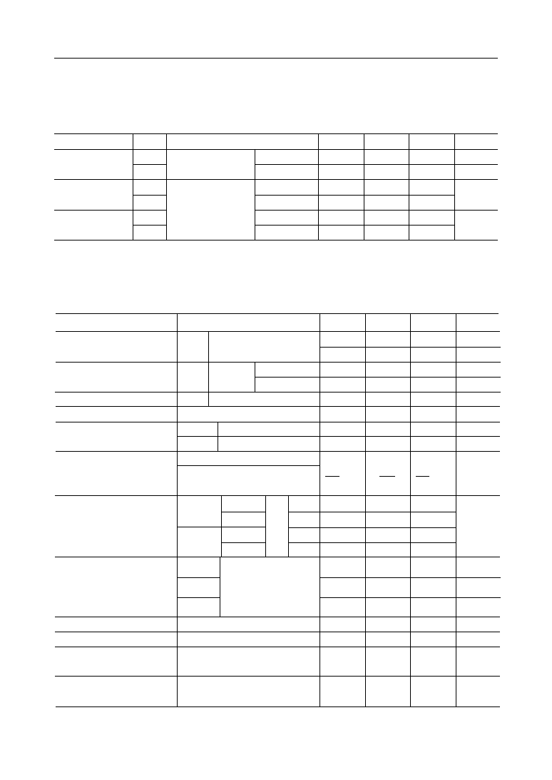
ABSOLUTE MAXIMUM RATINGS
Parameter
Condition
VA, VD
VD2
Rating
≠0.3 to 7
≠0.3 to VD
≠0.3 to VA(VD) + 0.3
≠65 to 150
260
Unit
V
∞C
Symbol
Power Supply Voltage
Input Pin Voltage
Storage Temperature
Pin Soldering Temperature
Ta = 25∞C
with respect to AG and DG
Within 10 sec
--
RECOMMENDED OPERATING CONDITIONS
Power Supply Voltage
Symbol
VA, VD
VD2
4.5
2.5
5.0
--
5.5
VD
V
--
Digital Input Voltage
V
IH
V
IL
2.0
0
--
--
VD
0.8
V
--
Digital Output Current
I
OH
I
OL
≠0.05
--
--
--
--
0.4
mA
When VD2 = VD
(excluding) X2
T
op
≠40
--
+85
--
∞C
Operating Temperature
f
CLK
≠0.1
--
+0.1
--
%
Input Clock Frequency
Bypass Capacitance
VA
VD, VD2
0.1 + 10
1
--
--
--
--
mF
--
Frequency Deviation
At 25∞C ±5∞C
≠100
--
+100
ppm
At ≠40∞C to ±85∞C
≠50
--
+50
Temperature
Characteristics
--
--
--
50
Equivalent Series
Resistance
W
Load Capacitance
--
--
16
--
pF
Crystal
Condition
Min.
Typ.
Max.
Unit
Parameter
9/21
MSM6889
° Semiconductor
ELECTRICAL CHARACTERISTICS
DC and Digital Interface Characteristics
(VA, VD, VD2 = +5 V ±10%, Ta = ≠40∞C to +85∞C)
Digital Output
Voltage
V
OH
I
O =
I
OH
Min.
2.4
--
VD2
V
Digital Input
Current*
I
IH
V
I =
V
IH
Max.
≠10
--
10
µ
A
Power Supply
Current
I
AD
PON = "0"
--
9
12
mA
I
PD
PON = "1"
--
0.01
0.1
mA
I
IL
V
I =
V
IL
Min.
≠100
--
10
V
OL
I
O =
I
OL
Max.
0
--
0.4
I
A
+ I
D
+ I
D2
(VD2 = VD)
Parameter
Symbol
Min.
Typ.
Max.
Unit
Condition
* Internal pull-up resistor
VD2 = VD
Analog Interface and Dynamic Characteristics
Parameter
Condition
Min.
Typ.
Max.
Unit
VA
2
VA + 0.1
2
(VD = VA = 5 V ±10%, Ta = ≠40∞C to +85∞C)
dBm
V
P-P
+1
2.46
≠1
1.95
≠3
1.55
PBG1 to PBG4 Input Data Hold
Time
PBG1 to PBG4 Input Data Setup
Time
PB Tone Distortion
PB Tone Frequency
Out-of-band Energy
Modem Transmit Carrier
Frequency
Output DC Voltage
Signal Level Relative Value
Output Load Resistance
Output Voltage Swing
PB Tone Send Level
Modem Transmit Level
MOD
PB
AO
MOD, PB, GAT2, AO
MODEM
PB Tone
MOD, PB
AO (When GAT1 and GAT2 are
connected)
With respect to nominal frequency
Harmonics/Fundamental
TPBGS, Fig. 7
TPBGH, Fig. 7
R
L
20 kW
"Mark" and "Space" Signals
R
L
20 kW
R
L
20 kW
Low-Group Tone
High-Group Tone
"Mark" & "Space" Signals
High-Gr. Tone & Low-Gr. Tone
P : In-band Signal Energy
(0.3 kHz to 3.4 kHz)
Measured at primary side
of transformer line.
4 to 8 kHz
8 to 12 kHz
12 kHz to
≠8.5
≠7.5
2.2
20
≠2
0
≠ 0.1
976
1176
--
--
--
≠1.5
--
250
250
VA
2
≠6.5
≠5.5
3
--
0
1
980
1180
--
--
--
--
--
--
--
≠4.5
≠3.5
--
--
2
2
984
1184
P-20
P-40
P-60
+1.5
≠23
--
--
dBm
dBm
Vp-p
kW
dB
dB
dB
dB
dB
%
dB
ns
ns
V
1646
1846
1650
1654
Hz
1850
1854
Originate
Mode
Answer
Mode
MARK
SPACE
MARK
SPACE
TD
"1"
"0"
"1"
"0"

10/21
MSM6889
° Semiconductor
Analog Interface and Dynamic Characteristics (Continued)
(VD = VA = 5 V ±10%, Ta = ≠40∞C to +85∞C)
Parameter
Condition
Min.
Typ.
Max.
Unit
Modem Receive Signal Level
AIN+, FSK Demodulator Signal
--
--
≠6
dBm
Carrier Detect (CD) Signal
Level
VR2; Open
--
--
≠42
dBm
OFF∆ON
ON∆OFF
Answer mode: 1080 Hz
Originate mode: 1750 Hz
≠48
--
--
dBm
Answer mode: 1080 Hz
Originate mode: 1750 Hz
1
--
--
dB
CD Level Hysteresis
≠60 dBm ∆ ≠20 dBm Step
10
--
40
ms
CD Delay Time
≠20 dBm ∆ ≠60 dBm Step
0
--
40
ms
CD Hold Time
300 bps, 1/0 Alternative Pattern
--
--
±10
%
Demod. Data Bias Distortion
vNRTS/v Receive Modem Signal
NRTS: 2765 Hz ±30 Hz
--
--
≠2
dB
NRTS Signal-to-Modem
Receive Signal Ratio
400 Hz
≠40
--
≠6
dBm
CPT Detect Level
400 Hz
--
--
≠60
dBm
CPT Non-detect Level
R > 20% (square waves output)
(See Fig. 9)
380
--
420
Hz
CPT Detect Frequency
R > 20% (square waves output)
(See Fig. 9)
CPT Non-detect Frequency
500
--
--
Hz
--
--
300
--
--
20
--
ms
CPT Detect Delay Time
--
--
20
--
ms
CPT Detect Hold Time
For Each Signal Tone
≠46
--
≠6
dBm
PB Tone Detect Amplitude
For Each Signal Tone
--
--
≠60
dBm
PB Tone Non-detect Amplitude
With respect to Nominal Frequency
--
--
±1.5
%
Detect Frequency
With respect to Nominal Frequency
±3.8
--
--
%
Non-detect Frequency
High-Gr. Tone/Low-Gr. Tone
≠6
--
+6
dB
Allowable twist
Noise (0.3 kHz to 3.4 kHz)
Level/Tone Level
--
≠12
--
dB
Allowable Noise Level
380 Hz to 420 Hz
37
--
--
dB
Dial Tone Rejection Ratio
T
C
120
--
--
ms
Signal Repetition Time
T
s
49
--
--
ms
Time to Receive
T
I
--
--
24
ms
Invalid Tone Duration
T
G
24
39
49
ms
Output Delay Time
T
P
30
--
--
ms
Interdigit Pause
T
B
--
--
2
ms
Acceptable Drop Out
T
SP
6
8
10
ms
SP Delay Time
T
D
21
28
35
ms
Output Trailing edge Delay
Fig. 1
Input Impedance
AIN+, 0 to 10 kHz
20
--
--
kW

11/21
MSM6889
° Semiconductor
AIN Signal
PB1 to PB4
SP
T
C
T
S
T
P
T
B
T
G
T
D
T
SP
Figure 1
12/21
MSM6889
° Semiconductor
Figure 2
C1
is an ignorable impedance in the voice frequency band; therefore, if a line transformer and
phone line impedance are ideal (R
L
= 600 W pure resistance), the signal levels at each point are
as shown below.
VT, VR
: Transmit at 2W on phone line, receive signal level (balanced)
VT1, VR1
: Transmit at pin 3 (AIN+), receive signal level (unbalanced)
VAO
: Transmit signal level at pin 5 (AO) (unbalanced)
VT2
: Leaking of transmit signal into receive circuit (unbalanced)
VR2
: Receive signal level of the device (unbalanced)
1) VT = VT1 = 1/2 • VAO
The transmit signal level (voltage) on phone line is half the level at the output pin (AO) of the
device. (600 W : a 600 W line transformer is used)
2) VR1 = VR
3)
Then, where R2 = R3 (e.g., 51 kW), VT2 = 0.
This means that the transmit signal is no longer leaking into the receive circuit.
4)
R
L
VT VR
600 W : 600 W
C1
2.2 mF
R1
600 W
R2
R3
VT1,VR1
VAO
+
≠
+
≠
R2,R3 20 kW
AO
AIN+
AIN≠
GAR
VT2,VR2
3
4
2
5
FUNCTIONAL DESCRIPTION AND APPLICATION
Resistance Hybrid Condition (Ideal Condition)
VT2 = VT1 • (1+ ) + VAO • (≠ )
R3
R2
R3
R2
= VAO • (1+ ) ≠ VAO • = VAO • (1≠ )
R3
R2
R3
R2
1
2
R3
R2
1
2
VR2 = VR1 • (1+ ) , where R2 = R3, VR2 = 2 • VR1 = 2 • VR
R3
R2

13/21
MSM6889
° Semiconductor
Figure 3
The modulation analog signal and PB tone from the modem are not sent at a time. The signal to
be sent is determined by the operating mode specified.
This device is provided with the pins for specifying levels of these transmit signals independently.
The answer tones, which are generated from MODULATOR, are handled as modem signals.
VM : Modem signal level (voltage) at MOD (pin 9)
VP
: PB tone level (voltage) at PB (pin 10)
When the external resistors are R4, R5 and R6, the signal levels at AO (pin 5) are as shown below.
Note : R4, R5, R6
20 kW
As described in "Resistance Hybrid Condition", signal levels actually sent over a phone line will
be half the above mentioned values under the ideal condition.
Setup of Transmit Signal Levels
5
8
7
10
9
VAO
R4
R5
R6
VP
VM
AO
GAT2
GAT1
PB
MOD
PB Tone
Generator
Modulator
R4,R5,R6 20 kW
LPF
+
_
VAO (modem) =
R4
•
VM
R5
VAO (PB) =
R4
•
VP
R6

14/21
MSM6889
° Semiconductor
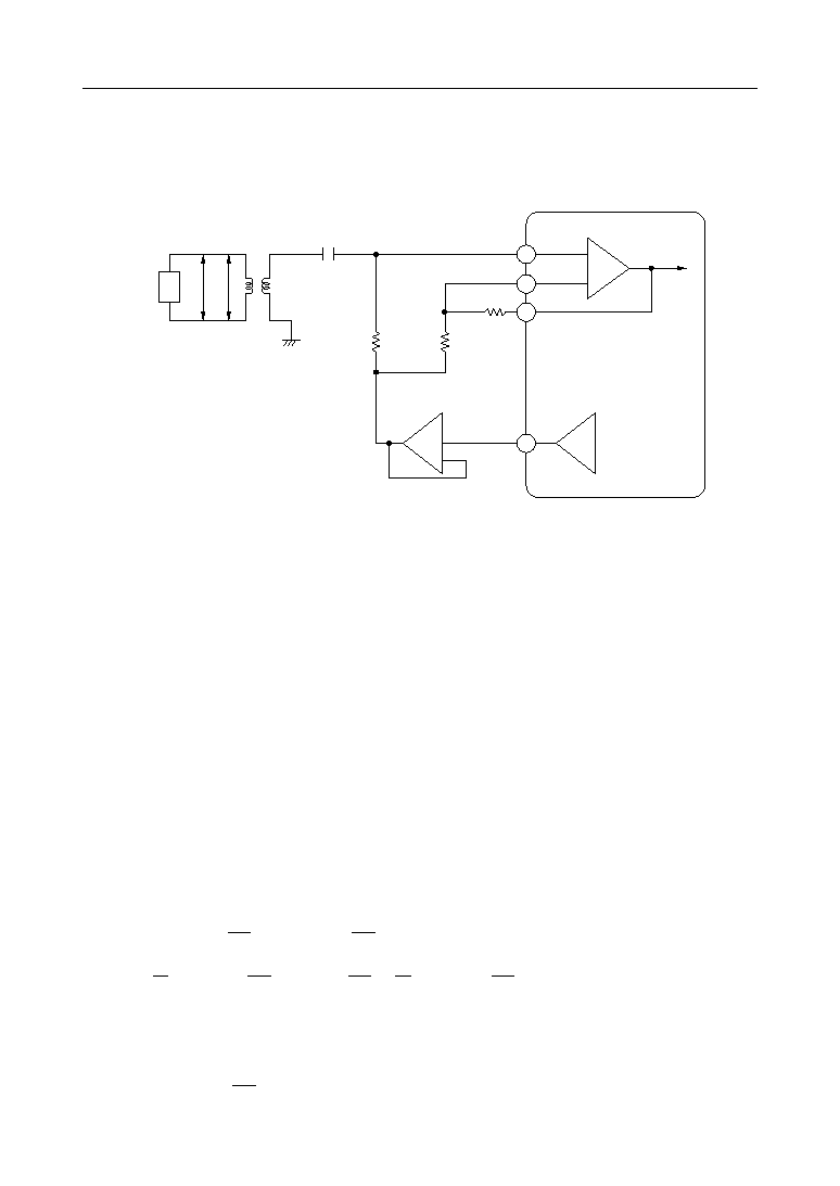
External Setup of Carrier Detect Level
R1
R2
r1
r2
VR1
VR2
SG
VREF
COMP
R1//r1 + R2//r2 20 kW
r1: 250 kW, r2 : 1 MW
11
12
6
*
Mode Select
Functional Block
Operating Mode
CPT REC.
PB GEN.
PB REC.
FSK
MODEM ICT1 = "1" ICT1 = "0"
1
2
3
0
1
O
1
0
1
0
0
1
1
0
0
0
0
0
0
1
1
PB Tone Transmit
PB Tone Detect
Originate Mode
Modem (O)
Answer Mode
Modem (A)
Analog Loop Back
Test (ALB)
Remote Digtal Loop
Back Test (RDLB)
*
*
*
*
*
0
1
1
1
1
1
A
O
A
*
*
*
*
*
*
*
*
0
*
* : Active
When power is turned on or the power down mode is released, put the device into the PB tone
transmit mode or PB tone detect mode.
Figure 4
Operating Mode
Table 1 Operating Mode Table

15/21
MSM6889
° Semiconductor
Line
AIN
AO
Transmit
Filter
Demodulator
Modulator
RD
TD
Receive Data
Transmit
Data
Receive
Filter
Signal flow concept for the modem normal operating mode is shown in Fig. 5.
Figure 5
In the test modes, signal flow shown in Fig. 6 is used. O/(originate)/A(answer) in the test mode
is the expression where the modulator side is referred to as the basis.
[ALB]
AIN
AO
Receive
Filter
Demodulator
RD
TD
Receive Data
Transmit
Data
[RDLB]
AIN
AO
Receive
Filter
Demodulator
Modulator
RD
TD
Receive Data
Transmit
Data
Transmit
Filter
Modulator
Transmit
Filter
Figure 6

16/21
MSM6889
° Semiconductor
PB Tone Transmit Mode and PB Tone Detect Mode
When PBG1 to PBG4 are externally connected to PB1 to PB4 so as to use them as 4-bit bus lines,
their tone generation timings are as shown below.
1)
PB Tone Transmit Mode
When TEN is in the digital "0" state, PB tone is generated according to Table 2.
TEN
PBG1/PB1
PBG2/PB2
PBG3/PB3
PBG4/PB4
PB
TPBGS
TPBGH
941 Hz + 1477 Hz
Figure 7
2)
PB Tone Detect Mode
AIN
PB1/PBG1
PB2/PBG2
PB3/PBG3
PB4/PBG4
TG
TD
"0"
"1"
"0"
"1"
"1"
"1"
"1"
TSP
"0"
SP
941 Hz + 1477 Hz
852 Hz + 1209 Hz
Figure 8

17/21
MSM6889
° Semiconductor
Table 2 PB Tone Code Table
Button
Low-Group Freq. (Hz)
High-Group Freq. (Hz)
697
770
852
941
1209
1336
1477
1633
PB4/
PBG4
PB3/
PBG3
PB2/
PBG2
PB1/
PBG1
1
2
3
4
5
6
7
8
9
0
*
#
A
B
C
D
*
*
*
*
*
*
*
*
*
*
*
*
*
*
*
*
*
*
*
*
*
*
*
*
*
*
*
*
*
*
*
*
0
0
0
0
0
0
0
1
1
1
1
1
1
1
1
0
0
0
0
1
1
1
1
0
0
0
0
1
1
1
1
0
0
1
1
0
0
1
1
0
0
1
1
0
0
1
1
0
1
0
1
0
1
0
1
0
1
0
1
0
1
0
1
0
Call Progress Tone (CPT) Detect Mode
AIN
CP
ICT1 = "1"
CP
ICT1 = "0"
400 Hz
TW TD
R = TW/(TD + TW) • 100 [%]
Figure 9

18/21
MSM6889
° Semiconductor
APPLICATION CIRCUIT
Pin Connection
1
VA
2
GAR
3
AIN+
4
AIN≠
5
AO
6
SG
7
GAT1
8
GAT2
9
MOD
10
PB
11
VR1
12
VR2
13
AG
14
PBG1
15
PBG2
16
PBG3
17
PBG4
18
TEN
19
TD
20
RS
21
DG
42
41
40
39
38
37
36
35
34
33
32
31
30
29
28
27
26
25
24
23
22
VD
VD2
NC
PON
SP
PB4
PB3
PB2
PB1
CP
CD
RD
CLK
X2
X1
MODE3
MODE2
MODE1
ICT3
ICT2
ICT1
MSM6889RS
≠
+
≠
+
C2
C3
R3
C1
R1
R2
+
≠
R4
R5
R6
3.579545
MHz
R1 = 600 W, R2 = R3 = R4 = R5 = R6 = 51 kW
C1 = 2 mF, C2 = C3 = 10 mF
19/21
MSM6889
° Semiconductor
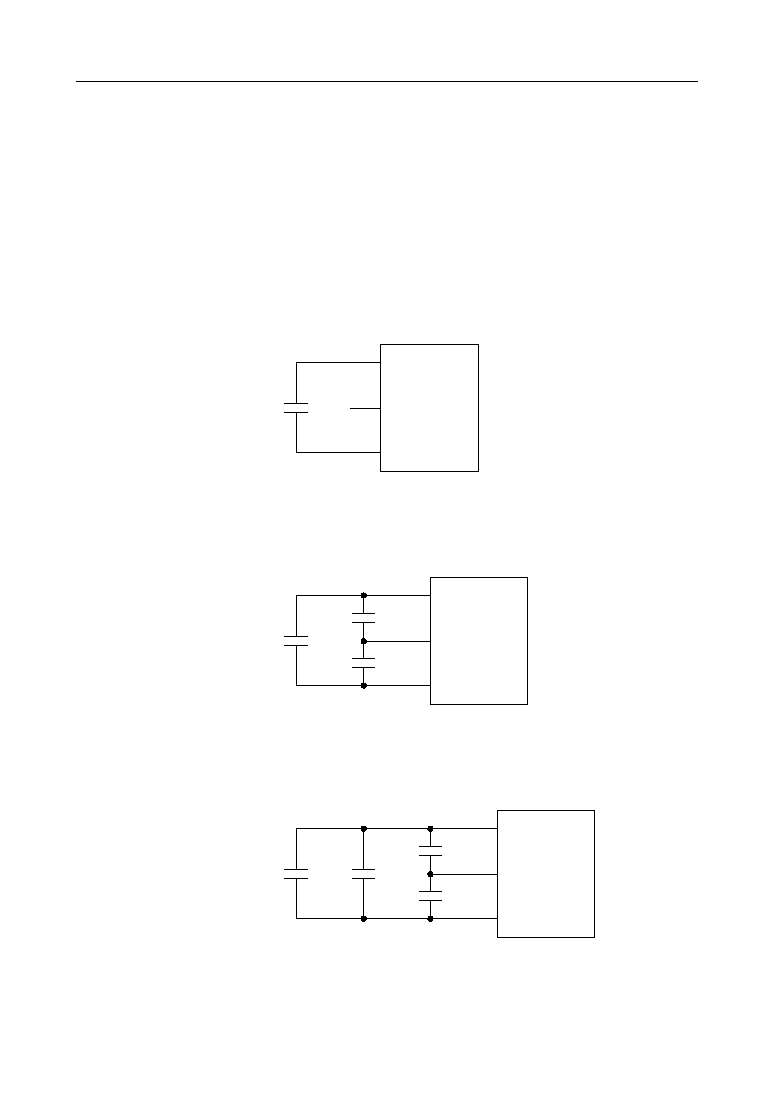
Bypass Capacitor Connections
The MSM6889 contains analog circuits.
Note that noise occurred in the power supply by trouble in other circuits may cause degradation
in characteristics of the device.
The examples of connected bypass capacitors of the MSM6889 are shown below.
VA, VD
SG
AG, DG
MSM6889
10 mF to 47 mF
VA, VD
SG
AG, DG
MSM6889
10 mF to 47 mF
1 mF
1 mF
VA, VD
SG
AG, DG
MSM6889
10 mF to 47 mF
*1 mF
10 mF
10 mF
* Laminated ceramic capacitor

20/21
MSM6889
° Semiconductor
(Unit : mm)
PACKAGE DIMENSIONS
DIP42-P-600-2.54
Package material
Lead frame material
Pin treatment
Solder plate thickness
Package weight (g)
Epoxy resin
42 alloy
Solder plating
5 mm or more
6.20 TYP.

21/21
MSM6889
° Semiconductor
(Unit : mm)
Notes for Mounting the Surface Mount Type Package
The SOP, QFP, TSOP, SOJ, QFJ (PLCC), SHP and BGA are surface mount type packages, which
are very susceptible to heat in reflow mounting and humidity absorbed in storage.
Therefore, before you perform reflow mounting, contact Oki's responsible sales person for the
product name, package name, pin number, package code and desired mounting conditions
(reflow method, temperature and times).
QFP56-P-1519-1.00-K
Package material
Lead frame material
Pin treatment
Solder plate thickness
Package weight (g)
Epoxy resin
42 alloy
Solder plating
5 mm or more
1.46 TYP.
Mirror finish