 | –≠–ª–µ–∫—Ç—Ä–æ–Ω–Ω—ã–π –∫–æ–º–ø–æ–Ω–µ–Ω—Ç: MSM6926 | –°–∫–∞—á–∞—Ç—å:  PDF PDF  ZIP ZIP |

° Semiconductor
MSM6926/6946
1/25
° Semiconductor
MSM6926/6946
300 bps Single Chip FSK MODEM
GENERAL DESCRIPTION
The MSM6926 and the MSM6946 are OKI's 300 bps single chip modem series which transmit and
receive serial, binary data over a switched telephone network using frequency shift keying (FSK).
The MSM6926 is compatible with ITU-T V.21 series data sets, while the MSM6946 is compatible
with Bell 103 series data sets.
These devices provide all the necessary modulation, demodulation, and filtering required to
implement a serial, asynchronous communication link.
OKI's single chip modem series is designed for users who are not telecommunication experts and
are easy to use cost effective alternative to standard discrete modem design.
CMOS LSI technology provides the advantages of small size, low power, and increased
reliability.
The design of the integrated circuit assures compatibility with a broad base of installed low speed
modems and acoustic couplers. Applications include interactive terminals, desk top computers,
point of sale equipment, and credit verification systems.
FEATURES
∑ Compatible with ITU-T V.21 (MSM6926)
∑ Compatible with BELL 103 (MSM6946)
∑ CMOS silicon gate process
∑ Switched capacitor and advanced CMOS analog technology
∑ Data rate from 0 to 300 bps
∑ Full duplex (2-Wire)
∑ Originate and Answer modes
∑ Selectable built-in timers and external delay timers possible
∑ All filtering, modulation, demodulation, and DTE interface on chip
∑ TTL compatible digital interface
∑ Low power dissipation: 90 mW Typ.
∑ Package options:
28-pin plastic DIP
(DIP28-P-600-2.54)
(Product name: MSM6926RS)
(Product name: MSM6946RS)
44-pin plastic QFP
(QFP44-P-910-0.80-K)
(Product name: MSM6926GS-K)
(Product name: MSM6946GS-K)
(QFP44-P-910-0.80-2K)
(Product name: MSM6926GS-2K)
(Product name: MSM6946GS-2K)
E2A0009-16-X1
This version: Jan. 1998
Previous version: Nov. 1996
° Semiconductor
MSM6926/6946
2/25
BLOCK DIAGRAM
SG1
V
A
V
D
DG
AIN
M
FT
AO
V
A
AG
SG1
SG2
V
REF
X1
X2
CLK
TS1
TS2
AG
SG2
CDR2
CDR1
RD1
RD2
CD2
RD
RS1
RS2
CS
CC
LT
CD1
XD
Carrier Detect
Demodulator
Receive Filter
Modulator
Transmit Filter
Clock Gen.
OSC
SW
ROM
Cont.
DTE
Inter-
face
Loop
Test
Delay
° Semiconductor
MSM6926/6946
3/25
PIN CONFIGURATION (TOP VIEW)
TS2
28
TS1
27
V
D
26
AO
25
V
A
24
FT
23
M
22
AIN
21
SG1
20
AG
19
SG2
18
CDR2
17
CDR1
16
DG
15
X1 1
X2 2
CLK 3
LT 4
CC 5
CS 6
RS1 7
RS2 8
XD 9
RD 10
CD1 11
CD2 12
RD1 13
RD2 14
44-Pin Plastic QFP
11
10
9
8
7
6
5
4
3
2
1
23
24
25
26
27
28
29
30
31
32
33
AG
SG1
NC
AIN
NC
NC
NC
NC
M
FT
V
A
NC
RD
XD
RS2
NC
NC
NC
RS1
CS
CC
NC
28-Pin Plastic DIP
44
43
42
34
35
36
37
38
39
40
41
NC
V
D
AO
TS1
LT
X2
X1
NC
V
A
*
TS2
CLK
12
13
14
22
21
20
19
18
17
16
15
DG
CDR2
SG2
CDR1
CD1
CD2
RD1
NC
RD2
V
A
*
NC
Note:
*: Both No. 17 pin and No. 39 pin are set to be at V
A
level by setting No. 33 pin at V
A
level.
NC: No connect pin
° Semiconductor
MSM6926/6946
4/25
PIN DESCRIPTIONS
Power
DG
15
19
--
Ground reference of V
D
(digital ground)
AG
19
23
--
Ground reference of V
A
(digital ground)
V
A
24
33
--
Supply voltage (+12 V nominal)
V
D
26
35
--
Supply voltage (+5 V nominal)
Name
Pin No.
RS GS-K
I/O
Description
Clocks
X1
1
41
Master clock timing is provided by either a series resonant crystal (3.579545 MHz
±0.01%) connected across X1 and X2, or by an external TTL/CMOS clock driving
X2 with AC coupling. In this latter case, X1 is left unconnected.
See Fig. 10.
X2
2
42
--
CLK
3
43
O
873.9 Hz clock output. This clock is used to implement external delay circuits etc.
Name
Pin No.
RS GS-K
I/O
Description
--
° Semiconductor
MSM6926/6946
5/25
Control
LT
4
44
I
Digital loop back test. During digital "High", any data sent on the X
D
pin will appear
on the RD pin, and any data sent on the RS1 pin will immediately appear on the
CS pin. Any data demodulated from the received carrier on the A
IN
pin will be the
modulated data to implement the transmitted carrier. In this case, sending the
transmitted carrier to the phone line depends on the CC, but never on RS1.
During digital loop back test, the data on this pin becomes a control signal for sending
the transmitted carrier to the phone line in place of RS1.
CC
5
2
I
When an external circuit gives the RS/CS delay time which is not within the device
as required, this pin should be connected to the external circuit output.
See Fig. 11.
RS2
8
8
I
The fast carrier detection output. This pin is internally connected to the input of
the built-in carrier detect delay circuit. When an external delay circuit provides
the delay time which is not within the device as required, the CD1 should be
connected to the external circuit input. See Fig. 11.
CD1
11
12
O
Name
Pin No.
RS GS-K
I/O
Description
CD2
12
13
I/O
When an external circuit gives the carrier detect delay time which is not within
the device as required, this pin becomes the input pin for the external circuit
output signal. In other cases (when using the delay time within the device, the
data on the TS1 or TS2 is not digital "High"), this pin becomes the Carrier detect
signal output.
The RD1 data is demodulated data from the received carrier and the RD2 is the
input of the following logic circuits referred to in Fig. 12. Usually, the RD1 data
is input directly to RD2. In some cases, as input data to RD2, the data that is
controlled by NCU (Network control unit) etc. may be required in stead of the
RD1 data.
RD1
13
14
O
RD2
14
16
I
These two pins are the output (CRD1) and inverting input (CDR2) of the buffer
operational amplifier of which the noninverting input is connected to the built-in
voltage reference, stabilized to variations in the supply voltage and temperature.
See Fig. 13. An adequate carrier-detect level can be set by selecting the ratio of
R
8
to R
9
. Therefore, the loss in the received carrier level by phone-line
transformer can be compensated by adjusting the ratio of R
8
to R
9
. R
8
+ R
9
should be greater than 50 k
W.
CDR1
16
20
O
CDR2
17
21
I
Answer/Originate mode select. During digital "High", the originate mode is
selected. A low input selects the answer mode.
M
22
31
I
This pin may be used for device tests only. During digital "High", the A
O
pin will
be connected to receiving filter output instead of transmitting filter output.
FT
23
32
I
RS/CS delay and carrier detect delay options referred to chapter about timing
characteristics are selected by TS1 and TS2 inputs. Be careful that each delay
can not be individually selected. If another delay time than the ones within the
device are required as an option, input a digital "High" to the TS1 and TS2 pin
and implement the external delay circuits to obtain the desired delay
characteristics. In this case, the CD2 pin becomes not only the input for the
external circuit output signal, but also the Carrier detect output. See Fig. 11.
TS1
27
36
I
TS2
28
38
I
° Semiconductor
MSM6926/6946
6/25
Input/Output
Name
Pin No.
RS GS-K
I/O
Description
CS
6
3
O
Clear to send signal output. The digital "High" level indicates the "OFF" state and
digital "Low" indicates the "ON" state. This output goes "Low" at the end of a delay
(RS/CS delay) initiated when RS1 (Request to send) goes "Low".
Request to send signal input. The digital "High" level indicates the "OFF" state.
The digital "Low" level indicates the "ON" state and instructs the modem to enter
the transmit mode. This input must remain "Low" for the duration of data
transmission. "High" turns the transmitter off.
RS1
7
4
I
This is digital data to be modulated and transmitted via A
O
. Digital "High" will be
transmitted as "Mark". Digital "Low" will be transmitted as "Space". No signal
appears at A
O
unless RS1 is "Low".
XD
9
9
I
Digital data demodulated from A
IN
is serially available at this output. Digital
"High" indicates "Mark" and digital "Low" indicates "Space". For example, under
the following condition, this output is forced to be "Mark" state because the data
may be invalid.
∑ When CD2 (Carrier detect) is in the "OFF" state.
RD
10
10
O
The SG1 and ST2 are built-in analog signal grounds. SG2 is used only for
Carrier detect function. The DC voltage of SG1 is approximately 6 V, so the
analog line interface must be implemented by AC coupling. See Fig. 9. To make
impedance lower and ensure the device performance, it is necessary to put
bypass capacitors on SG1 and SG2 in close physical proximity to the device.
SG2
18
22
O
SG1
20
24
O
This is the input for the analog signal from the phone line. The modem extracts
the information in this modulated carrier and converts it into a serial data stream
for presentation at RD output.
A
IN
21
26
I
This analog output is the modulated carrier to be conditioned and sent over the
phone line.
A
O
25
34
O
° Semiconductor
MSM6926/6946
7/25
ABSOLUTE MAXIMUM RATINGS
Parameter
Power Supply Voltage
Symbol
V
A
V
D
Condition
Ta = 25∞C
With respect
to AG or DG
Rating
≠0.3 to 15
≠0.3 to 7
Unit
V
Analog Input Voltage
Digital Input Voltage
Operating Temperature
Storage Temperature
V
IA
V
ID
T
op
T
STG
--
--
≠0.3 to V
A
+ 0.3
≠0.3 to V
D
+ 0.3
0 to +70
≠55 to 150
∞C
*1
*2
*1
*2
CDR2, A
IN
X1, LT, CC, RS1, RS2, XD, CD2, RD2, M, FT, T
S1
, T
S2
*3
*3
CD2 is I/O terminal
° Semiconductor
MSM6926/6946
8/25
RECOMMENDED OPERATING CONDITIONS
Parameter
Unit
Max.
Typ.
Min.
Symbol
Condition
Power Supply Voltage
V
13.2
12.0
10.8
VA
With respect to AG
5.25
5.00
4.75
VD
With respect to DG
--
0
--
AG, DG
--
Operating Temperature
70
--
0
T
op
--
∞C
CRYSTAL
--
3.579545
--
--
--
MHz
Transformer
impedance = 600
W
R
1
--
600
--
W
R
2
--
51
--
--
k
W
R
3
--
51
--
R
4
--
51
--
R
5
--
51
--
R
6
--
51
--
R
7
--
51
--
R
8
--
33
--
R
9
--
51
--
C
0
, C
1
--
0.047
--
C
2
--
2.2
--
C
3
--
--
22
C
4
--
--
0.01
C
5
--
10
--
C
6
--
10
--
mF
--
Application circuits using above conditions are provided in Fig. 8.
--
--
--
--
--
--
--
--
--
--
--
--
--
--
--
° Semiconductor
MSM6926/6946
9/25
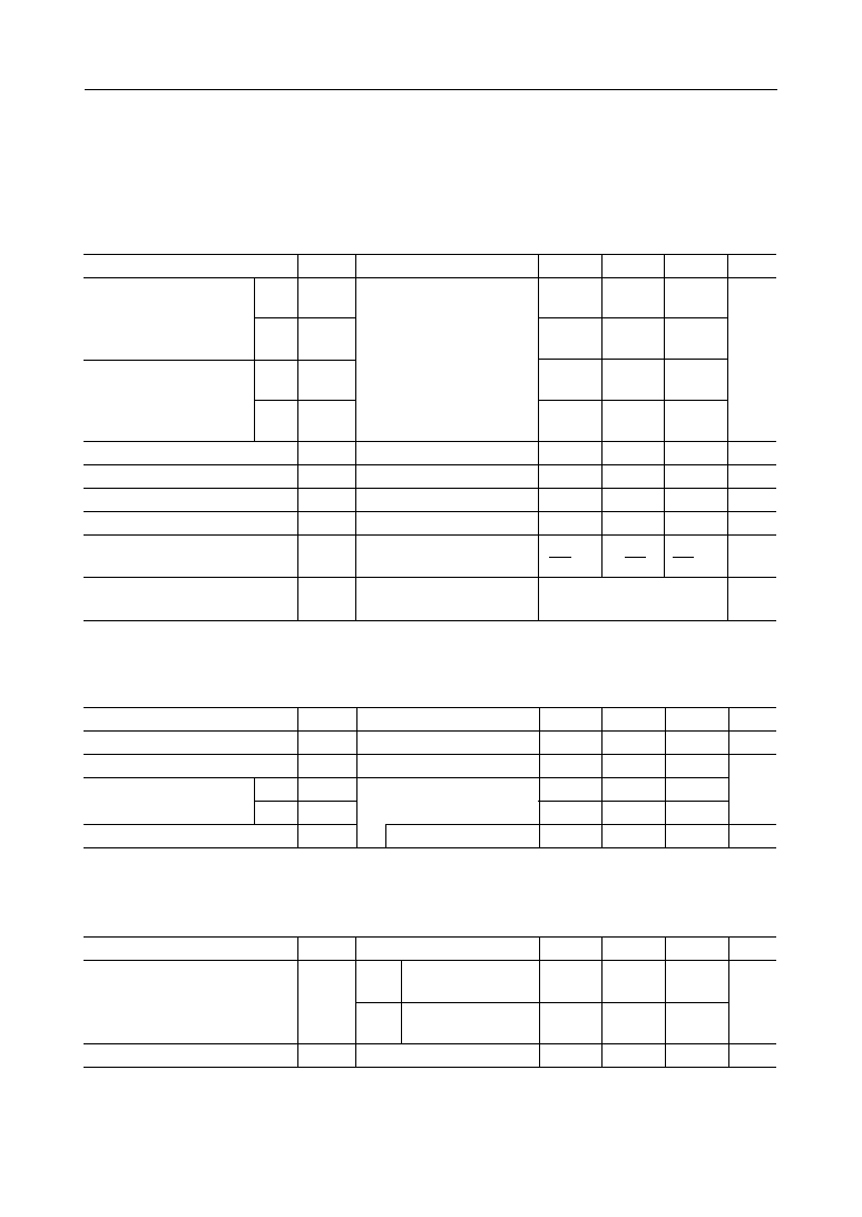
ELECTRICAL CHARACTERISTICS
DC and Digital Interface Characteristics
Parameter
Unit
Max.
Typ.
Min.
Symbol
Condition
Power Supply Current
mA
15.0
7.5
--
I
A
Ordinary
operation
2.0
1.0
--
I
D
10
--
≠10
I
IL
V
I
= 0 V
Input Leakage Currnet
10
--
≠10
I
IH
V
I
= V
D
mA
Input Voltage
0.8
--
0
V
IL
--
V
(V
A
= 12 V ±10%, V
D
= 5 V ±5%, Ta = 0 to 70∞C)
*1
V
D
--
2.2
V
IH
--
*1
Output Voltage
0.4
--
0
V
OL
I
OL
= 1.6 mA
V
D
--
0.8
• VD
V
OH
I
OH
= 400
mA
*2
*1 LT, CC, RS1, RS2, XD, CD2, RD2, M, FT, T
S1
, T
S2
*2 CLK, CS, RD, CD1, CD2, RD1
*3
*3
*3 CD2 is I/O terminal.
° Semiconductor
MSM6926/6946
10/25
Analog Interface Characteristics
1. MSM6926
Transmit carrier out (A
O
)
Receive carrier input (A
IN
)
Receive filter
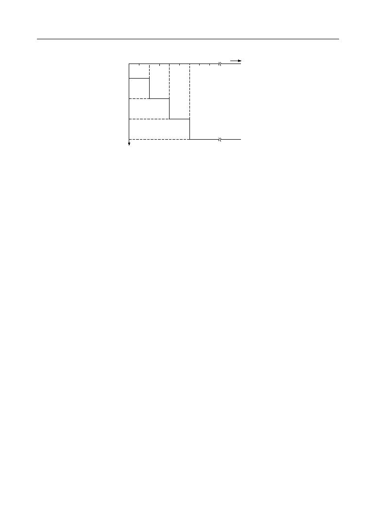
Notes: *1 0 dBm = 0.775 Vrms
*2 The resistor values are typical
--
Parameter
Unit
Max.
Typ.
Min.
Symbol
Condition
ORIGINATE MODE
Carrier Frequency
Hz
986
980
974
f
OM
f
CRYSTAL
= 3.579545 MHz
(V
A
= 12 V ±10%, V
D
= 5 V ±5%, Ta = 0 to 70∞C)
Mark
1
1186
1180
1174
f
OS
Space
0
ANSWER MODE
Carrier Frequency
1656
1650
1644
f
AM
Mark
1
1856
1850
1844
f
AS
Space
0
Output Resistance
200
--
--
R
OXA
W
--
Load Resistance
--
--
50
R
LXA
k
W
--
Load Capacitance
100
--
--
C
LXA
pF
--
Transmit Level
8
6
4
V
OXA
*1 dBm
--
Output Offset Voltage
V
A
2
V
OSX
V
≠1
V
A
2
V
A
2
+ 1
C
1
= 0.047
mF
Out-of-Band Energy
(Referred to Carrier Level)
Refer to Fig. 1
E
OX
dB
Parameter
Unit
Max.
Typ.
Min.
Symbol
Condition
Input Resistance
k
W
--
--
100
R
IRA
--
Receive Signal Level Range
*1 dBm
≠6
--
≠48
V
IRA
--
Carrier Detect Level
≠43
--
--
V
CD
ON
R
8
= 33 k
W
R
9
= 51 k
W
--
--
≠48
V
CD
OFF
ON
OFF
*2
Carrier Detect Hysteresis
dB
--
--
2
H
YS
V
CD
ON ≠ V
CD
OFF
Parameter
Unit
Max.
Typ.
Min.
Symbol
Condition
Group Delay Distortion
ms
--
800
--
D
DL
ORIG.
MODE
--
850
--
ANS.
MODE
1600 to 1900 Hz
V
AIN
= ≠6 dBm
Adjacent Channel Rejection
L
AC
--
--
50
dB
930 to 1230 Hz
° Semiconductor
MSM6926/6946
11/25
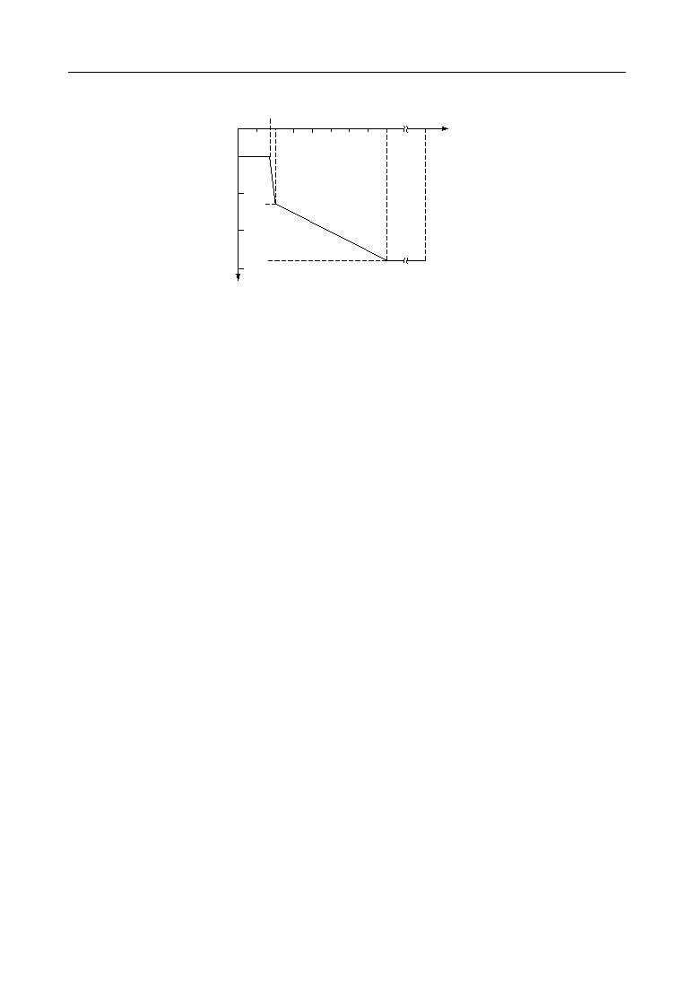
Figure 1 MSM6926 Out-of-Band Energy Referred to Carrier Level (C
1
= 0.047
mF)
kHz
0
≠20
≠40
≠60
0
2
4
6
8 10 12 14 16
dB
° Semiconductor
MSM6926/6946
12/25
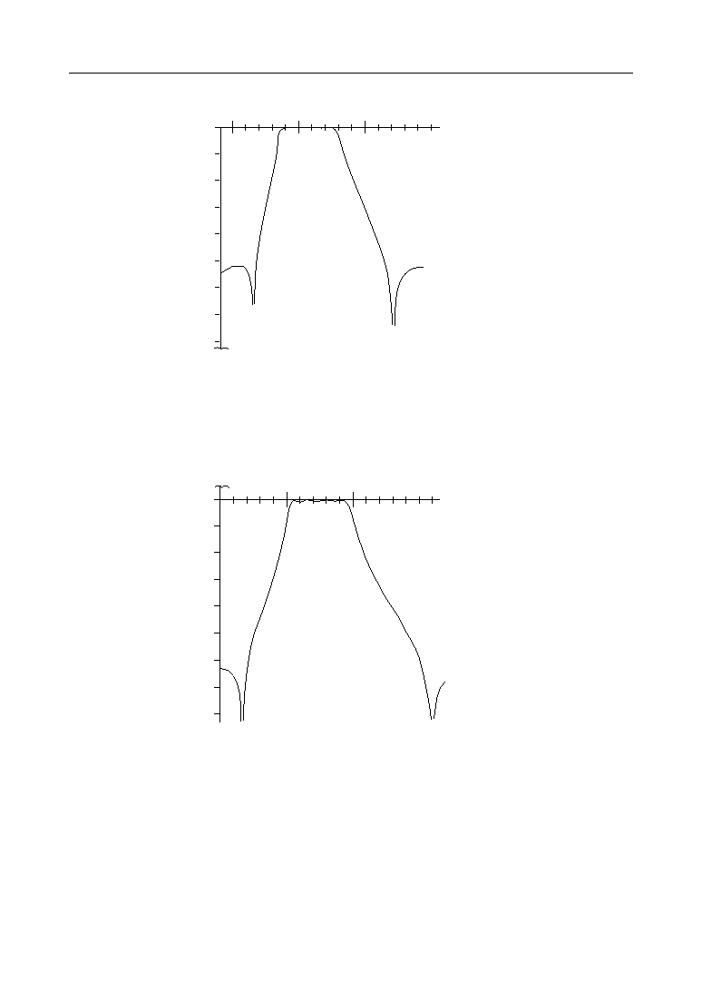
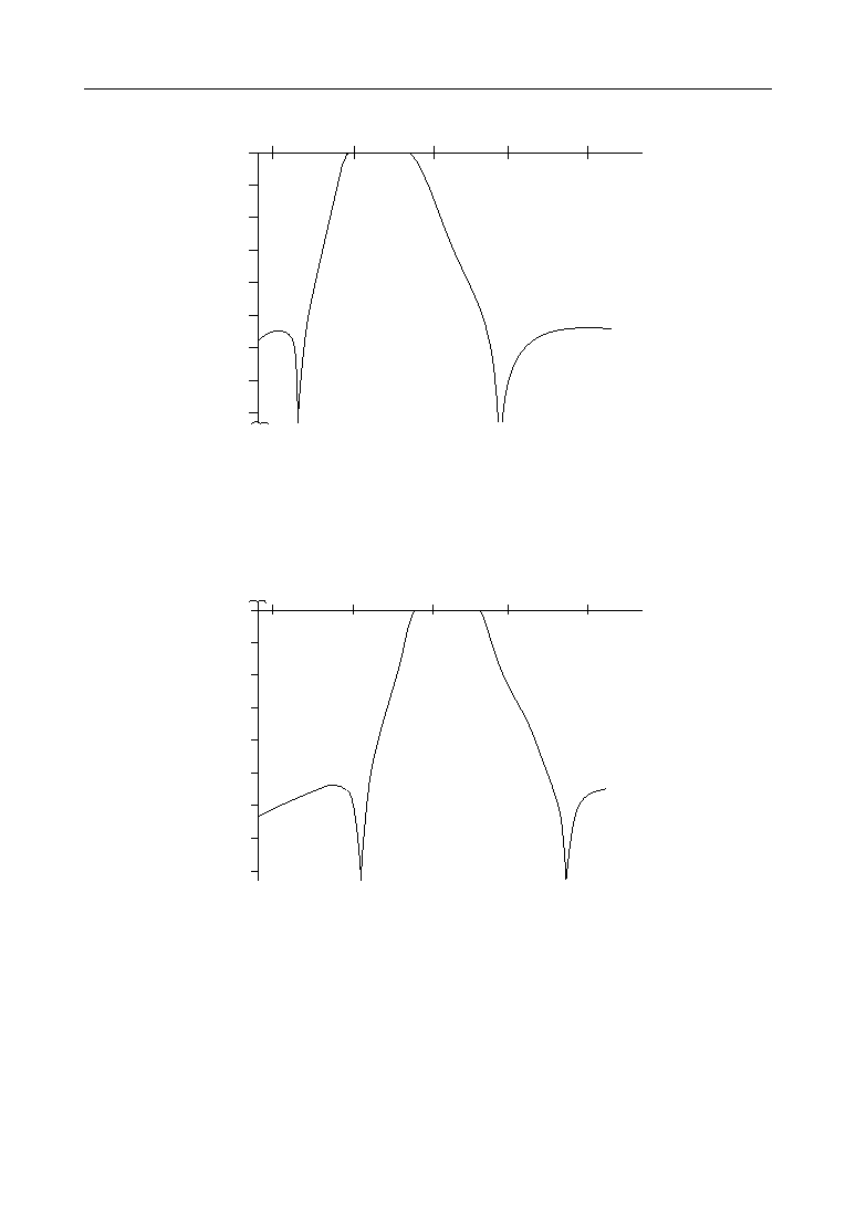
Figure 2 MSM6926 Low Band Filter
Figure 3 MSM6926 High Band Filter
0
≠10
≠20
≠30
≠40
≠50
≠60
≠70
≠80
500
1000
1500
Frequency (Hz)
Gain (dB)
0
≠10
≠20
≠30
≠40
≠50
≠60
≠70
≠80
1500
2000
Frequency (Hz)
Gain (dB)
° Semiconductor
MSM6926/6946
13/25
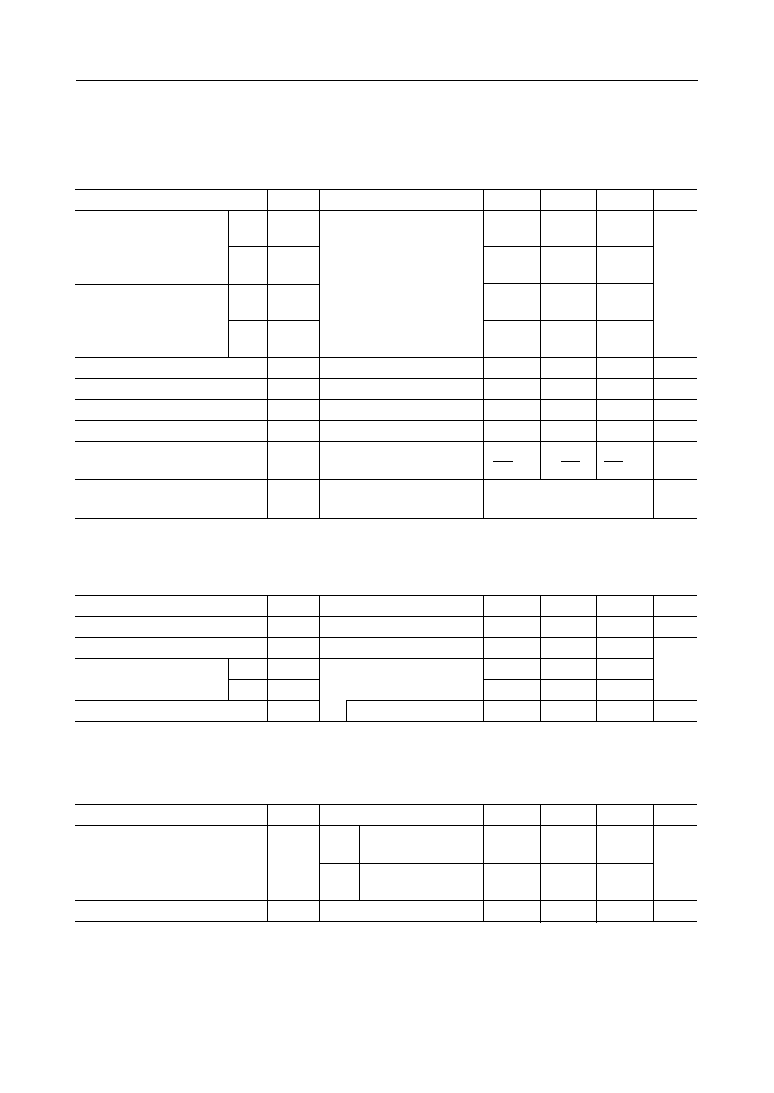
2. MSM6946
Transmit carrier out (A
O
)
Receive carrier input (A
IN
)
Receive Filter
Notes: *1 0 dBm = 0.775 Vrms
*2 The resistor values are typical
--
Parameter
Unit
Max.
Typ.
Min.
Symbol
Condition
ORIGINATE MODE
Carrier Frequency
Hz
1276
1270
1264
f
OM
f
CRYSTAL
= 3.579545 MHz
(V
A
= 12 V ±10%, V
D
= 5 V ±5%, Ta = 0 to 70∞C)
Mark
1
1076
1070
1064
f
OS
Space
0
ANSWER MODE
Carrier Frequency
2231
2225
2219
f
AM
Mark
1
2031
2025
2019
f
AS
Space
0
Output Resistance
200
--
--
R
OXA
W
--
Load Resistance
--
--
50
R
LXA
k
W
--
Load Capacitance
100
--
--
C
LXA
pF
--
Transmit Level
8
6
4
V
OXA
*1 dBm
--
Output Offset Voltage
V
A
2
V
OSX
V
≠1
V
A
2
V
A
2
+ 1
C
1
= 0.047
mF
Out-of-Band Energy
(Referred to Carrier Level)
Refer to Fig. 4
E
OX
dB
Parameter
Unit
Max.
Typ.
Min.
Symbol
Condition
Input Resistance
k
W
--
--
100
R
IRA
--
Receive Signal Level Range
*1 dBm
≠6
--
≠48
V
IRA
--
Carrier Detect Level
≠43
--
--
V
CD
ON
R
8
= 33 k
W
R
9
= 51 k
W
--
--
≠48
V
CD
OFF
ON
OFF
*2
Carrier Detect Hysteresis
dB
--
--
1.5
H
YS
V
CD
ON ≠ V
CD
OFF
Parameter
Unit
Max.
Typ.
Min.
Symbol
Condition
Group Delay Distortion
ms
--
650
--
D
DL
ORIG.
MODE
--
750
--
ANS.
MODE
1975 to 2275 Hz
V
AIN
= ≠6 dBm
Adjacent Channel Rejection
L
AC
--
--
50
dB
1020 to 1320 Hz
° Semiconductor
MSM6926/6946
14/25
Figure 4 MSM6946 Out-of-Band Energy Referred to Carrier Level (C
1
= 0.047
mF)
kHz
0
≠20
≠40
≠60
0
2
4
6
8 10 12 14 16
dB
200
≠25
≠55
3.4
15 dB/OCTAVE
° Semiconductor
MSM6926/6946
15/25
Figure 5 MSM6946 Low Band Filter
Figure 6 MSM6946 High Band Filter
0
≠10
≠20
≠30
≠40
≠50
≠60
≠70
≠80
500
1000
1500
2000
2500
Frequency (Hz)
Gain (dB)
0
≠10
≠20
≠30
≠40
≠50
≠60
≠70
≠80
1000
1500
2000
2500
3000
Frequency (Hz)
Gain (dB)
° Semiconductor
MSM6926/6946
16/25
Demodulated Bit Characteristics
Timing Characteristics
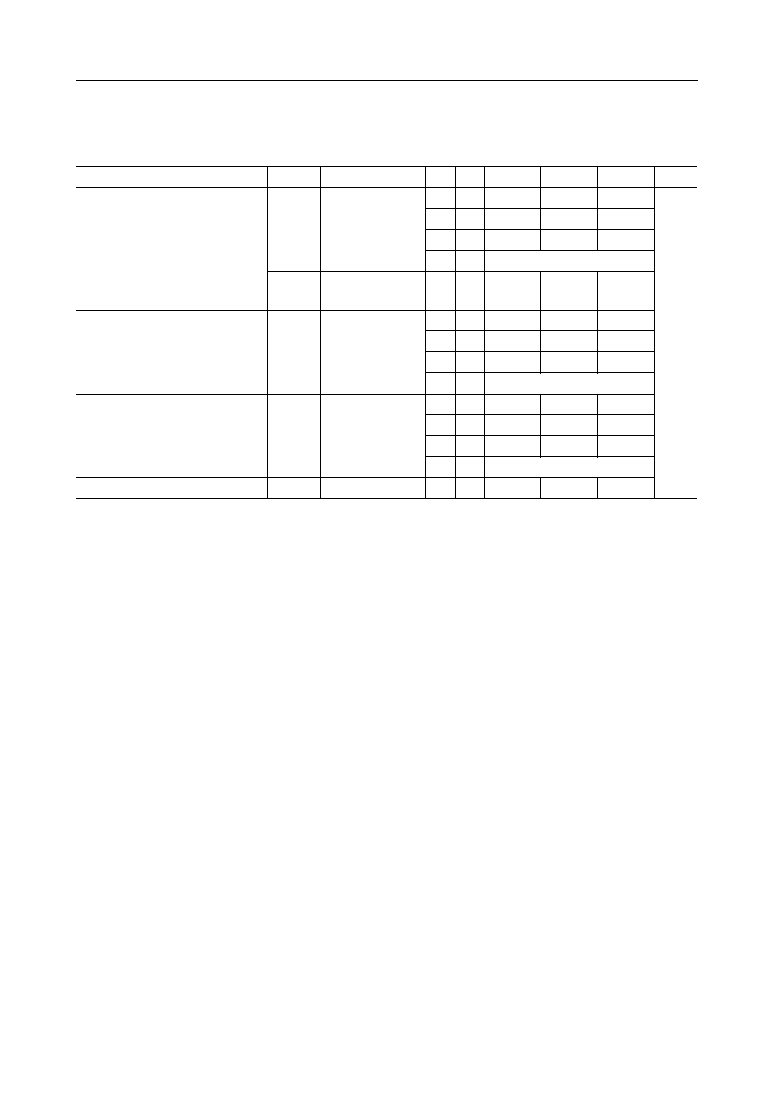
1. MSM6926
Parameter
Unit
Max.
Typ.
Min.
Symbol
Condition
RS/CS Delay Time
ms
405
400
395
T
RC
ON
RS1 = "0"
∆ CS = "0"
(V
A
= 12 V ±10%, V
D
= 5 V ±5%, Ta = 0 to 70∞C)
TS1
TS2
0
0
35
30
25
0
1
355
350
345
1
0
External delay timer
1
1
RS1 = "1"
∆ CS = "1"
T
RC
OFF
0.5
--
0
*
*
320
--
300
0
0
20
--
5
0
1
170
--
150
1
0
External delay timer
1
1
CD/ON Delay Time
T
CD
ON
--
70
--
20
0
0
70
--
20
0
1
40
--
10
1
0
External delay timer
1
1
CD/OFF Delay Time
T
CD
OF
--
Soft Turn-OFF Time
T
ST
*
*
--
10
--
--
Refer to Fig. 7
Notes: *: Irrespective of I/O condition
Parameter
Unit
Max.
Typ.
Min.
Symbol
Condition
Peak Intersymbol Distortion
%
--
6
--
ID
Back-to-back over input
signal range ≠6 to ≠40 dBm.
511-bit test pattern.
(V
A
= 12 V ±10%, V
D
= 5 V ±5%, Ta = 0 to 70∞C)
5 dB
--
S/N
Back-to-back with 0.3 to
3.4 kHz flat noise.
Receive signal level ≠25 dBm.
511-bit test pattern
Bit Error Rate
--
10
≠5
--
BER
° Semiconductor
MSM6926/6946
17/25
2. MSM6946
Parameter
Unit
Max.
Typ.
Min.
Symbol
Condition
RS/CS Delay Time
ms
205
200
195
T
RC
ON
RS1 = "0"
∆ CS = "0"
(V
A
= 12 V ±10%, V
D
= 5 V ±5%, Ta = 0 to 70∞C)
TS1
TS2
0
0
--
+
--
0
1
--
+
--
1
0
External delay timer
1
1
RS1 = "1"
∆ CS = "1"
T
RC
OFF
0.5
--
0
*
*
120
--
100
0
0
--
+
--
0
1
--
+
--
1
0
External delay timer
1
1
CD/ON Delay Time
T
CD
ON
--
50
--
10
0
0
--
+
--
0
1
--
+
--
1
0
External delay timer
1
1
CD/OFF Delay Time
T
CD
OF
--
Soft Turn-OFF Time
T
ST
*
*
--
10
--
--
Refer to Fig. 8
Notes: *: Irrespective of I/O condition
+: Reserved
° Semiconductor
MSM6926/6946
18/25
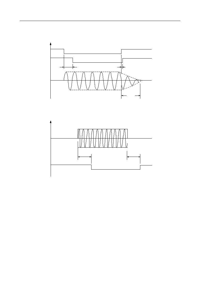
TIMING DIAGRAM
RS1
CS
AO
T
RCON
T
RCOFF
T
ST
T
CDON
T
CDOFF
CD2
AIN
Figure 7 MSM6926/6946 Timing Diagram
° Semiconductor
MSM6926/6946
19/25
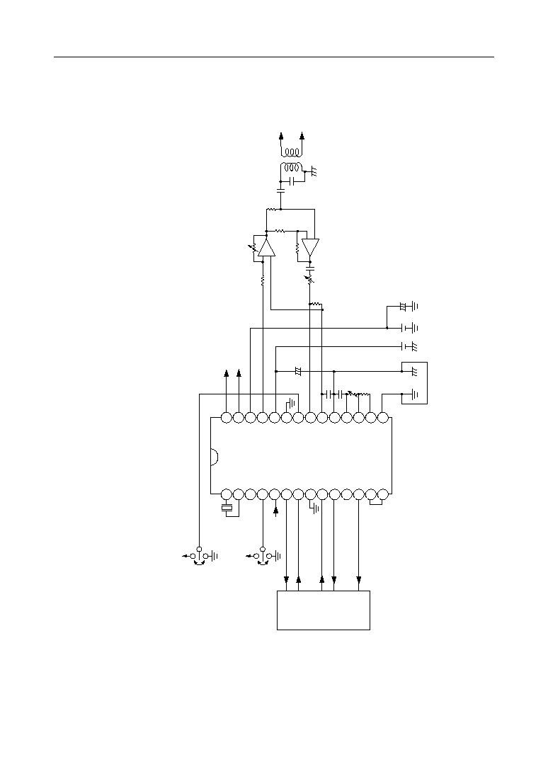
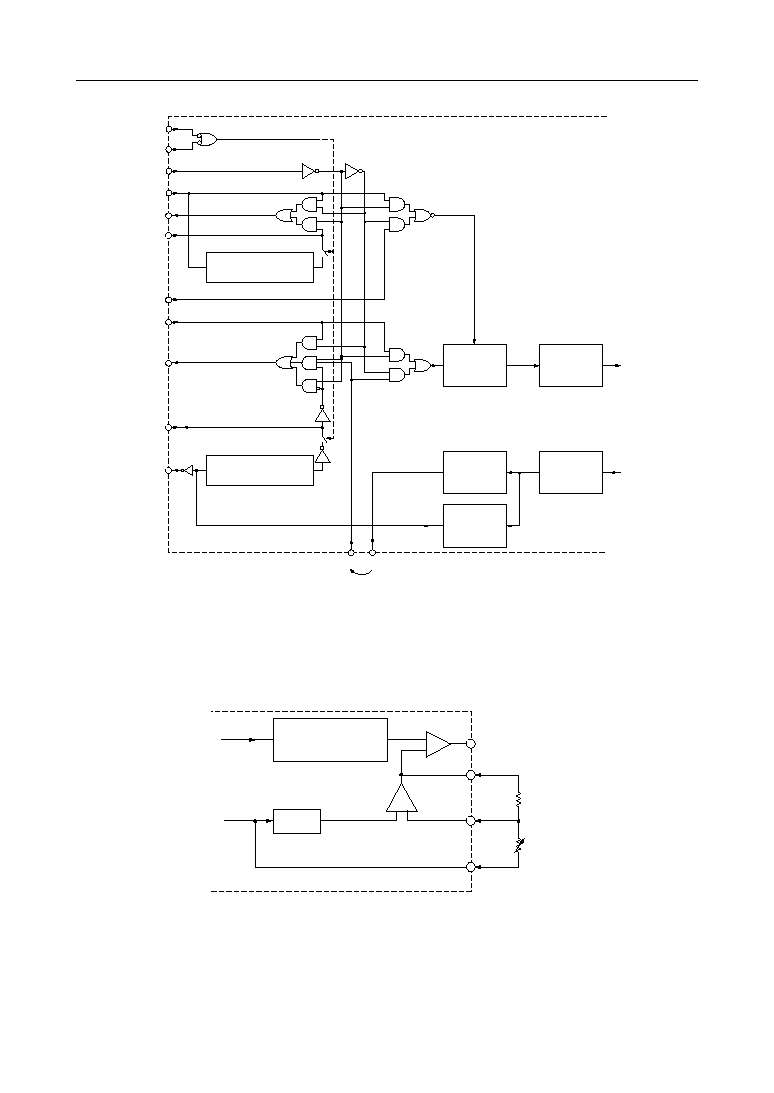
APPLICATION CIRCUIT
Notes: 1. The crystal should be wired in close physical proximity to the device.
2. High level signals should not be routed next to low level signals.
3. Bypass capacitors on V
A
, SG1, and SG2 should be as close to the device as possible.
4. AG and DG should be connected as close to the system ground as possible.
Figure 8 Application Circuit Using MSM6926RS/MSM6946RS
CLK
X
2
X
1
CC
CS
RS1
RS2
RD
Phone
Line
Crystal
LT
XD
CD1
CD2
RD1
RD2
DG
28
27
26
25
24
23
22
21
20
19
18
17
16
15
V
D
TS
1
TS
2
V
A
FT
M
AIN
AG
AO
SG1
SG2
CDR2
CDR1
DG
AG
V
A
V
D
C6
+
ORIG. MODE
ANS. MODE
Test
Data
Control
CS
RS
RD
XD
CD
V
D
C5
R
4
R
6
R
7
R
5
C0
R
2
R
3
+
≠
R
1
C3
C4
R
8
R
9
DG or V
D
V
D
C2
C1
≠
1
2
3
4
5
6
7
8
9
10
11
12
13
14
≠
+
+
≠
° Semiconductor
MSM6926/6946
20/25
25
20
21
19
SG1
AIN
AO
AG
R
4
R
6
R
7
R
5
C
0
+
≠
R
2
R
3
+
≠
R1 C2
C1
600
W : 600 W
C3
+6 dBm
0 dBm
≠6 dBm
0 dBm
≠6 dBm
Phone
Line
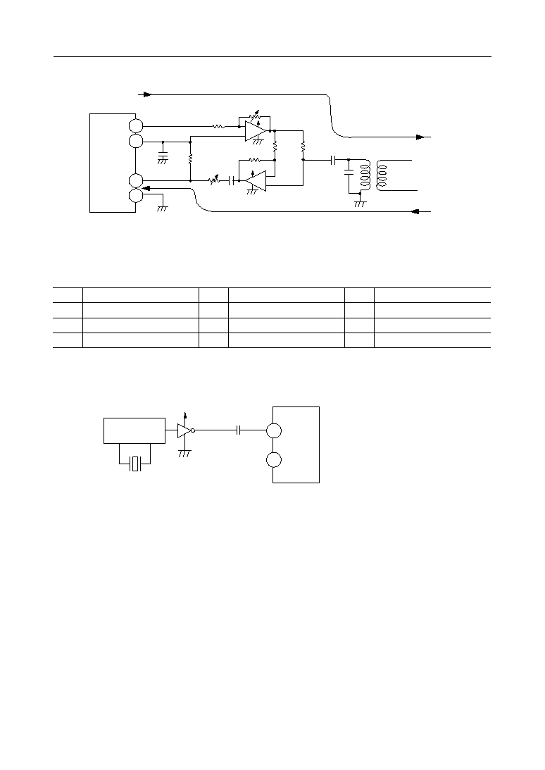
Figure 9 MSM6926RS/MSM6946RS Application
Note: The signal level on the A
IN
pin should not exceed ≠6 dBm.
C
0
, C
1
C
2
C
3
R
1
0.047
mF
2.2
mF
1
mF
600
W
R
2
R
3
R
4
R
5
51 k
W
51 k
W
51 k
W
(51 k
W) Transmit signal level
R
6
R
7
R
8
R
9
(51 k
W) Receive signal level
51 k
W
(33 k
W) Carrier detect level
51 k
W
X2
X1
External
Oscillator
V
D
*2
External Oscillator Connection
*1
*2
TTL or Hi-Speed CMOS GATE
Left unconnected
200 pF
3.58 MHz
GATE
*1
Figure 10
° Semiconductor
MSM6926/6946
21/25
(A) RS/CS delay, (B) CD/ON delay, (C) CD/OFF delay
Note: Supply voltage equals V
D
for all gates.
*: The desired delay can be realized by selecting the appropriate bits from 4020's outputs.
The number of the bits is not always 3. Each delay can be set differently from built-in delays.
Figure 11 External Delays Connection
R
CK
4020
*
(B)
R
CK
4020
*
(C)
R
CK
4020
*
(A)
V
D
V
D
RS
CD
CK
Q
Q
D
873.9 Hz
CD1
RS1
CD2
CLK
TS2
RS2
TS1
° Semiconductor
MSM6926/6946
22/25
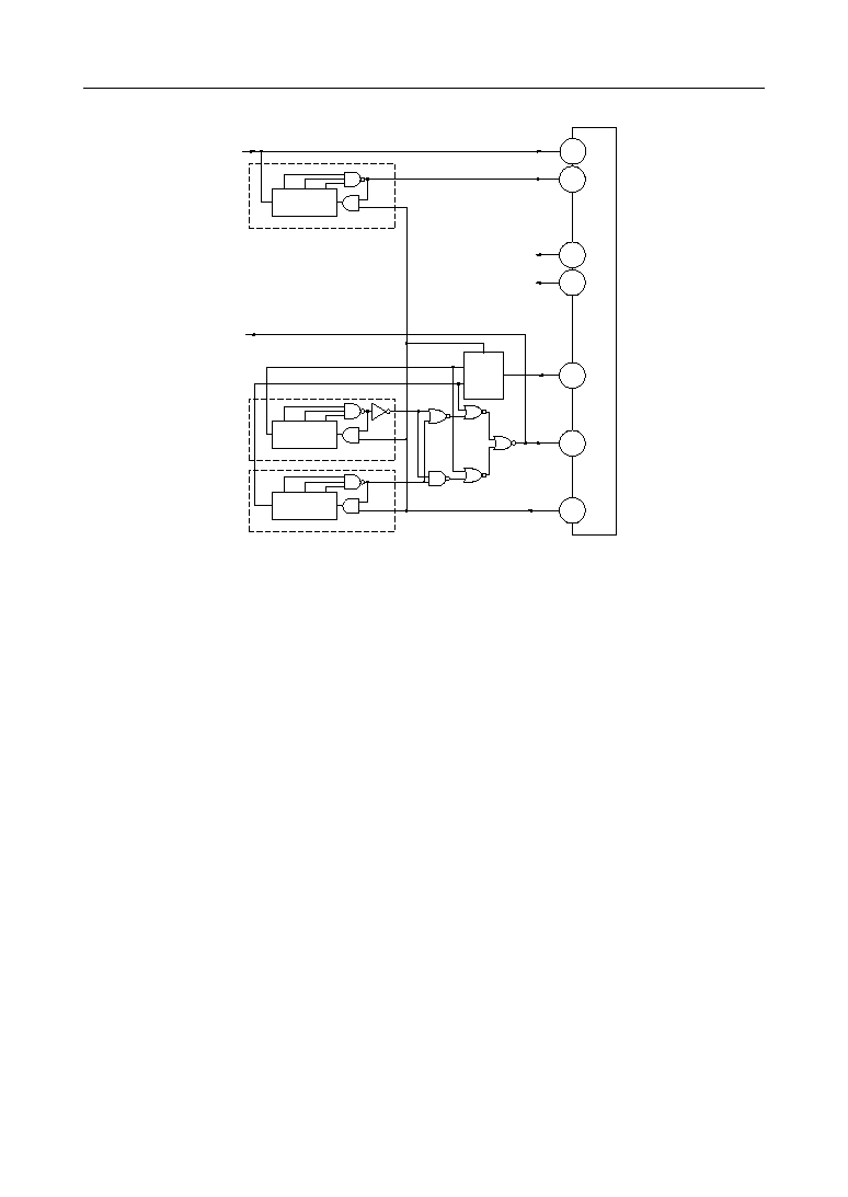
TS1
TS2
SW Control
LT
RS/CS Delay
Modulator
Transmit
Filter
De-
Modulator
Receive
Filter
Carrier
Detect
RS1
CS
RS2
CC
XD
RD
CD2
CD1
RD2 RD1
AO
AIN
Delay
CD ON
CD OFF
Figure 12 Equivalent Logic Interface of the Integrated Modem
Figure 13 External Resistor Connection for the Setting of Carrier Detect Level
R
9
CD1
CDR1
CDR2
R
8
SG2
Carrier Detect
AC/DC Converter
Carrier
SG2
V
REF
COMP
+
≠
(R8 + R9)
50 kW

° Semiconductor
MSM6926/6946
23/25
(Unit : mm)
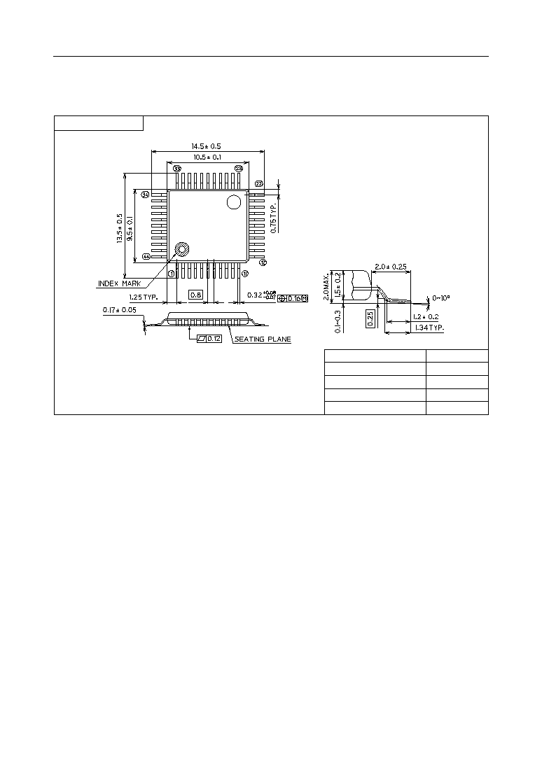
PACKAGE DIMENSIONS
DIP28-P-600-2.54
Package material
Lead frame material
Pin treatment
Solder plate thickness
Package weight (g)
Epoxy resin
42 alloy
Solder plating
5
mm or more
4.30 TYP.
° Semiconductor
MSM6926/6946
24/25
(Unit : mm)
Notes for Mounting the Surface Mount Type Package
The SOP, QFP, TSOP, SOJ, QFJ (PLCC), SHP and BGA are surface mount type packages, which
are very susceptible to heat in reflow mounting and humidity absorbed in storage.
Therefore, before you perform reflow mounting, contact Oki's responsible sales person for the
product name, package name, pin number, package code and desired mounting conditions
(reflow method, temperature and times).
QFP44-P-910-0.80-K
Package material
Lead frame material
Pin treatment
Solder plate thickness
Package weight (g)
Epoxy resin
42 alloy
Solder plating
5
mm or more
0.35 TYP.
Mirror finish
° Semiconductor
MSM6926/6946
25/25
(Unit : mm)
Notes for Mounting the Surface Mount Type Package
The SOP, QFP, TSOP, SOJ, QFJ (PLCC), SHP and BGA are surface mount type packages, which
are very susceptible to heat in reflow mounting and humidity absorbed in storage.
Therefore, before you perform reflow mounting, contact Oki's responsible sales person for the
product name, package name, pin number, package code and desired mounting conditions
(reflow method, temperature and times).
Package material
Lead frame material
Pin treatment
Solder plate thickness
Package weight (g)
Epoxy resin
42 alloy
Solder plating
5
mm or more
0.41 TYP.
QFP44-P-910-0.80-2K
Mirror finish