 | –≠–ª–µ–∫—Ç—Ä–æ–Ω–Ω—ã–π –∫–æ–º–ø–æ–Ω–µ–Ω—Ç: MSM6997H | –°–∫–∞—á–∞—Ç—å:  PDF PDF  ZIP ZIP |

° Semiconductor
MSM6996H/6996V/6997H/6997V/6998/6999
1/21
° Semiconductor
MSM6996H/6996V/6997H/6997V/6998/6999
Single Chip CODEC
GENERAL DESCRIPTION
The MSM6996H/MSM6996V/MSM6997H/MSM6997V/MSM6998/MSM6999 are a single-channel
CODEC CMOS ICs containing filters for A/D and D/A converting of the voice signal ranging from
300 Hz to 3400 Hz.
FEATURES
∑ Compliance with ITU-T companding Law
MSM6996H/MSM6996V/MSM6998 :
A-law
MSM6997H/MSM6997V/MSM6999 :
m-law
∑ Capable of independent operation of transmission and reception
∑ Transmission clock in the range of 64 kHz to 2048 kHz
∑ Adjustable transmit gain
∑ 600 W drive for analog output
MSM6996H/MSM6996V/MSM6997H/MSM6997V single end drive
MSM6998/MSM6999 Push-pull drive
∑ Built-in analog loop back fanction
MSM6996V/MSM6997V
∑ Built-in reference voltage source
∑ Low Power Dissipation (60 mW to 70 mW Typ.)
∑ Package options :
16-pin plastic DIP (DIP16-P-300-2.54)
(Product name : MSM6996HRS/MSM6997HRS)
(Product name : MSM6996VRS/MSM6997VRS)
(Product name : MSM6998RS/MSM6999RS)
16-pin cer DIP (DIP16-G-300-2.54-1)
(Product name : MSM6996HAS/MSM6997HAS)
(Product name : MSM6996VAS/MSM6997VAS)
(Product name : MSM6998AS/MSM6999AS)
24-pin plastic SOP (SOP24-P-430-1.27-K) (Product name : MSM6996HGS-K/MSM6997HGS-K)
(Product name : MSM6996VGS-K/MSM6997VGS-K)
(Product name : MSM6998GS-K/MSM6999GS-K)
E2U0010-28-81
This version: Aug. 1998
Previous version: Nov. 1996
° Semiconductor
MSM6996H/6996V/6997H/6997V/6998/6999
2/21
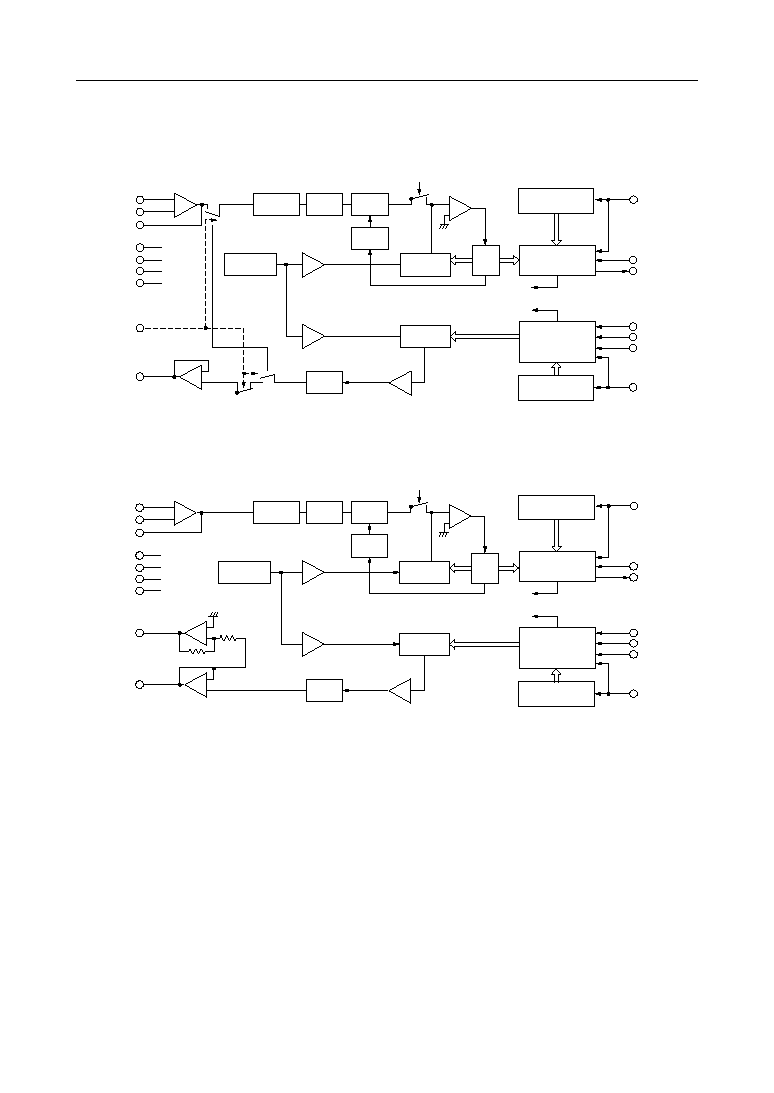
BLOCK DIAGRAM
≠
+
MSM6996H/V
MSM6997H/V
AIN+
AIN≠
GSX
V
DD
V
SS
AG
+
≠
AOUT
XSYNC
XCLOCK
PCMOUT
RCLOCK
RSYNC
PDN/BS
PCMIN
Voltage
REF.
5th
LPF
3rd
HPF
Auto
Zero
C Ladder
SAR
Receive
Controller
Transmit
Controller
R.PWD
COMP
SAMPLE
5th
LPF
≠
+
MSM6998, MSM6999
AIN+
AIN≠
GSX
V
DD
V
SS
AG
+
≠
AOUT+
Voltage
REF.
Pre Filter
5th
LPF
3rd
HPF
Auto
Zero
SAR
COMP
SAMPLE
5th
LPF
≠
+
AOUT≠
Transmit
PLL
Receive
PLL
T.PWD
*1
DG
TMC
*2
R
R
DG
XSYNC
XCLOCK
PCMOUT
RCLOCK
RSYNC
PDN/BS
PCMIN
Receive
Controller
Transmit
Controller
R.PWD
Transmit
PLL
Receive
PLL
T.PWD
*3
*
1 BS : Only MSM6997H/V
*
2 Only MSM6996V, MSM6997V
*
3 BS : Only MSM6999
Pre Filter
C Ladder
C Ladder
C Ladder
° Semiconductor
MSM6996H/6996V/6997H/6997V/6998/6999
3/21
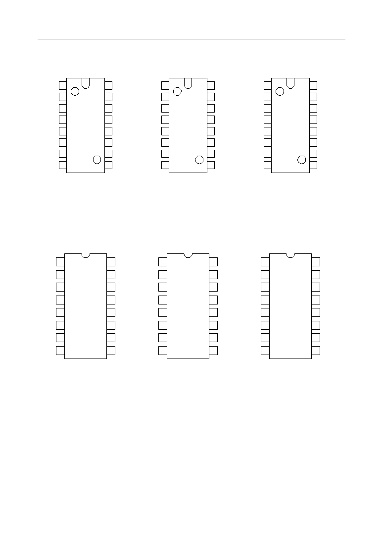
16-Pin Plastic DIP
MSM6996HRS
MSM6997HRS
16-Pin Plastic DIP
MSM6996VRS
MSM6997VRS
16-Pin Plastic DIP
MSM6998RS
MSM6999RS
1
2
3
4
5
6
7
8
9
10
11
12
13
14
15
16
AIN+
AIN≠
GSX
AG
AOUT
NC
V
DD
PCMIN
V
SS
PCMOUT
PDN/BS
DG
XSYNC
XCLOCK
RCLOCK
16-Pin Cer DIP
MSM6996HAS
MSM6997HAS
16-Pin Cer DIP
MSM6996VAS
MSM6997VAS
16-Pin Cer DIP
MSM6998AS
MSM6999AS
RSYNC
1
2
3
4
5
6
7
8
9
10
11
12
13
14
15
16
AIN+
AIN≠
GSX
AG
AOUT
TMC
V
DD
PCMIN
V
SS
PCMOUT
PDN/BS
DG
XSYNC
XCLOCK
RCLOCK
RSYNC
1
2
3
4
5
6
7
8
9
10
11
12
13
14
15
16
AIN+
AIN≠
GSX
AG
AOUT+
AOUT≠
V
DD
PCMIN
V
SS
PCMOUT
PDN/BS
DG
XSYNC
XCLOCK
RCLOCK
RSYNC
1
2
3
4
5
6
7
8
9
10
11
12
13
14
15
16
1
2
3
4
5
6
7
8
9
10
11
12
13
14
15
16
1
2
3
4
5
6
7
8
9
10
11
12
13
14
15
16
AIN+
AIN≠
GSX
AG
AOUT
NC
V
DD
PCMIN
V
SS
PCMOUT
PDN/BS
DG
XSYNC
XCLOCK
RCLOCK
RSYNC
AIN+
AIN≠
GSX
AG
AOUT
TMC
V
DD
PCMIN
V
SS
PCMOUT
PDN/BS
DG
XSYNC
XCLOCK
RCLOCK
RSYNC
AIN+
AIN≠
GSX
AG
AOUT+
AOUT≠
V
DD
PCMIN
V
SS
PCMOUT
PDN/BS
DG
XSYNC
XCLOCK
RCLOCK
RSYNC
PIN CONFIGURATION (TOP VIEW)
NC : No connect pin
NC : No connect pin
° Semiconductor
MSM6996H/6996V/6997H/6997V/6998/6999
4/21
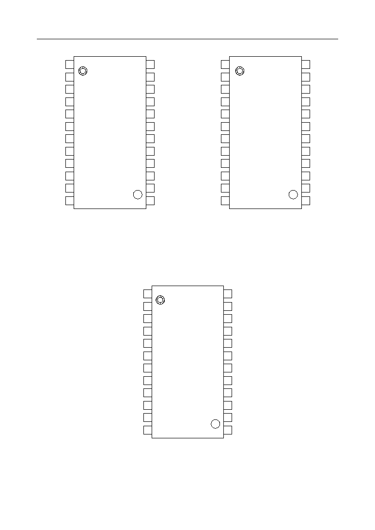
24-Pin Plastic SOP
MSM6996HGS-K
MSM6997HGS-K
1
2
3
4
5
6
7
8
9
10
11
12
13
14
15
16
17
18
19
20
21
22
23
24
AIN+
AIN≠
GSX
AG
AOUT
V
SS
PCMOUT
PDN/BS
DG
XSYNC
RSYNC
24-Pin Plastic SOP
MSM6996VGS-K
MSM6997VGS-K
V
DD
PCMIN
XCLOCK
RCLOCK
24-Pin Plastic SOP
MSM6998GS-K
MSM6999GS-K
AG
1
2
3
4
5
6
7
8
9
10
11
12
13
14
15
16
17
18
19
20
21
22
23
24
AIN+
AIN≠
GSX
AG
AOUT
TMC
V
SS
PCMOUT
PDN/BS
DG
XSYNC
RSYNC
V
DD
PCMIN
XCLOCK
RCLOCK
AG
1
2
3
4
5
6
7
8
9
10
11
12
13
14
15
16
17
18
19
20
21
22
23
24
AIN+
AIN≠
GSX
AG
AOUT+
AOUT≠
V
SS
PCMOUT
PDN/BS
DG
XSYNC
RSYNC
V
DD
PCMIN
XCLOCK
RCLOCK
AG
NC
NC
NC
NC
NC
NC
NC
NC
NC
NC
NC
NC
NC
NC
NC
NC
NC
NC
NC
NC
NC
NC
NC : No connect pin
NC : No connect pin
NC : No connect pin
° Semiconductor
MSM6996H/6996V/6997H/6997V/6998/6999
5/21
PIN AND FUNCTIONAL DESCRIPTIONS
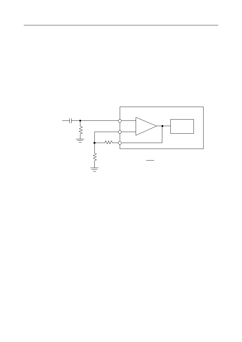
AIN+, AIN≠, GSX
These three pins are used for the transmit level adjustment.
AIN+ is a non-inverting analog input pin which is connected to the non-inverting input of a transmit
amplifier.
AIN≠ is an inverting analog input pin which is connected to the inverting input of the transmit
amplifier.
GSX is a transmit amplifier output pin.
Adjustment can be done by following method.
R2
+
≠
AIN≠
Gain = 1 +
AIN+
GSX
RC
Active
Filter
Analog
Input
R3
R1
C1
R2
R3
AG
< 10
Notes: 1. R
2
+ R
3
> 10 kW
2. When the DC off-set voltage of analog input is more than 20 mV, C1 and R1 should
provide for DC blocking.
In this case, cut-off frequency of HPF, composed by R
1
and C
1
, should be less than 30 Hz.
3. R
1
should be less than 20 kW
AG
AG is an analog ground.
AG is connected to the analog system ground.
AOUT
AOUT is the analog signal output pin for the MSM6996H/V and MSM6997H/V.
The output voltage range is 5 V
PP
. This output can drive the 600 W resistor.
AOUT+, AOUT≠
Analog output for the MSM6998 and MSM6999.
The output signal amplitudes are 5 V
PP
. The AOUT≠ output is inverted to the AOUT+ output. These
outputs can drive a 600 W impedance.
V
DD
V
DD
is the positive power supply.
The voltage supplied to this pin should be +5 V
±
5%.