
° Semiconductor
MSM6996H/6996V/6997H/6997V/6998/6999
1/21
° Semiconductor
MSM6996H/6996V/6997H/6997V/6998/6999
Single Chip CODEC
GENERAL DESCRIPTION
The MSM6996H/MSM6996V/MSM6997H/MSM6997V/MSM6998/MSM6999 are a single-channel
CODEC CMOS ICs containing filters for A/D and D/A converting of the voice signal ranging from
300 Hz to 3400 Hz.
FEATURES
∑ Compliance with ITU-T companding Law
MSM6996H/MSM6996V/MSM6998 :
A-law
MSM6997H/MSM6997V/MSM6999 :
m-law
∑ Capable of independent operation of transmission and reception
∑ Transmission clock in the range of 64 kHz to 2048 kHz
∑ Adjustable transmit gain
∑ 600 W drive for analog output
MSM6996H/MSM6996V/MSM6997H/MSM6997V single end drive
MSM6998/MSM6999 Push-pull drive
∑ Built-in analog loop back fanction
MSM6996V/MSM6997V
∑ Built-in reference voltage source
∑ Low Power Dissipation (60 mW to 70 mW Typ.)
∑ Package options :
16-pin plastic DIP (DIP16-P-300-2.54)
(Product name : MSM6996HRS/MSM6997HRS)
(Product name : MSM6996VRS/MSM6997VRS)
(Product name : MSM6998RS/MSM6999RS)
16-pin cer DIP (DIP16-G-300-2.54-1)
(Product name : MSM6996HAS/MSM6997HAS)
(Product name : MSM6996VAS/MSM6997VAS)
(Product name : MSM6998AS/MSM6999AS)
24-pin plastic SOP (SOP24-P-430-1.27-K) (Product name : MSM6996HGS-K/MSM6997HGS-K)
(Product name : MSM6996VGS-K/MSM6997VGS-K)
(Product name : MSM6998GS-K/MSM6999GS-K)
E2U0010-28-81
This version: Aug. 1998
Previous version: Nov. 1996
° Semiconductor
MSM6996H/6996V/6997H/6997V/6998/6999
2/21
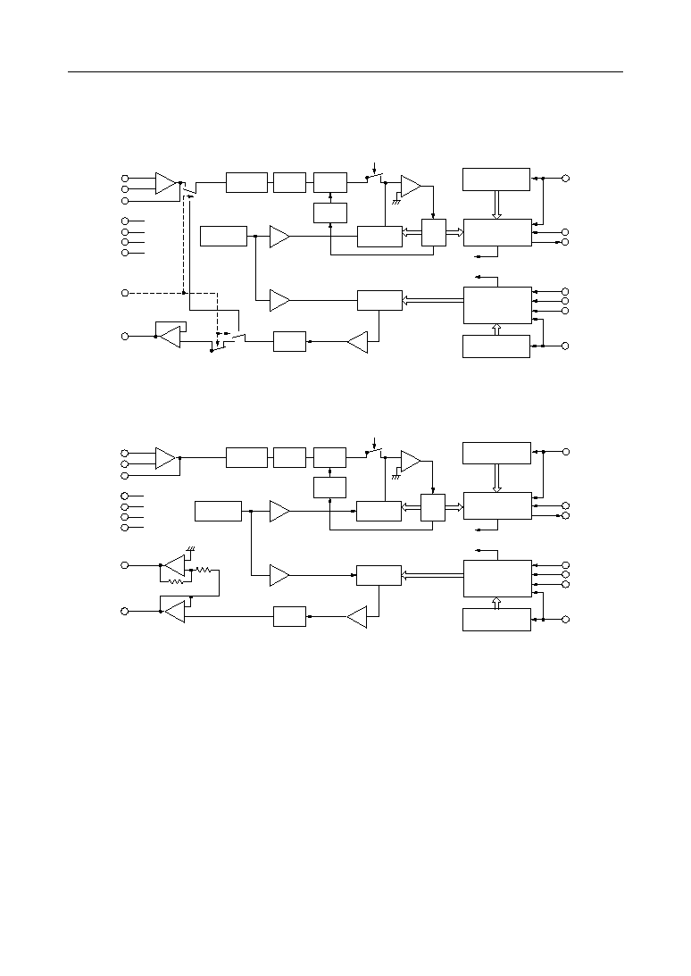
BLOCK DIAGRAM
≠
+
MSM6996H/V
MSM6997H/V
AIN+
AIN≠
GSX
V
DD
V
SS
AG
+
≠
AOUT
XSYNC
XCLOCK
PCMOUT
RCLOCK
RSYNC
PDN/BS
PCMIN
Voltage
REF.
5th
LPF
3rd
HPF
Auto
Zero
C Ladder
SAR
Receive
Controller
Transmit
Controller
R.PWD
COMP
SAMPLE
5th
LPF
≠
+
MSM6998, MSM6999
AIN+
AIN≠
GSX
V
DD
V
SS
AG
+
≠
AOUT+
Voltage
REF.
Pre Filter
5th
LPF
3rd
HPF
Auto
Zero
SAR
COMP
SAMPLE
5th
LPF
≠
+
AOUT≠
Transmit
PLL
Receive
PLL
T.PWD
*1
DG
TMC
*2
R
R
DG
XSYNC
XCLOCK
PCMOUT
RCLOCK
RSYNC
PDN/BS
PCMIN
Receive
Controller
Transmit
Controller
R.PWD
Transmit
PLL
Receive
PLL
T.PWD
*3
*
1 BS : Only MSM6997H/V
*
2 Only MSM6996V, MSM6997V
*
3 BS : Only MSM6999
Pre Filter
C Ladder
C Ladder
C Ladder
° Semiconductor
MSM6996H/6996V/6997H/6997V/6998/6999
3/21
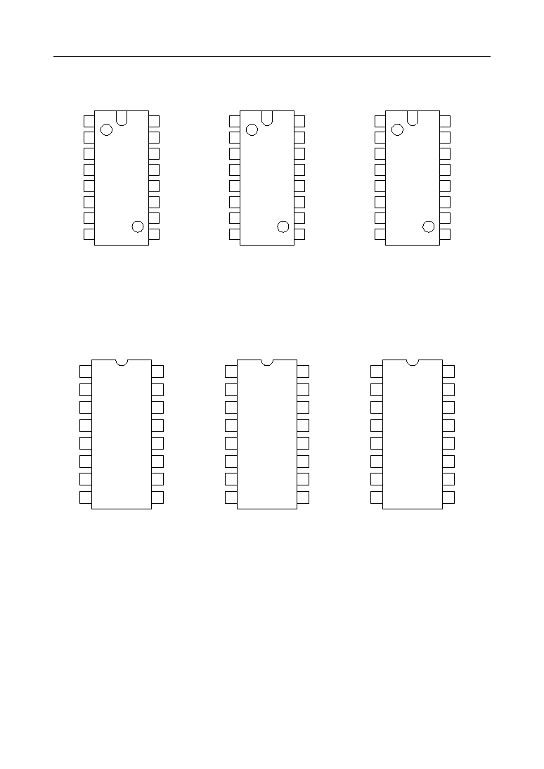
16-Pin Plastic DIP
MSM6996HRS
MSM6997HRS
16-Pin Plastic DIP
MSM6996VRS
MSM6997VRS
16-Pin Plastic DIP
MSM6998RS
MSM6999RS
1
2
3
4
5
6
7
8
9
10
11
12
13
14
15
16
AIN+
AIN≠
GSX
AG
AOUT
NC
V
DD
PCMIN
V
SS
PCMOUT
PDN/BS
DG
XSYNC
XCLOCK
RCLOCK
16-Pin Cer DIP
MSM6996HAS
MSM6997HAS
16-Pin Cer DIP
MSM6996VAS
MSM6997VAS
16-Pin Cer DIP
MSM6998AS
MSM6999AS
RSYNC
1
2
3
4
5
6
7
8
9
10
11
12
13
14
15
16
AIN+
AIN≠
GSX
AG
AOUT
TMC
V
DD
PCMIN
V
SS
PCMOUT
PDN/BS
DG
XSYNC
XCLOCK
RCLOCK
RSYNC
1
2
3
4
5
6
7
8
9
10
11
12
13
14
15
16
AIN+
AIN≠
GSX
AG
AOUT+
AOUT≠
V
DD
PCMIN
V
SS
PCMOUT
PDN/BS
DG
XSYNC
XCLOCK
RCLOCK
RSYNC
1
2
3
4
5
6
7
8
9
10
11
12
13
14
15
16
1
2
3
4
5
6
7
8
9
10
11
12
13
14
15
16
1
2
3
4
5
6
7
8
9
10
11
12
13
14
15
16
AIN+
AIN≠
GSX
AG
AOUT
NC
V
DD
PCMIN
V
SS
PCMOUT
PDN/BS
DG
XSYNC
XCLOCK
RCLOCK
RSYNC
AIN+
AIN≠
GSX
AG
AOUT
TMC
V
DD
PCMIN
V
SS
PCMOUT
PDN/BS
DG
XSYNC
XCLOCK
RCLOCK
RSYNC
AIN+
AIN≠
GSX
AG
AOUT+
AOUT≠
V
DD
PCMIN
V
SS
PCMOUT
PDN/BS
DG
XSYNC
XCLOCK
RCLOCK
RSYNC
PIN CONFIGURATION (TOP VIEW)
NC : No connect pin
NC : No connect pin
° Semiconductor
MSM6996H/6996V/6997H/6997V/6998/6999
4/21
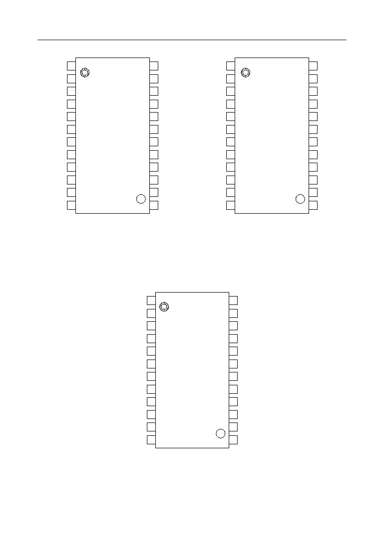
24-Pin Plastic SOP
MSM6996HGS-K
MSM6997HGS-K
1
2
3
4
5
6
7
8
9
10
11
12
13
14
15
16
17
18
19
20
21
22
23
24
AIN+
AIN≠
GSX
AG
AOUT
V
SS
PCMOUT
PDN/BS
DG
XSYNC
RSYNC
24-Pin Plastic SOP
MSM6996VGS-K
MSM6997VGS-K
V
DD
PCMIN
XCLOCK
RCLOCK
24-Pin Plastic SOP
MSM6998GS-K
MSM6999GS-K
AG
1
2
3
4
5
6
7
8
9
10
11
12
13
14
15
16
17
18
19
20
21
22
23
24
AIN+
AIN≠
GSX
AG
AOUT
TMC
V
SS
PCMOUT
PDN/BS
DG
XSYNC
RSYNC
V
DD
PCMIN
XCLOCK
RCLOCK
AG
1
2
3
4
5
6
7
8
9
10
11
12
13
14
15
16
17
18
19
20
21
22
23
24
AIN+
AIN≠
GSX
AG
AOUT+
AOUT≠
V
SS
PCMOUT
PDN/BS
DG
XSYNC
RSYNC
V
DD
PCMIN
XCLOCK
RCLOCK
AG
NC
NC
NC
NC
NC
NC
NC
NC
NC
NC
NC
NC
NC
NC
NC
NC
NC
NC
NC
NC
NC
NC
NC : No connect pin
NC : No connect pin
NC : No connect pin
° Semiconductor
MSM6996H/6996V/6997H/6997V/6998/6999
5/21
PIN AND FUNCTIONAL DESCRIPTIONS
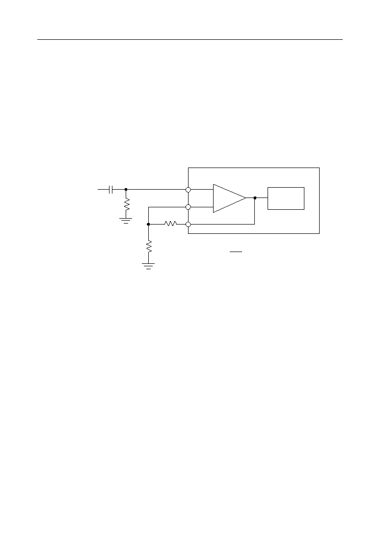
AIN+, AIN≠, GSX
These three pins are used for the transmit level adjustment.
AIN+ is a non-inverting analog input pin which is connected to the non-inverting input of a transmit
amplifier.
AIN≠ is an inverting analog input pin which is connected to the inverting input of the transmit
amplifier.
GSX is a transmit amplifier output pin.
Adjustment can be done by following method.
R2
+
≠
AIN≠
Gain = 1 +
AIN+
GSX
RC
Active
Filter
Analog
Input
R3
R1
C1
R2
R3
AG
< 10
Notes: 1. R
2
+ R
3
> 10 kW
2. When the DC off-set voltage of analog input is more than 20 mV, C1 and R1 should
provide for DC blocking.
In this case, cut-off frequency of HPF, composed by R
1
and C
1
, should be less than 30 Hz.
3. R
1
should be less than 20 kW
AG
AG is an analog ground.
AG is connected to the analog system ground.
AOUT
AOUT is the analog signal output pin for the MSM6996H/V and MSM6997H/V.
The output voltage range is 5 V
PP
. This output can drive the 600 W resistor.
AOUT+, AOUT≠
Analog output for the MSM6998 and MSM6999.
The output signal amplitudes are 5 V
PP
. The AOUT≠ output is inverted to the AOUT+ output. These
outputs can drive a 600 W impedance.
V
DD
V
DD
is the positive power supply.
The voltage supplied to this pin should be +5 V
±
5%.
° Semiconductor
MSM6996H/6996V/6997H/6997V/6998/6999
6/21
PCMIN
PCM signal input.
The serial input PCM signal is converted from digital to analog, synchronizing with the synchronous
signal RSYNC and clock signal RCLOCK.
The data rate of PCM signal ranges from 64 kbps to 2048 kbps.
The PCM signal is read at the falling edge of the clock signal and latched into the internal register
when finished to read eight bits data.
The top of the PCM data is specified by RSYNC pulse timing.
RCLOCK
Receive clock pulse input.
The frequency of this clock pulse should be identified with the data rate of PCM input signal at the
PCMIN pin.
This RCLOCK signal can be a continuous clock or a burst clock with nine bits or more.
In the case of a burst clock, input the following timing.
XCLOCK
Transmit clock input.
The PCM output data rate from the PCMOUT pin is set by this clock frequency.
The applicable clock frequencies range from 64 kHz to 2048 kHz.
This XCLOCK signal can be a continuous clock or a burst clock with nine bits or more.
In the case of a burst clock, input the following timing.
1
2
3
4
5
6
7
8
9
MSD
D2
D3
D4
D5
D6
D7
D8
PCMOUT
XCLOCK
XSYNC
9 Clocks are required
1
2
3
4
5
6
7
8
9
MSD
D2
D3
D4
D5
D6
D7
D8
PCMIN
RCLOCK
RSYNC
9 Clocks are required

° Semiconductor
MSM6996H/6996V/6997H/6997V/6998/6999
7/21
RSYNC
Receive synchronizing signal input.
Eight required bits are selected from serial PCM signals on the PCMIN pin by the receive
synchronizing signal.
The whole timing signal in the receive section are synchronize by this synchronizing signal.
This signal must be synchronize in phase with RCLOCK.
The frequency should be 8 kHz
±
50 ppm to guarantee the AC characteristics of receive section.
However, same as the RCLOCK frequency, this device can operate in the range of 8 kHz
±
2 kHz, with
no guarantee of adherence to the electrical characteristics in this specification as a catalogue value.
Fixing this signal to logic "1" or "0", the receive circuit is driver in a power down state.
XSYNC
Transmit synchronizing signal input.
The PCM output signal from the PCMOUT pin is output in synchronization with this transmit
synchronizing signal.
All transmit timing signals are triggered to synchronize with this signal. This signal should be
synchronized in phase with XCLOCK pulse.
The frequency should be 8 kHz
±
50 ppm to guarantee the AC characteristics of transmit section.
Fixing this signal to logic "1" or "0", the transmit circuit is driver in a power down state.
DG
Ground of digital signal.
This pin is electrically separated from the AG pin in this device.
The DG pin must be connected to the AG pin on the printed circuit board to make common to the
AG pin.
PDN/BS
Power down signal input.
When this input is held at low level more than 1 ms, the device is put into the power-down mode.
PCMOUT
PCM signal output.
The PCM output signal is output in synchronization with the rising edge of XCLOCK pulse orderly
from MSD first. (The first bit of the PCM signal may output at the rising edge of XSYNC pulse,
according to the timing of XSYNC and XCLOCK pulse.). During the PCMOUT signal output except
the 8-bit pulses, the pin is in an open state, therefore, multiple connections by wired-OR are easily
possible at this pin.
The code companding law and output code format depend on ITU-T Recommendation G.711, and
for the MSM6996H, MSM6996V, and MSM6998 (A-law) the output PCM signals are obtained by
inverting the even bits of signals.
Input/Output
Level
+Full scale
+0
≠0
≠Full scale
PCMIN/PCMOUT
MSM6996 (A-law)
MSM6997 (
m-law)
1
0
1
0
1
0
1
0
1
1
0
1
0
1
0
1
0
1
0
1
0
1
0
1
0
0
1
0
1
0
1
0
1
0
0
0
0
0
0
0
1
1
1
1
1
1
1
1
0
1
1
1
1
1
1
1
0
0
0
0
0
0
0
0
MSM6998 (A-law)
MSM6999 (
m-law)
° Semiconductor
MSM6996H/6996V/6997H/6997V/6998/6999
8/21
≠
+
AIN
AOUT
TRANSMIT
BPF
PCMOUT
PCMIN
AD
RECV
LPF
DA
≠
+
AG
Signal flow in normal operating mode
Signal flow in analog loop-back mode
V
SS
Negative voltage power supply.
The range of power supply voltage is ≠5 V
±
5%.
TMC
Control signal input for mode selection.
This pin select the normal operating mode or analog loop-back mode.
TMC Input
Mode
> 2.0 V
Normal operation
< 0.8 V
Analog loop-back
° Semiconductor
MSM6996H/6996V/6997H/6997V/6998/6999
9/21
ABSOLUTE MAXIMUM RATINGS
RECOMMENDED OPERATING CONDITIONS
* : The value for the MSM6997 and MSM6999
Parameter
Power Supply Voltage
Analog Input Voltage
Digital Input Voltage
Storage Temperature
Symbol
V
DD
V
AIN
V
DIN
T
STG
Rating
0 to 7
V
DD
≠0.3 to V
DD
+ 0.3
≠0.3 to V
DD
+ 0.3
≠55 to +150
Unit
V
V
V
∞C
V
SS
≠7 to 0
V
Condition
--
--
--
--
--
(Ta = 0∞C to 70∞C)
Parameter
Symbol
Condition
Min.
Typ.
Max.
Unit
Power Supply Voltage
Analog Input Voltage
V
DD
V
SS
V
AIN
Input High Voltage
Input Low Voltage
V
IH
V
IL
--
--
Connect AIN≠ and GSX
XSYNC, XCLOCK, PCMIN,
RSYNC, RCLOCK, TMC, PDN/BS
4.75
5
5.25
V
≠5.25
≠5
≠4.75
V
--
--
5
V
P-P
2.0
--
V
DD
V
0
--
0.8
V
Clock Frequency
f
C
XCLOCK, RCLOCK
kHz
--
Sync Pulse Frequency
f
S
XSYNC, RSYNC
--
8
--
kHz
Clock Duty Ratio
D
L
XCLOCK, RCLOCK
40
50
60
%
Digital Input Rise Time
t
Ir
--
--
50
ns
Digital Input Fall Time
t
If
--
--
50
ns
XSYNC, XCLOCK, PCMIN,
RSYNC, RCLOCK (Fig. 1)
Transmit Sync Timing
t
XS
50
--
--
ns
t
SX
100
--
--
ns
XCLOCK∆XSYNC (Fig. 2)
XSYNC∆XCLOCK (Fig. 2)
Receive Sync Timing
t
RS
50
--
--
ns
t
SR
100
--
--
ns
RCLOCK∆RSYNC (Fig. 2)
RSYNC∆RCLOCK (Fig. 2)
t
WX
1/fc
--
--
m
s
--
t
WR
1/fc
--
--
m
s
--
Transmit Sync Pulse Width
Receive Sync Pulse Width
t
DS
100
--
--
ns
--
t
DH
100
--
--
ns
--
PCMIN Set-up Time
PCMIN Hold Time
t
BS
200
--
--
ns
--
BS Set-up Time *
t
BH
200
--
--
ns
--
BS Hold Time *
R
AL
600
--
--
W
Analog Output Load
C
AL
--
--
100
pF
R
DL
1
--
--
kW
Digital Output Load
C
DL
--
--
100
pF
AOUT, AOUT+, AOUT≠
--
V
IO
≠200
--
+200
Allowable Analog Input
Offset Voltage
Transmit gain stage, Gain = 1
64
2048
mV
≠20
--
+20
Transmit gain stage, Gain = 10
10
--
--
kW
GSK
--
Operating Temperature
Ta
∞C
--
0
25
70
° Semiconductor
MSM6996H/6996V/6997H/6997V/6998/6999
10/21
ELECTRICAL CHARACTERISTICS
DC and Digital Interface Characteristics
* : The upper is specified for the MSM6996/MSM6997 and the lower for the MSM6998/MSM6999
(V
DD
= +5 V ±5%, V
SS
= ≠5 V ±5%, Ta = 0∞C to 70∞C)
Parameter
Symbol
Condition
Min.
Typ.
Max.
Unit
Power Supply Current
Power Supply Current
(Stand-by)
I
DD1
I
SS1
I
DD2
I
SS2
Input High Voltage
V
IH
XCLOCK, RCLOCK
2048 kHz
--
--
7.0
12
mA
--
6.5
12
--
--
3.0
mA
--
--
1.5
2.2
--
--
V
Input Low Voltage
V
IL
V
I
IH
--
< 0.5
2.0
m
A
Input Leakage Current
I
IL
--
< 0.2
0.5
Output Leakage Current
I
OH
--
< 5
10
m
A
Analog Output Offset Voltage
V
OFF
≠150
0
+150
mV
--
Input Capacitance
C
IN
--
5
--
pF
--
R
IN
--
1
--
MW
f
IN
< 3.4 kHz
Analog Input Resistance
(Operating)
--
--
0.8
--
0.1
0.4
V
Output Low Voltage
V
OL
*
14
14
*
° Semiconductor
MSM6996H/6996V/6997H/6997V/6998/6999
11/21
AC Characteristics
Parameter
Transmit Frequency Response
Symbol
L
OSS
T1
Level
60
Min.
20
Typ.
--
Max.
--
Unit
(V
DD
= +5 V ±5%, V
SS
= ≠5 V ±5%, Ta = 0∞C to 70∞C)
Freq.
Condition
L
OSS
T2
300
≠0.15
--
+0.25
L
OSS
T3
820
Reference
dB
0
L
OSS
T4
2020
≠0.15
--
+0.25
L
OSS
T5
3000
≠0.15
--
+0.25
L
OSS
T6
3400
0
--
0.8
Receive Frequency Response
L
OSS
R1
300
≠0.1
--
+0.2
L
OSS
R2
820
Reference
L
OSS
R3
2020
≠0.1
--
+0.2
dB
0
L
OSS
R4
3000
≠0.1
--
+0.2
L
OSS
R5
3400
0
--
0.8
Transmit Signal to Noise
SD T1
36
--
--
3
SD T2
36
--
--
0
SD T3
36
--
--
≠30
SD T4
1020
31
--
--
dB
≠40
SD T5
26
--
--
≠45
SD R1
36
--
--
3
SD R2
36
--
--
0
SD R3
36
--
--
≠30
SD R4
1020
31
--
--
dB
≠40
SD R5
26
--
--
≠45
(dBm0)
(Hz)
Ratio *1
Receive Signal to Noise
Ratio *1
or
or
820
820
Transmit Gain Tracking
GT T1
≠0.2
--
+0.2
1020
Reference
dB
3
≠0.2
--
+0.2
≠0.4
--
+0.4
≠0.8
--
+0.8
Receive Gain Tracking
GT R1
≠0.2
--
+0.2
GT R2
Reference
GT R3
1020
≠0.2
--
+0.2
GT R4
≠0.4
--
+0.4
GT R5
≠0.8
--
+0.8
GT T2
GT T3
GT T4
GT T5
≠10
≠40
≠50
≠55
3
≠10
≠40
≠50
≠55
or
or
820
820
dB
Note: *1 The measurement is taken with P-message filter
° Semiconductor
MSM6996H/6996V/6997H/6997V/6998/6999
12/21
AC Characteristics (Continued)
Parameter
Symbol
Level
Min.
Typ.
Max.
Unit
(V
DD
= +5 V ±5%, V
SS
= ≠5 V ±5%, Ta = 0∞C to 70∞C)
Freq.
Condition
Idle Channel
N
IDL
T
--
--
≠75
--
N
IDL
R
--
--
≠75
--
t
GD
T1
--
--
0.75
0
500
--
--
0.35
ms
--
--
0.125
t
GD
R1
--
--
0.75
t
GD
R2
--
--
0.35
t
GD
R3
--
--
0.125
ms
t
GD
R4
--
--
0.125
(dBm0)
(Hz)
Noise
*1
Transmit Group Delay Time
*3
--
Transmit
Receive
dBmOp
Absolute Gain
*2
AV T
≠0.5
0
+0.5
0
AV R
≠0.5
0
+0.5
0
1020 or 820
Transmit
Receive
dB
1020 or 820
t
D
--
--
0.52
0
--
ms
Absolute Delay Time
t
GD
T2
600
t
GD
T3
1000
t
GD
T4
2600
t
GD
T5
2800
--
--
--
0.75
t
GD
R5
--
--
0.75
500
600
1000
2600
2800
0
Receive Group Delay Time
*3
--
0.125
Crosstalk Attenuation
C
R
T
--
--
66
C
R
R
--
--
66
--
1020 or 820
T to R
R to T
dB
1020 or 820
Out-of-Band Spurious
S
--
--
≠30
0
dBmO
300 to 3400
IMD 1
--
--
≠35
≠4
dBmO
f
a
= 470
Intermodulation Distortion
f
b
= 320
V
DD
Noise Rejection
PPSR T
--
30
--
PPSR R
--
30
--
Transmit
Receive
dB
V
SS
Noise Rejection
NPSR T
--
30
--
NPSR R
--
30
--
200
Transmit
Receive
0 to 300
mVp-p
Ratio
Ratio
--
kHz
Discrimination
DIS
30
--
--
0
dB
4.6 kHz to
72 kHz
t
DO
20
100
R
DL
= 2 kW
t
SD
t
XD1
t
XD2
t
XD3
50
150
300
50
100
300
50
100
300
50
180
300
ns
Digital Output Delay Time
Digital Output Fall Time
--
ns
C
DL
= 100 pF
Notes: *1 The measurement is taken with P-message filter
*2 MSM6996/MSM6998 0 dB = 1.231 Vrms
MSM6997/MSM6999 0 dB = 1.227 Vrms
*3 Reference : 1800 Hz
° Semiconductor
MSM6996H/6996V/6997H/6997V/6998/6999
13/21
TIMING DIAGRAM
Wave Time Measurement Level
t
WX
t
Ir
t
If
t
DOf
2.4 V
1.4 V
0.4 V
Note: Timing between signal waves is judged at 1.4 V
2.4 V
1.4 V
0.4 V
t
WR
Basic Timing
XCLOCK
t
XS
t
XD1
1
2
3
4
5
6
7
8
9
10
1
2
3
4
5
6
7
8
9
10
t
XD2
t
XD3
t
SX
1/f
C
t
WX
t
SD
MSD
D2
D3
D4
D5
D6
D7
D8
t
RS
t
SR
t
WR
t
DS
t
DH
Transmitter
Section
Receiver
Section
XSYNC
PCMOUT
RCLOCK
RSYNC
Note 1):
When t
XS
£ 1/2 • fc, the Delay of the MSD bit is defined as t
XD1
.
When t
SX
£ 1/2 • fc, the Delay of the MSD bit is defined as t
SD
.
Note 2):
Transmit synchronizing and clock pulse, and Receive synchronizing and clock pulse may be
asynchronous mutually.
Note 3):
The threshold level is 1.4 V.
t
DS
t
DH
PCMIN
,
D8
,
D7
D6
D5
,
D4
D3
D2
,
MSD
,
Invalid Data
,
Figure 1
Figure 2
° Semiconductor
MSM6996H/6996V/6997H/6997V/6998/6999
14/21
RSYNC
Allowable Range
8 Bits Decode
7 Bits Decode
8 Bits Decode
1 2 3 4 5 6 7 8
1 2 3 4 5 6 7 8
1 2 3 4 5 6 7 8
1 2 3 4 5 6 7 8 9
1 2 3 4 5 6 7 8 9
1 2 3 4 5 6 7 8 9
Disable
t
BS
t
BH
PCMIN
RCLOCK
BS
Decoder
Operation
Notes: Follow these procedures when the Bit-steal function is used:
1. Set the RSYNC pin to OFF ("L") after the PDN/BS pin is set at "H" for 10ms or more.
2. Set the RSYNC to ON after a pulse is input at the PDN/BS pin.
3. The Bit-steal function starts to operate.
more than 10ms
~
RSYNC
PCMIN
RCLK
,,,,
,,,,
more than 10ms
PDN/BS
125
m
s
~
~ ~
~ ~
~ ~
~ ~
~ ~
Timing for 7 bits Decode (Specified for MSM6997/6999)
Figure 3
Timing for Bit-steal Function Setting
° Semiconductor
MSM6996H/6996V/6997H/6997V/6998/6999
15/21
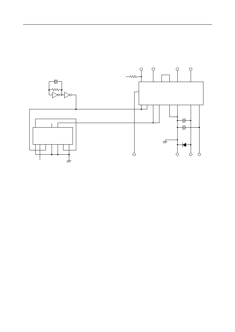
APPLICATION CIRCUIT
Basic Circuit
Notes: 1. Insert diode for preventing from Latch-Up at turn on Power.
Recommended Diode Specification.
∑ High Speed Switching
∑ Allowerable Power dissipation 250 mW to 300 mW
∑ Forward Voltage Drop < 1.3 V (at 100 mA)
2. AG and DG must be connected in the printed circuit board mounted this device, for
preventing from Latch-Up.
2 kW
IN
OUT
X R
X
R
DG
AG
V
SS
V
DD
+
≠
OUT
IN
≠
+
PCM
ANALOG
+5 V
Note 1
0 V
≠5 V +5 V
Power Down
1 : NOR
0 : Power Down
R E C
R
E C
15 10 9
8
7
2
1
16 6
+5 V
14
+5 V
Q4
Q4
10 M
XTAL
2.048 MHz
4049
4049
AIN+
AOUT
PDN/BS
IN
OUT
M4520RS
GSX AIN≠
10 mF
10 mF
CLOCK SYNC
DG
° Semiconductor
MSM6996H/6996V/6997H/6997V/6998/6999
16/21
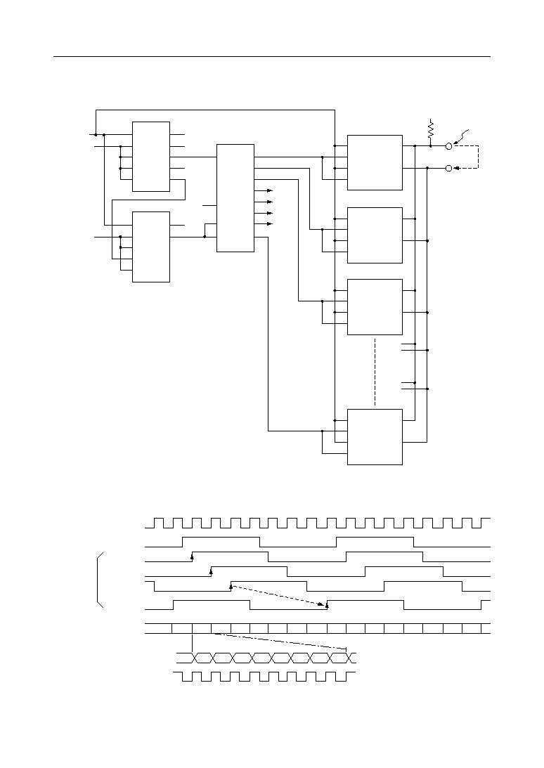
Example of Multi-Channel Connections (8ch)
8
7
No.1
2
3
4
5
6
7
8 No.1 2
3
4
5
6
7 8
MSD
LSD
Q
C
Output
Q
B
Output
Q
A
Q
B
Q
C
Q
H
Multiple PCM
512K CLK
74161(1)
74161(2)
74164
Output
Example of Multi-Channel Timing
CK
Q
A
1 kW
+5 V
Multiple
PCM
XC
PCM
OUT
PCM
IN
CLR Q
B
E
P
Q
C
E
T
Q
D
L
O
C
O
9
10
7
1
2
13
14
12
11
15
CK
Q
A
CLR Q
B
E
P
E
T
L
O
9
10
7
1
2
13
14
+5 V
512 kHz
+5 V
5
6
10
9
11
1
12
2
13
4
9
3
74161(1)
74161(2)
74164
No.7
No.6
No.5
No.4
XS
RC
RS
No.1
No.3
No.8
CK
Q
A
Q
B
Q
C
Q
D
Q
E
CLR
Q
F
A
Q
G
B
Q
H
+5 V
No.2
° Semiconductor
MSM6996H/6996V/6997H/6997V/6998/6999
17/21
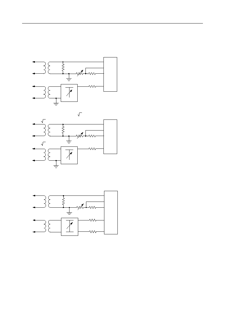
Transmit and Receive Level Adjustment (MSM6996H/V, MSM6997H/V)
4WS
600 W
AIN+
AOUT
a. Transformer of turns ratio 1 : 1
1 : 1
600 W
20 kW
R1
AG
4WR
600 W
1 : 1
600 W Attenuator
600 W
1
2
3
5
AIN≠
GSX
4WS
600 W
AIN+
AOUT
300 W
20 kW
R1
AG
4WR
600 W
300 W Attenuator
300 W
1
2
3
5
AIN≠
GSX
b. Transformer of turns ratio 1 : 2
2 : 1
2 : 1
4WS
600 W
AIN+
AOUT+
1 : 1
600 W
20 kW
R1
AG
4WR
600 W
1 : 1
600 W Attenuator
300 W
1
2
3
5
AIN≠
GSX
300 W 6
AOUT≠
Transmit and Receive Level Adjustment (MSM6998, MSM6999)
When R1 is open and the attenuator is set at
0 dB,
4 WS maximum input level = +7.17 + L
T
(dBm)
4 WR maximum output level = +1.15 ≠ L
T
(dBm)
L
T
: Transformer loss
When R1 is open and the attenuator is set at
0 dB,
4 WS maximum input level = +10.18 + L
T
(dBm)
4 WR maximum output level = +4.16 ≠ L
T
(dBm)
L
T
: Transformer loss
When R1 is open and the attenuator is set at
0 dB,
4 WS maximum input level = +7.17 + L
T
(dBm)
4 WR maximum output level = +7.17 ≠ L
T
(dBm)
L
T
: Transformer loss

° Semiconductor
MSM6996H/6996V/6997H/6997V/6998/6999
18/21
RECOMMENDATIONS FOR ACTUAL DESIGN
∑ To assure proper electrical characteristics, use bypass capacitors with excellent high frequency
characteristics for the power supply and keep them as close as possible to the device pins.
∑ Connect the AG pin and the DG pin each other as close as possible.
Connected to the system ground with low impedance.
∑ Mount the device directly on the board when mounted on printed circuit board.
Do not use IC sockets.
If an IC socket is unavoidable, use the short lead type socket.
∑ When mounted on a frame, use electro-magnetic shielding, if any electro-magnetic wave source
such as power supply transformers surround the device.
∑ Keep the voltage on the V
DD
pin not lower than ≠0.3 V and the voltage on the V
SS
pin more than
+0.3 V even instantaneously to avoid latch-up phenomenon when turning the power on.
∑ Use a low noise (particularly, low level type of high frequency spike noise or pulse noise) power
supply to avoid erroneous operation and the degradation of the characteristics of these devices.
° Semiconductor
MSM6996H/6996V/6997H/6997V/6998/6999
19/21
(Unit : mm)
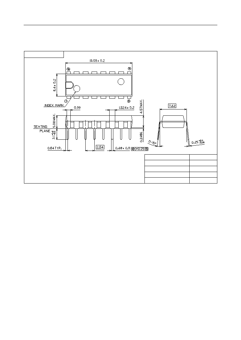
PACKAGE DIMENSIONS
DIP16-P-300-2.54
Package material
Lead frame material
Pin treatment
Solder plate thickness
Package weight (g)
Epoxy resin
42 alloy
Solder plating
5 mm or more
0.99 TYP.
° Semiconductor
MSM6996H/6996V/6997H/6997V/6998/6999
20/21
(Unit : mm)
DIP16-G-300-2.54
16
7.50MAX
2.54
0.80TYP
4.10
±
0.40
5.10MAX
2.54MIN
0.51MIN
1
9
8
0.50
±
0.10
0.25
M
1.50
±
0.10
1.00
±
0.10
20.00MAX
7.62
+0.15
0.25-0.05
0~15
∞
SEATING PLANE
° Semiconductor
MSM6996H/6996V/6997H/6997V/6998/6999
21/21
(Unit : mm)
Notes for Mounting the Surface Mount Type Package
The SOP, QFP, TSOP, SOJ, QFJ (PLCC), SHP and BGA are surface mount type packages, which
are very susceptible to heat in reflow mounting and humidity absorbed in storage.
Therefore, before you perform reflow mounting, contact Oki's responsible sales person for the
product name, package name, pin number, package code and desired mounting conditions
(reflow method, temperature and times).
SOP24-P-430-1.27-K
Package material
Lead frame material
Pin treatment
Solder plate thickness
Package weight (g)
Epoxy resin
42 alloy
Solder plating
5 mm or more
0.58 TYP.
Mirror finish