
° Semiconductor
MSM7533H/7533V/7534
1/18
° Semiconductor
MSM7533H/7533V/7534
2ch Single Rail CODEC
GENERAL DESCRIPTION
The MSM7533 and MSM7534 are two-channel CODEC CMOS ICs for voice signals ranging from
300 to 3400 Hz. These devices contain filters for A/D and D/A conversion.
Designed especially for a single-power supply and low-power applications, these devices
contain two-channel AD/DA converters in a single chip and achieve a reduced footprint and a
reduced number of external components.
The MSM7533 and MSM7534 are best suited for an analog interface to an echo canceller DSP used
in digital telephone terminals, digital PABXs, and hands free terminals.
FEATURES
∑ Single power supply: +5 V
∑ Power consumption
Operating mode:
35 mW Typ.
74 mW Max.
V
DD
= 5 V
Power save mode:
7 mW Typ.
16 mW Max.
V
DD
= 5 V
Power down mode:
0.05 mW Typ.
0.3 mW Max.
V
DD
= 5 V
∑ ITU-T Companding law
MSM7533H:
m-law
MSM7534:
A-law
MSM7533V:
m/A-law pin selectable
∑ Built-in PLL eliminates a master clock
∑ The PCM interface can be switched between 2 channel serial/parallel
∑ Transmission clock: 64/128/256/512/1024/2048 kHz
96/192/384/768/1536/1544/200 kHz
(During 2 channel serial mode, the 64 and 96 kHz clocks are disabled)
∑ Adjustable transmit gain
∑ Built-in reference voltage supply
∑ Analog output can directly drive a 600 W line transformer
∑ Package options:
20-pin plastic skinny DIP (DIP20-P-300-2.54-S1) (Product name : MSM7533HRS)
(Product name : MSM7533VRS)
(Product name : MSM7534RS)
24-pin plastic SOP (SOP24-P-430-1.27-K)
(Product name : MSM7533HGS-K)
(Product name : MSM7533VGS-K)
(Product name : MSM7534GS-K)
E2U0020-28-81
This version: Aug. 1998
Previous version: Nov. 1996
° Semiconductor
MSM7533H/7533V/7534
2/18
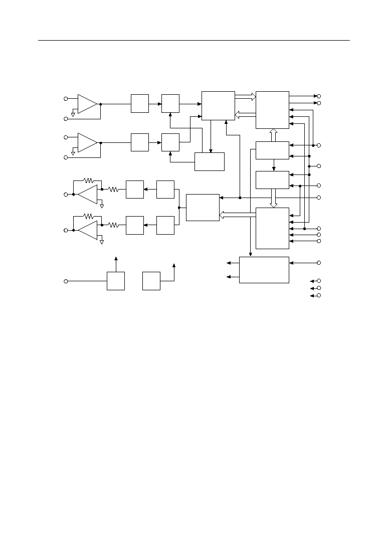
BLOCK DIAGRAM
AIN1
GSX1
AIN2
GSX2
AOUT1
AOUT2
SGC
XSYNC
DOUT1
DOUT2
BCLK
RSYNC
(ALAW)
CHPS
DIN1
DIN2
PDN
V
DD
AG
DG
+
≠
RC
LPF
8th
BPF
RC
LPF
8th
BPF
5th
LPF
S&H
5th
LPF
S&H
SG
GEN
VR
GEN
AD
CONV.
TCONT
AUTO
ZERO
DA
CONV.
PLL
RTIM
RCONT
PWD
Logic
+
≠
+
≠
+
≠
° Semiconductor
MSM7533H/7533V/7534
3/18
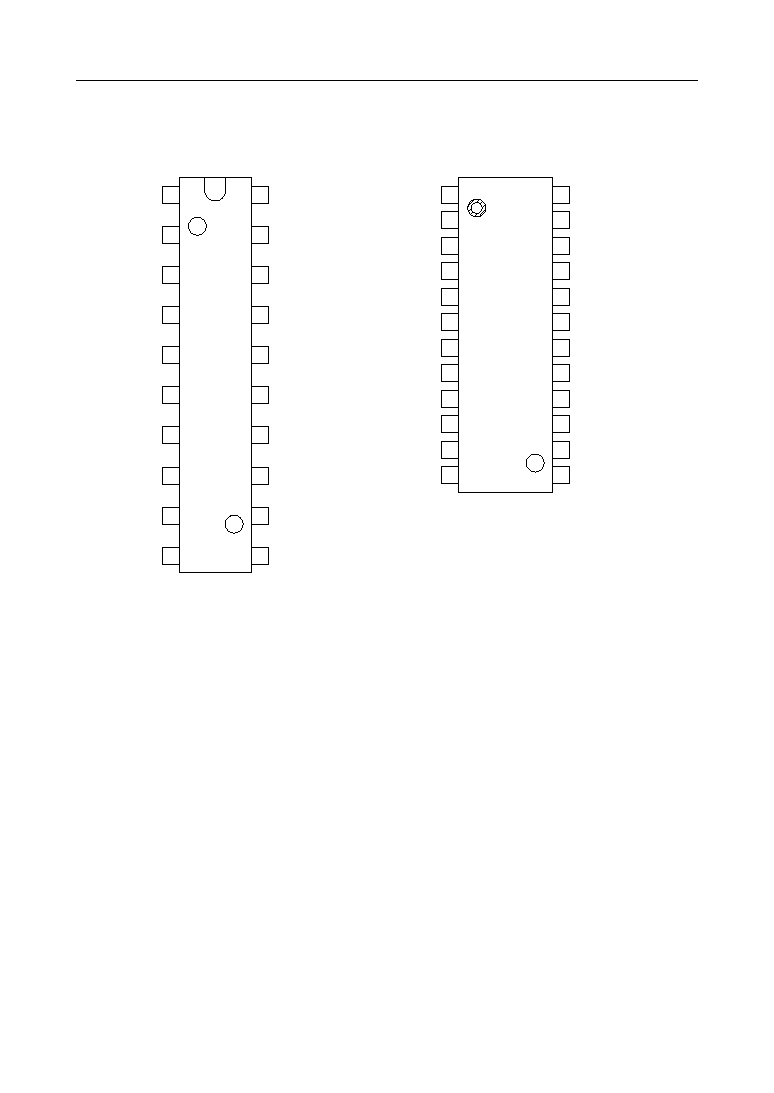
PIN CONFIGURATION (TOP VIEW)
1
2
3
4
5
6
7
8
9
10
11
12
13
14
15
16
17
18
19
20
SGC
AOUT2
AOUT1
PDN
CHPS
VDD
DG
RSYNC
AIN2
GSX2
GSX1
AIN1
(ALAW) *
BCLK
XSYNC
DIN2
DIN1
DOUT2
DOUT1
1
2
3
4
5
6
7
8
9
10
11
12
13
14
15
16
17
18
19
20
21
22
23
24
SGC
AOUT2
NC
PDN
CHPS
V
DD
DG
RSYNC
AIN2
GSX2
GSX1
AIN1
(ALAW) *
BCLK
XSYNC
NC : No connect pin
DIN2
DIN1
DOUT2
DOUT1
AG
AOUT1
NC
AG
NC
NC
20-Pin Plastic Skinny DIP
24-Pin Plastic SOP
* The ALAW pin is only applied to the MSM7533VRS/MSM7533VGS-K.
° Semiconductor
MSM7533H/7533V/7534
4/18
PIN AND FUNCTIONAL DESCRIPTIONS
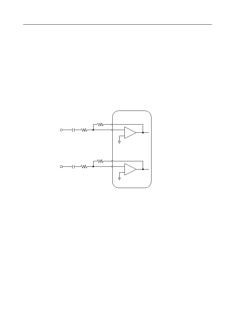
AIN1, AIN2, GSX1, GSX2
AIN1 and AIN2 are the transmit analog inputs for channels 1 and 2.
GSX1 and GSX2 are the transmit level adjustments for channels 1 and 2.
AIN1 and AIN2 are inverting inputs for the op-amp; GSX1 and GSX2 are connected to the output
of the op-amp and are used to adjust the level, as shown below.
When not using AIN1 and AIN2, connect AIN1 to GSX1 and AIN2 to GSX2. During power saving
and power down mode, the GSX1 and GSX2 outputs are at AG voltage.
AOUT1, AOUT2
AOUT1 is the receive analog output for channel 1 and AOUT2 is used for channel 2.
The output signal has an amplitude of 3.4 V
PP
above and below the signal ground voltage (SG).
When the digital signal of +3 dBmO is input to DIN1 and DIN2, it can drive a load of 600 W or
more.
During power saving or power down mode, these outputs are at the voltage level of SG with a
high impedance.
CH1
Analog Input
+
≠
CH2
Analog Input
AIN1
C1
R1
R2
GSX1
AIN2
C2
R3
R4
GSX2
CH1 Gain
Gain = R2/R1 £ 10
R1: Variable
R2 > 20 kW
C1 > 1/(2 • 3.14 • 30 • R1)
+
≠
CH2 Gain
Gain = R4/R3 £ 10
R3: Variable
R4 > 20 kW
C2 > 1/(2 • 3.14 • 30 • R3)

° Semiconductor
MSM7533H/7533V/7534
5/18
V
DD
Power supply for +5 V.
A power supply for an analog circuit of the system which the device is applied should be used.
A bypass capacitor of 0.1 mF to 1 mF with excellent high frequency characteristics and a capacitor
of 10 mF to 20 mF should be connected between this pin and the AG pin if needed.
DIN1
DIN1 is the PCM signal input for channel 1, when the parallel mode is selected.
A serial PCM signal input to this pin is converted to an analog signal in synchronization with the
RSYNC signal and BCLK signal.
The analog signal is output from the AOUT1 pin.
The data rate of the PCM signal is equal to the frequency of BCLK signal.
The PCM signal is shifted at a falling edge of the BCLK signal and latched into the internal register
when shifted by eight bits.
The start of the PCM data (MSD) is identified at the rising edge of RSYNC.
When the serial mode is selected, this pin is not used and should be connected to GND (0 V).
DIN2
DIN2 is the PCM signal input for channel 2, when the parallel mode is selected.
A serial PCM signal input to this pin is converted to an analog signal in synchronization with the
RSYNC signal and BCLK signal.
The analog signal is output from the AOUT2 pin.
The data rate of the PCM signal is equal to the frequency of BCLK signal.
The PCM signal is shifted at a falling edge of the BCLK signal and latched into the internal register
when shifted by eight bits.
The start of the PCM data (MSD) is identified at the rising edge of RSYNC.
When the serial mode is selected, this pin is used for the 2ch multiplexed PCM signal input.
BCLK
Shift clock signal input for the DIN1, DIN2, DOUT1, and DOUT2 signals.
The frequency, equal to the data rate, is 64, 96, 128, 192, 256, 384, 512, 768, 1024, 1536, 1544, 2048,
or 200 kHz. Setting this signal to logic "1" or "0" drives both transmit and receive circuits to the
power saving state.