
° Semiconductor
MSM7543/7544
1/19
° Semiconductor
MSM7543/7544
Single Rail CODEC
GENERAL DESCRIPTION
The MSM7543 and MSM7544 are single-channel CODEC CMOS ICs for voice signals ranging
from 300 to 3400 Hz. These devices contain filters for A/D and D/A conversion.
Designed especially for a single-power supply and low-power applications, these devices are
optimized for telephone terminals in digital wireless systems, ISDN terminals, and digital PBXs.
The MSM7543 and MSM7544 use newly-designed operational amplifiers to keep small current
deviations caused by power voltage fluctuations.
The devices use the same transmission clocks as those used in the MSM7508B and MSM7509B.
The analog output signal, which is of a differential type and can drive a 600 W load, can directly
drive a handset receiver.
FEATURES
∑ Single power supply: +5 V
±
5%
∑ Low power consumption
Operating mode:
20 mW Typ.
31.5 mW Max.
V
DD
= 5 V
Power save mode:
4.5 mW Typ.
8 mW Max.
V
DD
= 5 V
Power down mode:
1.5 mW Typ.
3 mW Max.
V
DD
= 5 V
∑ ITU-T Companding law
MSM7543:
m-law
MSM7544:
A-law
∑ The transmission characteristics of the devices comply with ITU-T G.714
∑ Built-in PLL eliminates a master clock
∑ Serial data rate: 64/128/256/512/1024/2048 kHz
96/192/384/768/1536/1544 kHz
∑ Adjustable transmit gain
∑ Adjustable receive gain
∑ Built-in reference voltage supply
∑ Built-in analog loop back test mode
∑ Differential type analog output. Directly drives a 600 W line transformer
∑ Package options:
20-pin plastic skinny DIP (DIP20-P-300-2.54-S1) (Product name : MSM7543RS)
(Product name : MSM7544RS)
24-pin plastic SOP (SOP24-P-430-1.27-K)
(Product name : MSM7543GS-K)
(Product name : MSM7544GS-K)
26-pin plastic TSOP (TSOPII26/20-P-300-1.27-K) (Product name : MSM7543TS-K)
(Product name : MSM7544TS-K)
E2U0015-28-81
This version: Aug. 1998
Previous version: Nov. 1996
° Semiconductor
MSM7543/7544
2/19
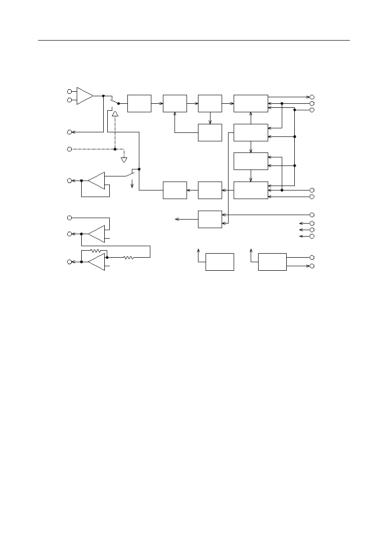
BLOCK DIAGRAM
RC
LPF
BPF
(8th)
AD
Conv.
Transmit
Controller
Auto
Zero
LPF
(5th)
DA
Conv.
PWD
Logic
PLL
R≠TIM
Receive
Controller
PCMOUT
XSYNC
BCLOCK
RSYNC
PCMIN
PDN
V
DD
AG
DG
Signal
Ground
SGC
SG
SG
Voltage
Ref.
Power
Down
+
≠
AIN+
AIN≠
GSX
TMC
≠
+
VFRO
SG
≠
+
AOUT+
SG
≠
+
AOUT≠
SG
PWI
° Semiconductor
MSM7543/7544
3/19
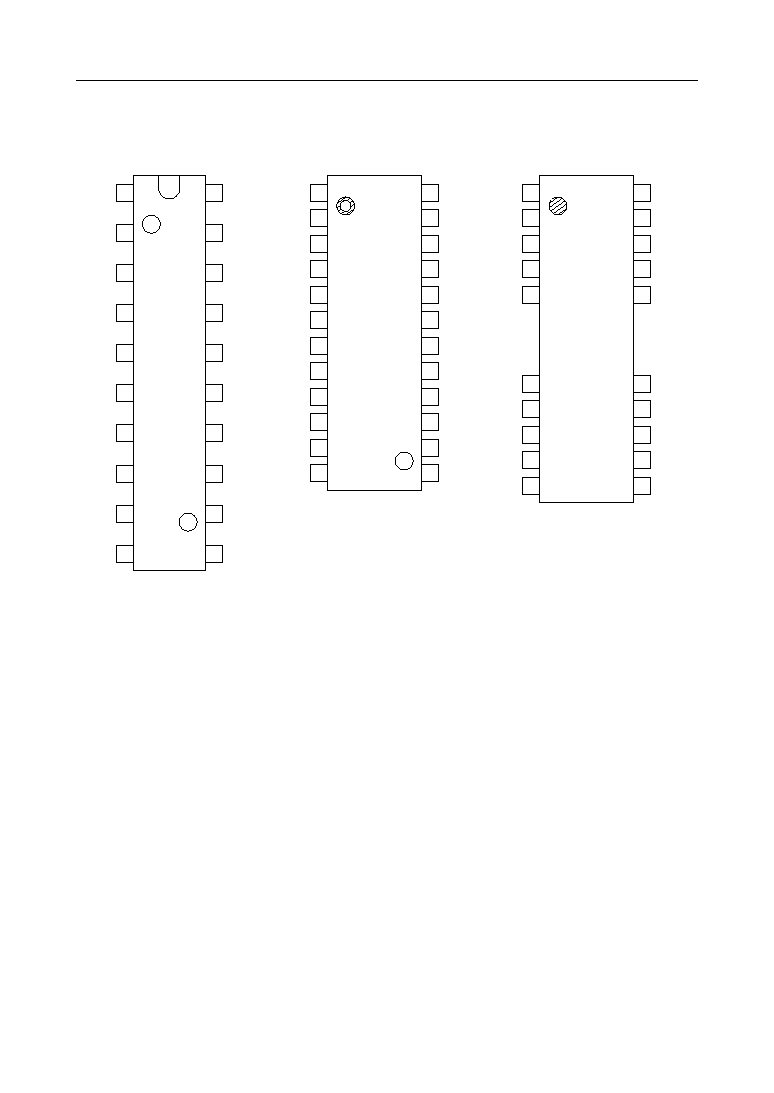
PIN CONFIGURATION (TOP VIEW)
NC : No connect pin
NC : No connect pin
NC : No connect pin
1
2
3
4
5
6
7
8
9
10
11
12
13
14
15
16
17
18
19
20
SG
AOUT+
AOUT≠
PWI
VFRO
V
DD
DG
PDN
SGC
AIN+
AIN≠
GSX
TMC
AG
BCLOCK
RSYNC
PCMIN
XSYNC
PCMOUT
1
2
3
4
5
6
7
8
9
10
11
12
13
14
15
16
17
18
19
20
21
22
23
24
SG
AOUT+
AOUT≠
PWI
VFRO
V
DD
DG
PDN
SGC
AIN+
AIN≠
GSX
TMC
AG
BCLOCK
RSYNC
PCMIN
XSYNC
PCMOUT
1
2
3
4
5
9
10
11
12
13
14
15
16
17
18
22
23
24
25
26
SG
AOUT+
AOUT≠
PWI
VFRO
V
DD
DG
PDN
SGC
AIN+
AIN≠
GSX
AG
BCLOCK
RSYNC
PCMIN
XSYNC
PCMOUT
TMC
NC
NC
NC
NC
NC
NC
NC
24-Pin Plastic SOP
20-Pin Plastic Skinny DIP
26-Pin Plastic TSOP
° Semiconductor
MSM7543/7544
4/19
PIN AND FUNCTIONAL DESCRIPTIONS
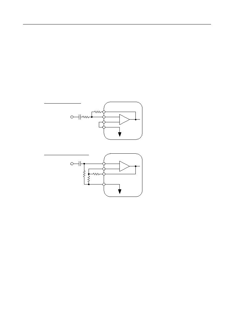
AIN+, AIN≠, GSX
Transmit analog input and transmit level adjustment.
AIN+ is a non-inverting input to the op-amp; AIN≠ is an inverting input to the op-amp; GSX is
connected to the output of the op-amp and is used to adjust the level, as shown below.
When not using AIN≠ and AIN+, connect AIN≠ to GSX and AIN+ to SG. During power saving
and power down modes, the GSX output is at AG voltage.
AG
Analog signal ground.
VFRO
Receive filter output.
The output signal has an amplitude of 2.4 V
PP
above and below the signal ground voltage (SG)
when the digital signal of +3 dBmO is input to PCMIN and can drive a load of 20 kW or more.
For driving a load of 20 kW or less, connect a resistor of 20 kW or more between the pins VFRO
and PWI.
When adding the frequency characteristics to the receive signal, refer to the application example.
During power saving or power down mode, the output of VFRO is at the voltage level of AG.
≠
+
AIN≠
AIN+
C1
Analog input
1) Inverting input type
R1 : variable
R2 > 20 kW
C1 > 1/(2 • 3.14 • 30 • R1)
Gain = R2/R1 £ 10
R2
GSX
SG
+
≠
AIN+
AIN≠
2) Non inverting input type
R3 > 20 kW
R4 > 20 kW
R5 > 50 kW
C2 > 1/ (2 • 3.14 • 30 • R5)
Gain = 1 + R4 / R3 £ 10
R4
GSX
SG
C2
Analog input
R3
R5
R1
° Semiconductor
MSM7543/7544
5/19
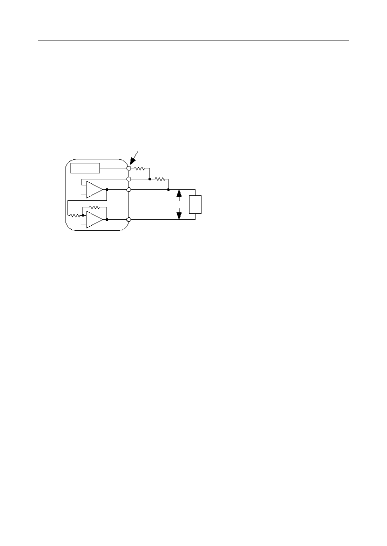
PWI, AOUT+, AOUT≠
PWI is connected to the inverting input of the receive driver. The receive driver output is
connected to the AOUT≠ pin. Therefour, the receive level can be adjusted with the pins VFRO,
PWI, and AOUT≠. When the PWI pin is not used, connect the PWI pin to the AOUT≠ pin, and
leave open the pins AOUT≠ and AOUT+. The output of AOUT+ is inverted with respect to the
output of AOUT≠. Since the signal from which provides differential drive of an impedance of 1.2
kW, these outputs can directly be connected to a receiver of handset using a piezoelectric
earphone. Refer to the application example.
R6 > 20 kW
ZL 1.2 kW
Gain = VO/VI = 2 • R7/R6 £ 2
R6
R7
≠
+
SG
≠
+
SG
VFRO
PWI
AOUT≠
AOUT+
Receive Filter
ZL
VO
VI
During power saving and power down modes, the outputs of AOUT+ and AOUT≠ are in a high
impedance state .
The electrical driving capability of the AOUT≠ pin and AOUT+ pin is
±
1.3 V maximum. The
output load resistor has a minimum value of 0.6 kW.
If an output amplitude less than
±
1.3 V is allowed, these outputs can drive a load resistance less
than that described above.
For more details, refer to SINGLE POWER SUPPLY PCM CODEC APPLICATION NOTE.
V
DD
Power supply pin for +5 V.
PCMIN
PCM signal input.
A serial PCM signal input to this pin is converted to an analog signal in synchronization with the
RSYNC signal and BCLOCK signal.
The data rate of the PCM signal is equal to the frequency of the BCLOCK signal.
The PCM signal is shifted at a falling edge of the BCLOCK signal and latched into the internal
register when shifted by eight bits.
The start of the PCM data (MSD) is identified at the rising edge of RSYNC.
BCLOCK
Shift clock signal input for the PCMIN and PCMOUT signal.
The frequency, equal to the data rate, is 64, 96, 128, 192, 256, 384, 512, 768, 1024, 1536, 1544, 2048,
or 200 kHz. Setting this signal to logic "1" or "0" drives both transmit and receive circuits to the
power saving state.

° Semiconductor
MSM7543/7544
6/19
RSYNC
Receive synchronizing signal input.
Eight required bits are selected from serial PCM signals on the PCMIN pin by the receive
synchronizing signal.
Signals in the receive section are synchronized by this synchronizing signal. This signal must be
synchronized in phase with the BCLOCK. The frequency should be 8 kHz
±
50 ppm to guarantee
the AC characteristics which are mainly the frequency characteristics of the receive section.
However, if the frequency characteristic of an applied system is not specified exactly, this device
can operate in the range of 8 kHz
±
2 kHz, but the electrical characteristics in this specification are
not guaranteed.
XSYNC
Transmit synchronizing signal input.
The PCM output signal from the PCMOUT pin is output in synchronization with this transmit
synchronizing signal. This synchronizing signal triggers the PLL and synchronizes all timing
signals of the transmit section.
This synchronizing signal must be synchronized in phase with BCLOCK.
The frequency should be 8 kHz
±
50 ppm to guarantee the AC characteristics which are mainly
the frequency characteristics of the transmit section.
However, if the frequency characteristic of an applied system is not specified exactly, this device
can operate in the range of 8 kHz
±
2 kHz, but the electrical characteristics in this specification are
not guaranteed.
Setting this signal to logic "1" or "0" drives both transmit and receive circuits to the power saving
state.
TMC
Control signal input for mode selection.
This pin select the normal operating mode or the analog loop-back mode.
In the analog loop-back mode, the receive filter output is connected to the transmit filter input
and the digital signal input to the PCMIN pin is converted from a digital to an analog signal (D/
A conversion). Next, the analog signal is converted to a digital signal (A/D conversion) through
the receive filter and transmit filter. The result is output to the PCMOUT pin.
When in the analog loop-back mode, the VFRO pin outputs the SG level. (signal ground)
TMC Input
< 0.8 V
> 2.2 V
Mode
Normal operation
Analog loop-back
° Semiconductor
MSM7543/7544
7/19
DG
Ground for the digital signal circuits.
This ground is separate from the analog signal ground. The DG pin must be connected to the AG
pin on the printed circuit board to make a common analog ground.
PDN
Power down control signal.
A logic "0" level drives both transmit and receive circuits to a power down state.
PCMOUT
PCM signal output.
The PCM output signal is output from MSD in a sequential order, synchronizing with the rising
edge of the BCLOCK signal.
MSD may be output at the rising edge of the XSYNC signal, based on the timing between
BCLOCK and XSYNC.
This pin is in a high impedance state except during 8-bit PCM output. It is also in a high
impedance state during power saving or power down modes.
A pull-up resistor must be connected to this pin because its output is configured as an open drain.
This device is compatible with the ITU-T recommendation on coding law and output coding
format.
The MSM7544(A-law) outputs the character signal, inverting the even bits.
Input/Output Level
+Full scale
+0
≠0
≠Full scale
PCMIN/PCMOUT
MSM7543 (
m-law)
MSD
1
0
0
0
0
0
0
0
1
1
1
1
1
1
1
1
0
1
1
1
1
1
1
1
0
0
0
0
0
0
0
0
MSM7544 (A-law)
MSD
1
0
1
0
1
0
1
0
1
1
0
1
0
1
0
1
0
1
0
1
0
1
0
1
0
0
1
0
1
0
1
0
SG
Signal ground voltage output.
The output voltage is 1/2 of the power supply voltage.
The output drive current capability is
±
300 mA.
This pin provides the SG level for CODEC peripherals.
This output voltage level is undefined during power saving or power down modes.
SGC
Used to generate the signal ground voltage level by connecting a bypass capacitor.
Connect a 0.1 mF capacitor with excellent high frequency characteristics between the AG pin and
the SGC pin.
° Semiconductor
MSM7543/7544
8/19
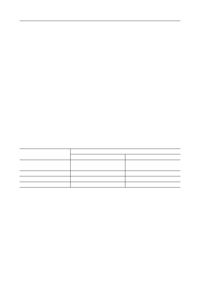
ABSOLUTE MAXIMUM RATINGS
Parameter
Power Supply Voltage
Analog Input Voltage
Digital Input Voltage
Storage Temperature
Symbol
V
DD
V
AIN
V
DIN
T
STG
Condition
--
--
--
--
Rating
0 to 7
≠0.3 to V
DD
+ 0.3
≠0.3 to V
DD
+ 0.3
≠55 to +150
Unit
V
V
V
∞C
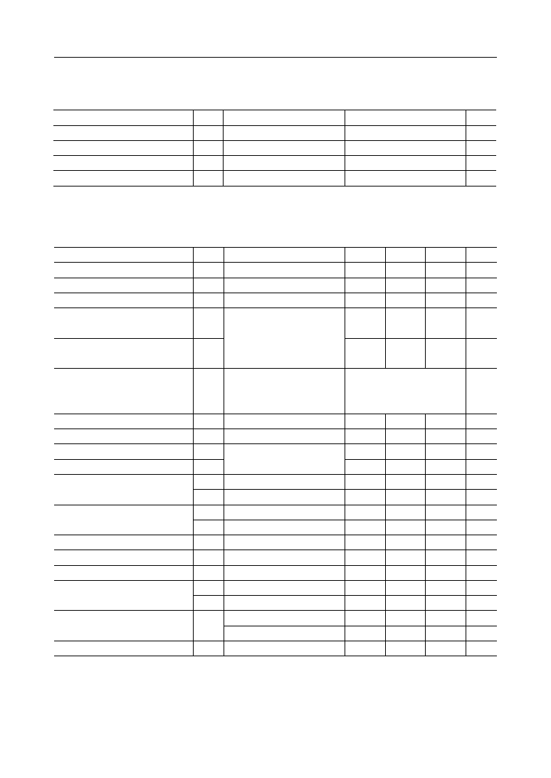
RECOMMENDED OPERATING CONDITIONS
Parameter
Symbol
Power Supply Voltage
Analog Input Voltage
Digital Input High Voltage
Digital Input Low Voltage
Clock Frequency
Sync Pulse Frequency
Clock Duty Ratio
Digital Input Rise Time
Digital Input Fall Time
Transmit Sync Pulse Setting Time
Receive Sync Pulse Setting Time
Sync Pulse Width
PCMIN Set-up Time
PCMIN Hold Time
Digital Output Load
Analog Input Allowable DC Offset
Allowable Jitter Width
V
DD
V
AIN
V
IH
V
IL
F
C
F
S
D
C
t
Ir
t
If
t
XS
t
WS
t
DS
t
DH
R
DL
V
off
t
SX
t
RS
t
SR
--
Condition
Connect AIN≠ and GSX
XSYNC, RSYNC, BCLOCK,
PCMIN, PDN, TMC
BCLOCK
XSYNC, RSYNC
BCLOCK
XSYNC, RSYNC, BCLOCK,
PCMIN, PDN, TMC
BCLOCK∆XSYNC, See Timing Diagram
XSYNC, RSYNC
--
--
Pull-up resistor
Transmit gain stage, Gain = 10
XSYNC∆BCLOCK, See Timing Diagram
BCLOCK∆RSYNC, See Timing Diagram
RSYNC∆BCLOCK, See Timing Diagram
Transmit gain stage, Gain = 1
XSYNC, RSYNC, BCLOCK
--
Min.
Typ.
Max.
Unit
4.75
--
2.2
0
64, 128, 256, 512, 1024,
2048, 96, 192, 384, 768,
1536, 1544, 200
6.0
40
--
--
100
1 BCLK
100
100
0.5
≠10
100
100
100
≠100
--
--
5.0
--
--
--
8.0
50
--
--
--
--
--
--
--
--
--
--
--
--
--
--
5.25
2.4
V
DD
0.8
10.0
60
50
50
--
100
--
--
--
+10
--
--
--
+100
500
100
V
V
PP
V
V
kHz
%
ns
ns
ns
ms
ns
ns
kW
mV
ns
ns
ns
mV
ns
pF
kHz
C
DL
Voltage must be fixed
Operating Temperature
T
a
--
+25
∞C
≠30
+85
° Semiconductor
MSM7543/7544
9/19
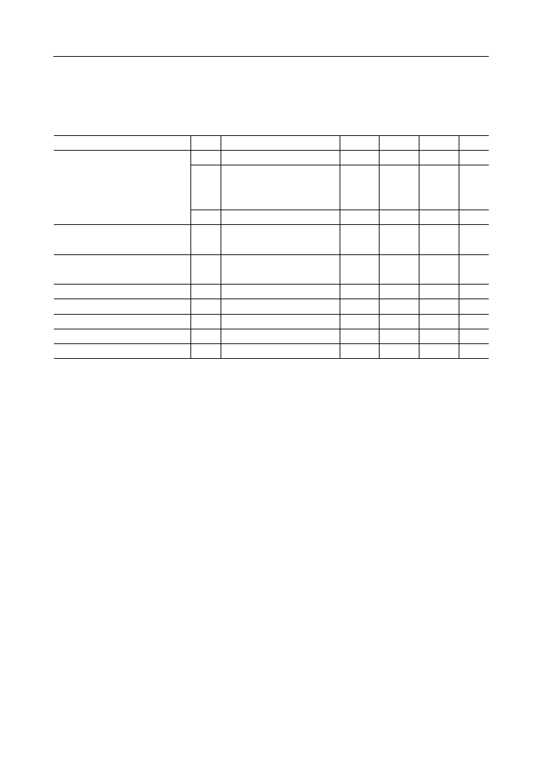
ELECTRICAL CHARACTERISTICS
DC and Digital Interface Characteristics
Parameter
Power Supply Current
Input High Voltage
Input Low Voltage
High Level Input Leakage Current
Low Level Input Leakage Current
Digital Output Low Voltage
Digital Output Leakage Current
Input Capacitance
Symbol
I
DD1
I
DD2
I
DD3
V
IH
V
IL
I
IH
I
IL
V
OL
I
O
Condition
Operating mode, No signal
Power-save mode, PDN = 1,
XSYNC or BCLOCK ∆ OFF
Power-down mode, PDN = 0
--
--
--
--
Pull-up resistance > 500 W
--
Min.
--
--
--
2.2
0.0
--
--
0.0
--
Typ.
4.0
0.9
0.3
--
--
--
--
0.2
--
Max.
6.0
1.5
0.5
V
DD
0.8
2.0
0.5
0.4
10
Unit
mA
mA
mA
V
V
mA
mA
V
mA
C
IN
--
--
5
--
pF
(V
DD
= +5 V ±5%, Ta = ≠30∞C to +85∞C)
° Semiconductor
MSM7543/7544
10/19
Transmit Analog Interface Characteristics
Input Resistance
Output Load Resistance
Output Load Capacitance
Output Amplitude
Offset Voltage
R
INX
R
LGX
C
LGX
V
OGX
V
OSGX
AIN+, AIN≠
Gain = 1
10
20
--
≠1.2
≠20
--
--
--
--
--
--
--
100
+1.2
+20
MW
kW
pF
V
mV
GSX with respect to SG
Parameter
Symbol
Condition
Min.
Typ.
Max.
Unit
(V
DD
= +5 V ±5%, Ta = ≠30∞C to +85∞C)
Receive Analog Interface Characteristics
Input Resistance
Output Load Resistance
Output Load Capacitance
R
INPW
R
LVF
R
LAO
C
LVF
C
LAO
PWI
10
20
0.6
--
--
--
--
--
--
--
--
--
--
100
50
MW
kW
kW
pF
pF
VFRO with respect to SG
Output Amplitude
Offset Voltage
V
OVF
V
OAO
V
OSVF
V
OSAO
≠1.2
≠1.3
≠100
≠100
--
--
--
--
+1.2
+1.3
+100
+100
V
V
mV
mV
VFRO, R
L
= 20 kW with
respect to SG
AOUT+, AOUT≠ (each) with
respect to SG
VFRO
AOUT+, AOUT≠
AOUT+, AOUT≠, R
L
= 1.2 kW
with respect to SG
VFRO with respect to SG
AOUT+, AOUT≠, Gain = 1 with
respect to SG
Parameter
Symbol
Condition
Min.
Typ.
Max.
Unit
(V
DD
= +5 V ±5%, Ta = ≠30∞C to +85∞C)
° Semiconductor
MSM7543/7544
11/19
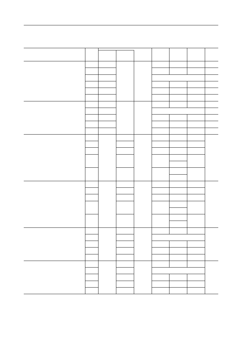
AC Characteristics
Loss T1
60
20
26
--
dB
Loss T2
300
≠0.20
+0.07
+0.20
dB
Loss T3
1020
Reference
dB
0
Loss T4
2020
≠0.15
≠0.04
+0.20
dB
Loss T5
3000
≠0.15
+0.06
+0.20
dB
Loss T6
3400
0
0.4
0.80
dB
Loss R1
300
≠0.15
≠0.03
+0.20
dB
Loss R2
1020
Reference
dB
Loss R3
2020
≠0.15
≠0.02
+0.20
dB
0
Loss R4
3000
≠0.15
+0.15
+0.20
dB
Loss R5
3400
0.0
0.56
0.80
dB
SD T1
35
43
--
3
SD T2
35
41
--
0
SD T3
35
38
--
≠30
SD T4
1020
29
31.5
--
dB
≠40
*2
31.0
SD T5
*1
24
27
--
≠45
*2
26
SD R1
36
43
--
3
SD R2
36
41
--
0
SD R3
36
40
--
≠30
SD R4
1020
30
34.5
--
dB
≠40
*2
32
SD R5
*1
25
30
--
≠45
*2
27
GT T1
≠0.2
+0.01
+0.2
GT T2
Reference
GT T3
1020
≠0.2
0
+0.2
dB
≠40
GT T4
≠0.4
≠0.03
+0.4
GT T5
≠1.2
+0.15
+1.2
3
≠10
≠50
≠55
GT R1
≠0.2
≠0.06
+0.2
GT R2
Reference
GT R3
1020
≠0.2
≠0.02
+0.2
dB
GT R4
≠0.4
≠0.02
+0.4
GT R5
≠0.8
≠0.27
+0.8
≠40
3
≠10
≠50
≠55
Transmit Frequency Response
Receive Frequency Response
Transmit Signal to Distortion Ratio
Receive Signal to Distortion Ratio
Transmit Gain Tracking
Receive Gain Tracking
Condition
Parameter
Symbol
Min.
Typ.
Max.
Unit
Level
(dBm0)
Freq.
(Hz)
(V
DD
= +5 V ±5%, Ta = ≠30∞C to +85∞C)
*1 Psophometric filter is used
*2 Upper is specified for the MSM7543, lower for the MSM7544
° Semiconductor
MSM7543/7544
12/19
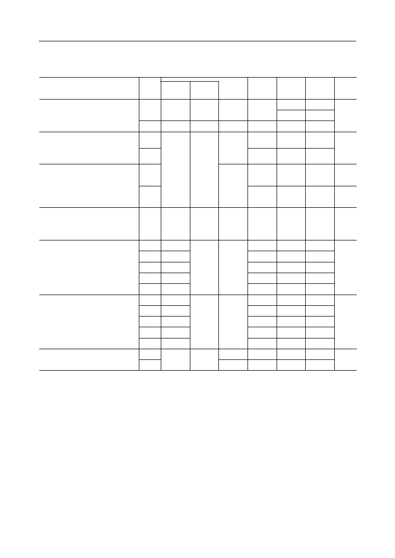
AC Characteristics (Continued)
Absolute Level (Initial Difference)
Nidle T
--
--
≠74.5
≠72.5
dBmOp
Nidle R
--
≠78
AV T
0.580
0.6007
0.622
AV R
0.580
0.6007
0.622
Vrms
1020
Absolute Delay
AV Tt
≠0.2
--
+0.2
0
AV Rt
≠0.2
--
+0.2
Td
1020
--
--
0.60
ms
0
A to A
BCLOCK
= 64 kHz
Transmit Group Delay
tgd T1
--
0.19
0.75
tgd T2
--
0.11
0.35
tgd T3
--
0.02
0.125
0
tgd T4
--
0.05
0.125
ms
*5
0.07
tgd T5
--
0.75
Receive Group Delay
--
0.00
0.75
0.00
--
0.00
0.125
ms
0
--
0.09
0.125
--
0.12
0.75
--
≠75
Idle Channel Noise
--
--
AIN = SG
*1 *3
*1 *2
dB
dB
V
DD
= 5.0 V
Ta = 25∞C
V
DD
=
+5 V ±5%
Ta = ≠30
to 85∞C
Absolute Level
(Deviation of Temperature and Power)
*4
500
600
1000
2600
2800
Crosstalk Attenuation
CR T
75
80
--
CR R
76
1020
dB
0
TRANS ∆ RECV
RECV ∆ TRANS
tgd R1
tgd R2
tgd R3
tgd R4
tgd R5
500
600
1000
2600
2800
*5
70
--
--
0.35
Condition
Parameter
Symbol
Min.
Typ.
Max.
Unit
Level
(dBm0)
Freq.
(Hz)
*4
(V
DD
= +5 V ±5%, Ta = ≠30∞C to +85∞C)
≠70
≠69
*1 Psophometric filter is used
*2 Upper is specified for the MSM7543, lower for the MSM7544
*3 Input "0" code to PCMIN
*4 AVR is defined at VFRO output
*5 Minimum value of the group delay distortion
° Semiconductor
MSM7543/7544
13/19
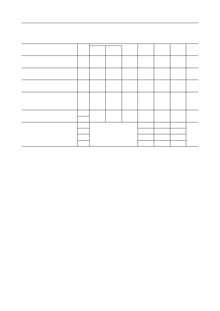
AC Characteristics (Continued)
DIS
4.6 kHz to
30
32
--
dB
Digital Output Delay Time
t
SD
50
--
200
t
XD1
50
--
200
t
XD2
50
--
200
t
XD3
50
--
200
ns
Discrimination
0
0 to
4000 Hz
C
L
= 100 pF + 1 LSTTL
S
300 to
--
≠37.5
≠35
dBmO
Out-of-band Spurious
0
4.6 kHz to
IMD
fa = 470
--
≠52
≠35
dBmO
Intermodulation Distortion
≠4
2fa ≠ fb
--
1020
≠1.0
--
+1.0
dB
D-to-D Mode Gain
0
TMC = 1
PCMIN to
PCMOUT
PSR T
0 to
--
30
--
dB
Power Supply Noise Rejection Ratio
50 mV
PP
*6
PSR R
72 kHz
3400
fb = 320
50 kHz
100 kHz
Condition
Parameter
Symbol
Min.
Typ.
Max.
Unit
Level
(dBm0)
Freq.
(Hz)
(V
DD
= +5 V ±5%, Ta = ≠30∞C to +85∞C)
*6 The measurement under idle channel noise
° Semiconductor
MSM7543/7544
14/19
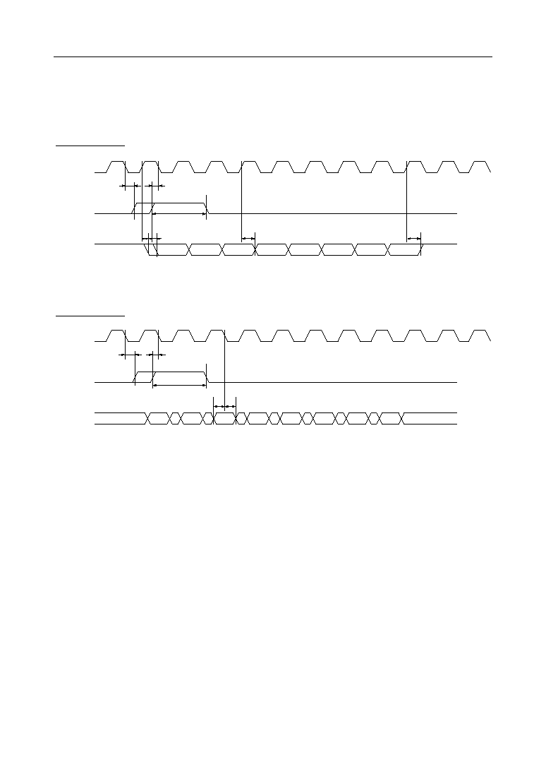
TIMING DIAGRAM
PCM Data Input/Output Timing
BCLOCK
1
2
3
4
5
6
7
8
9
10
XSYNC
PCMOUT
D2
D3
D4
D5
D6
D7
D8
MSD
t
XS
t
SX
t
WS
t
SD
t
XD1
t
XD2
t
XD3
BCLOCK
1
2
3
4
5
6
7
8
9
10
RSYNC
PCMIN
D2
D3
D4
D5
D6
D7
MSD
t
RS
t
SR
t
WS
t
DS
t
DH
D8
Transmit Timing
Receive Timing
,
11
When t
XS
£ 1/2 ∑ Fc, the Delay of the MSD bit is defined as t
XD1
.
When t
SX
£ 1/2 ∑ Fc, the Delay of the MSD bit is defined as t
SD
.
11
,
° Semiconductor
MSM7543/7544
15/19
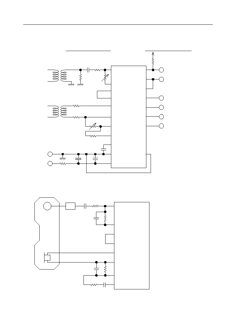
APPLICATION CIRCUIT
1:1
Analog input
600 W
PCMOUT
XSYNC
AIN≠
GSX
AIN+
0.1 mF
PCM signal output
8 kHz SYNC signal input
PCM shift clock input
PCM data input
Power Down control input
Analog interface
Digital interface
0.1 mF
51 kW
1 mF
10 mF
+
MSM7543/7544
SG
RSYNC
BCLOCK
PCMIN
+5 V
PDN
DG
AOUT≠
PWI
VFRO
SGC
AG
V
DD
0 V
+5 V
51 kW
Analog loop-back
control input
TMC
0 to 22 W
300 W
1:1
Analog input
600 W
300 W
AOUT+
FREQUENCY CHARACTERISTICS ADJUSTMENT CIRCUIT
AIN≠
Transmit frequency
characteristic
Adjustment determined with
C1, C2, R1, R2.
Receive frequency
characteristic
Adjustment determined with
C3, C4, R3, R4.
GSX
AIN+
SG
AOUT+
AOUT≠
PWI
VFRO
R2
C2
R4
C4
R1
C1
M
R3
C3
Microphone amp

° Semiconductor
MSM7543/7544
16/19
RECOMMENDATIONS FOR ACTUAL DESIGN
∑ To assure proper electrical characteristics, use bypass capacitors with excellent high frequency
characteristics for the power supply and keep them as close as possible to the device pins.
∑ Connect the AG pin and the DG pin each other as close as possible. Connect to the system
ground with low impedance.
∑ Mount the device directly on the board when mounted on PCBs. Do not use IC sockets. If an
IC socket is unavoidable, use the short lead type socket.
∑ When mounted on a frame, use electro-magnetic shielding, if any electro-magnetic wave
source such as power supply transformers surround the device.
∑ Keep the voltage on the V
DD
pin not lower than ≠0.3 V even instantaneously to avoid latch-
up phenomenon when turning the power on.
∑ Use a low noise (particularly, low level type of high frequency spike noise or pulse noise)
power supply to avoid erroneous operation and the degradation of the characteristics of these
devices.
° Semiconductor
MSM7543/7544
17/19
(Unit : mm)
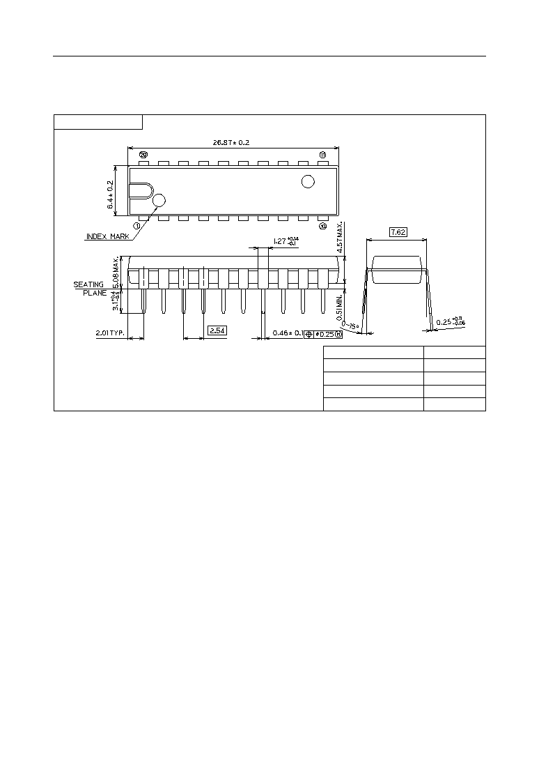
PACKAGE DIMENSIONS
DIP20-P-300-2.54-S1
Package material
Lead frame material
Pin treatment
Solder plate thickness
Package weight (g)
Epoxy resin
42 alloy
Solder plating
5 mm or more
1.49 TYP.
° Semiconductor
MSM7543/7544
18/19
(Unit : mm)
Notes for Mounting the Surface Mount Type Package
The SOP, QFP, TSOP, SOJ, QFJ (PLCC), SHP and BGA are surface mount type packages, which
are very susceptible to heat in reflow mounting and humidity absorbed in storage.
Therefore, before you perform reflow mounting, contact Oki's responsible sales person for the
product name, package name, pin number, package code and desired mounting conditions
(reflow method, temperature and times).
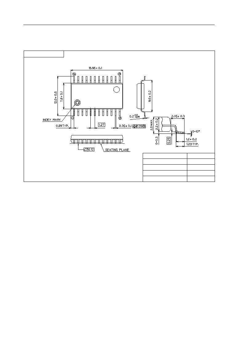
SOP24-P-430-1.27-K
Package material
Lead frame material
Pin treatment
Solder plate thickness
Package weight (g)
Epoxy resin
42 alloy
Solder plating
5 mm or more
0.58 TYP.
Mirror finish
° Semiconductor
MSM7543/7544
19/19
(Unit : mm)
Notes for Mounting the Surface Mount Type Package
The SOP, QFP, TSOP, SOJ, QFJ (PLCC), SHP and BGA are surface mount type packages, which
are very susceptible to heat in reflow mounting and humidity absorbed in storage.
Therefore, before you perform reflow mounting, contact Oki's responsible sales person for the
product name, package name, pin number, package code and desired mounting conditions
(reflow method, temperature and times).
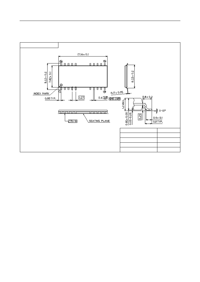
TSOP
II26/20-P-300-1.27-K
Package material
Lead frame material
Pin treatment
Solder plate thickness
Package weight (g)
Epoxy resin
42 alloy
Solder plating
5 mm or more
0.38 TYP.
Mirror finish