 | –≠–ª–µ–∫—Ç—Ä–æ–Ω–Ω—ã–π –∫–æ–º–ø–æ–Ω–µ–Ω—Ç: MSM7557 | –°–∫–∞—á–∞—Ç—å:  PDF PDF  ZIP ZIP |

1/25
MSM7557
° Semiconductor
GENERAL DESCRIPTION
The MSM7557 is a single chip MSK modem with base band voice processor for cordless telephone.
The MSM7557 voice transmit block consists of high pass filter, compressor, pre-emphasis, limiter
and splatter filter.
Voice receive block consists of Band pass filter, De-emphasis and Expander.
FEATURES
∑
∑
∑
∑
∑ Available to transmit modem signal and also transmit base band voice signal through wireless
transmission path (0.3 kHz to 3.4 kHz)
∑
∑
∑
∑
∑ Built-in compandor circuit
∑
∑
∑
∑
∑ Upper limit of voice band (3306 Hz/3400 Hz/3500 Hz) is selectable
∑
∑
∑
∑
∑ Modem bit rate (2400/1200 bps) is selectable
∑
∑
∑
∑
∑ Transmit function and receive function operate separately
∑
∑
∑
∑
∑ Emphasis mode selectable
∑
∑
∑
∑
∑ Built-in bit synchronous detector and frame synchronous detector
∑
∑
∑
∑
∑ Built-in limiter level generator and external limit voltage input
∑
∑
∑
∑
∑ Dynamic range selectable
∑
∑
∑
∑
∑ Built-in crystal oscillator circuit
∑
∑
∑
∑
∑ Wide range power supply voltage (2.7V ~ 5.5V)
∑
∑
∑
∑
∑ Package :
56-pin plastic QFP
(QFP56-P-910-0.65-2K) (Product name : MSM7557GS-2K)
° Semiconductor
MSM7557
Single Chip MSK Modem with Compandor for Cordless Telephone
E2A0046-16-X1
This version: Jan. 1998
Previous version: Nov. 1996
2/25
MSM7557
° Semiconductor
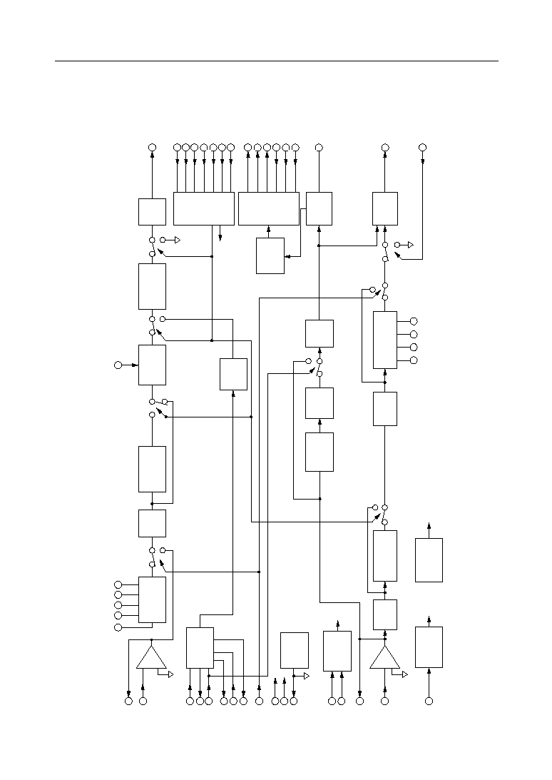
BLOCK DIAGRAM
TVIO
TVI
SD
ST
BR
VR1
VR2
VR3
BYP
VDD
GND
SG
X1
X2
RAIO
RAI
PDN
CMPI
CC1
CC2
CC3N
CC3P
LIM
≠
+
TAO
SEC
DYN
TVE
ME
EMP
RCK1
RCK2
RD
RT
FD
FPS
BIT
FDE
CSH
RVO
RVE
CE1
CE2
CE3N
CE3P
≠
+
Com-
pressor
HPF1
Pre-
Emphasis
Limiter
Splatter
Filter
RC-
LPF
CONT
Flame
Det
Shaper
RC-
LPF
Expander
HPF2
RBPF
De-
Emphasis
Voltage
REF
PDN
OSC
SG
Mix LPF
Mixer
DEM-
BPF
DEMOD
RC-
LPF
MOD
3/25
MSM7557
° Semiconductor
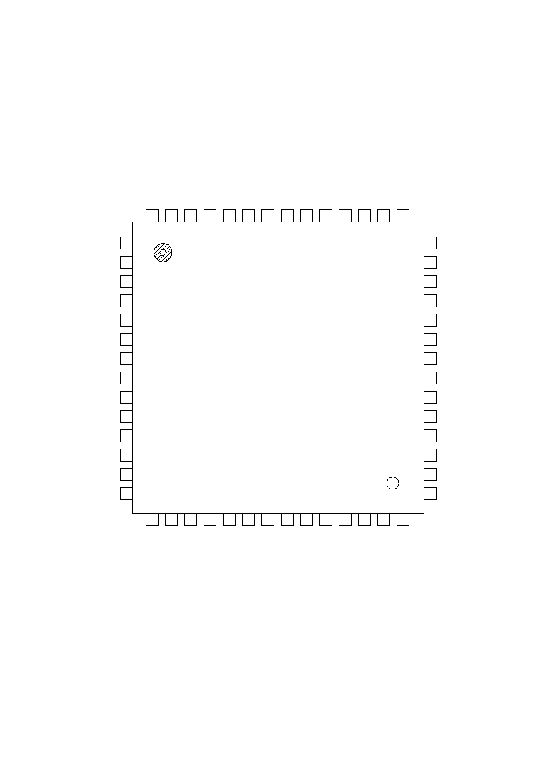
PIN CONFIGURATION (TOP VIEW)
NC
1
ST
2
EMP
3
LIM
4
NC
5
VR1
6
VR2
7
VR3
8
NC
9
TVIO
10
CMPI
11
TVI
12
CC1
13
CC2
14
NC
42
BIT
41
FDE
40
BR
39
BYP
38
RCK2
37
RCK1
36
SEC
35
CSH
34
RAI
33
NC
32
RAIO
31
CE3P
30
NC
29
NC
15
CC3N
16
CC3P
17
DYN
18
SG
19
NC
20
(VDD)
21
GND
22
TAO
23
RVO
24
CE1
25
CE2
26
CE3N
27
NC
28
SD
56
TVE
55
ME
54
X2
53
X1
52
NC
51
PDN
50
VDD
49
RVE
48
RT
47
RD
46
FD
45
FPS
44
NC
43
Notes: The pin 49 should be used for V
DD
.
The pin 21 should be connected to V
DD
or opened.
NC : No connect pin
4/25
MSM7557
° Semiconductor
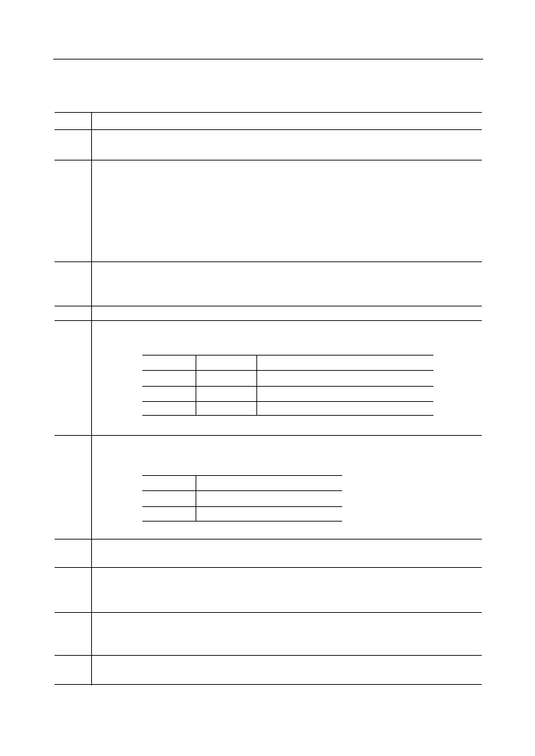
PIN DESCRIPTION
Name
SD
EMP
Pre-emphasis circuit is bypassed to the
path
De-emphasis circuit is bypassed to the
path
Description
t
MS
ME
SD input
ST
Modulator
input data
Transmit side
Receive side
DYN
0
0.50 V
≠9 dBV
Internal clamp level
Limiter level
ST
EMP
LIM
0
1
Pre-emphasis circuit is connected to the
path
De-emphasis circuit is connected to the
path
Transmit data input.
The data on SD pin are took into MSK modulator and the data are available on the positive edge of ST.
In order to synchronize a receive modem, more than 18bits bit-synchronous signal should be
transmitted before data transmission. If S/N ratio of the receive signal is always good, more than
11bits bit-synchronous signal synchronizes the receiver.
Transmit data timing clock output.
When digital "0" is put on ME pin, ST is fixed to digital "1" level.
Emphasis path selection.
Deviation limiter control.
Voice signal maximum Rf modulation level is controlled by connecting external reference voltage to
this pin.
Input impedance of this pin is about 200 kW.
When this pin is left open, internal reference voltage is used as the clamp level.
Internal clamp level is as follows.
This internal clamp level is made by internal reference voltage which is unrelated with V
DD
.
Negative clamp level is made by internal operational amplifier and the voltage is reversed at VSG.
1
1.26 V
≠1 dBV
5/25
MSM7557
° Semiconductor
(Continued)
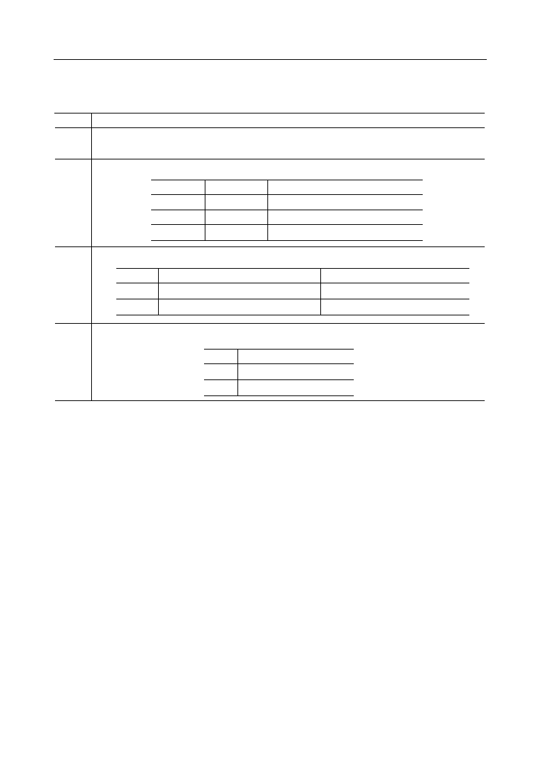
Name
VR1
VR2
VR3
Modulator output level control.
Refer to the following figure.
Description
+
≠
From modulator
+
≠
To transmit filter
VR1
VR2
VR3
R1
R2
R1 40 kW
R2 40 kW
R1 R2
+
≠
C1
R3
R5
C2
R4
C3
TVIO
TVI
SG
VTVI
CMPI
Compressor
R5 60 kW
C1 and C19 are used for DC cut.
Example of fc = 10 kHz and 0 dB gain
R3 = R4 = R5 = 68 kW
C1 = 0.22 mF, C2 = 510 pF, C3 = 110 pF
C19
TVIO
TVI
CC1
CC2
CC3N
CC3P
V
TAO
= 20 • log (R2/R1) ≠ 9 dBV (DYN = "0" )
V
TAO
= 20 • log (R2/R1) ≠ 1 dBV (DYN = "1" )
This level is made from internal voltage reference, so this level doesn't depend on power supply voltage.
Transmit side RC active filter input (TVI) and output (TVIO).
If over 50 kHz frequency element is in the input signal, folding noise is generated from internal SCF
circuit, so second order RC-active filter is needed. (fc = 10 kHz)
When digital "1" is applied to TVE pin, transmit voice signal comes out to TAO.
Capacitor connection pins to remove for DC offset of the compressor.
A 1 mF capacitor between SG pin and each pin should be connected.
Capacitor connection pins for the compressor attack and recovery time.
When DYN is digital "0" level, a 0.22 mF capacitor should be connected between CC3N and CC3P.
And when DYN is digital "1" level, a 0.47 mF capacitor should be connected between them.
6/25
MSM7557
° Semiconductor
(Continued)
Name
Description
ME
TVE
TAO
X : Don't care
RVE
RVO
0
1
Output disable (potential = SG)
Output enable
CMPI
DYN
SG
GND
TAO
RVO
CE1
CE2
CE3N
CE3P
RAIO
RAI
CSH
0
0
0
1
1
X
No signal output (potential = SG)
Voice signal output
MSK modulator output
Compressor circuit input.
A 0.47 mF capacitor should be connected between CMPI and TVIO.
Dynamic range control input.
For an application of which V
DD
is always higher than 4.5 V (Base station), by setting DYN = "1",
modem transmit carrier level, typical input signal level, limiter clamp level and compandor
standard input level are up about 8dB to improve S/N ratio.
For an application of which V
DD
is lower than 4.5 V (Hand-set) DYN shall be digital "0".
To make easier interface with the RF part, one solution is to put digital "0" on DYN pin for both Base
station and Handset.
Built-in analog signal ground. The DC voltage is half of V
DD
.
To make this voltage source impedance lower and to ensure the device performance, it is necessary to
put a bypass capacitor of more than 1mF between SG and V
DD
in close physical proximity to the device.
Ground pin, (0V).
Transmit analog signal output.
According to control data on ME and TVE, TAO is set as follows.
Receive voice signal output.
RVO pin state is defined by RVE control.
Capacitor connection pins to remove DC offset of the expander.
A 1 mF capacitor between SG pin and each pin should be connected.
Capacitor connection pins for the expander attack time and recovery time.
When DYN is digital "0" level, a 0.22 mF capacitor should be connected between CE3N and CE3P.
And when DYN is digital "1" level, a 0.47 mF capacitor should be connected between them.
Receive side amplifier input (RAI) and output (RAIO).
Second order RC-active filter is needed like TVIO and TVI.
Refer to TVIO and TVI pin description.
Capacitor connection pin to remove DC offset of the modem shaper circuit.
A 1 mF capacitor should be connected between GND pin and CSH.
7/25
MSM7557
° Semiconductor
(Continued)
Name
SEC
Device test input.
SEC shall be connected to GND.
Function
BYP
0
Transmit side
Receive side
Compressor is connected to the path.
Expander is connected to the path.
RCK1
0
X
1
3306 Hz
3400 Hz
3500 Hz
Upper Limit of Voice Band
RCK2
1
0
1
BR
Modem data signaling rate select pin.
1200 bps
Date signaling rate
0
BR
RCK1
RCK2
BYP
Voice band select.
Compandor path selection.
1
Compressor is bypassed to the path.
Expander is bypassed to the path.
2400 bps
1
8/25
MSM7557
° Semiconductor
(Continued)
Name
Function
BIT
FPS
Detect pattern
Receiver
V
DD
Power supply.
This device is sensitive to power supply noises as switched capacitor tequniques are utilized.
A bypass capacitor of more than 10 mF between V
DD
and GND pin should be connected to ensure
the performance.
(Note : This pattern is for Japanese Cordless Telephone.)
RVE
RT
RD
FD
FPS
BIT
FDE
Frame synchronous signal detector control.
When digital "0" is applied to this pin, FD pin is fixed to "0" level. RT and RD always work.
When digital "1" is applied to this pin, frame synchronous detector works, and RT and RD pins are fixed
to "1" level untill synchronous signal detector detects frame synchronous signal and FD becomes "1" level.
Refer to Fig.3 (receive signal timing).
Bit synchronous signal detector control.
When BIT and FDE pins are digital "1" level and when bit synchronous signal and frame synchronous
signal are detected continously, FD becomes digital "1".
When BIT pin is digital "0" level and FDE pin is digital "1" level and when 16-bit frame synchronous
signal is detected, FD pin becomes digital "1" level.
Refer to FPS pin detection.
Frame synchronous pattern control.
Frame synchronous detector output.
When receive data correspond to detection pattern, FD pin is held to digital "1" level.
When FDE is applied to digital "0" level, FD pin is reset to digital "0" level.
And at the full power down state (PDN = "1", RVE = "0" ), FD pin is reset to digital "0" level.
Demodulator serial data output.
The data are synchronized with the re-generated timing clock of RT.
When FDE is digital "1" level and also FD is digital "0" level, RD is fixed to digital "1" level.
Receive data timing clock output.
This signal is re-generated by internal digital PLL. The falling edge of this clock output is coincident
with the transitions of RD.
The rising edge of RT can be used to latch the valid receive data.
When FDE pin is applied to digital "1" level and also FD pin output digital "0" level, RT pin is fixed to
digital "1" level. Refer to Fig.3.
Receive voice signal control.
Refer to RVO pin description.
( = 9 3 3 6 H )
( = C 4 D 6 H )
( = A 9 3 3 6 H )
( = A C 4 D 6 H )
Handset side
Base station
Handset side
Base station
1 0 0 1 0 0 1 1 0 0 1 1 0 1 1 0
1 1 0 0 0 1 0 0 1 1 0 1 0 1 1 0
1 0 1 0 1 0 0 1 0 0 1 1 0 0 1 1 0 1 1 0
1 0 1 0 1 1 0 0 0 1 0 0 1 1 0 1 0 1 1 0
0
0
1
1
0
1
0
1
9/25
MSM7557
° Semiconductor
(Continued)
Name
PDN
Power down control.
Power down state is controlled by PDN, ME, RVE, and TVE.
Function
PDN
ME
RVE
TVE
Voice control
path
Transmit side
modem
Receive side
modem
1
X
0
X
OFF
OFF
OFF
Mode1
others
X : Don't care
X1
X2
ME
TVE
At the mode 4, all functions are powered on.
At the full power down mode(PDN = "1" and RVE = "0"), the demodulator circuit and FD pin are reset.
When V
DD
is turned ON, the demodulator circuit and FD pin should be reset by setting Mode1.
Crystal connection.
3.6864 MHz crystal shall be connected.
When an external master clock is applied, the clock should be supplied to X2 pin via a 200 pF capacitor for
AC coupling and X1 should be opened.
MSK moudulator output.
When digital "1" is applied to this pin, MSK modulator is connected to the splatter filter.
Refer to TAO pin description.
Transmit side voice signal contorol.
Refer to TAO pin description.
Mode2
Mode3
Mode4
1
0
X
1
1
0
X
0
OFF
OFF
ON
OFF
ON
ON
ON
ON
ON
10/25
MSM7557
° Semiconductor
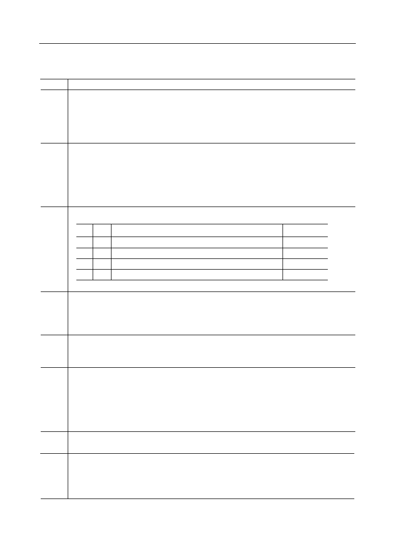
ABSOLUTE MAXIMUM RATINGS
RECOMMENDED OPERATING CONDITIONS
Symbol Rating
*1 : LIM, VR2, TVI, RAI, CMPI
Parameter
Unit
Condition
V
DD
≠0.3 to +7.0
Power Supply Voltage
V
IA
≠0.3 to V
DD
+ 0.3
Analog Input Voltage *1
Ta = 25∞C
Refer to GND
V
ID
Digital Input Voltage *2
V
T
STG
≠55 to +150
Storage Temperature
∞C
--
*2 : SD, EMP, DYN, SEC, RCK1, RCK2, BYP, BR, FDE, BIT, FPS, RVE, PDN, X2, ME, TVE
2.7
3.6
V
DD
V
from
GND level
DYN
= "0"
5.5
V
DD
= 2.7 V to 5.5 V
Parameter
Symbol
Condition
Min.
Typ.
Max.
Unit
Power Supply Voltage
Operating Temperature
Crystal Oscillating Freq.
Data Signaling Rate
C4, C5, C11, C12, C15
C6, C13
C7, C8
C9, C10
C14
C19
C20, C21
T
op
f
X'TAL
T
S
--
--
--
--
--
--
--
--
--
BR = 0"
BR = "1"
--
DYN = "0"
DYN = "1"
--
RL 40kW
--
--
--
DYN= "1"
--
--
--
--
--
--
--
--
--
--
4.5
≠30
3.6860
1.0
0.22
0.47
1.0
0.22
10
0.47
20
2400
1200
5.0
+25
3.6864
--
--
--
--
--
--
--
--
--
--
5.5
+70
3.6868
∞C
MHz
bit/sec
mF
pF
11/25
MSM7557
° Semiconductor
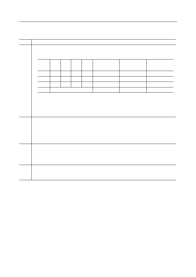
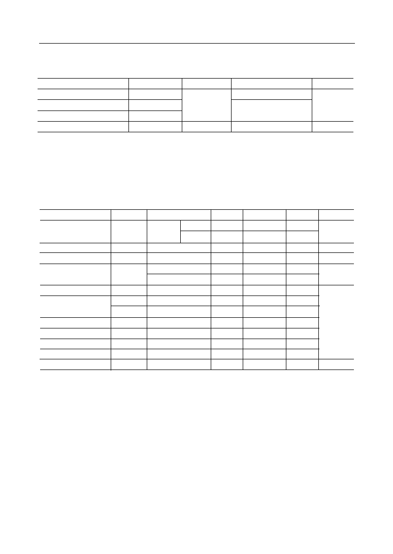
ELECTRICAL CHARACTERISTICS
DC Characteristics
Normal
mode
(mode 4)
DYN = "0" : V
DD
= 2.7 V to 5.5 V, Ta = ≠30∞C to 70∞C
DYN = "1" : V
DD
= 4.5 V to 5.5 V, Ta = ≠30∞C to 70∞C
*1 Refer to PDN pin description
*2 SD, EMP, DYN, SEC, RCK1, RCK2, BYP, BR, FDE, BIT, FPS, RVE, PDN, ME, TVE
*3 ST, FD, RD, RT
Parameter
Symbol
Condition
Min.
Typ.
Max.
Unit
Power Supply Current *1
Input Leakage Current *2
Input Voltege *2
Output Voltege *3
I
DD
I
DDS1
I
DDS2
I
DDS3
I
IL
I
IH
I
IL
I
IH
V
OL
V
OH
Power down
mode 1
Power down
mode 2
Power down
mode 3
3.6 V
5.5 V
5.5 V
3.6 V
V
IN
= 0 V
V
IN
= V
DD
--
I
OL
= ≠20 mA
I
OH
= 20 mA
--
--
--
--
--
≠10
0
0.7V
DD
0
0.8V
DD
9.0
14.0
1.0
3.8
4.6
--
--
--
--
--
18
24
20
7.0
9.0
+10
0.2V
DD
V
DD
0.1V
DD
V
DD
mA
mA
mA
mA
V
12/25
MSM7557
° Semiconductor
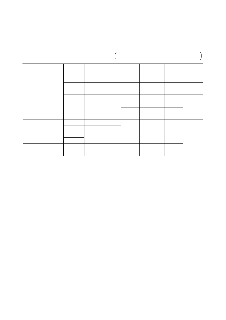
AC Characteristics
1200
bps
2400
bps
--
*1 Receive MSK signal is bit synchronous signal (modulated signal of alternating "0", "1" pattern).
DYN = "0" : V
DD
= 2.7 V to 5.5 V, Ta = ≠30∞C to 70∞C
DYN = "1" : V
DD
= 4.5 V to 5.5 V, Ta = ≠30∞C to 70∞C
Number of data bits
required for the PLL to
be locked in within the
phase difference of
22.5∞ or less
Number of data bits
required for the PLL to
be locked in within the
phase difference of
90∞ or less
Transmit
Carrier Frequency
Transmit
Carrier Level
Receive Carrier
Input Level
Bit Error Rate
Number of PLL Lock-in
Data Bits *1
Parameter
Symbol
Condition
Min.
Typ.
Max.
Unit
f
M1
f
S1
f
M2
f
S2
V
OX
V
IR
B
ER
V
IR
BR
= "0"
SD= "0"
SD
= "1"
SD= "0"
R1
= R2
Defined at
RAIO
ME= "1"
BR
= "1"
ME= "1"
DYN
= "0"
DYN = "1"
8 dB
10 dB
11 dB
13 dB
1199
1799
1199
2399
≠11
≠3
≠32
--
--
--
--
--
1 • 10
-3
1200
1800
1200
2400
≠9
≠1
--
5 • 10
-5
1 • 10
-3
5 • 10
-5
--
--
--
1201
1801
1201
2401
≠7
+1
≠2
--
--
--
18
11
Hz
dBV
--
bit
SD
= "1"
13/25
MSM7557
° Semiconductor
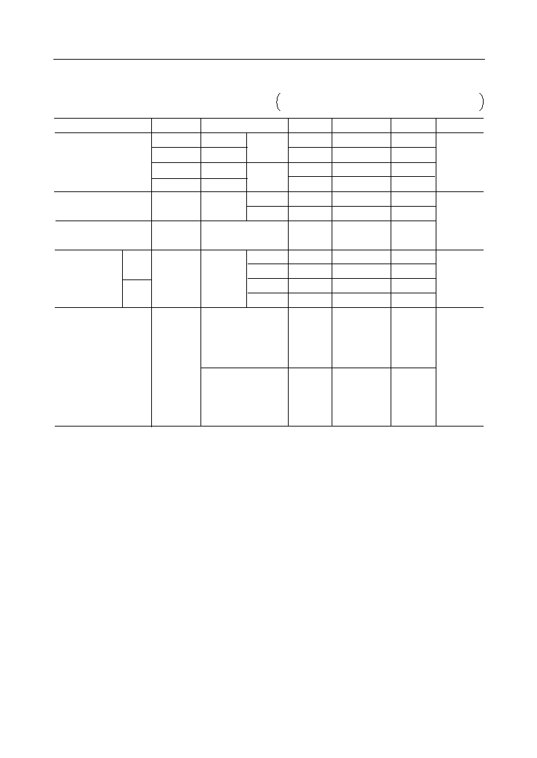
Voice Signal Interfaces
RVO Maximum Output
Signal Level
--
≠6
V
OUT
Min.
--
DYN = "0"
DYN = "1"
DYN = "0"
DYN = "1"
100 Hz
f
IN
= 1 kHz
BYP = "0" *1
R
CV.∆
T
ran.
*1 S/D 20 dB
*2 f
IN
= 1 kHz, BYP = EMP = "1"
*2
Cross Talk
DYN = "0" : V
DD
= 2.7 V to 5.5 V, Ta = ≠30∞C to 70∞C
DYN = "1" : V
DD
= 4.5 V to 5.5 V, Ta = ≠30∞C to 70∞C
Limiter Clamp Level
Transmit Output Distortion
Receive Output Distortion
Transmit Gain
Receive Gain
Transmit Idle Noise
Receive Idle Noise
Transmit Filter
Response
Receive Filter
Response
V
LIM
H
DT
H
DR
G
T
G
R
H
IT
H
IR
C
TT
C
TR
FT1
FT3
FT25
FT34
FT60
FR1
FR3
FR25
FR34
FR60
+2
≠8
0
--
--
+1
+1
--
--
≠60
≠60
≠23
≠8.5
+9.5
+12.5
≠30
+4.5
+11.0
≠6.5
≠8.5
≠30
--
≠9
≠1
≠40
≠40
≠0.2
≠0.2
≠51
≠85
≠75
≠80
≠28
≠10.5
+8.0
+10.5
≠40
+3.0
+9.5
≠8.0
≠10.5
≠40
--
≠10
≠2
--
--
≠1.5
≠1.5
--
--
--
--
--
≠12.5
+6.5
+8.5
--
+1.5
+8.0
≠9.5
≠12.5
--
300 Hz
2.5 kHz
3.4 kHz
6 kHz
100 Hz
300 Hz
2.5 kHz
3.4 kHz
6 kHz
f
IN
= 1 kHz
LIM = open
f
IN
= 1 kHz, ≠12 dBV
BYP = "0", EMP = "1"
f
IN
= 1 kHz, BYP = EMP = "1"
f
IN
= 1 kHz, BYP = EMP = "1"
BYP = "0"
EMP = "1"
RAIO = ≠2 dBV
TVIO = ≠2 dBV
EMP = "1"
BYP = "1"
RCK2 = "0"
Ref. = 1 kHz
EMP = "1"
BYP = "1"
RCK2 = "0"
Ref. = 1 kHz
T
ran.∆
R
CV.
Typ.
Max.
Unit
Condition
Symbol
Parameter
dBV
dB
dBV
dB
14/25
MSM7557
° Semiconductor
(Continued)
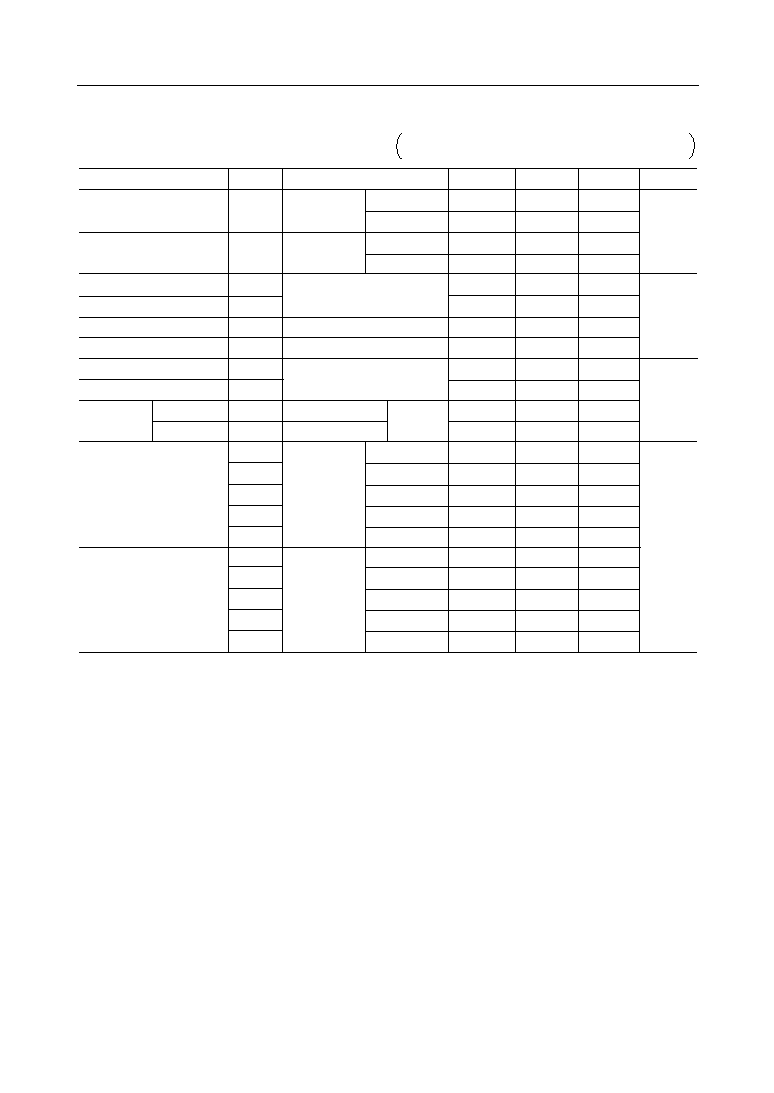
Parameter
Standard Input
Level
f
IN
= 1 kHz
≠13.7
≠11.3
dBV
≠16.1
DYN = "0"
Compressor
Expander
*3 0 dB is defined as the input level and the output level when the standard input
level is input.
*4 V
DD
= 3.6 V, DYN = "0"
*5 V
DD
= 5.0 V, DYN = "0"
*6 V
DD
= 5.0 V, DYN = "1"
DYN = "0" : V
DD
= 2.7 V to 5.5 V, Ta = ≠30∞C to 70∞C
DYN = "1" : V
DD
= 4.5 V to 5.5 V, Ta = ≠30∞C to 70∞C
Maximum Input
Level
Output
Level *3
Attack Time
Recovery Time
Standard Input
Level
Maximum
Output Level
Output
Level
Attack
Time
Recovery
Time
V
ICS
V
ICM
GC2
GC4
GC5
T
AT1
T
AT2
T
RE1
T
RE2
V
IES
V
IEM
GE1
GE2
GE3
T
AT3
T
AT4
T
RE3
T
RE4
f
IN
= 1 kHz
DYN = "0", C6 = 0.22 mF
DYN = "1", C6 = 0.47 mF
DYN = "0", C6 = 0.22 mF
DYN = "1", C6 = 0.47 mF
f
IN
= 1 kHz
f
IN
= 1 kHz *3
DYN = "0", C13 = 0.22 mF
DYN = "1", C13 = 0.47 mF
DYN = "0", C13 = 0.22 mF
DYN = "1", C13 = 0.47 mF
≠3.9
≠7
+1.0
≠9.2
≠18.6
--
--
--
--
--
≠8.7
≠9.1
≠1.5
≠6
+2
≠18.3
≠37.5
--
--
--
--
--
≠5.5
--
--
≠9.9
≠19.8
≠29.5
3.4
3.5
17
16
≠10.8
≠11.2
≠3.1
--
--
≠20
≠40
≠59
3.4
3.5
17
16
≠7.1
--
--
≠10.6
≠21.0
--
--
--
--
--
≠12.9
≠13.3
≠4.7
--
--
≠21.5
≠42.2
--
--
--
--
--
DYN = "1"
DYN = "0"
DYN = "1"
≠20 dB
≠40 dB
≠60 dB
*4
*5
*6
DYN = "0"
DYN = "1"
≠10 dB
≠20 dB
≠30 dB
dB
ms
dBV
dB
ms
Symbol
Condition
Min.
Typ.
Max.
Unit
15/25
MSM7557
° Semiconductor
Common Characteristics
Digital Timing Characteristics
*1 VR1, VR3, TAO, RVO, RAIO
DYN = "0" : V
DD
= 2.7 V to 5.5 V, Ta = ≠30∞C to 70∞C
DYN = "1" : V
DD
= 4.5 V to 5.5 V, Ta = ≠30∞C to 70∞C
Parameter Symbol
Condition
Min.
Typ.
Max.
Unit
Input Resistance
Output Resistance
Output Load Resistance
Output DC Voltage
R
IA
R
IC
R
OX
1
R
OX
2
R
OX
3
RXL1
RXL2
V
SG
V
AO
TVI, RAI, VR2
LIM
TAO
VR1, VR3, RVO
TVIO, RAIO
S/D 20 dB
SG
TAO, RVO
*1
TVIO
--
--
--
--
--
40
60
V
DD
≠ 0.1
2
V
DD
2
V
DD
+ 0.1
2
V
DD
≠ 0.15
2
V
DD
2
V
DD
+ 0.15
2
10
200
1750
600
100
--
--
--
--
--
--
--
--
--
MW
kW
W
kW
V
DYN = "0" : V
DD
= 2.7 V to 5.5 V, Ta = ≠30∞C to 70∞C
DYN = "1" : V
DD
= 4.5 V to 5.5 V, Ta = ≠30∞C to 70∞C
Parameter
Symbol
Condition
Min.
Typ.
Max.
Unit
Transmit Data
Set-up Time
Transmit Data
Hold Time
Receive Data
Output Delay
Sync-signal
Output Delay (ME∆ST)
t
S
t
H
t
D
t
MS
Refer to Fig. 1
Refer to Fig. 1
Refer to Fig. 1
1
1
≠300
0
--
--
--
--
--
--
834
300
ms
ns
ms
16/25
MSM7557
° Semiconductor
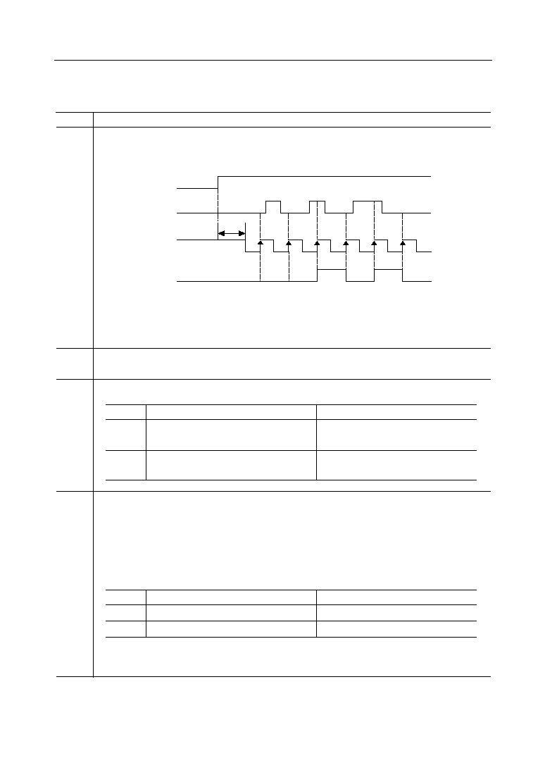
TIMING DIAGRAM
Figure 1 Input Data Timing
Figure 2 Output Data Timing
Figure 3 Receive Signal Timing
RT
FD,RD
50%
50%
t
D
ST
SD
50%
50%
t
H
t
S
FDE
RT
Internal RD
FD
RD
D1
D2
D3
D1
D2
D3
N-2
N-1
N
N-2, N-1, N : Frame shnchronous signal
17/25
MSM7557
° Semiconductor
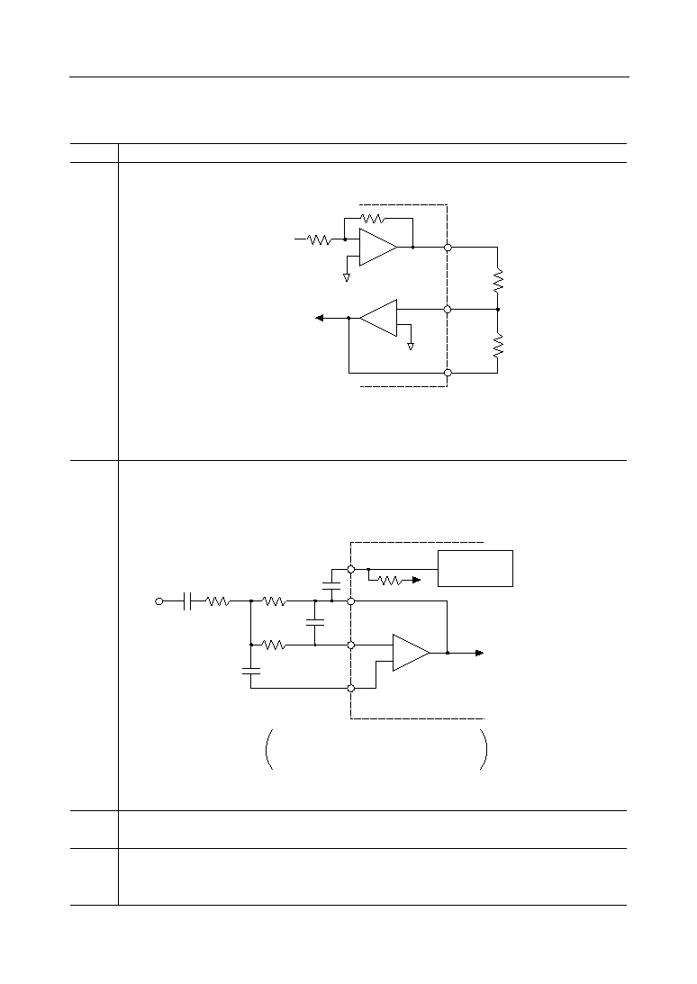
OPERATION DESCRIPTION
Limiter Circuit
A
+
≠
R11
R12
LIM
HPF1 or PRE ≠ EMPHASIS
Limiter
Reverse
Splatter filter
R11 : 1 kW
R12 : 200 kW
DYN = "0"
: Clamp level = VSG
±
0.50 V
DYN = "1"
: Clamp level = VSG
±
1.26 V
2. In case of using external voltage reference
LIM pin shall be supplied over VSG voltage.
Notes
1 ) R11 is protection resister from external extra voltage.
2 ) Resistor value of R11 and R12 changes 0.7 to 1.3 times from the typical value
by lot variation and temperature variation.
18/25
MSM7557
° Semiconductor
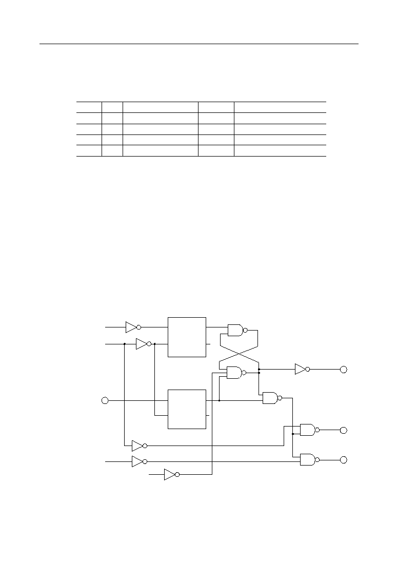
Frame detection pattern is defined by BIT and FPS.
Fig 3 shows detection timing
First, put digital "0" level to FDE pin more than 1 ms, then FD pin is reset to "0" level.
Next, put digital "1" level to FDE pin, then RT and RD output digital "1" level until frame synchronous
signal detected.
When synchronous pattern is detected, FD pin is held to digital "1" level.
At the full power down state (PDN = "1", RVE = "0"), FD pin becomes reset state.
In order to detect frame synchronous signal certainly, receive side PLL should be locked in
sufficiently.
When a modem starts data transmittion, the bit-synchronous signal of more than 18 bits should be
transmitted before frame pattern of the upper table.
Frame Detector
Frame detection signal
FDE
Internal RD
Full power down signal
(Internal signal)
D
Q
Q
CK
FD
RT
RD
D
Q
Q
CK
Internal RT
BIT
FPS
Sync-pattern
Note
M.T. = Master telephone
S.H. = Slave handset
Receiver
0
0
1
1
0
1
0
1
9336H
C4D6H
A9336H
AC4D6H
S.H.
M.T.
S.H.
M.T.
Frame synchronous
Frame synchronous
Bit + Frame synchronous
Bit + Frame synchronous
19/25
MSM7557
° Semiconductor
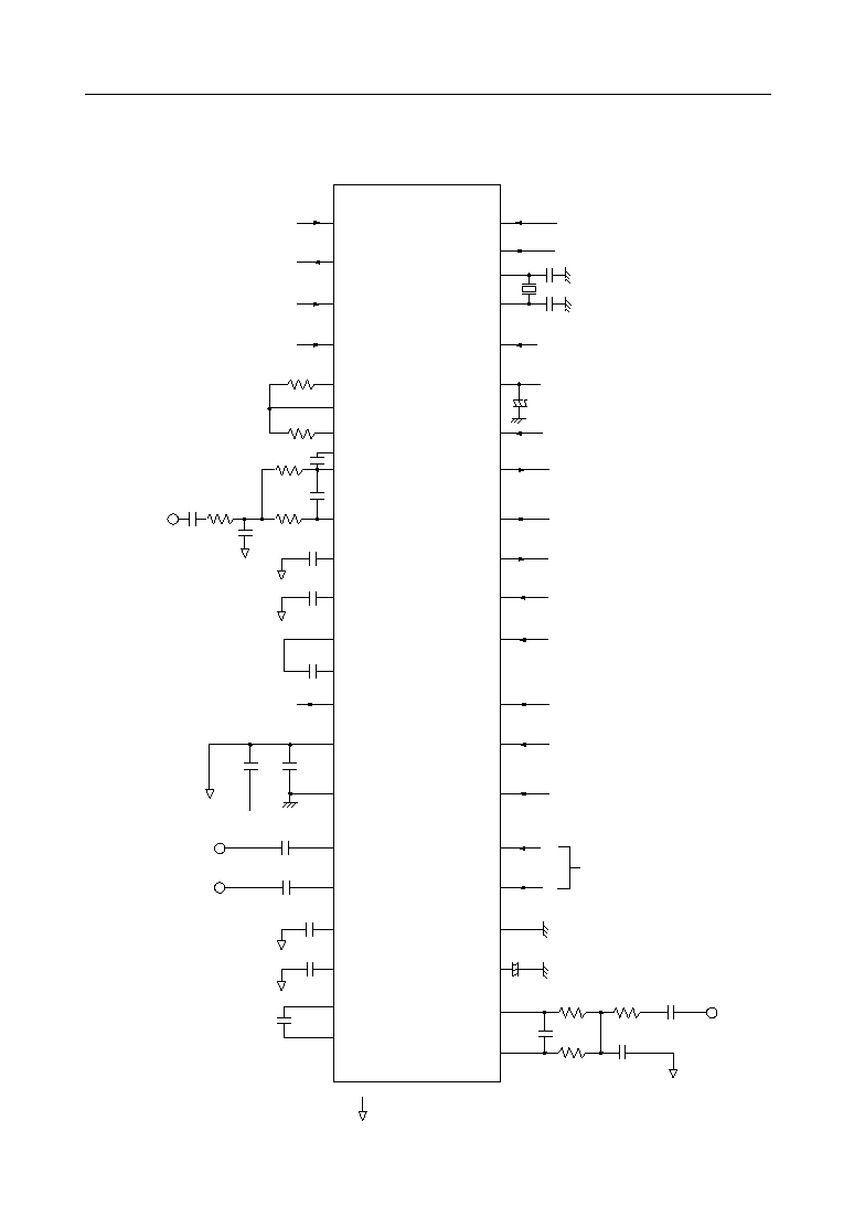
Application Circuit
MSM7557GS-2K
SD
ST
EMP
LIM
TVE
ME
X1
PDN
X2
Transmit data
Transmit data timing clock
Emphasis path select
Limiter circuit
clamp voltage input
R1
R2
C19
R5
C3
R3
C1
C2
R4
C4
C5
C6
Transmit
voice input
VR1
VDD
VR2
VR3
RVE
CMPI
TVIO
RT
TVI
RD
CC1
FD
CC2
FPS
CC3N
FDE
CC3P
BIT
DYN
BR
SG
Dynamic range
select
C7
C8
V
DD
C9
C10
Transmit signal output
Receive voice output
C11
C12
C13
≠
+
C15
C16
R7
R6
R8
C18
C17
Modem data signaling rate select
Frame synchronous detector
control
GND
TAO
RVO
CE1
CE2
CE3N
CE3P
SEC
CSH
Note
: An arrow mark of ( ) indicates connection to the SG pin.
+
≠
Transmit voice output control
MSK modulator control
3.6864 MHz
Power down control
C20
C21
C14
Power supply
Receive voice output control
Receive timing clock
Receive data
Frame synchronous
detector output
Synchronous pattern select
Bit synchronus
detector control
RAIO
RAI
Receive
signal input
RCK1
RCK2
Voice band select
BYP
Compandor path select

20/25
MSM7557
° Semiconductor
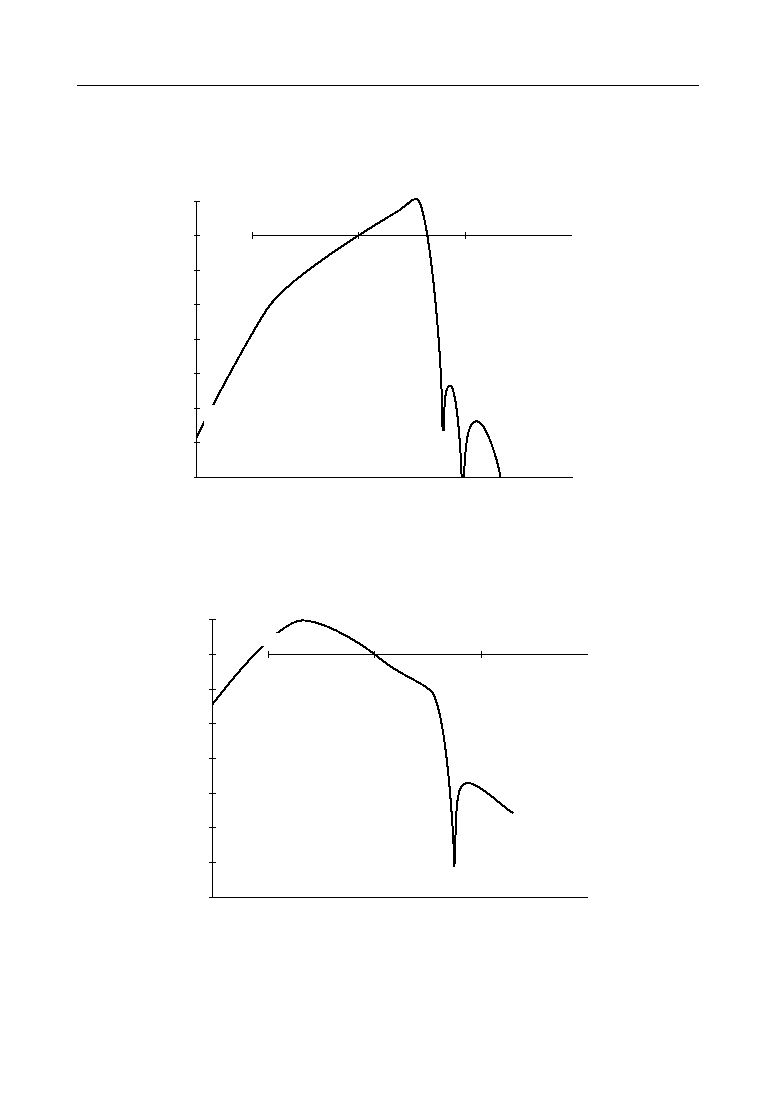
MSM7557 Filter Characteristics
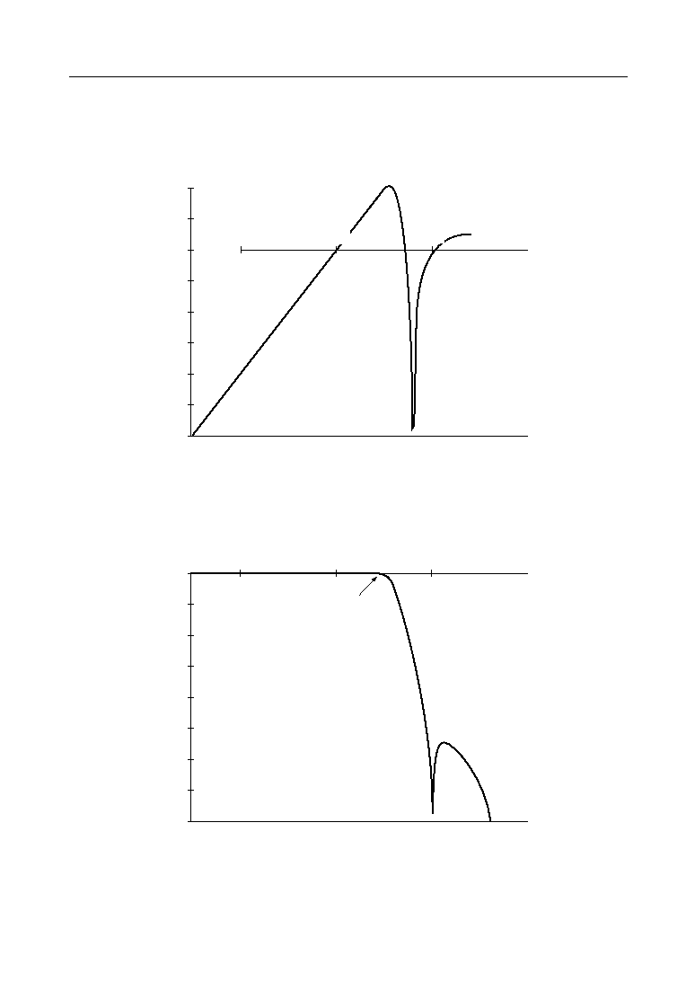
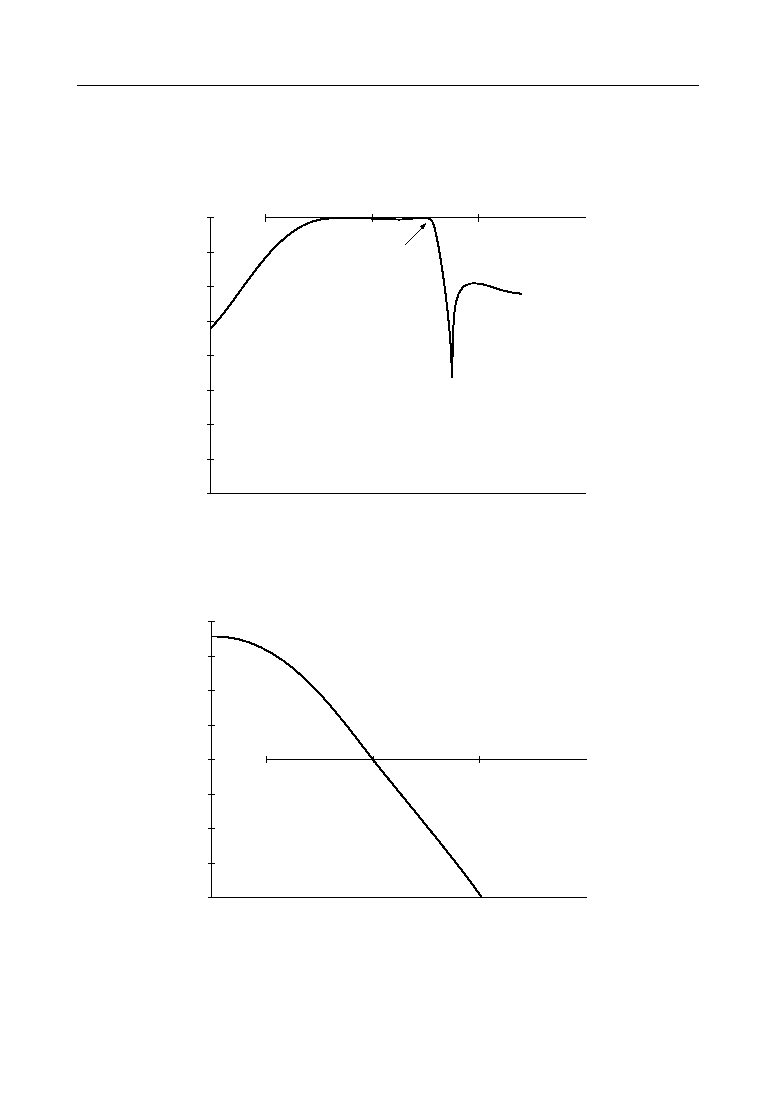
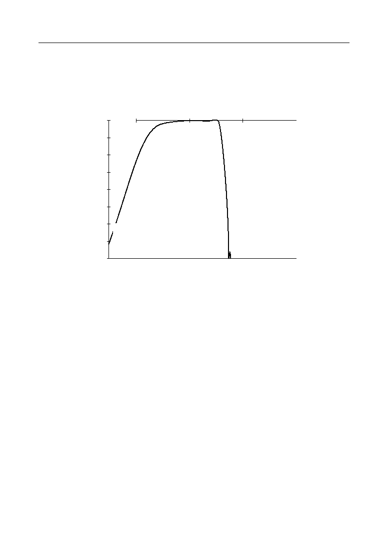
MSM7557 has wide band filters (0.3 kHz to 3.4 kHz) as follows.
Pre-Emphasis ........................................................................................................ Fig. 4
Splatter Filter ........................................................................................................ Fig. 5
RBPF ....................................................................................................................... Fig. 6
De-Emphasis ......................................................................................................... Fig. 7
Transmit Total (HPF1 + Pre-Emphasis + Splatter) ......................................... Fig. 8
Receive Total (RBPF + De-Emphasis) ............................................................... Fig. 9
Transmit and Receive Total ................................................................................ Fig. 10
Fig. 4 to Fig. 10 show the filter characteristics when RCK2 is digital "0". When RCK1 is digital "0" and
RCK2 is digital "1", the filter characteristics change 0.972 times on the frequency axis. (pass-band
becomes narrow) When RCK1 is digital "1" and RCK2 is digital "1", the filter characteristics change
1.029 times on the frequency axis. (pass-band becomes wide)
21/25
MSM7557
° Semiconductor
Figure 4 MSM7557 Pre≠Emphasis
10
0
≠10
≠20
≠30
FREQ [Hz]
LEVEL [dB]
100
1k
10k
Figure 5 MSM7557 Splatter Filter
0
≠10
≠20
≠30
≠40
≠50
≠60
≠70
≠80
FREQ [Hz]
LEVEL [dB]
100
1k
10k
F
cut
(≠0.2 dB) = 3.4 kHz
22/25
MSM7557
° Semiconductor
Figure 6 MSM7557 RBPF
0
≠10
≠20
≠30
≠40
≠50
≠60
≠70
≠80
FREQ [Hz]
LEVEL [dB]
F
cut
(≠0.2 dB) = 3.4 kHz
100
1k
10k
Figure 7 MSM7557 De≠Emphasis
20
10
0
≠10
≠20
FREQ [Hz]
LEVEL [dB]
100
1k
10k
23/25
MSM7557
° Semiconductor
Figure 8 MSM7557 Transmit Total (HPF1 + Pre≠Emphasis+Splatter)
10
0
≠10
≠20
≠30
≠40
≠50
≠60
≠70
FREQ [Hz]
LEVEL [dB]
100
1k
10k
Figure 9 MSM7557 Receive Total (RBPF + De≠Emphasis)
FREQ [Hz]
LEVEL [dB]
100
1k
10k
10
0
≠10
≠20
≠30
≠40
≠50
≠60
≠70
24/25
MSM7557
° Semiconductor
Figure 10 MSM7557 Transmit and Receive Total
FREQ [Hz]
LEVEL [dB]
100
1k
10k
0
≠10
≠20
≠30
≠40
≠50
≠60
≠70
≠80
25/25
MSM7557
° Semiconductor
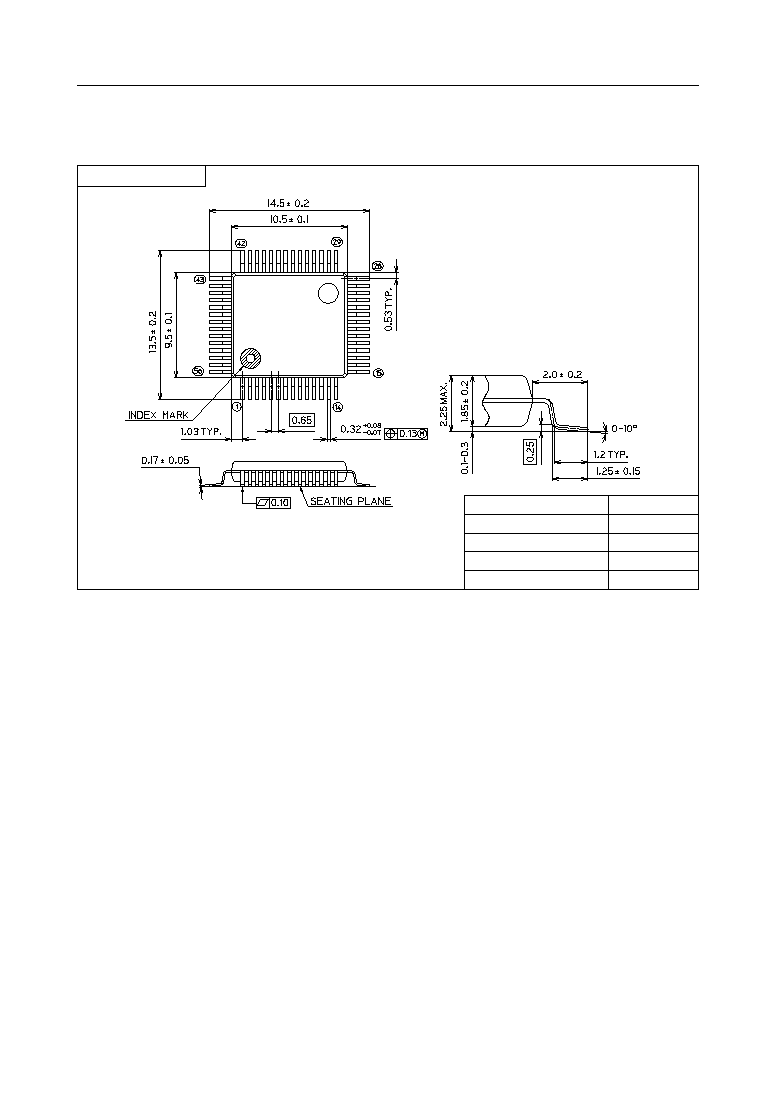
(Unit : mm)
PACKAGE DIMENSIONS
Notes for Mounting the Surface Mount Type Package
The SOP, QFP, TSOP, SOJ, QFJ (PLCC), SHP and BGA are surface mount type packages, which
are very susceptible to heat in reflow mounting and humidity absorbed in storage.
Therefore, before you perform reflow mounting, contact Oki's responsible sales person for the
product name, package name, pin number, package code and desired mounting conditions
(reflow method, temperature and times).
QFP56-P-910-0.65-2K
Package material
Lead frame material
Pin treatment
Solder plate thickness
Package weight (g)
Epoxy resin
42 alloy
Solder plating
5 mm or more
0.43 TYP.
Mirror finish