 | –≠–ª–µ–∫—Ç—Ä–æ–Ω–Ω—ã–π –∫–æ–º–ø–æ–Ω–µ–Ω—Ç: MSM7560L | –°–∫–∞—á–∞—Ç—å:  PDF PDF  ZIP ZIP |

1/15
MSM7540L/7560L
° Semiconductor
° Semiconductor
MSM7540L/7560L
Single Rail ADPCM CODEC
GENERAL DESCRIPTION
The MSM7540L/7560L are single channel ADPCM CODEC ICs which perform mutual transcoding
between an analog voice band signal 300 to 3400 Hz and 32 kbps ADPCM serial data.
Using advanced circuit technology, these devices operate from a single 3 V power supply and
provide low power consumption.
The MSM7540L/7560L are optimized for advanced digital cordless telephone system applications.
FEATURES
∑
∑
∑
∑
∑ Single 3 V Power Supply Operation
∑
∑
∑
∑
∑ ADPCM Algorithm :
Complies completely with 1988's version ITU-T
G.721 (32 kbps)
∑
∑
∑
∑
∑ Transmit/Receive Full-Duplex Operation
∑
∑
∑
∑
∑ Transmit/Receive Synchronous Mode Only
∑
∑
∑
∑
∑ Serial ADPCM Transmission Data Rate :
32 kbps to 2048 kbps
∑
∑
∑
∑
∑ Serial PCM Transmission Data Rate :
64 kbps to 2048 kbps
∑
∑
∑
∑
∑ PCM Interface Coding Format
MSM7540L :
A-law or Linear (14 bit, 2's compliment) Selectable
MSM7560L :
m-law or Linear (14 bit, 2's compliment) Selectable
∑
∑
∑
∑
∑ Low Power Consumption
Operating Mode :
18 mW Typ. (V
DD
= 3.0 V)
Power-Down Mode :
0.3 mW Typ. (V
DD
= 3.0 V)
∑
∑
∑
∑
∑ Two Analog Input Amplifier Stages :
Externally Adjustable Gain
∑
∑
∑
∑
∑ Analog Output Stage :
Push-pull Drive (direct drive of 350 W + 120 nF)
∑
∑
∑
∑
∑ Built-in Crystal Oscillator (10.368 MHz)
∑
∑
∑
∑
∑ Built-in Reference Voltage Supply
∑
∑
∑
∑
∑ Option Reset Specified by ITU-T G. 721/ADPCM
∑
∑
∑
∑
∑ Package:
28-pin plastic SOP
(SOP28-P-430-1.27-K)
(Product name: MSM7540LGS-K)
(Product name: MSM7560LGS-K)
32-pin plastic TSOP
(TSOPI32-P-814-0.50-1K) (Product name: MSM7560LTS-K)
E2U0027-28-83
This version: Aug. 1998
Previous version: Nov. 1996
2/15
MSM7540L/7560L
° Semiconductor
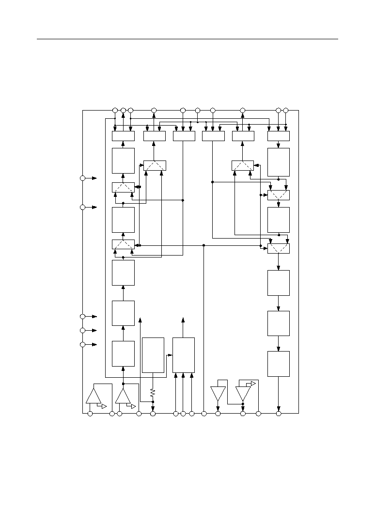
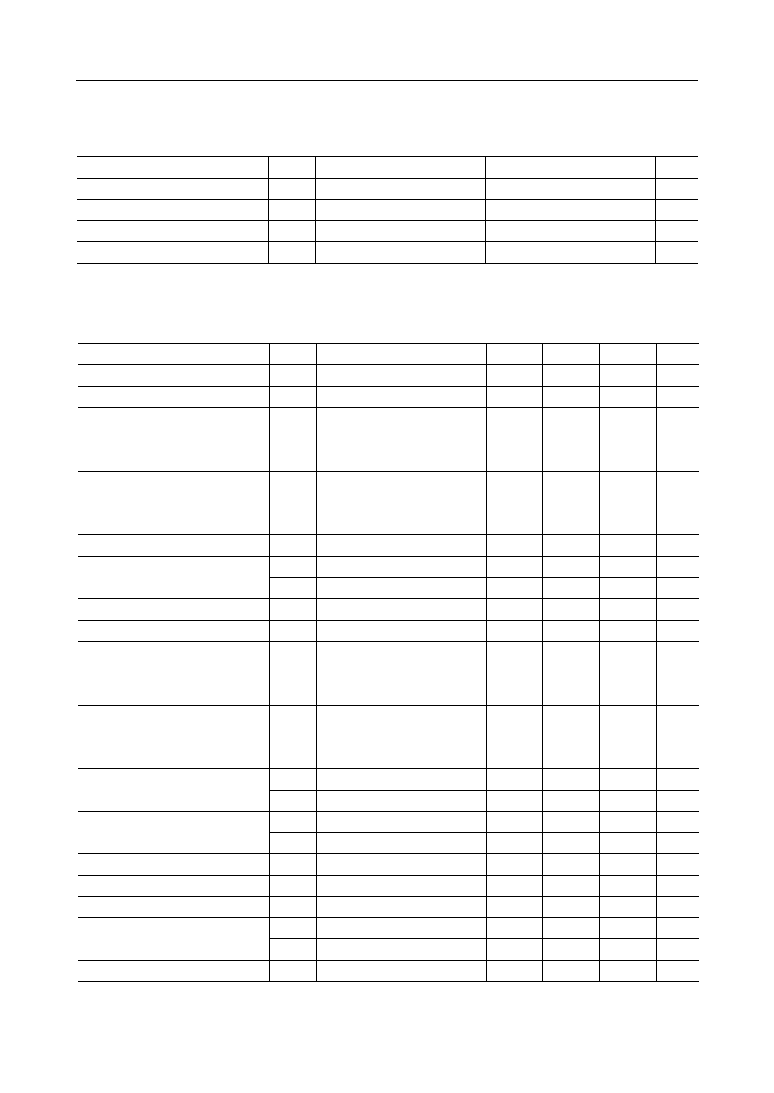
AIN2
GSX2
XSYNC
IS
AIN1
GSX1
AOUT≠
ADPCM
CODER
1
0
V
DD
BCLKA
0
1
PCMSO
PCMSI
PCMRI
PCMRO
IR
RSYNC
0
1
ADPCM
DECODER
1
0
BCLKB
AG DG
X1
X2
PWI
V
REF
SG
CLOCK/
TIMING
MCK
LPS
RES
PDN
AOUT+
≠
+
≠1
VFRO
≠
+
≠
+
P
/
S
P
/
S
S
/
P
S
/
P
P
/
S
S
/
P
0
1
RC-
LPF
A/D
Conv.
BPF
EX-
PANDER
1
0
RC-
LPF
D/A
Conv.
LPF
COM-
PANDER
BLOCK DIAGRAM
3/15
MSM7540L/7560L
° Semiconductor
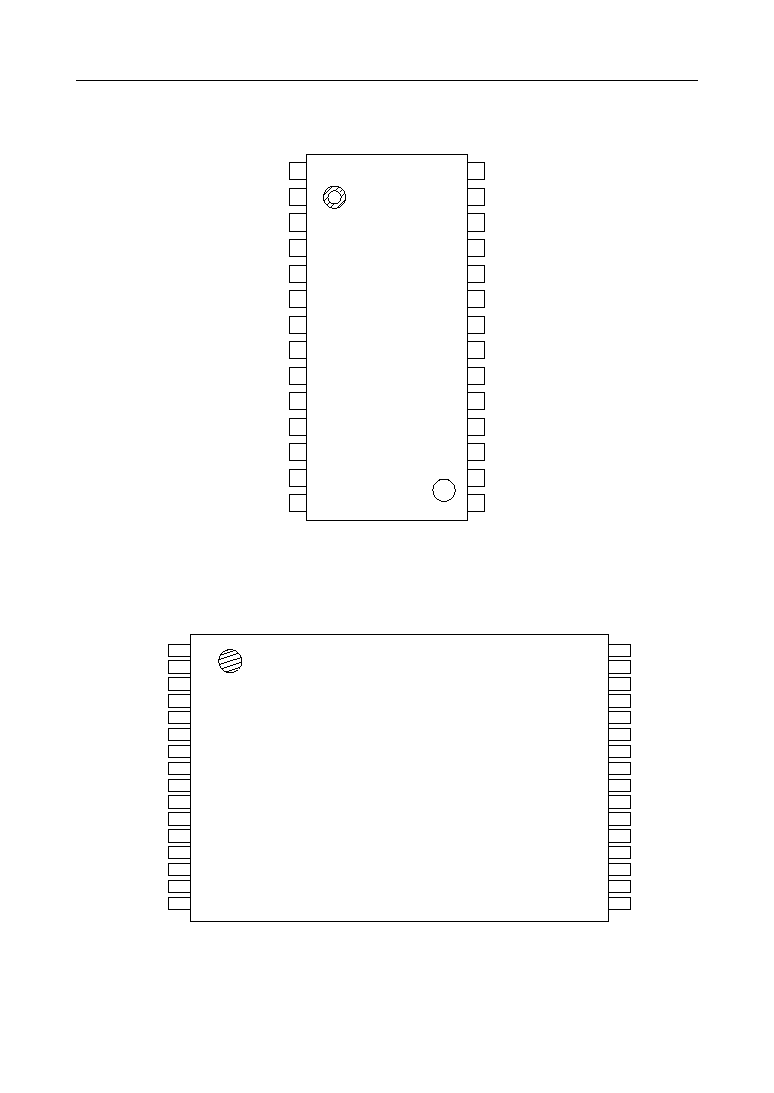
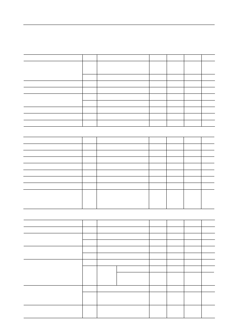
PIN CONFIGURATION (TOP VIEW)
1
2
3
4
5
6
7
8
9
10
11
12
13
14
15
16
17
18
19
20
21
22
23
24
25
26
27
28
RES
PCMRI
PCMRO
IR
IS
PCMSI
PCMSO
LPS
DG
AG
SG
AIN1
GSX1
AIN2
GSX2
VFRO
PWI
AOUT≠
AOUT+
V
DD
PDN
X1
X2
MCK
RSYNC
XSYNC
BCLKA
BCLKB
28-Pin Plastic SOP
1
2
3
4
5
6
7
8
9
10
11
12
13
14
15
16
32
31
30
29
28
27
26
25
24
23
22
21
20
19
18
17
X1
X2
NC
MCK
RSYNC
XSYNC
BCLKA
BCLKB
RES
PCMRI
PCMRO
IR
IS
NC
PCMSI
PCMSO
PDN
V
DD
NC
AOUT+
AOUT≠
PWI
VFRO
GSX2
AIN2
GSX1
AIN1
SG
AG
NC
DG
LPS
NC: No connection
32-Pin Plastic TSOP
4/15
MSM7540L/7560L
° Semiconductor
PIN AND FUNCTIONAL DESCRIPTIONS
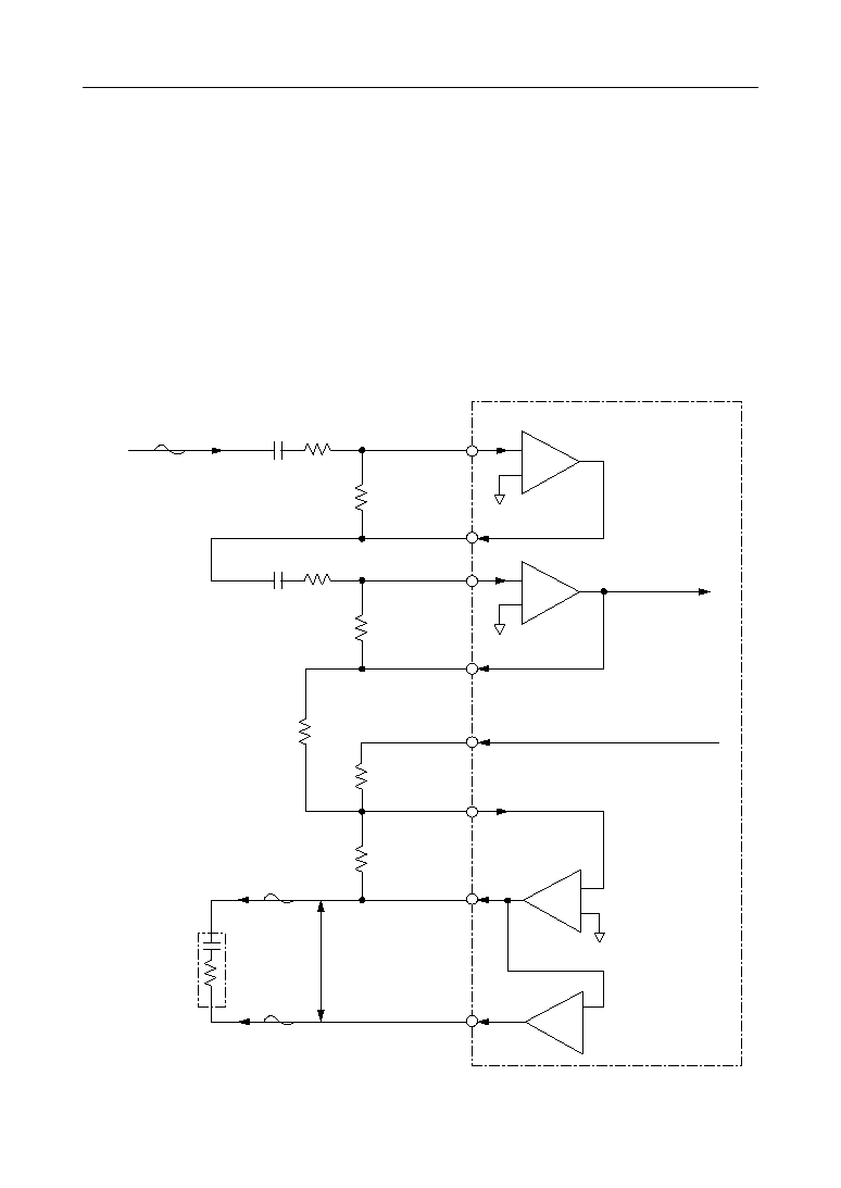
AIN1, AIN2, GSX1, GSX2
Transmits analog input and the output for transmit gain adjustment.
AIN1 (AIN2) connects to the inverting input of the internal transmit amplifier. GSX1 (GSX2)
connects to the output of the internal transmit amplifier output. Refer to Fig. 1 for gain
adjustment.
VFRO, AOUT+, AOUT≠, PWI
Receives analog output and the output for receive gain adjustment.
VFRO is receive filter output. AOUT+ and AOUT≠ are differential analog signal outputs which
can directly drive Z
L
= 350 W + 120 nF. Refer to Fig. 1 for gain adjustment.
Figure1 Analog Input/Output Interface
AIN1
GSX1
Analog Input
R2
C1
to ENCODER
R1
from DECODER
Analog Output
Z
L
=120 nF
+ 350
W
*: Side Tone Pass (Gain = R6/RS)
AIN2
GSX2
R4
C2
R3
AOUT≠
PWI
R6
RS*
VFRO
R5
≠1
AOUT+
≠
+
≠
+
≠
+
Transmit Gain:
= (R2/R1)
• (R4/R3)
Receive Gain:
= (R6/R5)
V
0

5/15
MSM7540L/7560L
° Semiconductor
SG
Analog signal ground voltage output.
The output voltage of this pin is approximately 1.4 V. Put bypass capacitors between this pin
and the AG pin. During power-down this output voltage is 0 V. The external SG voltage, if
necessary, should be used via a buffer.
AG
Analog ground.
DG
Digital ground.
This ground is separated internally from the analog signal ground pin (AG). The DG pin must
be kept as close as possible to AG on the PCB.
V
DD
+3 V power supply.
LPS
PCM coding law selection.
MSM7540L only; if this pin goes to a "0" level, PCMSO, PCMSI, PCMRO, and PCMRI become the
A-law character signal, and if these pins goes to a "1" level, the signal becomes a linear value
character signal (2's complement).
MSM7560L only; if this pin goes to a "0" level, PCMSO, PCMSI, PCMRO, and PCMRI become the
m-law character signal, and if these pins goes to a "1" level, the signal becomes a linear value
character signal (2's complement).
PDN
Power down control input.
If this pin is "0", this device is in the power-down state.
Normally, this pin is set to "1".
RES
Optional reset input specified by ITU-T Recommendation G. 721.
If this pin is "0", the device is in the reset state. The reset width (during "L") should be 125 ms or
more.
MCK
Master clock input.
The frequency must be 10.368 MHz. The master clock signal may be asynchronous to BCLKA,
BCLKB, XSYNC, and RSYNC.
PCMSO
Transmit PCM data output.
PCM is output from MSB in synchronization with the rising edge of BCLKB and XSYNC.

6/15
MSM7540L/7560L
° Semiconductor
PCMSI
Transmit PCM data input.
This signal is converted to transmit ADPCM data. PCM is shifted in synchronization with the
falling edge of BCLKB. Normally, this pin is connected to PCMSO.
PCMRO
Receive PCM data output.
PCM is the output signal after ADPCM decoder processing. This signal is output serially from
MSB in synchronization with the rising edge of BCLKB and RSYNC.
PCMRI
Receive PCM data input.
PCM is shifted on the falling edge of the BCLKB input from MSB. Normally, this pin is connected
to PCMRO.
IS
Transmit ADPCM signal output.
After having encoded PCM with ADPCM, this signal is output from MSB in synchronization
with the rising edge of BCLKA and XSYNC. This pin is an open drain output and remains in a
high impedance state during power-down. IS requires a pull-up resistor.
IR
Receive ADPCM signal input.
The ADPCM signal is shifted in series and synchronization with the falling edge of BCLKA and
RSYNC and output from MSB.
BCLKB
Shift clock input for the PCM data (PCMSO, PCMSI, PCMRO, PCMRI).
The frequency is set in the 64 kHz to 2048 kHz range.
XSYNC
8 kHz synchronous signal input for transmit PCM and ADPCM data.
Synchronize this signal with BCLKA and BCLKB signal. XSYNC is used to indicate the MSB of
the serial PCM and ADPCM data stream.
Be sure to input the XSYNC signal because it is also used as the imput of the timing generator.
RSYNC
8 kHz synchronous signal input for receive PCM and ADPCM data.
Synchronize this signal with BCLKA and BCLKB signal. RSYNC is used to indicate the MSB of
the serial PCM and ADPCM data stream.
BCLKA
Shift clock input for the ADPCM data (IS, IR).
The frequency is set in the of 32 kHz to 2048 kHz range.
7/15
MSM7540L/7560L
° Semiconductor
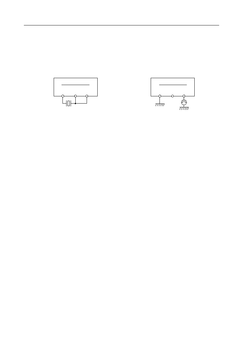
X1, X2
Crystal oscillator (10.368 MHz) connection.
Connect X2, the clock output pin, directly to the MCK pin.
When using a conventional external clock of 10.368 MHz, X1 should be connected to the ground,
X2 open, and provide the external clock through the MCK pin.
X1
MCK
10.368 MHz
<Using a self-oscilation circuit>
X2
MSM7540L/60L
X1
MCK
<Using an external clock>
X2
MSM7540L/60L
10.368 MHz
8/15
MSM7540L/7560L
° Semiconductor
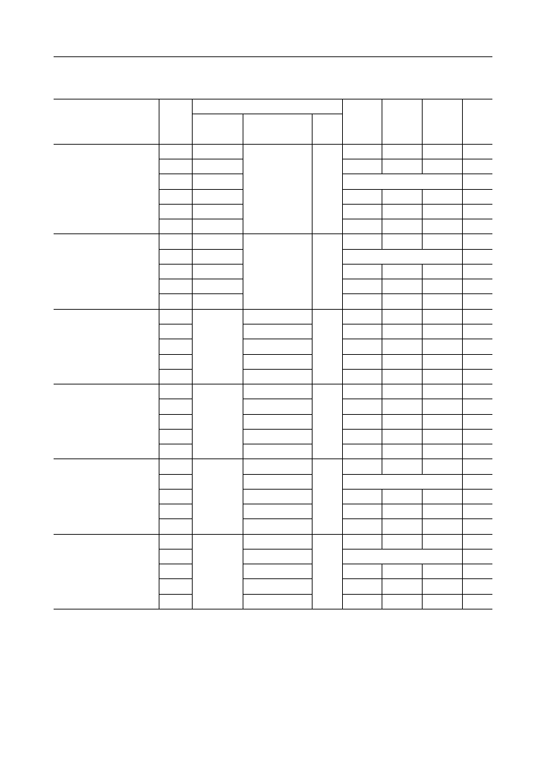
ABSOLUTE MAXIMUM RATINGS
Parameter
Power Supply Voltage
Analog Input Voltage
Digital Input Voltage
Storage Temperature
Symbol
V
DD
V
AIN
V
DIN
T
STG
Condition
--
--
--
--
Rating
≠0.3 to +5
≠0.3 to V
DD
+ 0.3
≠0.3 to V
DD
+ 0.3
≠55 to +150
Unit
V
V
V
∞C
RECOMMENDED OPERATING CONDITIONS
Parameter
Symbol
Condition
Min.
Typ.
Max.
Unit
Power Supply Voltage
V
DD
Voltage must be fixed
2.7
--
3.6
V
MCK, XSYNC, RSYNC, PCMRI,
PCMSI, BCLKA, BCLKB, IR,
LPS, PDN, RES
Input High Voltage
V
IH
0.45
• V
DD
--
V
DD
V
MCK, XSYNC, RSYNC, PCMRI,
PCMSI, BCLKA, BCLKB, IR,
LPS, PDN, RES
Input Low Voltage
V
IL
0
--
0.16
• V
DD
V
Master Clock Frequency
f
MCK
MCK
≠0.01%
10.368
+0.01%
MHz
Bit Clock Freqency
f
BCKA
BCLKA
32
--
2048
kHz
f
BCKB
BCLKB
64
--
2048
kHz
Synchronous Signal Frequency
f
SYMC
XSYNC, RSYNC
--
8.0
--
kHz
Clock Duty Ratio
D
C
MCK, BCLKA, BCLKB
30
50
70
%
MCK, XSYNC, RSYNC, PCMRI,
PCMSI, BCLKA, BCLKB, IR,
LPS, PDN, RES
Digital Input Rise Time
t
Ir
--
--
50
ns
MCK, XSYNC, RSYNC, PCMRI,
PCMSI, BCLKA, BCLKB, IR,
LPS, PDN, RES
Digital Input Fall Time
t
If
--
--
50
ns
Transmit Sync Signal Setting Time
t
XS
BCLKA, BCLKB to XSYNC
100
--
--
ns
t
XS
XSYNC to BCLKA, BCLKB
100
--
--
ns
Receive Sync Signal Setting Time
t
RS
BCLKA, BCLKB to RSYNC
100
--
--
ns
t
SR
RSYNC to BCLKA, BCLKB
100
--
--
ns
Synchronous Signal Width
t
WS
XSYNC, RSYNC
1 BCLK
--
100
ms
PCM, ADPCM Set-up Time
t
DS
--
100
--
--
ns
PCM, ADPCM Hold Time
t
DH
--
100
--
--
ns
Digital Output Load
R
DL
IS (Pull-up Resistor)
500
--
--
W
C
DL
--
--
100
pF
IS, PCMSO, PCMRO
Operating Temperature
Ta
≠25
+25
+75
∞C
--
Bypass Capacitor for SG
C
SG
--
10+0.1
--
mF
SG
¥GND
9/15
MSM7540L/7560L
° Semiconductor
Parameter
Input Resistance
Output Load Resistance
Output Capacitance
Symbol
R
INPW
R
LVF
R
LAO
C
LVF
C
LAO
Condition
PWI
Min.
10
50
1.2
--
--
Typ.
--
--
--
--
--
Max.
--
--
--
100
100
Unit
M
W
k
W
k
W
pF
pF
VFRO
Output Voltage Level
Offset Voltage
V
OVF
V
OAO
V
OFVF
V
OFAO
--
--
≠100
≠20
--
--
--
--
*1.300
+100
+20
V
PP
V
PP
mV
mV
VFRO,
AOUT+, AOUT≠
VFRO
AOUT+, AOUT≠
AOUT+,
AOUT≠
VFRO
AOUT+, AOUT≠ (GAIN = 0 dB),
Power amp only
G
DB
40
--
--
dB
Power amp (0.3 to 3.4 kHz,
Z
L
= 350
W + 120 nF)(See Fig.1)
R
L
= 50 k
W
Z
L
= 350
W
+ 120 nF(See Fig.1)
R
L
= 1.2 k
W
--
--
V
PP
*1.300
*1.300
Open Loop Gain
ELECTRICAL CHARACTERISTICS
DC and Digital Interface Characteristics
Parameter
Power Supply Current
Input High Voltage
Input Low Voltage
Output Low Voltage
Output Leakage Current
Input Capacitance
Symbol
I
DD1
I
DD2
V
IH
V
IL
V
OL
I
O
Condition
Operating Mode,
Power Down Mode (V
DD
= 3.0 V)
--
--
1 LSTTL, Pull-up: 500
W
IS
Min.
--
--
0.45
• V
DD
0.0
0.0
--
Typ.
6
0.1
--
--
0.2
--
Max.
12
0.2
V
DD
0.16
• V
DD
0.4
10
Unit
mA
mA
V
V
V
mA
C
IN
--
--
5
--
pF
(V
DD
=
2.7 V to 3.6 V, Ta = ≠25∞C to +70∞C)
Input Leakage Current
I
IH
I
IL
V
I
=
V
DD
V
I
=
0 V
--
--
--
--
2.0
0.5
mA
mA
No Signal (V
DD
= 3.0 V)
Transmit Analog Interface Characteristics
Parameter
Input Resistance
Output Load Resistance
Output Load Capacitance
Output Amplitude
Input Offset Voltage
Symbol
R
INX
R
LGX
C
LGX
V
OGX
V
OFGX
Condition
AIN1, AIN2
Min.
10
20
--
--
≠20
Typ.
--
--
--
--
--
Max.
--
--
100
*1.300
+20
Unit
M
W
k
W
pF
V
PP
mV
GSX1, GSX2
GSX1, GSX2
GSX1, GSX2, R
L
= 20 k
W
Pre≠OPAMPs
SG Output Voltage
V
SG
--
1.4
--
V
SG Output Inpedance
R
SG
--
40
80
k
W
SG Rise Time
T
SG
--
700
--
ms
GND
¥SG 10 mF + 0.1 mF
(Rise Time to 90% of max.
level)
--
--
Receive Analog Interface Characteristics
*
≠7.7 dBm (600 W) = 0 dBm0, + 3.14 dBm0 = 1.300 V
PP
(MSM7540L)
≠7.7 dBm (600 W) = 0 dBm0, + 3.17 dBm0 = 1.300 V
PP
(MSM7560L)
10/15
MSM7540L/7560L
° Semiconductor
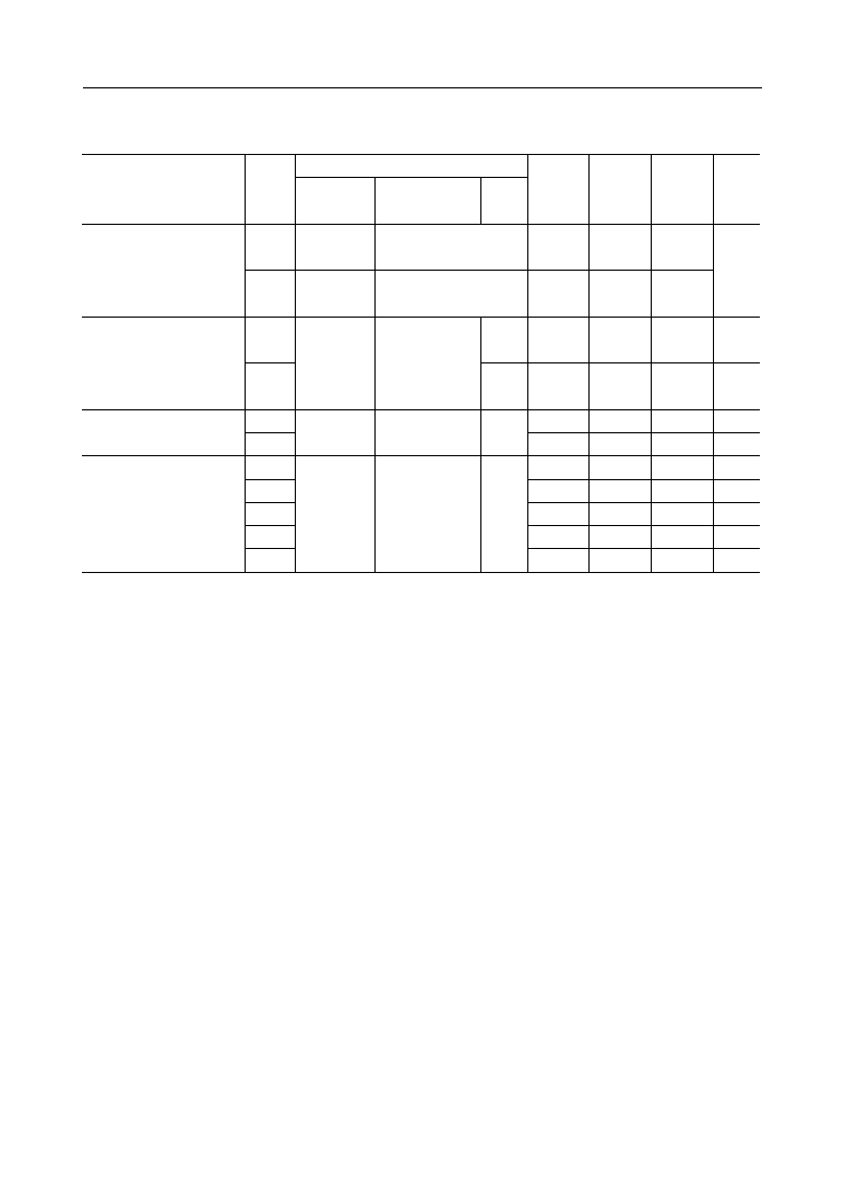
AC Chracteristics
Parameter
Transmit Frequency
Response
Symbol
L
OSS
T1
Level
0 to 60
Min.
25
Typ.
--
Max.
--
Unit
dB
Freq.
Others
L
OSS
T2 300 to 3000
≠0.15
--
+0.20
dB
L
OSS
T3
1020
Reference
dB
0
L
OSS
T4
3300
≠0.15
--
+0.80
dB
L
OSS
T5
3400
0
--
0.80
dB
L
OSS
T6
3968.75
13
--
--
dB
Receive Frequency
Response
0 to 3000
≠0.15
--
+0.20
dB
1020
Reference
dB
3300
≠0.15
--
+0.80
dB
0
3400
0
--
0.80
dB
3968.75
13
--
--
dB
Transmit Signal
to Distortion Ratio
SD T1
35
--
3
SD T2
35
--
0
SD T3
35
--
≠30
SD T4
1020
28
--
≠40
SD T5
23
--
≠45
Receive Signal
to Distortion Ratio
SD R1
--
3
SD R2
--
0
SD R3
--
≠30
SD R4
1020
--
≠40
SD R5
--
≠45
Transmit Gain
Tracking
GT T1
≠0.2
+0.2
GT T2
Reference
GT T3
1020
≠0.2
+0.2
≠40
GT T4
≠0.5
+0.5
GT T5
≠1.2
+1.2
3
≠10
≠50
≠55
Receive Gain
Tracking
GT R1
≠0.2
+0.2
GT R2
Reference
GT R3
1020
≠0.2
+0.2
GT R4
≠0.5
+0.5
GT R5
≠1.2
+1.2
≠40
3
≠10
≠50
≠55
Condition
L
OSS
R1
L
OSS
R2
L
OSS
R3
L
OSS
R4
L
OSS
R5
35
35
35
28
23
--
--
--
--
--
--
--
--
--
--
--
--
--
--
--
--
--
--
(*1)
(*1)
--
--
--
--
dB
dB
dB
dB
dB
dB
dB
dB
dB
dB
dB
dB
dB
dB
dB
dB
dB
dB
dB
dB
(V
DD
=
2.7 V to 3.6 V, Ta = ≠25∞C to +70∞C)
(dBm0)
(Hz)
*1 Use the P-message weighted filter
11/15
MSM7540L/7560L
° Semiconductor
Digital Output
Delay Time
t
SDX
50
--
200
t
SDR
50
--
200
t
XD1
50
--
200
t
XD2
50
--
200
ns
1 LSTTL + 100 pF,
Pull-up: 500
W
P
SRRT
Noise Freq.
: 0 to 50 kHz
30
--
--
dB
Power Supply Noise
Rejection Ratio
Noise Level
: 50 mV
PP
--
P
SRRR
t
XD3
50
--
200
Parameter
Symbol
Level
Min.
Typ.
Max.
Unit
(V
DD
=
2.7 V to 3.6 V, Ta = ≠25∞C to +70∞C)
Freq.
Others
Condition
--
30
--
--
dB
ns
ns
ns
ns
(dBm0)
(Hz)
N
IDLT
--
--
--
≠68
(≠75.7)
dBm0p
(dBmp)
N
IDLR
--
--
1020
A
VT
0.285
0.320
(*3)
0.359
0
A
VR
0.285
0.320
(*3)
0.359
--
≠72
(≠79.7)
Idle Channel Noise
AIN = SG
(*1)
(*2)
Vrms
Vrms
GSX2
Absolute Signal
Amplitude
VFRO
(*1)
--
--
AC Characteristics (Continued)
*1 Use the P-message weighted filter
*2 PCMRI input code
"11010101"(MSM7540L)
"11111111"(MSM7560L)
*3 0.320 Vrms = 0 dBm0 = ≠7.7 dBm
Note: All ADPCM coder and decoder characteristics comply with ITU-T Recommendation
G.721.
12/15
MSM7540L/7560L
° Semiconductor
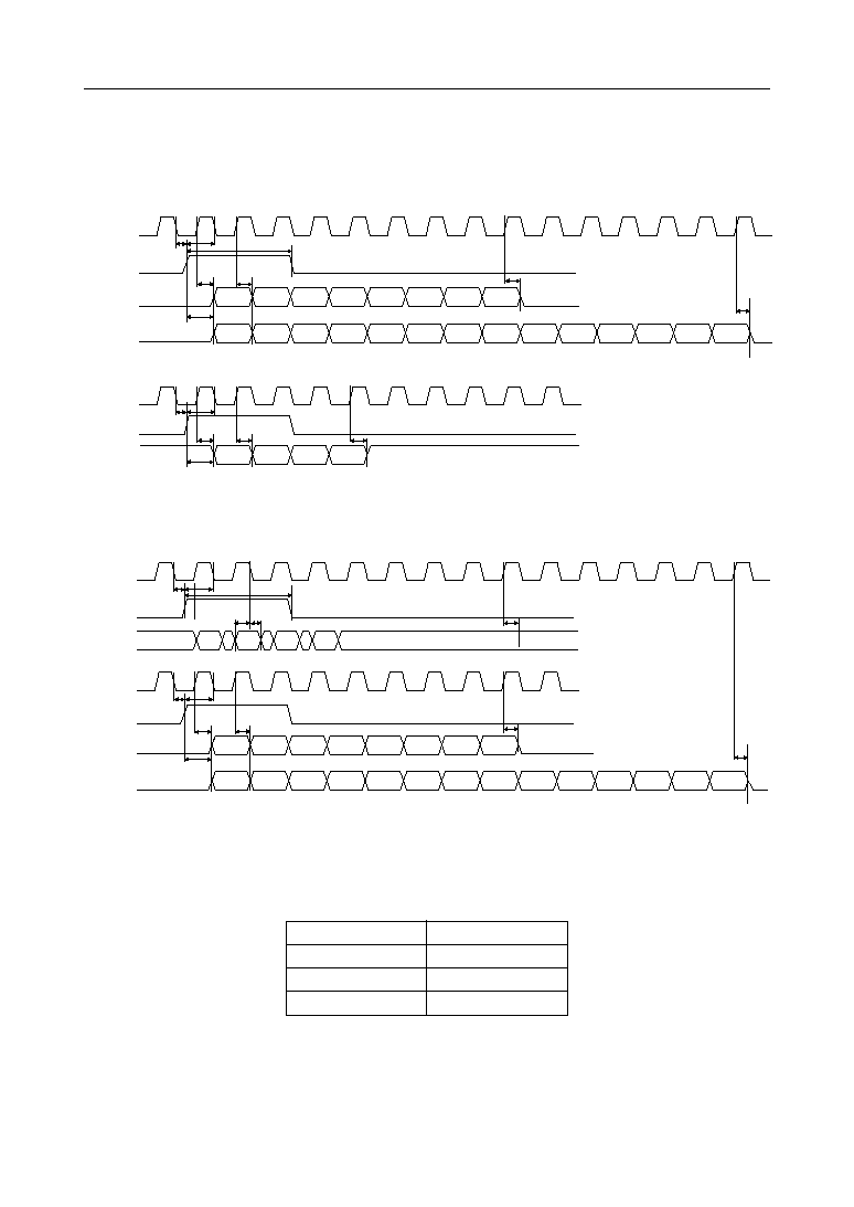
TIMING DIAGRAM
Transmit Side PCM/ADPCM Data Interface
Receive Side PCM/ADPCM Data Interface
MSB
MSB
LSB
LSB
0
1
2
3
4
5
6
7
8
9
10
0
1
2
3
4
5
6
7
8
9
10
11
12
13
txs
tsx
txd1
txd2
tsdx
txs
tsx
txd1
txd2
tsdx
txd3
MSB
LSB
txd3
txd3
BCLKB
XSYNC
PCMSO
PCMSO
(during linear)
BCLKA
XSYNC
IS
14
tws
MSB
MSB
LSB
LSB
0
1
2
3
4
5
6
7
8
9
10
0
1
2
3
4
5
6
7
8
9
10
11
12
13
tsr
tds
tdh
txd3
txd3
trd3
trs
tsr
trd1
trd2
BCLKA
RSYNC
IR
BCLKB
RSYNC
PCMRO
PCMRO
(during linear)
14
tsdx
trs
MSB
LSB
tws
Note: Linear format
A code of an input/output level is determined by the 14-bit 2'compliment.
Refer to the table below for code format.
Input/Output level
+Full-scall
0
≠Full-scall
MSB to LSB
01111111111111
00000000000000
10000000000000
13/15
MSM7540L/7560L
° Semiconductor
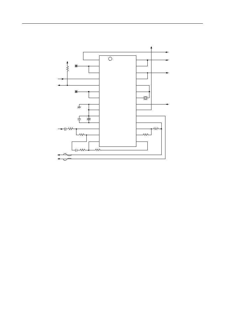
APPLICATION CIRCUIT
MSM7540L/7560L
28
27
26
25
24
23
22
21
20
16
17
19
18
1
2
3
4
5
6
7
8
9
14
13
10
11
8 kHz Sync Signal Input
Power Down Input
Receive ADPCM Input
Transmit ADPCM Output
Transmit Analog Input
Receive Analog Output
(Push-Pull)
V
DD
V
DD
ADPCM Algorithm
Reset Input
Shift Clock Input for
PCM, ADPCM Data
(64 kHz to 2048 kHz)
10.368 MHz
Receive
PCM Output
Transmit
PCM Output
15
AIN2
GSX2
GSX1
VFRO
AIN1
PWI
SG
AOUT≠
RES
PCMRI
PCMRO
IR
IS
PCMSI
PCMSO
LPS
DG
BCLKB
BCLKA
XSYNC
RSYNC
MCK
X2
X1
PDN
V
DD
AG
AOUT+
12
14/15
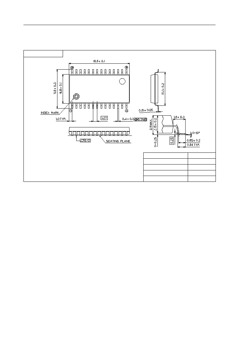
MSM7540L/7560L
° Semiconductor
(Unit : mm)
PACKAGE DIMENSIONS
Notes for Mounting the Surface Mount Type Package
The SOP, QFP, TSOP, SOJ, QFJ (PLCC), SHP and BGA are surface mount type packages, which
are very susceptible to heat in reflow mounting and humidity absorbed in storage.
Therefore, before you perform reflow mounting, contact Oki's responsible sales person for the
product name, package name, pin number, package code and desired mounting conditions
(reflow method, temperature and times).
SOP28-P-430-1.27-K
Package material
Lead frame material
Pin treatment
Solder plate thickness
Package weight (g)
Epoxy resin
42 alloy
Solder plating
5
mm or more
0.75 TYP.
Mirror finish
15/15
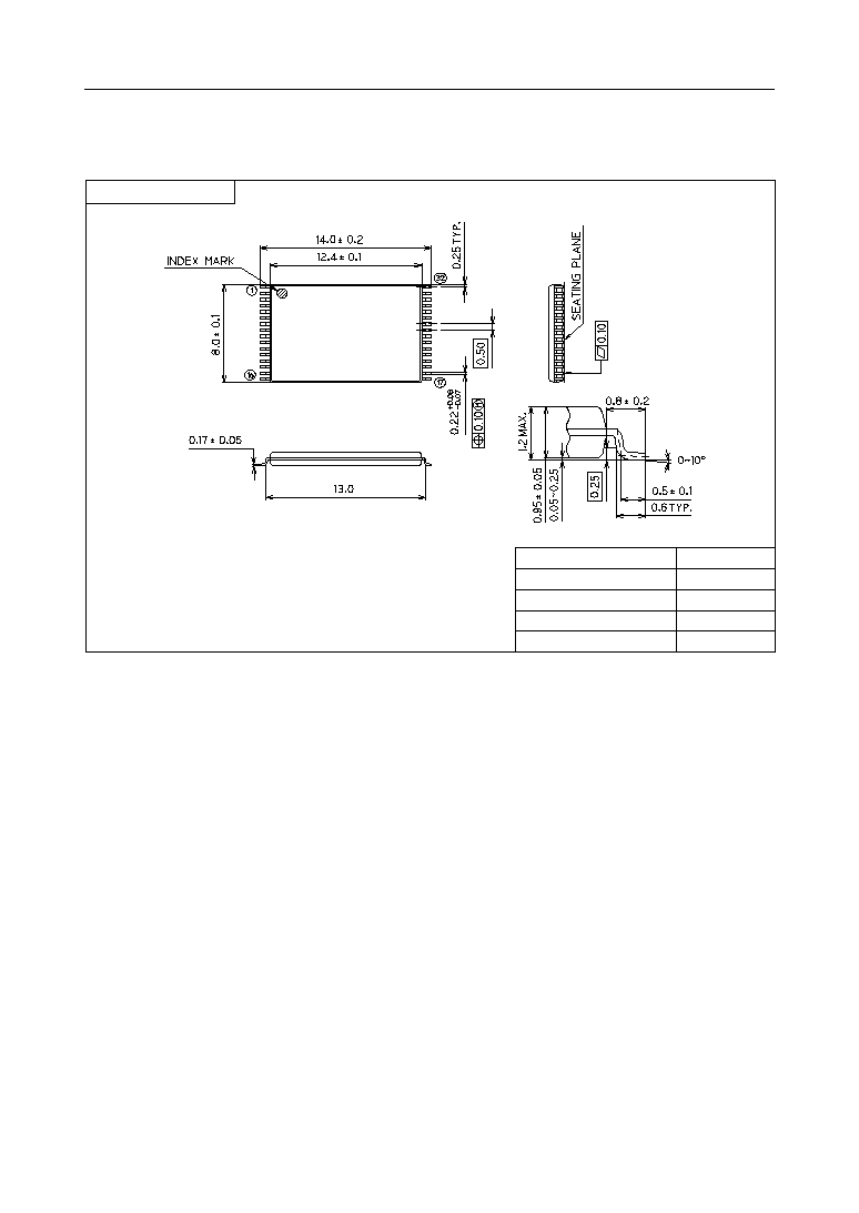
MSM7540L/7560L
° Semiconductor
(Unit : mm)
Notes for Mounting the Surface Mount Type Package
The SOP, QFP, TSOP, SOJ, QFJ (PLCC), SHP and BGA are surface mount type packages, which
are very susceptible to heat in reflow mounting and humidity absorbed in storage.
Therefore, before you perform reflow mounting, contact Oki's responsible sales person for the
product name, package name, pin number, package code and desired mounting conditions
(reflow method, temperature and times).
TSOPI32-P-814-0.50-1K
Package material
Lead frame material
Pin treatment
Solder plate thickness
Package weight (g)
Epoxy resin
42 alloy
Solder plating
5
mm or more
0.27 TYP.
Mirror finish