
1/26
° Semiconductor
MSM7570L-01/02
° Semiconductor
MSM7570L-01/02
Multi-Function ADPCM CODEC
GENERAL DESCRIPTION
The MSM7570L-01/02, developed for advanced digital cordless telephone systems, are single
channel ADPCM CODEC ICs which perform mutual transcoding between the analog voice band
signal and 32 kbps ADPCM serial data.
The devices include DTMF Tone and several types of tone generation, transmit/receive data
mute and gain control, side-tone path and gain control, and VOX function.
Using advanced circuit technology, these devices operate from a single 3 V power supply and
provide low power consumption.
Note: The MSM7570L≠01differs from MSM7570L≠02 in Ringing Tone Frequency.
FEATURES
∑
∑
∑
∑
∑ Single 3 V Power Supply Operation
V
DD
: 2.7 V to 3.6 V
∑
∑
∑
∑
∑ ADPCM Algorithm :
ITU-T G.726 (32 kbps, 24 kbps, 16 kbps)
∑
∑
∑
∑
∑ Full-Duplex Transmit/Receive Operation
∑
∑
∑
∑
∑ Transmit/Receive Synchronous Mode Only
∑
∑
∑
∑
∑ PCM Data Format :
A-law/
µ
-law Selectable
∑
∑
∑
∑
∑ Serial PCM/ADPCM Transmission Data Rate :64 kbps to 2048 kbps
∑
∑
∑
∑
∑ Low Power Consumption
Operating Mode :
21 mW Typ. (V
DD
= 3.0 V)
Power-Down Mode :
0.3 mW Typ. (V
DD
= 3.0 V)
∑
∑
∑
∑
∑ Two Analog Input Amplifier Stages :
Externally Adjustable Gain
∑
∑
∑
∑
∑ Analog Output Stage :
Push-pull Drive (direct drive of 350 W + 120 nF)
∑
∑
∑
∑
∑ Master Clock Frequency :
12.288/19.200 MHz Selectable
∑
∑
∑
∑
∑ Transmit/Receive Mute, Transmit/Receive Programmable Gain Control
∑
∑
∑
∑
∑ Side Tone Path with Programmable Attenuation
(8-step Level Adjustment)
∑
∑
∑
∑
∑ Built-in DTMF Tone Generator
∑
∑
∑
∑
∑ Built-in Various Ringing/Function Tones Generator
∑
∑
∑
∑
∑ Built-in Various Ring Back Tone Generator
∑
∑
∑
∑
∑ Serial MCU Interface Control
∑
∑
∑
∑
∑ Built-in Sounder Driving Amplifier
∑
∑
∑
∑
∑ Built-in VOX Control
Transmit side :
Voice Signal Detect
Receive side :
Background Noise Generation
∑
∑
∑
∑
∑ Characteristic Evaluation Board.
∑
∑
∑
∑
∑ Package:
32-pin plastic TSOP
(TSOPI32-P-814-0.50-1K)
(Product name: MSM7570L-01TS-K)
(Product name: MSM7570L-02TS-K)
E2U0028-28-82
This version: Aug. 1998
Previous version: Nov. 1996
2/26
° Semiconductor
MSM7570L-01/02
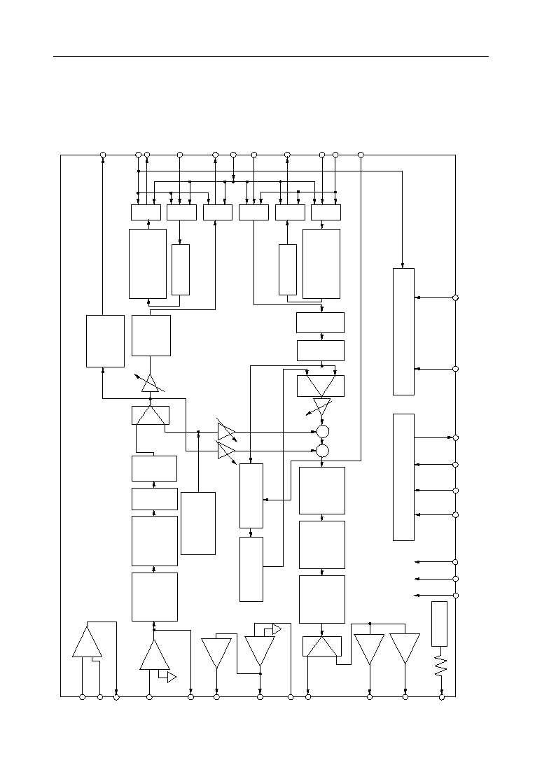
BLOCK DIAGRAM
+
≠1
+1
≠1
VOXO
XSYNC
IS
PCMSI
PCMSO
BCLK
PCMRI
PCMRO
IR
RSYNC
VOXI
ADPCM
CODER
TXMUTE
RXON/OFF
RXPAD
Ex-
pan-
der
Receive gain adjust
LPF
D/A
Conv.
RC
Filter
Clock/Timing
MCU Interface
V
REF
Voice
Detect
Compan-
der
Transmit gain adjust
Tone gain adjust
BPF
TXON/OFF
A/D
Conv.
RC
Filter
DTMF/other
Tone Generator
Noise Generator
Side tone gain adjust
AIN1≠
AIN1+
GSX1
AIN2
GSX2
AOUT+
AOUT≠
PWI
VFRO
SAO+
SAO≠
SG
VDDC
DGC
AGC
DEN
EXCK
DIN
DOUT
MCK
PDN/
RESET
RXMUTE
ADPCM
DECODER
Power Detect
P
/
S
P
/
S
P
/
S
S
/
P
S
/
P
S
/
P
≠
+
≠
+
≠
+
+
3/26
° Semiconductor
MSM7570L-01/02
PIN CONFIGURATION (TOP VIEW)
1
2
3
4
5
6
7
8
9
10
11
12
13
14
15
16
32
31
30
29
28
27
26
25
24
23
22
21
20
19
18
17
AG
SG
AIN1+
AIN1≠
GSX1
AIN2
GSX2
VFRO
PWI
AOUT≠
AOUT+
SAO+
SAO≠
PDN/RESET
VOXI
V
DD
DG
BCLK
XSYNC
RSYNC
PCMSO
PCMSI
IS
IR
PCMRO
PCMRI
MCK
DEN
EXCK
DIN
DOUT
VOXO
32-Pin Plastic TSOP
4/26
° Semiconductor
MSM7570L-01/02
PIN AND FUNCTIONAL DESCRIPTIONS
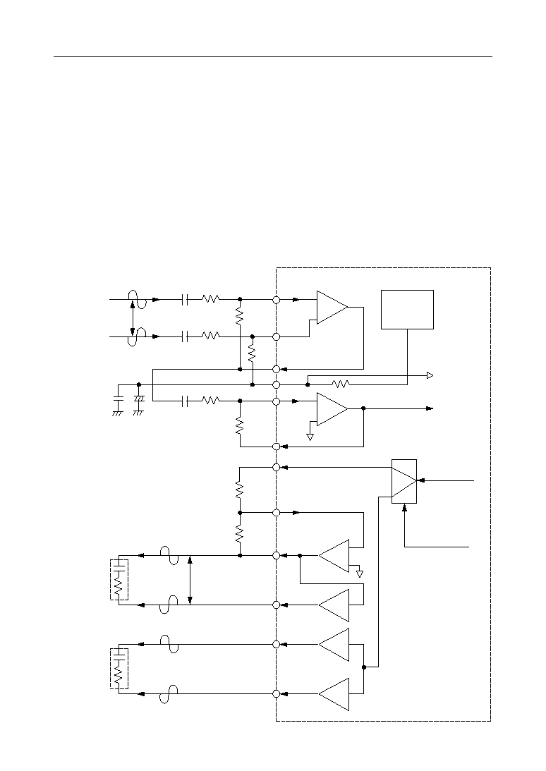
AIN1+, AIN1≠, AIN2, GSX1, GSX2
Transmits analog input and the output for transmit gain adjustment.
AIN1≠ (AIN2) connects to the inverting input of the internal transmit amplifier. AIN1+ connects
to the non-inverting input of the internal transmit amplifier. GSX1 (GSX2) connects to the
internal transmit amplifier output. Refer to Fig.1 for gain adjustment.
VFRO, AOUT+, AOUT≠, PWI
Receives analog output and the output for receive gain adjustment.
VFRO is the receive filter output. AOUT+ and AOUT≠ are differential analog signal outputs
which can directly drive Z
L
= 350 W + 120 nF or a 1.2 kW load. Refer to Fig.1 for gain adjustment.
Figure 1 Analog Input/Output Interface
Transmit Gain: V
GSX2
/Vi
= (R2/R1) • (R4/R3)
AIN1≠
GSX1
R2
C1
to ENCODER
R1
from
DECODER
Differential
Analog
Output
Receive Gain: Vo/V
FRO
= 2 • (R6/R5)
Z
L
= 120 nF
+ 350 W
AIN2
GSX2
R4
C2
R3
AOUT≠
PWI
R6
VFRO
R5
AOUT+
AIN1+
≠1
≠
+
≠
+
≠
+
C1
R1
R2
V
REF
SG
Differential
Sound Output
Z
L
= 120 nF
+ 350 W
SAO≠
≠1
SAO+
+1
SELECT
+
≠
10 mF
0.1 mF
Differential
Analog Input
Vi
V
O

5/26
° Semiconductor
MSM7570L-01/02
SAO+, SAO≠
Differential analog outputs for sound output.
Control register data CR4-B5 determines the output pins (AOUT+ and AOUT- /SAO+ and SAO-
) for the voice signal and an acoustic component of the sound tone, DTMF tone, R tone, F tone,
and various types of tones at either the VFRO pin or the SAO+ and SAO- pins. The output load
conditions of these pins are the same as those of AOUT+ and AOUT-.
SG
Analog signal ground.
The output voltage of this pin is approximately 1.4 V. Put the bypass capacitors (10
µ
F in parallel
with 0.1
µ
F ceramic type) between this pin and AG to get the specified noise characteristics.
During power-down, this output voltage is 0 V. The SG voltage if necessary should be used via
a beffer.
AG
Analog ground.
DG
Digital ground.
This ground is separated from the analog signal ground pin (AG). The DG pin must be kept as
close as possible to AG on the PCB.
V
DD
+3 V power supply.
PDN/RESET
Power down and reset control input.
A "0" level makes the IC enter a power down state. At the same time, all control register data are
reset to the initial state. Set this pin to "1" during normal operating mode. The power down state
is controlled by a logical OR with CR0-B5 of the control register. When using PDN/RESET for
power down and reset control, set CR0-B5 to digital "0".
The reset width (during "L") should be 200ns or more.
MCK
Master clock input.
The frequency must be 12.288 MHz or 19.2 MHz. The applied clock frequency is selected by the
control register data CR0-B6. The master clock signal may be asynchronous with BCLK, XSYNC,
and RSYNC.

6/26
° Semiconductor
MSM7570L-01/02
PCMSO
Transmit PCM data output.
PCM is output from MSB in synchronization with the rising edge of BCLK and XSYNC.
PCMSI
Transmit PCM data input.
This signal is converted to the transmit ADPCM data. PCM is shifted in synchronization with
the falling edge of BCLK. Normally, this pin is connected to PCMSO.
PCMRO
Receive PCM data output.
PCM is the output signal after ADPCM decoder processing. This signal is output serially from
MSB in synchronization with the rising edge of BCLK and RSYNC.
PCMRI
Receive PCM data input.
PCM is shifted on the rising edge of the BCLK and input from MSB. Normally, this pin is
connected to PCMRO.
IS
Transmit ADPCM signal output.
After having encoded PCM with ADPCM, this signal is output from MSB in synchronization
with the rising edge of BCLK and XSYNC. This pin is an open drain output and remains in a high
impedence state during power-down. IS requires a pull-up resistor.
IR
Receive ADPCM signal input.
This input signal is shifted serially on the falling edge of BCLK in synchronization with RSYNC,
and input from MSB.
BCLK
Shift clock input for the PCM data (PCMSO, PCMSI, PCMRO, PCMRI) and the ADPCM data(IS,
IR) .
The frequency is set in the 64 kHz to 2048 kHz range.

7/26
° Semiconductor
MSM7570L-01/02
XSYNC
Transmit PCM and ADPCM data 8 kHz synchronous signal input.
Synchronize this signal with BCLK signal. XSYNC is used to indicate the MSB of the transmit
serial PCM and ADPCM data stream.
Be sure to input the XSYNC signal because it is also used as the input of the timing generator.
RSYNC
Receive PCM and ADPCM data synchronous signal input.
Synchronize this signal with BCLK signal. RSYNC is used to indicate the MSB of the receive
serial PCM and ADPCM data stream.
VOXO
Transmit VOX function signal output.
VOX function voice recognizes the presence or absence of the transmit voice signal by detecting
the signal energy. "1" and "0" levels set on this pin correspond to the presence and the absence
of voice, respectively. This result appears at the register data CR7-B7. The signal energy detect
threshold is set by the control register data CR6-B6, B5.
VOXI
Signal input for receive VOX function.
A "1" level at VOXI indicates the presence of a voice signal. The decoder block processes normal
receive signal, and the voice signal appears at the analog output pins . The "0" level indicates
the absence of a voice signal. Background noise generated in this device is transferred to the
analog output pins. The background noise amplitude is set by the control register CR6. Because
this signal is ORed with the register data CR6-B3, set the control register data CR6-B3 to digital
"0".
8/26
° Semiconductor
MSM7570L-01/02
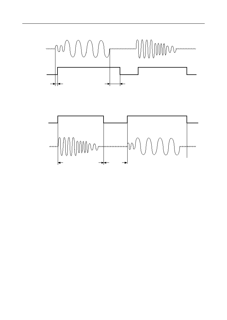
Voice Input
GSX2
VOXO
VOXI
Voice Output
VFRO
T
VXON
Voice
Detect
T
VXOFF
Silence
Detect (Hang-over time)
Normal Voice Signal
Decoded Time period
Background
Noise
(a) Transmit VOX Function Timing Diagram
(b) Receive VOX Function (CR6-B3: digital "0") Timing Diagram
Voice
Voice
Voice
Silence
Silence
Voice
Note: VOXO, VOXI functions becomes valid when setting CR6-B7 to digital "1".
Figure 2 VOX Function
9/26
° Semiconductor
MSM7570L-01/02
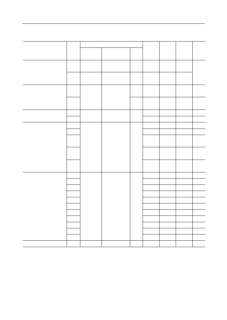
Figure 3 MCU Interface Input/Output Timing
Table 1 shows the register map.
DEN , EXCK, DIN, DOUT
Serial control ports for MCU interface.
Reading and writing data are performed by an external MCU through these pins. Eight registers
with eight bits are provided on the devices.
DEN is the "Enable" control signal input, EXCK is the data shift clock input, DIN is the address
and data input, and DOUT is the data output.
Fig.3 shows the input/output timing diagram.
R/W : Read/Write enable R : Read only register.
High Impedance
High Impedance
(a) Write Data Timing Diagram
(b) Read Data Timing Diagram
DEN
W
EXCK
DIN
A2
DOUT
A1
A0
B7
B6
B5
B4
B3
B2
B1
B0
R
A2
A1
A0
B7
B6
B5
B4
B3
B2
B1
B0
DEN
EXCK
DIN
DOUT
,
,
Table-1
Name
Address
A2
A1
A0
Control and Detect Data
R/W
B7
B6
B5
B4
B3
B2
B1
B0
CR0
0
0
0
R/W
A/m
SEL
MCK
SEL
PDN
ALL
--
--
PDN
SAO/AOUT
CR1
0
0
1
R/W
MODE1
MODE0
TX
RESET
RX
RESET
TX
MUTE
RX
MUTE
--
RX
PAD
CR2
0
1
0
R/W
TX
ON/OFF
TX
GAIN2
TX
GAIN1
TX
GAIN0
RX
ON/OFF
RX
GAIN2
RX
GAIN1
RX
GAIN0
CR3
0
1
1
R/W
Side Tone
GAIN2
Side Tone
GAIN1
Side Tone
GAIN0
TONE
ON/OFF
TONE
GAIN3
TONE
GAIN2
TONE
GAIN1
TONE
GAIN0
CR4
1
0
0
R/W
DTMF/
OTHERS
SEL
TONE
SEND
SAO/
VFRO
TONE4
TONE3
TONE2
TONE1
TONE0
CR5
1
0
1
R/W
--
--
--
--
--
--
--
--
CR6
1
1
0
R/W
VOX
ON/OFF
ON
LVL1
ON
LVL0
OFF
TIME
VOX
IN
RX NOISE
LEVEL SEL
RX NOISE
LVL1
RX NOISE
LVL0
CR7
1
1
1
R
VOX
OUT
TX NOISE
LVL1
TX NOISE
LVL0
--
--
--
--
--
--
--
10/26
° Semiconductor
MSM7570L-01/02
ABSOLUTE MAXIMUM RATINGS
Parameter
Power Supply Voltage
Analog Input Voltage
Digital Input Voltage
Storage Temperature
Symbol
V
DD
V
AIN
V
DIN
T
STG
Condition
--
--
--
--
Rating
≠0.3 to +5
≠ 0.3 to V
DD
+ 0.3
≠0.3 to V
DD
+ 0.3
≠55 to +150
Unit
V
V
V
∞C
RECOMMENDED OPERATING CONDITIONS
Parameter
Symbol
Condition
Min.
Typ.
Max.
Unit
Power Supply Voltage
V
DD
Voltage must be fixed
2.7
--
3.6
V
MCK, XSYNC, RSYNC, PCMRI,
PCMSI, BCLK, IR, PDN/RESET,
DEN, EXCK, DIN
Digital Input High Voltage
V
IH
0.45
•
V
DD
--
V
DD
V
MCK, XSYNC, RSYNC, PCMRI,
PCMSI, BCLK, IR, PDN/RESET,
DEN, EXCK, DIN
Digital Input Low Voltage
V
IL
0
--
0.16
•
V
DD
V
Master Clock Frequency
f
MCK1
MCK (CR0≠B6 = "0")
≠0.01%
12.288
+0.01%
MHz
Bit Clock Frequency
f
BCK
BCLK
64
--
2048
kHz
Synchronous Signal Frequency
f
SYMC
XSYNC, RSYNC
--
8.0
--
kHz
Clock Duty Ratio
D
C
MCK, BCLK, EXCK
30
50
70
%
MCK, XSYNC, RSYNC, PCMRI,
PCMSI, BCLK, IR, PDN/RESET,
DEN, EXCK, DIN
Digital Input Rise Time
t
Ir
--
--
50
ns
MCK, XSYNC, RSYNC, PCMRI,
PCMSI, BCLK, IR, PDN/RESET,
DEN, EXCK, DIN
Digital Input Fall Time
t
If
--
--
50
ns
Transmit Sync Signal Setting Time
t
XS
BCLK to XSYNC
100
--
--
ns
t
XS
XSYNC to BCLK
100
--
--
ns
Receive Sync Signal Setting Time
t
RS
BCLK to RSYNC
100
--
--
ns
t
SR
RSYNC to BCLK
100
--
--
ns
Synchronous Signal Width
t
WS
XSYNC, RSYNC
1 BCLK
--
100
m
s
Bypass Capacitors for SG
C
SG
10 + 0.1
--
--
m
F
Digital Output Load
R
DL
IS (Pull-up Resistor)
500
--
--
W
C
DL
--
--
100
pF
IS, PCMSO, PCMRO, VOXO, DOUT
Operating Temperature
Ta
--
≠25
+25
+70
∞C
f
MCK2
MCK (CR0≠B6 = "1")
≠0.01%
19.200
+0.01%
MHz
PCM, ADPCM Set-up Time
t
DS
100
--
--
ns
PCM, ADPCM Hold Time
t
DH
100
--
--
ns
--
--
SG to AG
11/26
° Semiconductor
MSM7570L-01/02
Parameter
Power Supply Current
Input High Voltage
Input Low Voltage
Output Low Voltage
Output Leakage Current
Input Capacitance
Symbol
I
DD1
I
DD2
V
IH
V
IL
V
OL
I
O
Condition
Operating Mode,
No Signal, (V
DD
= 3.0 V)
Power Down Mode, (V
DD
= 3.0 V)
--
--
1 LSTTL, Pull-up: 500 W
IS
Min.
--
--
0.45
0.0
0.0
--
Typ.
7
0.1
--
--
0.2
--
Max.
14
0.2
V
DD
0.16
0.4
10
Unit
mA
mA
V
V
V
m
A
C
IN
--
--
5
--
pF
(V
DD
=
2.7 V to 3.6 V, Ta = ≠25∞C to +70∞C)
Output Resistance
R
OSG
SG
--
25
50
kW
•
V
DD
•
V
DD
Input Leakage Current
I
IH
I
IL
V
I
=
V
DD
V
I
=
0 V
--
--
--
--
2.0
0.5
m
A
m
A
SG Warm-up Time
T
SG
SG¥GND 10 + 0.1 mF
(Rise time to 90% of max. level)
--
700
--
ns
ELECTRICAL CHARACTERISTICS
DC and Digital Interface Characteristics
Parameter
Input Resistance
Output Load Resistance
Output Load Capacitance
Output Amplitude
Input Offset Voltage
Symbol
R
INX
R
LGX
C
LGX
V
OGX
V
OFGX
Condition
AIN1+ , AIN1≠ , AIN2
Min.
10
20
--
--
≠20
Typ.
--
--
--
--
--
Max.
--
--
100
*1.30
+20
Unit
MW
kW
pF
V
PP
mV
GSX1, GSX2
GSX1, GSX2
GSX1, GSX2, R
L
= 20 kW
Pre≠OPAMPs
(V
DD
=
2.7 V to 3.6 V, Ta = ≠25∞C to +70∞C)
Transmit Analog Interface Characteristics
*
≠7.7 dBm (600 W) = 0 dBm0, + 3.14 dBm0 = 1.30 V
PP
(A-law)
≠7.7 dBm (600 W) = 0 dBm0, + 3.17 dBm0 = 1.30 V
PP
(m-law)
12/26
° Semiconductor
MSM7570L-01/02
Parameter
Input Resistance
Output Load Resistance
Output Capacitance
Symbol
R
INPW
R
LVF
R
LAO
C
LVF
C
LAO
Condition
PWI
Min.
10
20
1.2
--
--
Typ.
--
--
--
--
--
Max.
--
--
--
100
100
Unit
MW
kW
kW
pF
pF
VFRO
Output Voltage Level
Offset Voltage
V
OVF
V
OAO
V
OFVF
V
OFAO
--
--
≠100
≠20
--
--
--
--
*1.30
+100
+20
V
PP
V
PP
mV
mV
VFRO,
AOUT+, AOUT≠, SAO+, SAO≠
VFRO
AOUT+, AOUT≠, SAO+, SAO≠
AOUT+,
AOUT≠,
SAO+,
SAO≠
VFRO
AOUT+, AOUT≠ (GAIN = 0 dB,
Power amp only) SAO+, SAO≠
G
DB
40
--
--
dB
Power amp (0.3 to 3.4 kHz,
Z
L
= 350 W + 120 nF)(See Fig.1)
R
L
= 20 kW
Z
L
= 350 W
+ 120 nF(See Fig.1)
R
L
= 1.2 kW
--
--
V
PP
(V
DD
=
2.7 V to 3.6 V, Ta = ≠25∞C to +70∞C)
*1.30
*1.30
Open Loop Gain
*
≠7.7 dBm (600 W) = 0 dBm0, + 3.14 dBm0 = 1.30 V
PP
(A-law)
≠7.7 dBm (600 W) = 0 dBm0, + 3.17 dBm0 = 1.30 V
PP
(m-law)
Receive Analog Interface Characteristics
13/26
° Semiconductor
MSM7570L-01/02
Parameter
Transmit Frequency
Response
Symbol
L
OSS
T1
Level
0 to 60
Min.
25
Typ.
--
Max.
--
Unit
dB
Freq.
Others
L
OSS
T2 300 to 3000
≠0.15
--
+0.20
dB
L
OSS
T3
1020
Reference
dB
0
L
OSS
T4
3300
≠0.15
--
+0.80
dB
L
OSS
T5
3400
0
--
0.80
dB
L
OSS
T6
3968.75
13
--
--
dB
Receive Frequency
Response
0 to 3000
≠0.15
--
+0.20
dB
1020
Reference
dB
3300
≠0.15
--
+0.80
dB
0
3400
0
--
0.80
dB
3968.75
13
--
--
dB
Transmit Signal
to Distortion Ratio
SD T1
35
--
3
SD T2
35
--
0
SD T3
35
--
≠30
SD T4
1020
28
--
≠40
SD T5
23
--
≠45
Receive Signal
to Distortion Ratio
SD R1
--
3
SD R2
--
0
SD R3
--
≠30
SD R4
1020
--
≠40
SD R5
--
≠45
Transmit Gain
Tracking
GT T1
≠0.2
+0.2
GT T2
Reference
GT T3
1020
≠0.2
+0.2
≠40
GT T4
≠0.5
+0.5
GT T5
≠1.2
+1.2
3
≠10
≠50
≠55
Receive Gain
Tracking
GT R1
≠0.2
+0.2
GT R2
Reference
GT R3
1020
≠0.2
+0.2
GT R4
≠0.5
+0.5
GT R5
≠1.2
+1.2
≠40
3
≠10
≠50
≠55
Condition
L
OSS
R1
L
OSS
R2
L
OSS
R3
L
OSS
R4
L
OSS
R5
35
35
35
28
23
--
--
--
--
--
--
--
--
--
--
--
--
--
--
--
--
--
--
(*1)
(*1)
--
--
--
--
dB
dB
dB
dB
dB
dB
dB
dB
dB
dB
dB
dB
dB
dB
dB
dB
dB
dB
dB
dB
(V
DD
=
2.7 V to 3.6 V, Ta = ≠25∞C to +70∞C)
(dBm0)
(Hz)
AC Chracteristics
*1 Use the P-message weighted filter
14/26
° Semiconductor
MSM7570L-01/02
Digital Output
Delay Time
PCM and ADPCM
Interface
t
SDX
0
--
200
t
SDR
0
--
200
t
XD1
0
--
200
t
XD2
0
--
200
ns
1 LSTTL + 100 pF,
Pull-up: 500 W
P
SRRT
Noise Freq.
: 0 to 50 kHz
30
--
--
dB
Power Supply Noise
Rejection Ratio
Noise Level
: 50 mV
PP
--
P
SRRR
t
XD3
0
--
200
Parameter
Symbol
Level
Min.
Typ.
Max.
Unit
(V
DD
=
2.7 V to 3.6 V, Ta = ≠25∞C to +70∞C)
Freq.
Others
Condition
--
See
Fig.4
30
--
--
dB
ns
ns
ns
ns
t
RD1
t
RD2
t
RD3
t
M1
50
--
--
ns
t
M2
50
--
--
ns
t
M3
50
--
--
ns
t
M4
50
--
--
ns
t
M5
100
--
--
ns
t
M6
50
--
--
ns
t
M7
50
--
--
ns
t
M8
0
--
50
ns
t
M9
50
--
--
ns
t
M10
50
--
--
ns
t
M11
0
--
50
ns
Serial Port Digital
Input/Output Setting
Time
C
L
= 100 pF
--
See
Fig.5
f
EXCK
--
--
10
MHz
--
--
EXCK
Shift Clock Frequency
(dBm0)
(Hz)
N
IDLT
--
--
--
≠68
(≠75.7) dBmOp
(dBmp)
N
IDLR
--
--
1020
A
VT
0.285
0.320
(*3)
0.359
0
A
VR
0.285
0.320
(*3)
0.359
--
≠72
(≠79.7)
Idle Channel Noise
AIN = SG
(*1)
(*2)
Vrms
Vrms
GSX2
Absolute Signal
Amplitude
VFRO
(*1)
--
AC Characteristics (Continued)
*1 Use the P-message weighted filter
*2 PCMRI input code
"11010101"(A-law)
"11111111"(m-law)
*3 0.320 Vrms = 0 dBm0 = ≠7.7 dBm
Note: All ADPCM coder and decoder characteristics comply with ITU-T Recommendation
G.726.
15/26
° Semiconductor
MSM7570L-01/02
≠2.5
dB
t
VXON
OFF ∆ ON
--
10
--
ms
Transmit VOX Detect Time
(Voice Signal ON/OFF Detect Time
)
t
VXOF
Parameter
Symbol
Min.
Typ.
Max.
Unit
(V
DD
=
2.7 V to 3.6 V, Ta = ≠25∞C to +70∞C)
Condition
150/310 160/320 170/330
ms
ON ∆ OFF
D
VX
To the values (CR6-B6, B5)
VOXO,
See Fig.2
0
+2.5
Transmit VOX Detect Level
Accuracy
(Threshold Level)
*5
≠18
≠16
≠10
≠8
dBm0
D
FT1
DTMF Tones
≠7
--
+7
Hz
Frequency Difference
D
FT2
Parameter
Symbol
Min.
Typ.
Max.
Unit
(V
DD
=
2.7 V to 3.6 V, Ta = ≠25∞C to +70∞C)
Condition
≠7
--
+7
Hz
dBm0
dBm0
dBm0
Other Tones
V
TL
Transmit Tones
(Gain setting 0dB)
V
TH
V
RL
V
RH
1
dBm0
R
DTMF
V
TH
/V
TL
, V
RH
/V
RL
Original (reference)
Tone Signal Level
*4
Relative Level of
DTMF Tones
DTMF (High)
and Other Tones
DTMF (Low)
DTMF (High)
and Other Tones
≠16
≠14
≠8
≠6
2
≠14
≠12
≠6
≠4
3
Receive Tones
(Tone generator
gain setting ≠6dB)
DTMF (Low)
AC Characteristics (DTMF and Other Tones)
*4 Does not contain the setting value set for the programmable gain
AC Characteristics (Programmable Gain Stages)
D
G
All gain stages, to programmed value
≠1
0
+1
dB
Gain Accuracy
Parameter
Symbol
Min.
Typ.
Max.
Unit
(V
DD
=
2.7 V to 3.6 V, Ta = ≠25∞C to +70∞C)
Condition
AC Characteristics (VOX Function)
*5 When single tone is input at 1000Hz
16/26
° Semiconductor
MSM7570L-01/02
1
2
3
4
5
6
7
8
9
10
1
2
3
4
5
6
7
8
9
10
0
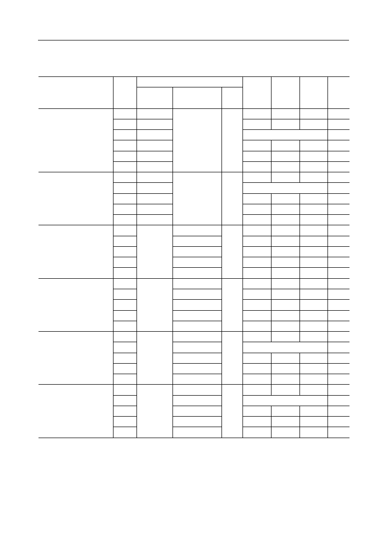
t
XD1
t
XD2
t
WS
t
SX
t
XS
t
SDX
MSB
LSB
t
XS
t
SX
t
XD1
t
XD2
MSB
LSB
t
XD3
t
XD3
t
SDX
BCLK
XSYNC
PCMSO
BCLK
XSYNC
IS
0
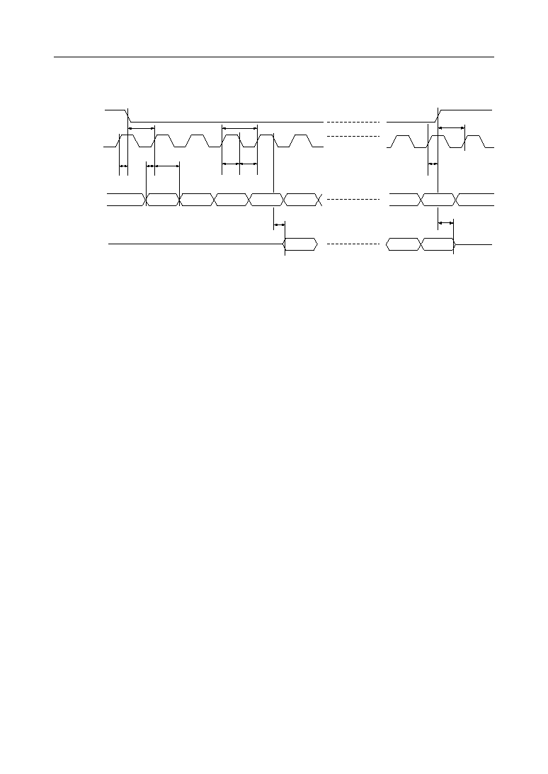
TIMING DIAGRAM
Transmit Side PCM/ADPCM Data Interface
Figure 4 PCM/ADPCM Data Interface
1
2
3
4
5
6
7
8
9
10
1
2
3
4
5
6
7
8
9
10
0
t
RD1
t
RD2
t
WS
t
SR
t
RS
t
SDR
MSB
LSB
t
RS
t
SR
t
RD3
BCLK
RSYNC
PCMRO
BCLK
RSYNC
MSB
LSB
IR
t
DH
t
DS
0
Receive Side PCM/ADPCM Data Interface
17/26
° Semiconductor
MSM7570L-01/02
Figure 5 MCU Interface
Serial Port Data Transfer for MCU Interface
t
M1
t
M3
t
M4
t
M2
1
2
3
4
5
6
t
M6
t
M7
t
M5
11
12
t
M10
t
M11
W/R
A2
A1
A0
B7
B7
t
M8
B1
B0
B1
B0
t
M9
DEN
EXCK
DIN
DOUT

18/26
° Semiconductor
MSM7570L-01/02
FUNCTIONAL DESCRIPTION
Control Registers
(1) CR0 (Basic operating mode)
Note: Initial Value: Reset state by PDN/RESET
B7 ...PCM Companding law select;
0/
µ
-law, 1/A-law
B6 ...Master clock frequency select;
0/12.288 MHz, 1/19.200 MHz
B5 ...Power down (entire system);
0/Power on, 1/Power down
When using this data for power down control, set pin PDN/RESET at "1"level.
The control registers are not reset by this signal.
B2 ...Not used
B1 ...Not used
B0 ...Power Down for Sound output amps: (SAO+, SAO≠), or Receiver output amp (AOUT+,
AOUT≠, VFRO );
If this data is set to digital "1", either a pair of sound amplifiers or a pair of reciver
amplifiers enters the power down state depending on the set data on CR4-B5.
If this data is set to digital "0", sound amplifiers and receiver amplifiers are in the power-
on state.
B4, B3 ... Not used (These pins are used to test the device. They should be set to "0" during normal
operation.)
B0
PDN
SAO/AOUT
0
B1
--
0
B2
--
0
B3
--
0
B4
--
0
B5
PDN ALL
0
B6
MCK SEL
0
B7
A/m SEL
0
CR0
Initial Value (Note)

19/26
° Semiconductor
MSM7570L-01/02
(2) CR1 (ADPCM block operating mode)
B7, B6 ... ADPCM data compression algorithm select;
(0, 0):
32 kbps
(0, 1):
64 kbps (data through)
(1, 0):
24 kbps
(1, 1):
16 kbps
B5 ... ADPCM of transmit reset (specified by G.726);
1/Reset*
B4 ... ADPCM of receive reset (specified by G.726 );
1/Reset*
B3 ... ADPCM transmit data mute,
1/Mute
B2 ... ADPCM receive data mute,
1/Mute
B1 ... Not used
B0 ... Receive side PAD,
1/inserted,12 dB loss
0/no PAD
*
The reset width should be 125ms or more.
The transmitter and receiver cannot be reset separately.
They must be reset at the same time.
B0
RX PAD
0
B1
--
0
B2
RX MUTE
0
B3
TX MUTE
0
B4
RX RESET
0
B5
TX RESET
0
B6
MODE0
0
B7
MODE1
0
CR1
Initial Value

20/26
° Semiconductor
MSM7570L-01/02
This programmable gain table, not only for transmit/receive voice signal and the transmitted
DTMF and other tones. The transmission of these tone signal is enabled by the CR4-B6 data
described later. The original (reference) signal amplitude of these tones is analogically defined
as follows.
DTMF low-group-tones .................................... ≠16 dBm0
DTMF high-group-tones and others............... ≠14 dBm0
For example, when selecting +8 dB (B6, B5, B4) = (1,1,1) as a transmit gain, each tone signal
amplitude with an analogical expression on the pin PCMSO becomes as follows .
DTMF low-group tones .................................... ≠8 dBm0
DTMF high-group tones and other tones ...... ≠6 dBm0
Gain setting for the side tone (path to receive side from transmit side) and the receive side tone
is performed by register CR3.
(3) CR2 (PCM CODEC operational mode setting and transmit/receive gain adjustment)
B7 ... PCM Coder disable;
0/Enable, 1/Disable (transmit PCM idle pattern)
B6, B5, B4 ... Transmit gain adjustment, refer to Table-2.
B3 ... PCM Decoder disable;
0/Enable, 1/Disable (receive PCM idle pattern)
B2, B1, B0 ... Receive gain setting, refer to Table-2.
Table-2
B0
RX GAIN0
0
B1
RX GAIN1
0
B2
RX GAIN2
0
B3
RX ON/OFF
0
B4
TX GAIN0
0
B5
TX GAIN1
0
B6
TX GAIN2
0
B7
TX ON/OFF
0
CR2
Initial Value
B6
B5
B4
Transmit Gain
B2
B1
B0
Receive Gain
0
0
0
≠6 dB
0
0
0
≠6 dB
0
0
1
≠4 dB
0
0
1
0
1
0
≠2 dB
0
1
0
0
1
1
0 dB
0
1
1
1
0
0
+2 dB
1
0
0
1
0
1
+4 dB
1
0
1
1
1
0
+6 dB
1
1
0
1
1
1
+8 dB
1
1
1
≠4 dB
≠2 dB
0 dB
+2 dB
+4 dB
+6 dB
+8 dB
21/26
° Semiconductor
MSM7570L-01/02
(4) CR3 (Side tone and other tone generator gain setting)
The tone generator gain setting table for the receive side, as shown in Table-4, depends upon the
following reference level.
DTMF low-group tones ................................ ≠2 dBm0
DTMF high-group tones and others ............ 0 dBm0
For example, when selecting ≠6 dB (B3, B2, B1, B0) = (1, 1, 1, 1) as a tone generator gain, each DTMF
tone signal amplitude on SAO+/SAO≠ or VFRO is as follows.
DTMF low-group tone .................................. ≠8 dBm0
DTMF high-group tone or other tones ....... ≠6 dBm0
B7, B6, B5 ... Side tone path gain setting, refer to Table-3.
B4 ... Tone generator enable;
0/Disable, 1/Enable
B3, B2, B1, B0 ... Tone generator gain adjustment for receive side, refer to Table-4
Table-3
B7
B6
B5
Side Tone Path Gain
0
0
0
OFF
0
0
1
≠21 dB
0
1
0
0
1
1
1
0
0
1
0
1
1
1
0
1
1
1
≠19 dB
≠17 dB
≠15 dB
≠13 dB
≠11 dB
≠9 dB
Table-4
B0
TONE
GAIN0
0
B1
TONE
GAIN1
B2
TONE
GAIN2
B3
TONE
GAIN3
B4
TONE
ON/OFF
B5
Side. Tone
GAIN0
B6
Side. Tone
GAIN1
B7
Side. Tone
GAIN2
0
0
0
0
0
0
0
CR3
Initial Value
B3
B2
B1
B0
Tone Generator Gain
B3
B2
B1
B0
Tone Generator Gain
0
0
0
0
≠36 dB
1
0
0
0
≠20 dB
0
0
0
1
≠34 dB
1
0
0
1
≠18 dB
0
0
1
0
≠32 dB
1
0
1
0
≠16 dB
0
0
1
1
≠30 dB
1
0
1
1
≠14 dB
0
1
0
0
≠28 dB
1
1
0
0
≠12 dB
0
1
0
1
≠26 dB
1
1
0
1
≠10 dB
0
1
1
0
≠24 dB
1
1
1
0
≠8 dB
0
1
1
1
≠22 dB
1
1
1
1
≠6 dB
22/26
° Semiconductor
MSM7570L-01/02
(5) CR4 (Tone genereator operating mode and frequency select)
(b) B7 = 0 (Other tones)
<MSM7570L-01>
B7 ... DTMF or other tones select; 0/Others, 1/DTMF
B6 ... Tone transmit enable (Transmit side); 0/Voice signal (transmit), 1/Tone transmit
B5 ... Tone output pin select (Receive side); 0/VFRO, 1/SAO+ and SAO≠
B4, B3, B2, B1, B0 ... Tone frequency setting, referred to Table-5-1, 5-2, and 5-3.
(a) B7 = 1 (DTMF tone)
*Unrelated
Table-5-1
Table-5-2
B0
B1
B2
B3
B4
B5
B6
B7
TONE0
TONE1
TONE2
TONE3
TONE4
SAO/
VFRO
TONE
SEND
DTMF/OTHERS
SEL
0
0
0
0
0
0
0
0
CR4
Initial Value
B4
B3
B2
B1
B0
Frequency
B4
B3
B2
B1
B0
Frequency
*
0
0
0
0
697 Hz + 1209 Hz
*
1
0
0
0
852 Hz + 1209 Hz
0
0
0
1
697 Hz + 1336 Hz
1
0
0
1
852 Hz + 1336 Hz
0
0
1
0
697 Hz + 1477 Hz
1
0
1
0
852 Hz + 1477 Hz
0
0
1
1
697 Hz + 1633 Hz
1
0
1
1
852 Hz + 1633 Hz
0
1
0
0
770 Hz + 1209 Hz
1
1
0
0
941 Hz + 1209 Hz
0
1
0
1
770 Hz + 1336 Hz
1
1
0
1
941 Hz + 1336 Hz
0
1
1
0
770 Hz + 1477 Hz
1
1
1
0
941 Hz + 1477 Hz
0
1
1
1
1
1
1
1
*
*
*
*
*
*
*
*
*
*
*
*
*
*
770 Hz + 1633 Hz
941 Hz + 1633 Hz
B4
B3
B2
B1
B0
Frequency
B4
B3
B2
B1
B0
Frequency
0
0
0
0
0
1k/1333 Hz, 16 Hz wamb.
1
0
0
0
0
2000 Hz Single tone
0
0
0
0
1
800/667 Hz, 16 Hz wamb.
1
0
0
0
1
2042 Hz Single tone
0
0
0
1
0
800/1k Hz,16 Hz wamb.
1
0
0
1
0
2514 Hz Single tone
0
0
0
1
1
500/667 Hz,16 Hz wamb.
1
0
0
1
1
500 Hz Single tone
0
0
1
0
0
500/400 Hz,16 Hz wamb.
1
0
1
0
0
667 Hz Single tone
0
0
1
0
1
800/1k Hz, 8 Hz wamb.
1
0
1
0
1
1333 Hz Single tone
0
0
1
1
0
500/400 Hz, 8 Hz wamb.
1
0
1
1
0
2100 Hz Single tone
0
0
1
1
1
400 Hz,16 Hz wamb.
1
0
1
1
1
--
0
1
0
0
0
400 Hz,20 Hz wamb.
1
1
0
0
0
--
0
1
0
0
1
400 Hz Single tone
1
1
0
0
1
--
0
1
0
1
0
425 Hz Single tone
1
1
0
1
0
0
1
0
1
1
440 Hz Single tone
1
1
0
1
1
0
1
1
0
0
450 Hz Single tone
1
1
1
0
0
0
1
1
0
1
800 Hz Single tone
1
1
1
0
1
0
1
1
1
0
1000 Hz Single tone
1
1
1
1
0
0
1
1
1
1
1300 Hz Single tone
1
1
1
1
1
--
--
--
--
--
--
23/26
° Semiconductor
MSM7570L-01/02
(b) B7 = 0 (Other tones)
<MSM7570L-02>
Table-5-3
(6) CR5 (Not used)
B7 ≠ B0..... Not used
B4
B3
B2
B1
B0
Frequency
B4
B3
B2
B1
B0
Frequency
0
0
0
0
0
1k/1333 Hz 16 Hz wamb.
1
0
0
0
0
2500 Hz Single tone
0
0
0
0
1
800/1k Hz 16 Hz wamb.
1
0
0
0
1
2600 Hz Single tone
0
0
0
1
0
800/1k Hz 8 Hz wamb.
1
0
0
1
0
2670 Hz Single tone
0
0
0
1
1
400 Hz, 16 Hz wamb.
1
0
0
1
1
2700 Hz Single tone
0
0
1
0
0
2700 Hz, 16 Hz wamb.
1
0
1
0
0
2800 Hz Single tone
0
0
1
0
1
400 Hz
1
0
1
0
1
2910 Hz Single tone
0
0
1
1
0
800 Hz
1
0
1
1
0
3000 Hz Single tone
0
0
1
1
1
1000 Hz
1
0
1
1
1
3110 Hz Single tone
0
1
0
0
0
1333 Hz
1
1
0
0
0
3200 Hz Single tone
0
1
0
0
1
1440 Hz
1
1
0
0
1
--
0
1
0
1
0
1900 Hz
1
1
0
1
0
0
1
0
1
1
2000 Hz
1
1
0
1
1
0
1
1
0
0
2100 Hz
1
1
1
0
0
0
1
1
0
1
2180 Hz
1
1
1
0
1
0
1
1
1
0
2300 Hz
1
1
1
1
0
0
1
1
1
1
2400 Hz
1
1
1
1
1
--
--
--
--
--
--
B0
B1
B2
B3
B4
B5
B6
B7
--
0
--
0
--
0
--
0
--
0
--
0
--
0
--
0
CR5
Initial Value
24/26
° Semiconductor
MSM7570L-01/02
(7) CR6 (VOX function control)
B7 ... VOX function enable;
0/Disable, 1/Enable
B6, B5 ... Transmit signal energy detect (Transmit VOX) threshold
(0, 0): ≠30 dBm0
(0, 1): ≠35 dBm0
(1, 0): ≠40 dBm0
(1, 1): ≠45 dBm0
B4 ... Hang-over time (Fig.2, T
VXOFF)
;
0/160 ms, 1/320 ms
B3 ... Receive VOX function setting;
0/Background noise transmit, 1/Voice signal detect
When using this data for control, set pin VOXI at "0" level.
B2 ... Background noise amplitude setting;
0/Automatic, 1/Programmable by B1 and B0
Automatic : Set the noise at the voice signal amplitude when B3 (or VOXI) changes from
"1" to digital "0".
B1, B0 ... (0, 0): No noise
(0, 1): ≠55 dBm0
(1, 0): ≠45 dBm0
(1, 1): ≠35 dBm0
(8) CR7 (Detect register, read only)
*
For IC test
B7 ... Transmit VOX function result;
0/Silence, 1/Voice
B6, B5 ... Transmit silence level (indicator); (at 1000 Hz)
(0, 0) : Below ≠60 dBm0
Note: These outputs are valid only when the VOX
(0, 1) : ≠50 to ≠60 dBm0
function is enabled by CR6-B7.
(1, 0) : ≠40 to ≠50 dBm0
(1, 1) : Above ≠40 dBm0
B4 ... Not used
B3 ... Not used
B2 ... Not used
B1 ... Not used
B0 ... Not used
B0
RX NOISE
LVL0
0
B1
RX NOISE
LVL1
0
B2
RX NOISE
LEVEL SEL
0
B3
VOX IN
0
B4
OFF
TIME
0
B5
ON
LVL0
0
B6
ON
LVL1
0
B7
VOX
ON/OFF
0
CR6
Initial Value
B0
B1
B2
B3
--
B4
*
B5
TX NOISE
LVL0
0
B6
TX NOISE
LVL1
0
B7
VOX
OUT
0
CR7
Initial Value
--
*
--
*
--
*
*
--
25/26
° Semiconductor
MSM7570L-01/02
* Single-ended Analog Input Stage Type
1
2
3
4
5
6
7
8
9
10
11
12
13
14
15
16
32
31
30
29
28
27
26
25
24
23
22
21
20
19
18
17
MSM7570L-01/02 TS
AG
AIN1+
AIN1≠
GSX1
AIN2
GSX2
VFRO
PWI
AOUT≠
AOUT+
SAO+
SAO≠
PDN/RESET
VOXI
V
DD
DG
BCLK
XSYNC
RSYNC
PCMSO
PCMSI
IS
IR
PCMRO
PCMRI
MCK
DEN
EXCK
DIN
DOUT
VOXO
V
DD
8 kHz Sync. Signal input
Bit Clock
(64 kHz to 2048 kHz)
ADPCM Output
ADPCM Input
VOX OUT
Interface
Serial MCU
Master Clock
Power-Down/Reset Input
Receive Voice Analog Output
VOX IN
+
≠
SG
Transmit
Voice
Analog Input
V
DD
Sound
+
≠
APPLICATION CIRCUIT
26/26
° Semiconductor
MSM7570L-01/02
(Unit : mm)
PACKAGE DIMENSIONS
Notes for Mounting the Surface Mount Type Package
The SOP, QFP, TSOP, SOJ, QFJ (PLCC), SHP and BGA are surface mount type packages, which
are very susceptible to heat in reflow mounting and humidity absorbed in storage.
Therefore, before you perform reflow mounting, contact Oki's responsible sales person for the
product name, package name, pin number, package code and desired mounting conditions
(reflow method, temperature and times).
TSOPI32-P-814-0.50-1K
Package material
Lead frame material
Pin treatment
Solder plate thickness
Package weight (g)
Epoxy resin
42 alloy
Solder plating
5 mm or more
0.27 TYP.
Mirror finish