MSM7577
° Semiconductor
1/8
GENERAL DESCRIPTION
The MSM7577 is an LSI for Audio Signal Level adjustment for telephone set, etc.
Conventionally, its circuit has been made within individual unit, such as amplifiers, resistors and
switches. However, using this LSI allows for simple mounting and economically small space.
FEATURES
Receiving system
∑
∑
∑
∑
∑ Built-in electrical volume
Digital control (3 bit / 8 step)
∑
∑
∑
∑
∑ For transmission voice, with side tone route available.
∑
∑
∑
∑
∑ Mute function available.
Transmitting system
∑
∑
∑
∑
∑ Built-in operational amplifier for transmission signal level adjustment.
∑
∑
∑
∑
∑ Mute function available.
∑
∑
∑
∑
∑ Single +2.7 V to +5.25 V power supply
∑
∑
∑
∑
∑ Power down function
∑
∑
∑
∑
∑ Package:
16-pin plastic SOP
(SOP16-P-300-1.27-K) (Product name : MSM7577MS-K)
APPLICATION
Cellular handset, cordless telephone, etc.
° Semiconductor
MSM7577
Voice Signal Level Control LSI
E2A0045-16-X1
This version: Jan. 1998
Previous version: Nov. 1996
MSM7577
° Semiconductor
3/8
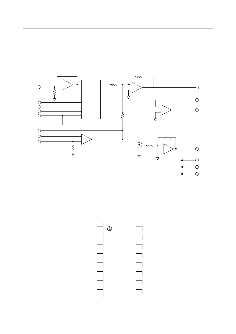
PIN DESCRIPTION
Pin No.
Name
I/O
Description
1
TAUD
O
Output pin of transmitting voice.
2
AN2
I
Receive voice input.
Gain control should be connected by a resistor between AN2 pin RCV2 pin.
4
RCV2
O
Output pin of receiving voice.
Gain control should be connected by a resistor between AN2 and RCV2 pin.
RCV2 signal is opposite phase to RCV1 signal.
6
NC
--
No Connection.
7
RAUD
I
Receive voice input.
8
GND
--
Ground (0 V).
9
10
11
ATT0
ATT1
ATT2
I
Volume control.
ATT2
ATT1
ATT0
Loss level (dB)
0
0
0
0 ±0.3
0
0
1
≠2 ±0.3
0
1
0
≠4 ±0.3
0
1
1
≠7 ±0.3
1
0
0
≠10 ±0.3
1
0
1
≠13 ±0.3
1
1
0
≠16 ±0.3
1
1
1
≠19 ±0.3
12
ATTE
I
Mute signal input.
H : Mute mode
L : Operating mode
13
AN3
I
Gain control and frequency responce control.
Gain control should be controlled by a resistor between AN3 and AO3.
14
MIC
I
Input pin of Microphone signal.
15
AO3
O
Gain control and frequency responce control.
Gain control should be controlled by a resistor between AN3 and AO3.
16
V
DD
--
Power supply (+3 V).
3
PD
1
Power down control.
H : Power down
L : Power on
5
RCV1
O
Receive voice input.
RCV1 signal is opposite phase to RCV2 signal.

MSM7577
° Semiconductor
4/8
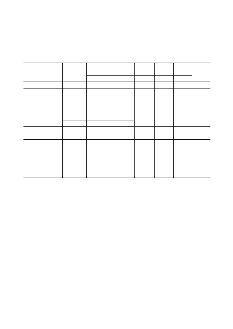
ABSOLUTE MAXIMUM RATINGS
RECOMMENDED OPERATING CONDITIONS
Parameter
Symbol
Min.
Max.
Unit
Power Supply Voltage
V
DD
≠0.3
+7.0
V
Digital Input Voltage
V
IND
≠0.3
V
DD
+ 0.3
V
Analog Input Voltage
V
INA
≠0.3
V
DD
+ 0.3
V
Storage Temperature
T
STG
≠55
+150
∞C
Parameter
Symbol
Min.
Typ.
Max.
Unit
Condition
Operating Temperature
Ta
≠20
25
70
∞C
--
Power Supply Voltage
V
DD
+2.7
+3.00
+5.25
V
V
DD
Analog Output Load
Resistance 1
R
LA1
600
--
--
W
TAUD
Analog Output Load
Resistance 2
R
LA2
10
--
--
kW
Except TAUD pin.
MSM7577
° Semiconductor
5/8
ELECTRICAL CHARACTERISTICS
DC Characteristics
Parameter
Symbol
Condition
Min.
Typ.
Max.
Unit
Power Supply Current
I
DD
--
1.2
2.4
mA
V
DD
= 3.0 V
Low Level Input
Voltage
V
IL
0
--
0.3 •
VDD
V
ATT0 to ATT2
ATTE, PD
High Level Input
Voltage
V
IH
0.7 •
VDD
--
V
DD
V
ATT0 to ATT2
ATTE, PD
Digital Input Leakage
Current
I
IL
≠10
--
+10
mA
V
I
= GND
I
IH
V
I
= V
DD
Analog Input
Voltage Level
V
IA
--
--
1.2
V
P-P
RAUD, MIC
AN2, AN3
Analog Input
Resistance
R
IA
--
200
--
kW
RAUD
MIC
Analog Output
Level Range 1
V
01
1.2
--
--
V
P-P
RCV1, RCV2, AO3
R
L
= 5 kW (to SG level)
Analog Output
Level Range 2
V
02
1.2
--
--
V
P-P
TAUD
R
L
= 600 W (to SG level)
( Ta = ≠20∞C to 70∞C, V
DD
= 2.7 V to 5.25 V )
*V
DD
= 5.0 V
--
10.0
20
PD = V
DD
--
0.1
0.2
Power Down Current
--
mA