
1/18
° Semiconductor
MSM7581
° Semiconductor
MSM7581
ITU-T G.721 4ch ADPCM TRANSCODER
GENERAL DESCRIPTION
The MSM7581 is an ADPCM transcoder which is used by the new digital cordless system.
It converts 64 kbps voice PCM serial data to 32 kbps ITU-T G.721 ADPCM serial data, and vice
versa.
This device is consists of four systems with full-duplex voice data channels and a data-through
mode.
The MSM7581 provides cost effective solutions for digital cordless office telephone systems
which are incorporated into PABXs, and for the public base stations which are connected to the
Central Office through digital PSTNs.
FEATURES
∑ Conforms to ITU-T G.721
∑ Built-in Full-duplex Transcoder with Four Data Channels
∑ PCM companding Law: A-law/
µ
-law selectable
∑ Serial PCM Data Transmission Speed: 64 kbps to 2048 kbps
∑ Serial ADPCM Data Transmission Speed: 32 kbps to 2048 kbps
∑ Hardware Reset ≠ ITU-T G.721 Optional Reset ≠ for each channel
∑ Power Down Control for each channel
∑ Decoder (ADPCM ∆ PCM ) Mute Mode and PAD Mode for each channel
∑ ADPCM Data-through Mode
∑ Capable of time slot conversion
∑ Special ADPCM Input Data Code ("0000") Detector for each channel
∑ Master Clock Signal : Not necessary
∑ Power supply voltage/Consumption current :
+2.7 V to +5.5 V, 2 mA/channel (max)
∑ Package :
100-pin plastic TQFP (TQFP100-P-1414-0.50-K) (Product name : MSM7581TS-K)
E2U0032-28-82
This version: Aug. 1998
Previous version: Nov. 1996
2/18
° Semiconductor
MSM7581
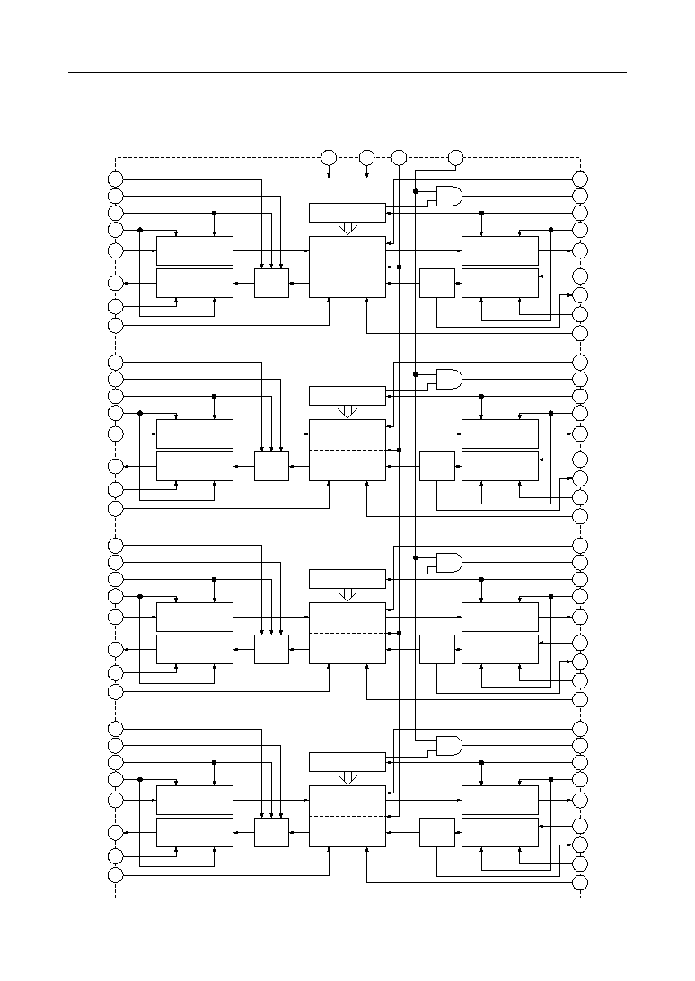
BLOCK DIAGRAM
PAD11
PAD10
SYXP1
BCKP1
SIP1
SOP1
SYRP1
RES1
PLL
CODER
DECODER
CODER
S
P
DECODER
S
P
PAD/
MUTE
MCK
CODER
P
S
DECODER
P
S
"0000"
DETECT
THR1
PLCK1
SYXA1
BCKA1
SOA1
SYRA1
PDN1
SIA1
DET1
PAD21
PAD20
SYXP2
BCKP2
SIP2
SOP2
SYRP2
RES2
PLL
CODER
DECODER
CODER
S
P
DECODER
S
P
PAD/
MUTE
MCK
CODER
P
S
DECODER
P
S
"0000"
DETECT
THR2
PLCK2
SYXA2
BCKA2
SOA2
SYRA2
PDN2
SIA2
DET2
PAD31
PAD30
SYXP3
BCKP3
SIP3
SOP3
SYRP3
RES3
PLL
CODER
DECODER
CODER
S
P
DECODER
S
P
PAD/
MUTE
MCK
CODER
P
S
DECODER
P
S
"0000"
DETECT
THR3
PLCK3
SYXA3
BCKA3
SOA3
SYRA3
PDN3
SIA3
DET3
PAD41
PAD40
SYXP4
BCKP4
SIP4
SOP4
SYRP4
RES4
PLL
CODER
DECODER
CODER
S
P
DECODER
S
P
PAD/
MUTE
MCK
CODER
P
S
DECODER
P
S
"0000"
DETECT
THR4
PLCK4
SYXA4
BCKA4
SOA4
SYRA4
PDN4
SIA4
DET4
0 V
LAW
+2.7 V to 5.5 V
V
DD
PLCKEN
GND
3/18
° Semiconductor
MSM7581
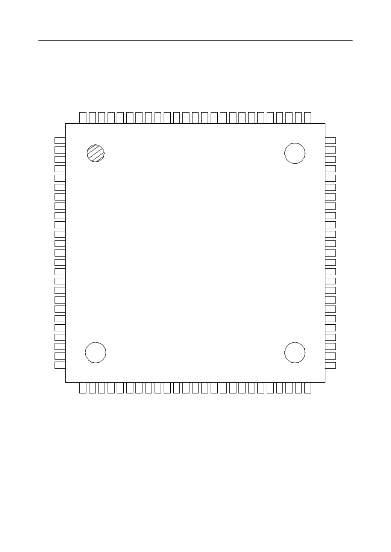
PIN CONFIGURATION (TOP VIEW)
100
NC
RES1
SYRP1
SIP1
SOP1
BCKP1
NC
SYXP1
PAD10
PAD11
NC
GND
V
DD
PLCKEN
NC
PAD41
PAD40
SYXP4
NC
BCKP4
SOP4
SIP4
SYRP4
RES4
NC
NC
RES2
SYRP2
SIP2
SOP2
BCKP2
NC
SYXP2
PAD20
PAD21
NC
V
DD
GND
LAW
NC
PAD31
PAD30
SYXP3
NC
BCKP3
SOP3
SIP3
SYRP3
RES3
NC
NC
THR1
PLCK1
SYXA1
SOA1
SIA1
NC
DET1
SYRA1
BCKA1
NC
PDN1
NC
PDN2
NC
BCKA2
SYRA2
DET2
NC
SIA2
1
2
3
4
5
6
7
8
9
10
11
12
13
14
15
16
17
18
19
20
SOA2
SYXA2
PLCK2
THR2
NC
21
22
23
24
25
NC
THR4
PLCK4
SYXA4
SOA4
SIA4
NC
DET4
SYRA4
BCKA4
NC
PDN4
NC
PDN3
NC
BCKA3
SYRA3
DET3
NC
SIA3
75
74
73
72
71
70
69
68
67
66
65
64
63
62
61
60
59
58
57
56
SOA3
SYXA3
PLCK3
THR3
NC
55
54
53
52
51
99
98
97
96
95
94
93
92
91
90
89
88
87
86
85
84
83
82
81
80
79
78
77
76
26
27
28
29
30
31
32
33
34
35
36
37
38
39
40
41
42
43
44
45
46
47
48
49
50
NC : No connect pin
100-Pin Plastic TQFP

4/18
° Semiconductor
MSM7581
PIN AND FUNCTIONAL DESCRIPTIONS
GND
Ground, 0 V.
SIP1, SOP1
PCM serial data input (SIP1) and output (SOP1) for Channel 1.
SOP1 is an open-drain output, which goes into a high impedance state after a continuous 8-bit
serial data output.
SIP2, SOP2
PCM serial data input (SIP2) and output (SOP2) for Channel 2.
SOP2 is an open-drain output, which goes into a high impedance state after a continuous 8-bit
serial data output.
SIP3, SOP3
PCM serial data input (SIP3) and output (SOP3) for Channel 3.
SOP3 is an open-drain output, which goes into a high impedance state after a continuous 8-bit
serial data output.
SIP4, SOP4
PCM serial data input (SIP4) and output (SOP4) Channel 4.
SOP4 is an open-drain output, which goes into a high impedance state after a continuous 8-bit
serial data output.
PAD10 - PAD40, PAD11 - PAD41
PAD mode control.
The PCM output can be attenuated by 12 dB or 6 dB and set to an out-of-service pattern (idle
pattern) by controlling these pins. Set these pins to digital "0" level during normal operation.The
control sequences are as follows:
PAD11 - PAD41
PAD10 - PAD40
0
0
0
1
1
0
1
1
Normal
6 dB Loss
12 dB Loss
Out-of-service Pattern

5/18
° Semiconductor
MSM7581
THR1, THR2, THR3, THR4
Control pins for the data-through modes.
THR (1 - 4) are for Channel (1 - 4), respectively. The data-through mode is selected when digital
"1" is applied to THR (1 - 4). In this mode, 8-bit serial input data applied to SIA (1 - 4) (ADPCM
data input) is passed to the PCM serial data output pins, SOP (1 - 4), without any data
modification. SOP (1 - 4) go to the high impedance state after the output of 8-bit data has been
applied to SIA (1 - 4).
Conversely 8-bit serial input data applied to SIP (1 - 4) (PCM data input) is passed to ADPCM
serial data output pins, SOA (1 - 4), without any data modification.
SOA (1 - 4) go to the high impedance state after the output of 8-bit serial data has been applied
to SIP (1 - 4).
ADPCM and PCM data interfaces have the mutually independent signal input pins for
synchronizing signals. The time slots for data input and output can be exchanged between them.
Some timing at which data may be deleted or duplicated as described in "Note on Usage" should
not be used.
SYXP1 - 4, SYRP1 - 4
Synchronous signal input pins to define PCM data input and output timing for Channel 1 (SIP1,
SOP1), Channel 2 (SIP2, SOP2), Channnel 3 (SIP3, SOP3), and Channel 4 (SIP4, SOP4).
The synchronous signals SYXA1 and SYRAI (Channel 1), SYXA2 and SYRA2 (Channel 2),
SYXA3 and SYRA3 (Channel 3), and SYXA4 and SYRA4 (Channel 4), which define ADPCM data
input and output timing are provided.
PCM and ADPCM data interfaces can be used at a mutually independent timing except some
timing.
Note: When PCM and ADPCM data interfaces are used at a mutually independent timing, the
timing described in "Note on Usage" should not be used.
SYXP signals must be input for PAD signal input processing.
BCKP1 - 4
Bit clock input.
These signals define the PCM data transmission speed at the PCM data input/output terminals.
BCKP (1 - 4) are used for Channel (1 - 4). Since BCKA (1 - 4) defines the data rate of the ADPCM
data interface, the PCM and ADPCM data can be input or output at different speeds.
LAW
PCM data companding law selection.
Digital "1" and "0" correspond to A-law and
µ
-law, respectively.
PDN1, PDN2, PDN3, PDN4
Power down mode selection.
PDN1 - 4 can be independently set to power down mode. When digital "0" is applied, these pins
are in the power-down mode.