 | –≠–ª–µ–∫—Ç—Ä–æ–Ω–Ω—ã–π –∫–æ–º–ø–æ–Ω–µ–Ω—Ç: MSM7603B | –°–∫–∞—á–∞—Ç—å:  PDF PDF  ZIP ZIP |

° Semiconductor
MSM7603/7603B
1/20
° Semiconductor
MSM7603/7603B
Echo Canceler
GENERAL DESCRIPTION
The MSM7603/7603B is an improved version of the MSM7602 with basically the same
configuration, and offers twice the cancelable echo delay time of the MSM7602.
The MSM7603B I/O interface allows switching between m-law PCM and A-law PCM.
The MSM7603/7603B is a low-power CMOS IC device for canceling echo (in an acoustic system
or telephone line) generated in a speech path.
Echo is canceled, in digital signal processing, by estimating the echo path and generating a
pseudo echo signal.
When used as an acoustic echo canceler, the device can cancel the acoustic echo, between the loud
speaker and the microphone, which occur during hands free communication such as on a cellular
phone or a conference system phone.
When used as a line echo canceler, the device can cancel the line echo which returns due to
impedance mismatching in a hybrid.
In addition, a quality conversation is made possible by controlling the level and by preventing
howling through a howling detector, double talk detector, attenuation function and a gain
control function, and by controlling the low level noise by means of a center clipping function.
The use of a single chip codec, such as the MSM7704 (3 V) and MSM7533 (5 V), allows an economic
and efficient echo canceler to be configured.
FEATURES
∑ Can handle both acoustic and telephone line echoes.
∑ Switchable between m-law PCM and A-law PCM interfaces. (MSM7603B)
∑ Cancelable echo delay time:
MSM7603B-003 .............. 55 ms (max.)
∑ Echo attenuation
: 30 dB (typ.)
∑ Clock frequency
: 19.2 MHz
17.5 MHz to 20 MHz (when internal sync signal not used)
∑ Power supply voltage : 2.7 V to 5.5 V
∑ Package:
28-pin plastic SSOP (SSOP28-P-485-0.65-K) (Product name : MSM7603-003GS-K)
(Product name : MSM7603B-003GS-K)
E2U0064-18-82
This version: Aug. 1998
° Semiconductor
MSM7603/7603B
2/20
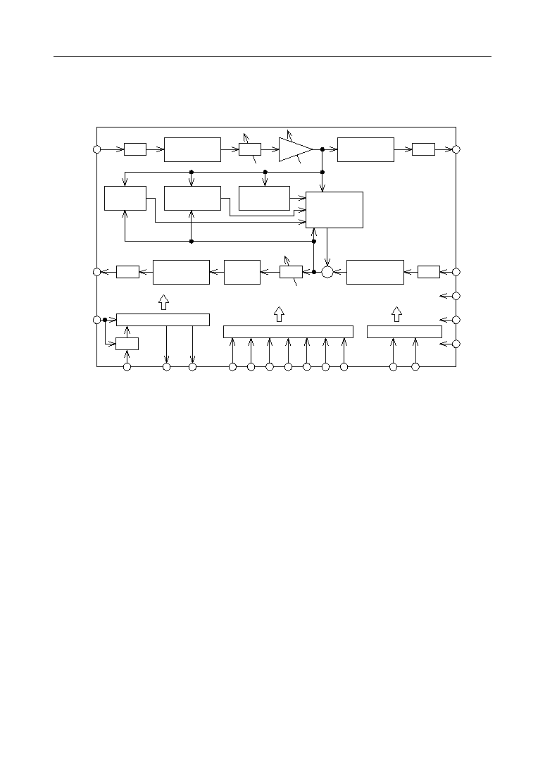
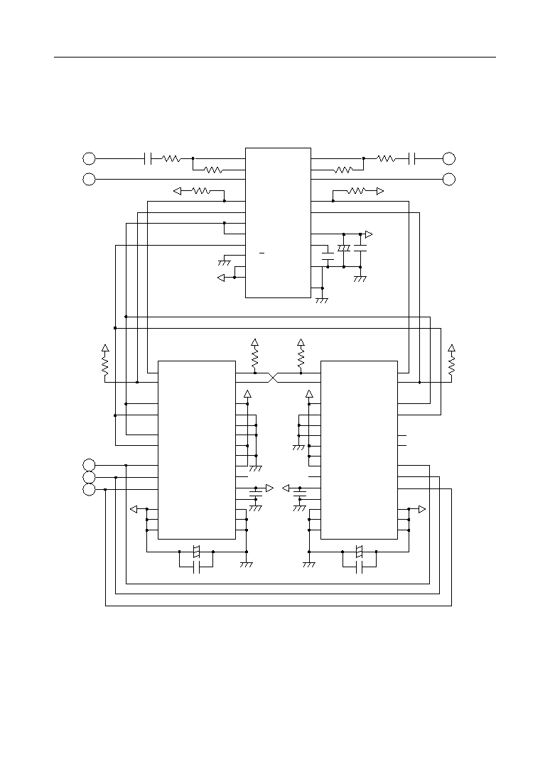
BLOCK DIAGRAM
MSM7603/7603B
Howling
Detector
Double Talk
Detector
Power
Calculator
Adaptive
FIR Filter
(AFF)
Non≠linear/
Linear
S/P
ATT
Gain
Linear/
Non≠linear
P/S
Non≠linear/
Linear
S/P
+
+
≠
ATT
Linear/
Non≠linear
P/S
Center
Clip
RIN
ROUT
SOUT
SIN
RST
V
DD
V
SS
PWDWN
Clock Generator
Mode Selector
I/O Controller
SCK
SYNC
NLP HCL ADP ATT GC
SYNCO
SCKO
CLKIN
PLL
HD m/A
*
For MSM7603B only
° Semiconductor
MSM7603/7603B
3/20
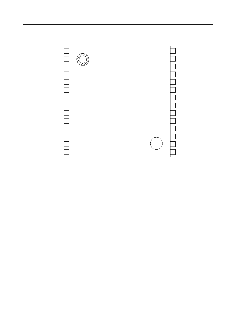
PIN CONFIGURATION (TOP VIEW)
1
2
3
4
5
6
7
8
9
10
11
12
13
14
28
27
26
25
24
23
22
21
20
19
18
17
16
15
NLP
HCL
ADP
SYNC
SCK
V
DD
V
SS
RST
PWDWN
HD
V
DD
[m/A]
*
CLKIN
V
DD
(PLL)
V
SS
(PLL)
V
DD
SOUT
ROUT
SIN
RIN
V
SS
NC
NC[TEST]
*
V
DD
ATT
SCKO
GC
SYNCO
V
SS
NC : No connect pin
28-Pin Plastic SSOP
*
Pins shown in brackets apply to MSM7603B.
° Semiconductor
MSM7603/7603B
4/20
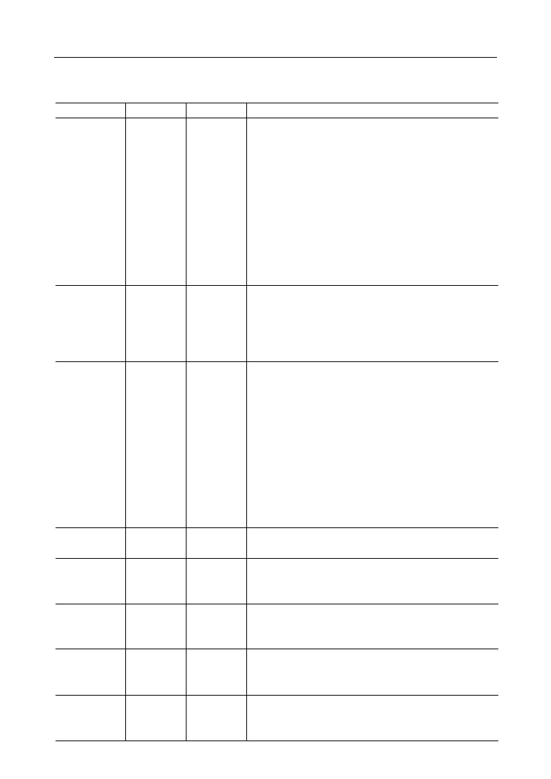
PIN DESCRIPTIONS
Pin
Symbol
Type
Description
1
NLP
I
2
HCL
I
3
ADP
I
4
SYNC
I
5
SCK
I
This is the control pin for the center clipping function to force
the SOUT output to a minimum value when the SOUT signal is
below ≠57 dBm0. Effective for reducing low-level noise.
"H": Center clip ON
"L": Center clip OFF
This is the through mode control pin.
When this pin is in the through mode the RIN and SIN data are
output to ROUT and SOUT. At the same time, the coefficient of
the adaptive FIR filter is cleared.
"H": Through mode
"L": Normal mode (echo canceler operates)
This is the AFF coefficient control pin which stops updating the
adaptive FIR filter (AFF) coefficient and sets it to a fixed value,
when the pin is configured to be the coefficient fix mode.
Used when holding the AFF coefficient which has been once
converged.
"H": Coefficient fix mode
"L": Normal mode (coefficient update)
This is the input pin for the sync signal for transmit/receive
serial data. This pin uses the external SYNC or SYNCO.
Inputs the PCM codec transmit/receive sync signal (8 kHz).
This is the clock input pin for transmit/receive serial data. It
uses the external SCK or the SCKO.
Input the PCM codec transmit/receive clock (64 to 2048 kHz).
° Semiconductor
MSM7603/7603B
5/20
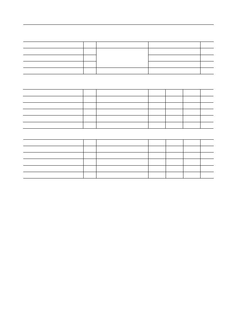
PIN DESCRIPTIONS (Continued)
Pin
Symbol
Type
Description
8
RST
I
9
PWDWN
I
10
HD
I
12
CLKIN
I
16
SYNCO
O
This is the input pin for the reset signal.
"L": Reset mode
"H": Normal operation mode
Due to initialization, input signals are disabled for 100 ms after reset
(after RST is returned from "L" to "H").
Input the basic clock during the reset.
Output pins during the reset are in the following sates :
High impedance: SOUT, ROUT
Not affected: SYNCO, SCKO
This is the power-down mode control pin for power down operation
"L": Power-down mode
"H": Normal operation mode
During power-down mode, all input pins are disabled and output
pins are in the following states :
High impedance : SOUT, ROUT
"L": SYNCO, SCKO
Reset after the power-down mode is released.
This pin controls the howling detect function that detects and
cancels a howling generated during hands-free talking for
acoustic system.
This function is used to cancel acoustic echoes.
"L": Howling detector ON
"H": Howling detector OFF
This is the input pin for external input for the basic clock.
Input the basic clock (17.5 to 20 MHz).
When the internal sync signal (SYNCO, SCKO) is used, input the
basic clock of 19.2 MHz.
This is the output pin for the 8 kHz sync signal for the PCM codec.
Connect to the SYNC pin and the PCM codec transmit/receive sync
pin.
Leave open if using an external SYNC.
11
(m/A)
I
Used for MSM7603B only.
This is the input pin for m-law PCM/A-law PCM interface select
signal.
"L": A-law PCM interface
"H": m-law PCM interface
For MSM7603, apply V
DD
.
13
V
DD
(PLL)
I
This is the power supply pin for the PLL circuit used for the basic
clock.
Insert a 0.1 mF capacitor with excellent high frequency
characteristics between V
DD
(PLL) and V
SS
(PLL).
14
V
SS
(PLL)
I
This is the ground pin for the PLL circuit used for the basic clock.
° Semiconductor
MSM7603/7603B
6/20
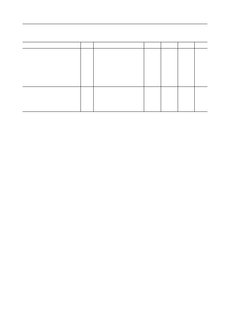
PIN DESCRIPTIONS (Continued)
Pin
Symbol
Type
Description
26
ROUT
O
27
SOUT
O
25
SIN
I
24
RIN
I
18
SCKO
O
17
GC
I
19
ATT
I
This is the pin for the input signal by which the gain controller
for the RIN input is controlled. The pin also controls RIN input
level and prevents howling.
The gain controller adjusts the RIN input level when it is ≠20
dBm0 or above. RIN input levels from ≠20 to ≠11.5 dBm0 will be
suppressed to ≠20 dBm0 in the attenuation range from 0 to 8.5 dB.
RIN input levels above ≠11.5 dBm0 will always be attenuated by
8.5 dB.
"H": Gain control ON
"L": Gain control OFF
"H" is recommended for performing echo cancellation.
This is the output pin for the transmit clock signal (256 kHz) for
the PCM codec.
Connect to the SCK pin and the PCM codec transmit/receive clock
pin.
Leave open when using an external SCK.
This is the control pin for the ATT function which prevents howling
by attenuators (ATT) for the RIN input and SOUT output.
If there is input only to RIN, then the ATT for the SOUT output is
activated.
If there is no input to SIN or there is input to both SIN and RIN,
then the ATT for the RIN input is activated.
Either the ATT for the RIN output or the ATT for the SOUT is
always activated in all cases, and the attenuation of ATT is 6 dB.
"H": ATT OFF
"L": ATT ON
"L" is recommended for performing echo cancellation.
This is the receive serial data input pin.
Input the PCM signal synchronized to SYNC and SCK.
Data is read at the falling edge of SCK.
This is the transmit serial data input pin.
Input the PCM signal synchronized to SYNC and SCK.
Data is read at the falling edge of SCK.
This is the output pin for receive serial data.
Outputs the PCM signal synchronized to SYNC and SCK.
This pin is in high impedance state during the absence of data output.
This is the output pin for transmit serial data.
Outputs the PCM signal synchronized to SYNC and SCK.
This pin is in high impedance state during the absence of data output.
21
(TEST)
O
This pin is for MSM7603B only and not used. Should be left open.
In MSM7603 it is an NC pin.
° Semiconductor
MSM7603/7603B
7/20
ABSOLUTE MAXIMUM RATINGS
Parameter
Power Supply Voltage
Input Voltage
Power Dissipation
Storage Temperature
Symbol
V
DD
V
IN
P
D
T
STG
Condition
Ta = 25∞C
--
Rating
≠0.3 to
+ 7
≠0.3 to V
DD
+ 0.3
1
≠55 to
+150
Unit
V
V
W
∞C
RECOMMENDED OPERATING CONDITIONS
Parameter
Power Supply Voltage
Power Supply Voltage
High Level Input Voltage
Low Level Input Voltage
Operating Temperature
Symbol
V
DD
V
SS
V
IH
V
IL
Ta
Condition
--
--
--
--
--
Min.
2.7
--
2.0
0
≠40
Unit
V
V
V
V
∞C
Typ.
3.3
0
--
--
+25
Max.
3.6
--
V
DD
0.5
+85
(V
DD
= 2.7 V to 3.6 V)
Parameter
Power Supply Voltage
Power Supply Voltage
High Level Input Voltage
Low Level Input Voltage
Operating Temperature
Symbol
V
DD
V
SS
V
IH
V
IL
Ta
Condition
--
--
--
--
--
Min.
4.5
--
2.4
0
≠40
Unit
V
V
V
V
∞C
Typ.
5
0
--
--
+25
Max.
5.5
--
V
DD
0.8
+85
(V
DD
= 4.5 V to 5.5 V)

° Semiconductor
MSM7603/7603B
8/20
ELECTRICAL CHARACTERISTICS
DC Characteristics
(V
DD
= 2.7 V to 3.6 V, Ta = ≠40∞C to +85∞C)
Parameter
High Level Output Voltage
Low Level Output Voltage
High Level Input Current
Low Level Input Current
High Level Output Leakage Current
Low Level Output Leakage Current
Power Supply Current
(Operating)
Power Supply Current
(Standby)
Input Capacitance
Output Load Capacitance
Symbol
V
OH
V
OL
I
IH
I
IL
I
OZH
I
OZL
I
DDO
I
DDS
C
I
C
LOAD
Condition
I
OH
= 40 mA
I
OL
= 1.6 mA
V
IH
= V
DD
V
IL
= V
SS
V
OH
= V
DD
V
OL
= V
SS
--
PWDWN = "L"
--
--
Min.
2.2
0
--
≠1
--
≠1
--
--
--
--
Typ.
--
--
0.1
≠0.1
0.1
≠0.1
30
0.5
--
--
Max.
V
DD
0.4
1
--
1
--
50
1
15
20
Unit
V
V
mA
mA
mA
mA
mA
mA
pF
pF
(V
DD
= 4.5 V to 5.5 V, Ta = ≠40∞C to +85∞C)
Parameter
High Level Output Voltage
Low Level Output Voltage
High Level Input Current
Low Level Input Current
High Level Output Leakage Current
Low Level Output Leakage Current
Power Supply Current
(Operating)
Input Capacitance
Output Load Capacitance
Power Supply Current
(Standby)
Symbol
V
OH
V
OL
I
IH
I
IL
I
OZH
I
OZL
I
DDO
I
DDS
C
I
C
LOAD
Condition
I
OH
= 40 mA
I
OL
= 1.6 mA
V
IH
= V
DD
V
IL
= V
SS
V
OH
= V
DD
V
OL
= V
SS
--
PWDWN = "L"
--
--
Min.
Typ.
4.2
--
0
--
--
0.1
≠10
≠0.1
--
0.1
≠10
≠0.1
--
40
--
0.5
--
--
--
--
Max.
V
DD
0.4
10
--
10
--
70
1
15
20
Unit
V
V
mA
mA
mA
mA
mA
mA
pF
pF
° Semiconductor
MSM7603/7603B
9/20
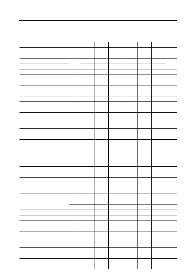
Echo Canceler Characteristics (Refer to Characteristics Diagram)
Parameter
Echo Attenuation
Cancelable Echo Delay Time
Symbol
L
RES
T
D
Condition
R
IN
= ≠10 dBm0
(5 kHz band white noise)
E. R. L. (echo return loss)
= 6 dB
T
D
= 50 ms
ATT, GC, NLP: OFF
R
IN
= ≠10 dBm0
(5 kHz band white noise)
E. R. L. = 6 dB
ATT, GC, NLP: OFF
Min.
Typ.
Max.
Unit
--
30
--
dB
--
--
55
ms
° Semiconductor
MSM7603/7603B
10/20
AC Characteristics
Parameter
Clock Frequency
When Internal Sync Signal is not used
Clock Cycle Time
When Internal Sync Signal is not used
Clock Duty Ratio
Clock "H" Level Pulse Width
fc = 19.2 MHz
Clock "L" Level Pulse Width
fc = 19.2 MHz
Clock Rise Time
Clock Fall Time
Sync Clock Output Time
Internal Sync Clock Frequency
Internal Sync Clock Output Cycle Time
Internal Sync Clock Duty Ratio
Internal Sync Signal Output Delay Time
Internal Sync Signal Period
Internal Sync Signal Output Width
Transmit/Receive Sync Clock Frequency
Transmit/Receive Sync Clock Cycle Time
Transmit/Receive Sync Clock Duty Ratio
Transmit/Receive Sync Signal Period
Sync Timing
Sync Signal Width
Receive Signal Setup Time
Receive Data Input Time
Serial Output Delay Time
Symbol
f
C
t
MCK
t
DMC
t
MCH
t
MCL
t
r
t
f
t
DCM
f
CO
t
CO
t
DCO
t
DCC
t
CYO
t
WSO
f
SCK
t
SCK
t
DSC
t
CYC
t
XS
t
SX
t
WSY
t
DS
t
ID
t
SD
t
XD
t
WR
Min.
--
17.5
--
50.0
40
20.8
20.8
--
--
--
--
--
64
0.488
40
123
45
t
SCK
--
1
Typ.
19.2
--
52.08
--
--
--
--
256
3.9
50
125
t
CO
--
--
50
125
--
--
7t
SCK
--
Max.
--
20.0
--
57.14
60
31.3
31.3
--
--
--
--
--
2048
15.6
60
--
t
CYC
-t
SCK
--
--
--
Min.
--
17.5
--
50.0
40
20.8
20.8
--
--
--
--
--
--
--
--
--
64
0.488
40
123
45
45
t
SCK
45
--
--
--
1
Typ.
19.2
--
52.08
--
--
--
--
--
--
--
256
3.9
50
--
125
t
CO
--
--
50
125
--
--
--
--
7t
SCK
--
--
--
Max.
--
20.0
--
57.14
60
31.3
31.3
5
5
40
--
--
--
5
--
--
2048
15.6
60
--
--
t
CYC
-t
SCK
--
--
--
90
90
--
Unit
MHz
ns
ns
ns
ns
ns
ns
ns
kHz
ms
%
ns
ms
ms
kHz
ms
%
ms
ns
ns
ms
ns
ms
ns
ns
ms
V
DD
= 2.7 V to 3.6 V
V
DD
= 4.5 V to 5.5 V
(Ta = ≠40∞C to +85∞C)
Reset Start Time
t
DRS
5
--
--
ns
Reset End Time
t
DRE
--
--
52
ns
Processing Operation Start Time
t
DIT
100
--
--
100
--
--
ms
Reset Signal Input Width
Power Down Start Time
Power Down End Time
t
DPS
--
--
--
--
111
15
ns
t
DPE
ns
Control Pin Hold Time (RST)
t
DHR
20
--
--
ns
Control Pin Setup Time (RST)
t
DSR
20
--
--
ns
--
--
--
--
--
--
5
5
40
--
--
5
45
--
--
45
--
--
--
--
--
--
90
90
5
--
--
--
--
52
--
--
20
20
--
--
--
--
111
15
--
--
Control Pin Setup Time
t
DTS
0
--
--
ns
0
--
--
Control Pin Hold Time
t
DTH
160
--
--
ns
160
--
--
Reset Pulse Width Immediately after Power Down t
WPR
10
--
--
ns
10
--
--
Receive Signal Hold Time
t
DH
45
--
--
ns
45
--
--
° Semiconductor
MSM7603/7603B
11/20
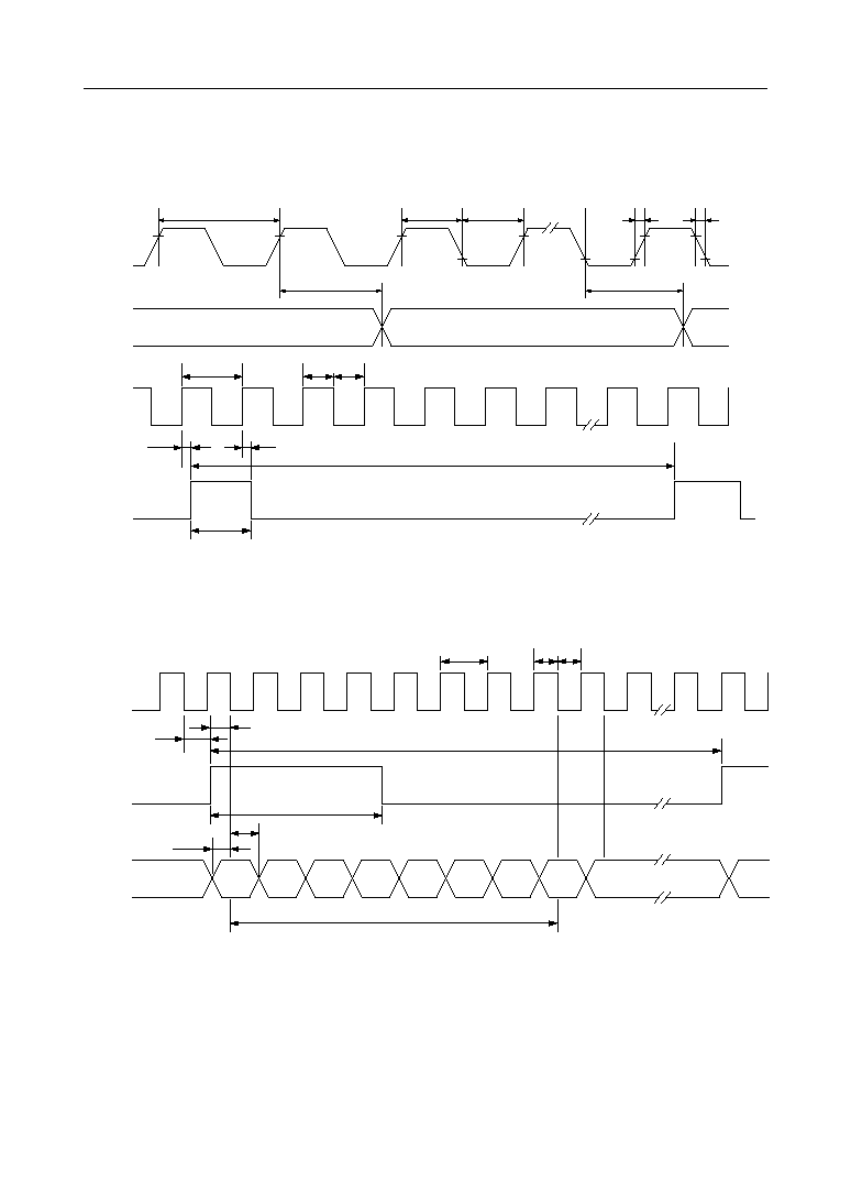
TIMING DIAGRAM
Clock Timing
CLKIN
t
r
t
f
t
MCH
t
MCL
f
C
, t
MCK
, t
DMC
SCKO
t
DCM
SCKO
SYNCO
t
CYO
t
DCO
t
DCC
t
DCC
t
WSO
f
CO
, t
CO
t
DCM
Serial Input Timing
SCK
SYNC
SIN
RIN
MSB
7
t
CYC
f
SCK
, t
SCK
t
SX
t
XS
t
WSY
t
DS
6
5
4
3
2
1
LSB
0
MSB
7
t
DSC
t
ID
t
DH
° Semiconductor
MSM7603/7603B
12/20
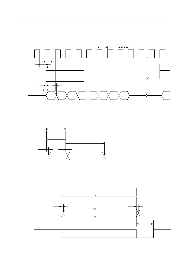
Serial Output Timing
Operation Timing After Reset
Power Down Timing
t
DPS
t
DPE
Internal Operation
Processing Start
Power Down
PWDWN
t
WPR
Invalid
RST
SCK
SYNC
SOUT
ROUT
MSB
7
t
CYC
f
SCK
, t
SCK
t
SX
t
XS
t
WSY
t
SD
6
5
4
3
2
1
LSB
0
MSB
7
t
DSC
High-Z
t
XD
t
XD
High-Z
t
DRS
RST
t
WR
t
DRE
Internal operaion
,
Processing Start
t
DIT
Reset
Initialization
*Reset timing can be asynchronous.
* INT is invalid during the shaded interval.
° Semiconductor
MSM7603/7603B
13/20
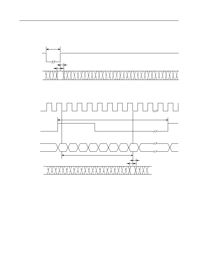
Control Pin Load-in Timing
NLP, HCL, HD,
ATT, ADP, GC
t
DHR
RST
t
WR
t
DSR
SCK
SYNC
SIN
MSB
7
t
CYC
t
ID
6
5
4
3
2
1
LSB
0
MSB
7
RIN
NLP, HCL, HD,
ATT, ADP, GC
t
DTH
t
DTS
° Semiconductor
MSM7603/7603B
14/20
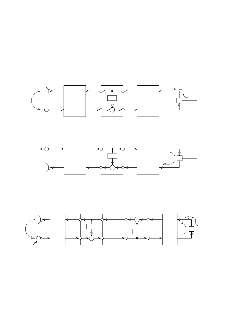
HOW TO USE THE MSM7603/7603B
The MSM7603/7603B cancels, based on the RIN signal, the echo which returns to SIN.
Connect the base signal to the R side and the echo-generated signal to the S side.
Connection Methods According to Echoes
Example 1:
Canceling acoustic echo (to handle acoustic echo from line input)
+
+
≠
AFF
ROUT
SIN
RIN
SOUT
MSM7603
MSM7603B
CODEC
CODEC
H
Line input
Acoustic echo
Example 2:
Canceling line echo (to handle line echo from microphone input)
+
+
≠
AFF
RIN
SOUT
ROUT
SIN
MSM7603
MSM7603B
CODEC
CODEC
H
Lin echo
Microphone input
Example 3: Canceling of both acoustic and line echo
(to handle both acoustic echo from line input and line echo from microphone input)
SIN
ROUT
CODEC
H
Line input
Acoustic echo
+
+
≠
AFF
ROUT
SIN
MSM7603
MSM7603B
+
+
≠
AFF
SOUT
RIN
MSM7603
MSM7603B
RIN
SOUT
Microphone input
For acoustic echo
Line echo
CODEC
For line echo
° Semiconductor
MSM7603/7603B
15/20
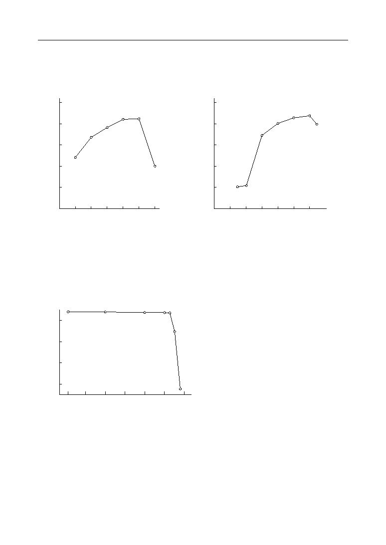
ECHO CANCELER CHARACTERISTICS DIAGRAM
(for
m
m
m
m
m-law and A-law, and for reference only)
0
10
20
30
40
40
30
20
10
0
E. R. L. vs. echo attenuation
Echo attenuation [dB]
E. R. L. [dB]
Measurement Conditions :
RIN input = ≠10 dBm0 5 kHz band white noise
Echo delay time T
D
= 50 ms
ATT, GC, NLP = OFF
Power supply voltage 5 V
0
10
20
30
40
≠50 ≠40 ≠30 ≠20 ≠10
0
RIN input level vs. echo attenuation
Echo attenuation [dB]
RIN input level [dBm0]
Measurement Conditions :
RIN input: 5 kHz band white noise
Echo delay time T
D
= 50 ms
E.R.L. = 6 dB
ATT, GC, NLP = OFF
Power supply voltage 5 V
0
10
20
30
0
Echo delay time vs. echo attenuation
Echo attenuation [dB]
Echo delay time [ms]
50
Measurement Conditions :
RIN input = ≠10 dBm
5 kHz band white noise
E.R.L. = 6 dB
ATT, GC, NLP = OFF
Power supply voltage 5 V
10
20
30
40
≠10
Note:
Above characteristics are for the MSM7533 (V
DD
5 V, m-law CODEC interface). For the
MSM7704 (V
DD
3 V, m-law interface) the characteristics are basically the same except
for input and output levels. Refer to the PCM CODEC data sheet.
MSM7533
(for both transmit and receive)
0 dBm0 = 0.85 Vrms = 0.8 dBm (600 W)
MSM7704
(for transmit side)
0 dBm0 = 0.35 Vrms = ≠6.9 dBm (600 W)
(for receive side)
0 dBm0 = 0.5 Vrms = ≠3.8 dBm (600 W)
° Semiconductor
MSM7603/7603B
16/20
Measurement System Block Diagram
RIN
SOUT
ROUT
SIN
MSM7603B
Delay
T
D
Echo delay time
ATT
E. R. L.
(Echo Return Loss)
Power supply voltage 5 V
RIN
SOUT
L. P. F.
5 kHz
Level meter
White noise generator
2ch CODEC
MSM7533
MSM7603
° Semiconductor
MSM7603/7603B
17/20
APPLICATION CIRCUIT
Bidirectional Connection Example
Microphone input
C1
R1
Speaker output
DV
R3
21
22
4
13
12
14
10
16
19
5
6
DV
AIN1
GSX1
AOUT1
DOUT1
DIN1
XSYNC
RSYNC
BCLK
A / m
PDN
CHP
AIN2
GSX2
AOUT2
DOUT2
DIN2
V
DD
SGC
AG
DG
24
23
2
14
11
8
1
18
9
R2
R5
DV
R7
R6
AV
+
C9
C10 C11
C5
Line input
Line output
(AG)
MSM7603/7603B
For cancelation of
acoustic echo
MSM7603/7603B
For cancelation of line echo
DV
R8
DV
R4
25
26
4
5
16
18
9
8
12
6
20
28
DV
PWDWN
RST
CLK
27
24
1
2
19
17
11
13
7
15
23
3
10
14
SIN
ROUT
SYNC
SCK
SYNCO
SCKO
RST
PWDWN
CLKIN
V
DD
V
DD
V
DD
SOUT
RIN
NLP
HCL
ATT
GC
V
DD
(P)
V
SS
V
SS
V
SS
ADP
HD
(m / A)
V
SS
(P)
SOUT
RIN
NLP
HCL
ATT
GC
(m / A)
V
DD
(P)
V
SS
V
SS
V
SS
ADP
HD
V
SS
(P)
SIN
ROUT
SYNC
SCK
SYNCO
SCKO
RST
CLKIN
V
DD
V
DD
V
DD
PWDWN
27
24
1
2
19
17
11
13
7
15
23
3
10
14
C4
C8
DV
DV
DV
25
26
4
5
16
18
9
8
12
6
20
28
DV
+
C6
C7
C2
C3
+
R1=20 kW
R2=20 kW
R3=2.2 kW
R4=10 kW
R9=10 kW
C1=1 mF
C2=10 mF
C3=0.1 mF
C4=0.1 mF
R5=20 kW
R6=20 kW
R7=2.2 kW
R8=10 kW
R10=10 kW
C5=1 mF
C6=10 mF
C7=0.1 mF
C8=0.1 mF
C9=0.1 mF
C10=10 mF
C11=0.1 mF
Use the MSM7704-01GS-VK as a PCM CODEC when V
DD
3 V is used.
The MSM7533 is pin compatible with the MSM7704.
2ch CODEC
MSM7533VGS-K
DV
DV
R9
R10
21
(TEST)
21
(TEST)

° Semiconductor
MSM7603/7603B
18/20
NOTES ON USE
1. Set echo return loss (ERL) to be attenuated. If the echo return loss is set to be
amplified, the echo cannot be eliminated.
Refer to the characteristics diagram for E. R. L. vs. echo attenuation quantity.
2. Set the level of the analog input so that the PCM codec does not overflow.
3. The recommended input level is ≠10 to ≠20 dBm0. Refer to the characteristics
diagram for the RIN input level vs. echo attenuation quantity.
4. Applying the tone signal to this echo canceler for long duration may decrease echo
attenuation.
When used with the HD pin "L" (howling detector ON), this echo canceler may
operate faultily if, while a signal is input to the RIN pin, a tone signal with a higher
level than the signal being input to RIN is input to the SIN pin.
A signal should therefore be input either to the RIN pin or to the SIN pin. If,
however, the tone signal is input to the SIN pin while a signal is input to the RIN pin,
the ADP, HD, or HCL pin must be set to "H".
5. For changes in the echo path (retransmit, circuit switching during transmission,
and so on), convergence may be difficult.
Perform a reset to make it converge.
If the state of the echo path changes after a reset, convergence may again be difficult.
In cases such as a change in the echo path, perform a reset each time.
6. When turning the power ON, set the PWDWN pin to "1" and input the basic clock
simultaneously with power ON.
If the device is put into power down mode immediately after power ON, be sure
to input 10 or more clocks of the basic clock before setting to the power down mode.
7. After power ON, be sure to reset the device.
8. After the power down mode is released (when PWDWN pin is changed to a "1" from
a "0"), be sure to reset the device.
9. If this canceler is used to cancel acoustic echoes, an echo attenuation may be less
than 30 dB.

° Semiconductor
MSM7603/7603B
19/20
EXPLANATION OF TERMS
Attenuating Function :
This function prevents howling and controls the noise level with
the attenuator for the RIN input and SOUT output. Refer to the
explanation of pins (ATT pin).
Echo Attenuation :
If there is talking (input only to RIN) in the path of a rising echo
arises, the echo attenuation refers to the difference in the echo
return loss (canceled amount) when the echo canceler is not used
and when it is used.
Echo attenuation = (SOUT level during through mode operation)
≠ (SOUT level during echo canceler operation) [dB]
Echo Delay Time :
This is the time from when the signal is output from ROUT until it
returns to SIN as an echo.
Acoustic Echo :
When using a hands-free phone, for example, the signal output
from the speaker echoes and is input again to the microphone. The
return signal is referred to as acoustic echo.
Telephone Line Echo :
This is a signal which is delayed midway in a telephone line and
returns as an echo, due to reasons such as a hybrid impedance
mismatch.
Gain Control Function :
This function prevents howling and controls the sound level by
with a gain controller for the RIN input. Refer to the explanation
of pins (GC pin).
Center Clipping Function : This function forces the SOUT output to a minimum value when
the signal is below ≠57 dBm0. Refer to the explanation of pins (NLP
pin).
Double Talk Detection :
Double talk refers to a state in which the SIN and RIN signals are
input simultaneously. In a double talk state, a signal other than the
echo signal which is to be canceled can be input to the SIN input,
resulting in malfunction.
The double talk detector prevents such malfunction of the canceler.
Howling Detection :
This is the oscillating state caused by the acoustic coupling between
the loud speaker and the microphone during hands-free talking.
Howling not only interferes with talking, but can also cause
malfunction of the echo canceler.
The howling detector prevents such malfunction and howling.
Echo Return Loss (ERL) :
When the signal output from ROUT returns to SIN as an echo, ERL
refers to how much loss there is in the signal level during ROUT.
ERL = (ROUT level) ≠ (SIN level of the ROUT signal which returns
as an echo) [dB]
If ERL is positive (ROUT > SIN), acts as an attenuator.
If ERL is negative (ROUT < SIN), acts as an amplifier.
PHS :
Personal Handyphone System

° Semiconductor
MSM7603/7603B
20/20
(Unit : mm)
PACKAGE DIMENSIONS
Notes for Mounting the Surface Mount Type Package
The SOP, QFP, TSOP, SOJ, QFJ (PLCC), SHP and BGA are surface mount type packages, which
are very susceptible to heat in reflow mounting and humidity absorbed in storage.
Therefore, before you perform reflow mounting, contact Oki's responsible sales person for the
product name, package name, pin number, package code and desired mounting conditions
(reflow method, temperature and times).
SSOP28-P-485-0.65-K
Package material
Lead frame material
Pin treatment
Solder plate thickness
Package weight (g)
Epoxy resin
42 alloy
Solder plating
5 mm or more
0.39 TYP.
Mirror finish