 | –≠–ª–µ–∫—Ç—Ä–æ–Ω–Ω—ã–π –∫–æ–º–ø–æ–Ω–µ–Ω—Ç: MSM7617 | –°–∫–∞—á–∞—Ç—å:  PDF PDF  ZIP ZIP |

1/28
° Semiconductor
MSM7617
GENERAL DESCRIPTION
The MSM7617 cancels echoes (acoustic or line echoes) generated in voice channels. It is a low-
power CMOS LSI device with two channels.
MSM7617 echo canceling is performed by digital signal processing. It negates echoes by
estimating the echo channel and then generating a pseudo-echo signal.
When used as an acoustic echo canceler, the MSM7617 can cancel acoustic echoes between
speaker and microphone that occur during hands-free speaking with car phones, conferencing
system phones, etc. When used as a line echo canceler, the MSM7617 can cancel line echoes
returned by hybrid impedance mismatches.
By setting its mode for use as a single cross-connected channel, the MSM7617 can cancel both
acoustic and line echoes.
Also, the MSM7617 can improve voice communication by using its howling detection, double-
talk detection, attenuation, and gain control functions to prevent and suppress howling levels,
and by using its center clipping function to suppress low level noise.
Furthermore, the MSM7617 can disable echo canceling during data communication with its 2100
Hz tone detector and 2100 Hz phase reversal detector. It also provides the ability to attenuate SIN
levels, to amplify SOUT levels, and to adjust input/output levels.
An economical and highly efficient echo canceler unit can be constructed by using a 2-channel
single-chip CODEC like the MSM7533 together with the MSM7617.
° Semiconductor
MSM7617
2-Channel Echo Canceler
E2U0057-38-21
This version: Feb. 1999
Previous version: Aug. 1998

2/28
° Semiconductor
MSM7617
FEATURES
∑Echo canceler has two channels, which can be used for acoustic and line echoes. Set as a single
cross-connected channel, it can be used for both acoustic and line echoes.
∑ITU-T G164/G165 standard tone disabler.
∑PCM line level adjustment possible with SIN level attenuator (SA pin) and SOUT level
amplifier (SG pin). Can also be used for ERL amplification with the SIN level attenuator (SA
pin).
∑RGC pin provides input/output adjustment mode (
±
6LR mode) that can prevent malfunction
due to excessive inputs without changing the RIN-ROUT input/output levels.
∑Cancelable echo delay time:
55 ms (max.)
∑Echo attenuation:
30 dB (typ.)
∑Clock frequency:
18 to 20 MHz
19.2 MHz if using internal clock signal
∑Power supply voltage:
4.5 to 5.5 V
∑Package:
64-pin plastic QFP (QFP64-P-1414-0.80-BK)
∑Product name:
MSM7617-001GS-BK (m-law)
3/28
° Semiconductor
MSM7617
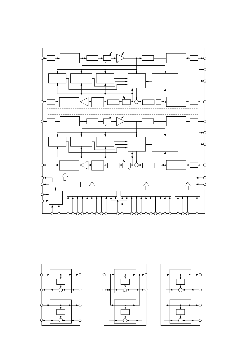
BLOCK DIAGRAM
S/P
≠6LR
+6LR
P/S
Non-linear/
Linear
Linear/
Non-linear
Adaptive
FIR Filter
(AFF)
P/S
S/P
Linear/
Non-linear
Non-linear/
Linear
SG
Center
Clip
+6LR
ATT
Howling
Detector
Double Talk
Detector
Power
Calculator
+
≠6LR
ROUT1
SA
2100 Hz Tone,
Phase Reverse
Detector
RIN1
DF1
WDT1
SIN1
SOUT1
ATT
GC
S/P
≠6LR
+6LR
P/S
Non-linear/
Linear
Linear/
Non-linear
Adaptive
FIR Filter
(AFF)
P/S
S/P
Linear/
Non-linear
Non-linear/
Linear
SG
Center
Clip
+6LR
ATT
Howling
Detector
Double Talk
Detector
Power
Calculator
+
≠6LR
ROUT2
SA
2100 Hz Tone,
Phase Reverse
Detector
RIN2
DF2
WDT2
SIN2
SOUT2
ATT
GC
CH1
CH2
≠
≠
+
+
V
DD
SYNCO
V
SS
SCKO
Clock Generator
V
DD
(PLL)
V
SS
(PLL)
PLL
EC-A Controller
EC-B Controller
I/O Controller
IOM0,1
SYNC2
SYNC1
SCK
GC20,21
SA20,21
SG20,21
ATT2
HD2
RST2
ADP2
HCL2
NLP2
ECM
SA10,11
SG10,11
ATT1
HD1
RST1
ADP1
HCL1
NLP1
PWDWN
CLKIN
ECDM0,1
RGC1011
The above diagram shows internal connections for 2-channel parallel mode. The internal
connections for 2-channel serial I/O mode and 1-channel cross-connected mode are shown
below.
CH1
ROUT1
RIN1
SIN1
SOUT1
RIN
ROUT
SOUT
SIN
+
AFF
CH2
ROUT2
RIN2
SIN2
SOUT2
RIN
ROUT
SOUT
SIN
+
AFF
2-channel parallel I/O mode
CH1
RIN1
SIN1
SOUT1
RIN
ROUT
SOUT
SIN
+
AFF
CH2
RIN
ROUT
SOUT
SIN
+
AFF
2-channel serial I/O mode
CH1
ROUT1
SIN1
RIN
ROUT
SOUT
SIN
+
AFF
CH2
ROUT2
SIN2
RIN
ROUT
SOUT
SIN
+
AFF
1-channel cross-connected mode
ROUT1
4/28
° Semiconductor
MSM7617
PIN CONFIGURATION (TOP VIEW)
48
47
46
45
44
43
42
41
40
39
38
1
2
3
4
5
6
7
8
9
10
11
RST2
ADP2
HCL2
SYNC2
V
DD
NLP2
IOM0
IOM1
SCK
ECM
NLP1
V
SS
(PLL)
V
DD
(PLL)
CLKIN
V
SS
V
SS
TST
PWDWN
ECDM1
ECDM0
SCKO
SYNCO
64
63
62
61
60
59
58
57
56
55
54
HD2
ATT2
SOUT2
SIN2
V
SS
ROUT2
RIN2
SG21
SG20
SA21
SA20
17
18
19
20
21
22
23
24
25
26
27
HD1
ATT1
SOUT1
SIN1
V
DD
ROUT1
RIN1
SG11
SG10
SA11
SA10
12
V
SS
13
SYNC1
14
HCL1
15
ADP1
16
RST1
28
V
SS
29
RGC11
30
RGC10
31
DF1
32
WDT1
37 V
DD
36 V
DD
35 V
DD
34 V
DD
33 V
DD
53
V
DD
52
RGC21
51
RGC20
50
DF2
49
WDT2
64-Pin Plastic QFP
5/28
° Semiconductor
MSM7617
PIN DESCRIPTIONS
Pin
Symbol
Type
Description
1
RST2
I
Reset signal input pin for channel 2.
"L": Reset
"H": Normal operation
Input signals are invalid for 100 ms after reset (after RST returns to "H"
from "L") for setting initial values.
Input the basic clock during reset. Output pins will be placed in the
following states during reset.
Hi-Z: ROUT2, SOUT2
No effect: SYNCO, SCKO, ROUT1, SOUT1, DF1, WDT1
Previous state: DF2, WDT2
2
ADP2
I
AFF coefficient control pin for channel 2.
This pin stops coefficient variation of the adaptive FIR filter (AFF), fixing the
coefficients. It allows once acquired AFF coefficients to be saved.
"H": Fixed coefficient mode
"L": Normal mode (variable coefficients)
3
HCL2
I
Echo canceler disable pin for channel 2.
This pin disables the echo canceler and enables data from SIN to SOUT to be output
in "through mode". The input and output levels of SIN and SOUT are changed by the
setting of the SG and SA pins; therefore, to output data from SIN to SOUT in
"through mode", set the SA and SG pins to "0 dB".
It simultaneously clears the adaptive FIR filter coefficients.
"H": Disable mode
"L": Normal mode (echo canceller enabled)
4
SYNC2
I
Sync signal input pin for channel 2 transmit/receive PCM data while in
parallel I/O mode.
Input the transmit/receive sync signal (8 kHz) of the PCM CODEC connected
to channel 2. Input "L" if not in parallel I/O mode.
6
NLP2
I
NLP control pin for channel 2.
This pin controls center clipping, forcing SOUT2 output to the minimum
positive value when it is below ≠54 dBm0. It is effective for reducing
uncanceled echoes and low-level noise.
"H": Center clipping on
"L": Center clipping off
7
8
IOM0
IOM1
I
Sets I/O mode of PCM data.
IOM0
0
1
0
1
Mode Setting
2-channel parallel I/O mode
2-channel serial I/O mode
1-channel cross-connected mode
Inhibited
IOM1
0
0
1
1
6/28
° Semiconductor
MSM7617
PIN DESCRIPTIONS (Continued)
Pin
Symbol
Type
Description
10
ECM
I
Not used. Fix input to "H".
13
SYNC1
I
Sync signal input pin for channel 1 transmit/receive PCM data while in 2-
channel parallel I/O mode, 2-channel serial I/O mode, or 1-channel cross-
connected mode.
Input the transmit/receive sync signal (8 kHz) of the PCM CODEC.
14
HCL1
I
Echo canceler disable control pin for channel 1.
This pin disables the echo canceler and enables data from SIN to SOUT to be output
in "through mode". The input and output levels of SIN and SOUT are changed by the
setting of the SG and SA pins; therefore, to output data from SIN to SOUT in "through
mode", set the SA and SG pins to "0 dB".
It simultaneously clears the adaptive FIR filter coefficients.
"H": Disable mode
"L": Normal mode (echo canceler enabled)
15
ADP1
I
AFF coefficient control pin for channel 1.
This pin stops coefficient variation of the adaptive FIR filter (AFF), fixing the
coefficients. It allows once acquired AFF coefficients to be saved.
"H": Fixed coefficient mode
"L": Normal mode (variable coefficients)
16
RST1
I
Reset signal input pin for channel 1.
"L": Reset
"H": Normal operation
Input signals are invalid for 100 ms after reset (after RST returns to "H" from
"L") for setting initial values.
Input the base clock during reset. Output pins will be placed in the following
states during reset.
Hi-Z: ROUT1, SOUT1
No effect: SYNCO, SCKO, ROUT2, SOUT2, DF2, WDT2
Previous state: DF1, WDT1
11
NLP1
I
NLP control pin for channel 1.
This pin controls center clipping, forcing SOUT1 output to the minimum
positive value when it is below ≠54 dBm0. It is effective for reducing
uncancelled echoes and low-level noise.
"H": Center clipping on
"L": Center clipping off
9
SCK
I
Common pin for channel 1 and channel 2. Clock input pin for PCM data
transmission.
Input the same clock as the transmit/receive clock of the PCM CODEC.
Frequencies below 128 kHz cannot be used in serial mode.
7/28
° Semiconductor
MSM7617
Pin
Symbol
Type
Description
18
ATT1
I
ATT control pin for channel 1.
This pin controls the ATT function for preventing howling with the
attenuators (ATT) provided on RIN and SOUT. When input is only on RIN,
the SOUT attenuator is activated. When there is no input on RIN or there is
input on both SIN and RIN, the RIN input attenuator is activated. Either the
ATT for the RIN output or the ATT for the SOUT is always activated in all
cases, and the attenuation of ATT is 6 dB.
"H": Attenuator off
"L": Attenuator on
Because the attenuator is inserted opposite the speaker, it is effective for
further reducing echo.
19
SOUT1
O
PCM data output pin. Output signal changes depending on the setting of
the IOM pins (refer to the block diagram).
Data is always output on the rising edge of SCK. This pin is put in high
impedance state while there is no data or during reset.
In 2-channel parallel I/O mode, this pin becomes SOUT for channel 1 and
outputs the PCM signal synchronous with SYNC1. In 2-channel serial I/O
mode, this pin outputs the SOUT signal as a multiplexed PCM signal of
SOUT signal for channel 1 and channel 2 synchronous with SYNC1.
In 1-channel cross-connected mode, this pin becomes high impedance.
17
HD1
I
Howling detection control pin for channel 1.
This pin controls detection and canceling of howling generated by the
acoustics of handsfree telephones.
"L": Howling detector on
"H": Howling detector off
PIN DESCRIPTIONS (Continued)

8/28
° Semiconductor
MSM7617
Pin
Symbol
Type
Description
22
ROUT1
O
PCM data output pin. Output signal changes depending on the setting of
the IOM pins (refer to the block diagram).
Data is always output on the rising edge of SCK. This pin becomes high
impedance while there is no data or during reset.
In 2-channel parallel I/O mode, this pin becomes ROUT for channel 1 and
outputs the PCM signal synchronous with SYNC1. In 2-channel serial I/O
mode, this pin outputs the ROUT signal as a multiplexed PCM signal of ROUT
signals for channel 1 and channel 2 synchronous with SYNC1.
In 1-channel cross-connected mode, this pin becomes the cross-connected
ROUT pin for channel 1, and outputs the PCM signal synchronous with SYNC1.
23
RIN1
I
PCM data input pin. Pin use changes depending on the setting of the IOM
pins (refer to the block diagram).
In 2-channel parallel I/O mode, this pin becomes RIN for channel 1 and
inputs the PCM signal synchronous with SYNC1. In 2-channel serial I/O
mode, this pin sequentially inputs RIN as a multiplexed PCM signal from
channel 1 and channel 2 synchronous with SYNC1. In 1-channel cross-
connected mode, this pin is not used, and should be fixed at "L".
Data is captured on the falling edge of SCK.
20
SIN1
I
PCM data input pin. Pin use changes depending on the setting of the IOM
pins (refer to the block diagram).
In 2-channel parallel I/O mode, this pin becomes SIN for channel 1 and
inputs the PCM signal synchronous with SYNC1. In 2-channel serial I/O
mode, this pin sequentially inputs SIN as a multiplexed PCM signal from
channel 1 and channel 2 synchronous with SYNC1. In 1-channel cross-
connected mode, this pin becomes the cross-connected SIN pin for channel
1, and inputs the PCM signal synchronous with SYNC1.
Data is captured on the falling edge of SCK.
PIN DESCRIPTIONS (Continued)
9/28
° Semiconductor
MSM7617
Pin
Symbol
Type
Description
29
30
RGC11
RGC10
I
R input level control pins for channel 1 (refer to the block diagram).
Excessive input (PCM level is at maximum value) causes a malfanction.
Use these pins when there is a possibility of excessive input.
RGC10
0
1
0
1
Level Control Mode
Off
GC: On (control level = ≠20 dBm0)
By the R gain controller, levels from ≠20 to ≠11.5 dBm0 will
be suppressed to ≠20 dBm0 and those above ≠11.5 dBm0 will
always be attenuated by 8.5 dB. This is effective to prevent
excessive input and howling for hands-free applications.
Inhibited
±6LR: On
Applies ≠6 dB to excessive inputs using the level adjuster
provided on R and S I/O. Since +6 dB also is applied at the
output, the total level will not change, making this effective
against line echo.
24
25
SG11
SG10
I
S output gain control pins for channel 1 (refer to the block diagram).
These pins amplify the output level of SOUT. The gain level can be set even
during the echo canceler disable mode.
26
27
SA11
SA10
I
S input attenuator control pins for channel 1 (refer to the block diagram).
These pins attenuate the input level of SIN. Use them if ERL is large.
The attenuation level can be set even during the echo canceler disable mode.
SG10
0
1
0
1
Gain Level
0 dB
+6 dB
+12 dB
Not used
SA10
0
1
0
1
Attenuation Level
0 dB
≠6 dB
≠12 dB
Not used
SG11
0
0
1
1
SA11
0
0
1
1
RGC11
0
0
1
1
PIN DESCRIPTIONS (Continued)
10/28
° Semiconductor
MSM7617
Pin
Symbol
Type
Description
40
41
ECDM0
ECDM1
I
Tone disabler control pin common to channel 1 and channel 2.
These pins detect answer tones generated by modems (2100 Hz), and then
disable the echo canceler.
42
PWDWN
I
Common pin for channel 1 and channel 2.
This pin controls the power-down mode to reduce current consumption
when the device is not being used.
"L": Power down
"H": Normal operation
During power-down mode all input pins are invalid, and output pins will enter
the following states.
Hi-Z: SOUT1, SOUT2, ROUT1, ROUT2
"L": SYNCO, SCKO
Previous state: DF1, WDT1, DF2, WDT2
Reset the device after power-down mode is released.
Tone Disabler Mode
Off
2100 Hz tone detection: On
2100 Hz and phase reversal detection: On
Inhibited
ECDM0
0
1
0
1
31
DF1
O
Tone disabler flag output pin for channel 1.
This pin outputs a disable flag when the ECDM pins are used for tone disabler
mode.
"H": Echo canceler disabled
"L": Echo canceler enabled
39
SCKO
O
Output pin for internal SCK signal (256 kHz).
This pin is used for the transfer clock of PCM signals. Connect it to the PCM
CODEC's synchronization signal pin. Leave open if using an external SYNC.
32
WDT1
O
Not used. Leave this pin open.
38
SYNCO
O
Output pin for internal SYNC signal (8 kHz).
This pin is used as the transmit/receive synchronization signal for PCM signals.
Connect it to the SYNC pin and PCM CODEC's synchronization signal pin. Leave
this pin open if using an external SYNC.
ECDM1
0
0
1
1
PIN DESCRIPTIONS (Continued)
11/28
° Semiconductor
MSM7617
Pin
Symbol
Type
Description
51
52
RGC20
RGC21
I
R input level control pins for channel 2 (refer to the block diagram).
Excessive input (PCM level is at maximum value) causes a malfunction.
Use these pins when there is a possibility of excessive input.
Level Control Mode
Off
GC: On (control level = ≠20 dBm0)
By the R gain controller, levels from ≠20 to ≠11.5 dBm0
will be suppressed to ≠20 dBm0 and those above ≠11.5
dBm0 will always be attenuated by 8.5 dB. This is
effective to prevent excessive input and howling for
hands-free applications.
Inhibited
±6LR: On
Apply ≠6 dB to excessive inputs using the level
adjuster provided on R and S I/O. Since +6 dB also
is applied at the output, the total level will not
change, making this effective against line echo.
RGC20
0
1
0
1
RGC21
0
0
1
1
47
V
DD
(PLL)
I
Power supply for PLL circuit that uses the basic clock.
Insert a 0.1mF capacitor with excellent high frequency characteristics
between V
DD
(PLL) and V
SS
(PLL).
43
TST
O
Not used. Leave this pin open.
46
CLKIN
I
Basic clock input pin.
Input a clock 18 to 20 MHz. Use 19.2 MHz if using internal synchronization
signals (SYNCO, SCKO).
48
V
SS
(PLL)
I
Ground for PLL circuit that uses the basic clock.
Insert a 0.1mF capacitor with excellent high frequency characteristics
between V
DD
(PLL) and V
SS
(PLL).
49
WDT2
O
Not used. Leave this pin open.
50
DF2
O
Tone disabler flag output pin for channel 2.
This pin outputs a disable flag when the ECDM pins are used for tone
disabler.
"H": Echo canceler disabled
"L": Echo canceler enabled
PIN DESCRIPTIONS (Continued)
12/28
° Semiconductor
MSM7617
Pin
Symbol
Type
Description
58
RIN2
I
PCM data input pin. Pin use changes depending on the setting of the IOM
pins (refer to the block diagram).
In 2-channel parallel I/O mode, this pin becomes RIN for channel 2 and
inputs the PCM signal synchronous with SYNC2. Data is captured on the
falling edge of SCK. In other modes, this pin is not used, and should be
fixed at "L".
59
ROUT2
O
PCM data output pin. Output signal changes depending on the setting of
the IOM pins (refer to the block diagram).
Data is always output on the rising edge of SCK. This pin becomes high
impedance while there is no data.
In 2-channel parallel I/O mode, this pin becomes ROUT for channel 2 and
outputs the PCM signal synchronous with SYNC2. In 2-channel serial I/O
mode, this pin is not used and should be left open. In 1-channel cross-
connected mode, this pin becomes the cross-connected ROUT pin for
channel 2, and outputs the PCM signal synchronous with SYNC1.
54
55
SA20
SA21
I
S input attenuator control pins for channel 2 (refer to the block diagram).
These pins attenuate the input level of SIN. Use them if ERL is large.
The attenuation level can be set even during the echo canceler disable mode.
56
57
SG20
SG21
I
S output gain control pins for channel 2 (refer to the block diagram).
These pins amplify the output level of SOUT. The gain level can be set even
during the echo canceler disable mode.
SG20
0
1
0
1
Attenuation Level
0 dB
≠6 dB
≠12 dB
Not used
SG20
0
1
0
1
Gain Level
0 dB
+6 dB
+12 dB
Not used
SA21
0
0
1
1
SG21
0
0
1
1
PIN DESCRIPTIONS (Continued)
13/28
° Semiconductor
MSM7617
Pin
Symbol
Type
Description
63
ATT2
I
ATT control pin for channel 2.
This pin controls the ATT function for preventing howling with the
attenuators (ATT) provided on RIN and SOUT. When input is only on RIN,
the SOUT attenuator is activated. When there is no input on SIN or there is
input on both SIN and RIN, the RIN input attenuator is activated. Either the
ATT for the RIN output or the ATT for the SOUT is always activated in all
cases, and the attenuation of ATT is 6 dB.
"H": Attenuator off
"L": Attenuator on
Because the attenuator is activated opposite the speaker, it is effective for
further reducing echo.
64
HD2
I
Howling detection control pin for channel 2.
This pin controls detection and canceling of howling generated by the
acoustics of handsfree telephones.
"L": Howling detector on
"H": Howling detector off
61
SIN2
I
PCM data input pin. Pin use changes depending on the setting of the IOM
pins (refer to the block diagram). Data is captured on the falling edge of SCK.
In 2-channel parallel I/O mode, this pin becomes SIN for channel 2 and
inputs the PCM signal synchronous with SYNC2. In 2-channel serial I/O
mode, this pin is not used and should be fixed at "L". In 1-channel cross-
connected mode, this pin becomes the cross-connected SIN pin for channel
2, and inputs the PCM signal synchronous with SYNC1.
62
SOUT2
O
PCM data output pin. Output signal changes depending on the setting of
the IOM pins (refer to the block diagram).
Data is always output on the rising edge of SCK. This pin becomes high
impedance while there is no data.
In 2-channel parallel I/O mode, this pin becomes SOUT for channel 2 and
outputs the PCM signal synchronous with SYNC2. In other modes, this pin
is not used and should be left open.
PIN DESCRIPTIONS (Continued)
14/28
° Semiconductor
MSM7617
ABSOLUTE MAXIMUM RATINGS
Parameter
Power Supply Voltage
Power Supply Voltage
High Level Input Voltage
Operating Temperature
Symbol
V
DD
V
SS
V
IH
Ta
Condition
--
Unit
V
V
V
∞C
Low Level Input Voltage
V
IL
V
--
--
--
--
Min.
≠40
0
2.4
--
4.5
Typ.
+25
--
--
0
5
Max.
+85
0.8
V
DD
--
5.5
(V
DD
= 4.5 V to 5.5 V)
RECOMMENDED OPERATING CONDITIONS
ELECTRICAL CHARACTERISTICS
DC Characteristics
Parameter
High Level Output Voltage
Low Level Output Voltage
High Level Input Current
High Level Output Leakage Current
Symbol
V
OH
V
OL
I
IH
I
OZH
Condition
V
OH
= V
DD
Unit
V
V
µA
µA
Low Level Input Current
I
IL
µA
V
IL
= V
SS
V
IH
= V
DD
I
OL
= 1.6 mA
I
OH
= 40 µA
Min.
--
≠10
--
0
4.2
Typ.
0.1
≠0.1
0.1
--
--
Max.
10
--
10
0.4
V
DD
(V
DD
= 4.5 V to 5.5 V, Ta = ≠40∞C to +85∞C)
Low Level Output Leakage Current
Power Supply Current (operation mode)
Power Supply Current (power-down mode)
Output Load Capacitance
I
OZL
I
DDO
I
DDS
C
LOAD
--
µA
mA
mA
pF
Input Capacitance
C
I
pF
--
PWDWN = "L"
--
V
OL
= V
SS
--
--
≠10
--
--
≠0.1
20
15
--
--
80
130
--
0.5
2
Parameter
Power Supply Voltage
Input Voltage
Power Dissipation
Storage Temperature
Symbol
V
DD
V
IN
P
D
T
STG
Condition
Ta = 25∞C
--
Rating
≠0.3 to + 7
≠0.3 to V
DD
+ 0.3
1
≠55 to +150
Unit
V
V
W
∞C
15/28
° Semiconductor
MSM7617
Echo Canceler Characteristics (refer to characteristics diagram)
Parameter
Echo Reduction
(Common to Channel 1 and
Channel 2)
Symbol
L
RES
Condition
Unit
dB
R
IN
= ≠10 dBm0
(5 kHz white noise band)
E. R. L. = 6 dB
T
D
= 50 ms
ATT, GC, NLP: OFF
Min.
--
Typ.
30
Max.
--
Cancelable Echo Delay Time
(Common to Channel 1 and
Channel 2)
T
D
ms
R
IN
= ≠10 dBm0
(5 kHz white noise band)
E. R. L. = 6 dB
ATT, GC, NLP: OFF
--
--
55
Tone Disabler Characteristics
Parameter
Tone Detection
Phase Reversal Detection
Detection frequency
Detection level
Detection time
Detection frequency
Unit
Hz
dBm0
ms
Hz
Detection condition
Min.
2075
380
≠32
2075
Typ.
2100
--
--
2100
Max.
2125
2100Hz. 180∞ out-of-phase detected before and after 450±25ms.
--
--
2125
Release
Detection level
Phase reversal
Detection level
dBm0
∞
dBm0
≠32
--
--
135
180
225
--
--
≠32
Release time
ms
--
250
--
16/28
° Semiconductor
MSM7617
AC Characteristics
Parameter
Clock Frequency
If Used Without Internal Sync Signal
Clock Cycle Time
Clock Duty Cycle
Symbol
f
C
t
MCK
t
DMC
Unit
MHz
ns
%
If Used Without Internal Sync Signal
Min.
40
50
--
18
--
Typ.
--
--
52.08
--
19.2
Max.
60
55.56
--
20
--
(V
DD
= 4.5 V to 5.5 V, Ta = ≠40∞C to +85∞C)
Clock High Level Pulse Width
Clock Low Level Pulse Width
Clock Rise Time
Internal Sync Clock Output Time
t
MCH
t
MCL
t
r
t
DCM
ns
ns
ns
ns
Clock Fall Time
t
f
ns
--
--
t
MCK
• 0.4
--
--
--
40
5
t
MCK
• 0.6
Internal Sync Clock Frequency
f
CO
kHz
--
256
--
Internal Sync Clock Cycle Time
t
CO
µs
--
3.9
--
Internal Sync Clock Duty Cycle
t
DCO
%
--
50
--
Internal Sync Signal Output Time
t
DCC
ns
--
--
5
Internal Sync Signal Period
t
CYO
µs
--
125
--
Internal Sync Signal Pulse Width
t
WSO
µs
--
t
CO
--
Transmit/Receive Sync Clock Frequency
f
SCK
kHz
64
--
2048
In Serial I/O Mode
128
--
2048
Transmit/Receive Sync Clock Cycle Time
In Serial I/O Mode
Transmit/Receive Sync Clock Duty Cycle
t
DSC
%
40
50
60
Transmit/Receive Sync Signal Period
t
CYC
µs
--
125
--
Sync Timing
t
XS
ns
45
--
--
Receive Signal Setup Time
t
SX
ns
45
--
--
Receive Signal Hold Time
t
WSY
µs
t
SCK
--
t
CYC
≠t
SCK
Receive Signal Input Time
t
DS
ns
45
--
--
In 2-Channel Serial Mode
t
DH
ns
45
--
--
t
MCK
• 0.4
--
t
MCK
• 0.6
--
--
5
t
SCK
µs
0.488
--
15.62
0.488
--
7.81
t
ID
µs
--
7t
SCK
--
Sync Signal Width
t
ID2
µs
--
15t
SCK
--
17/28
° Semiconductor
MSM7617
Parameter
Serial Output Delay Time
Reset Signal Input Width
Symbol
t
SD
t
WR
Unit
ns
µs
Min.
1
--
--
Typ.
--
--
--
Max.
--
90
90
(V
DD
= 4.5 V to 5.5 V, Ta = ≠40∞C to +85∞C)
Reset Start Time
Reset End Time
Power-Down Start Time
t
DRS
t
DRE
t
DIT
t
DPE
ns
ns
µs
ns
Process Operation Start Time
t
DPS
ns
--
--
5
--
--
--
15
111
--
Power-Down End Time
t
WPR
ms
10
--
--
RST Width After Power-Down
t
DSR
ns
20
--
--
RST Control Pin Setup Time
t
DHR
ns
20
--
--
RST Control Pin Hold Time
t
DCS
ns
120
--
--
SCK Control Pin Setup Time
t
DCH
ns
120
--
--
SCK Control Pin Hold Time
--
--
52
100
--
--
ns
t
XD
AC Characteristics (Continued)
18/28
° Semiconductor
MSM7617
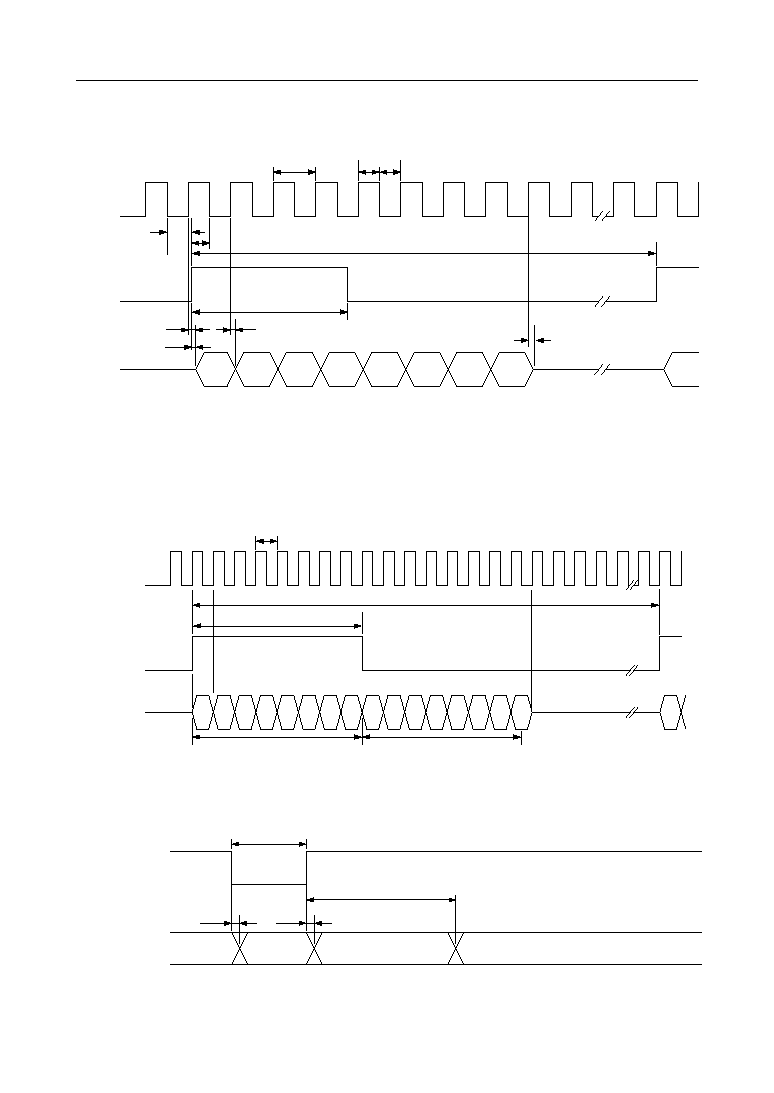
TIMING DIAGRAMS
Clock Timing
CLKIN
t
r
t
f
t
MCH
t
MCL
f
C
, t
MCK
, t
DMC
SCKO
t
DCM
SCKO
SYNCO
t
CYO
t
DCO
t
DCC
t
DCC
t
WSO
f
CO
, t
CO
t
DCM
19/28
° Semiconductor
MSM7617
Serial Data Input Timing (Parallel Mode, FTF Mode)
SCK
SYNC
SIN
RIN
MSB
7
t
CYC
f
SCK
, t
SCK
t
SX
t
XS
t
WSY
t
DS
6
5
4
3
2
1
LSB
0
MSB
7
t
DSC
t
ID
t
DH
Serial Data Input Timing (Serial Mode)
Note: Refer to parallel mode for detailed timing
SCK
SYNC1
RIN1
SIN1
t
CYC
f
SCK
, t
SCK
t
DS
t
DH
7
6
5
4
3
2
1
0
7
6
5
4
3
2
1
0
7
t
WSY
t
ID2
CH1 data
CH2 data
20/28
° Semiconductor
MSM7617
Serial Data Output Timing (Parallel Mode, FTF Mode)
SCK
SYNC
SOUT
ROUT
MSB
7
t
CYC
f
SCK
, t
SCK
t
SX
t
XS
t
WSY
t
XD
6
5
4
3
2
1
LSB
0
MSB
7
t
DSC
High-Z
t
XD
t
SD
High-Z
t
XD
Serial Data Output Timing (Serial Mode)
Note: Refer to parallel mode for detailed timing
SCK
SYNC1
ROUT1
SOUT1
t
CYC
f
SCK
, t
SCK
7
t
WSY
CH1 data
CH2 data
7
6
5
4
3
2
1
0
7
6
5
4
3
2
1
0
High-Z
High-Z
Operation Timing After Reset
t
DRS
RST
t
WR
t
DRE
Internal operation
Proccessing starts
t
DIT
Reset
Initial setting
Note: Reset timing can be asynchronous.

21/28
° Semiconductor
MSM7617
Power-Down Timing
Note: All inputs are invalid during power-down. Always reset the device after power-down.
t
DPS
t
DPE
t
WPR
Internal operation
,,
Power-down
PWDWN
RST
Capture Timing of Control Pins
Control pin states are captured during reset and during each period's serial data capture.
RST
t
WR
Control Pin
t
DSR
t
DHR
Channel 1 Control Pin
Channel 2 Control Pin
(when not in serial mode)
Channel 2 Control Pin (when in serial mode)
t
ID2
t
ID
t
DCS
t
DCH
t
DCS
t
DCH
SCK
SYNC
22/28
° Semiconductor
MSM7617
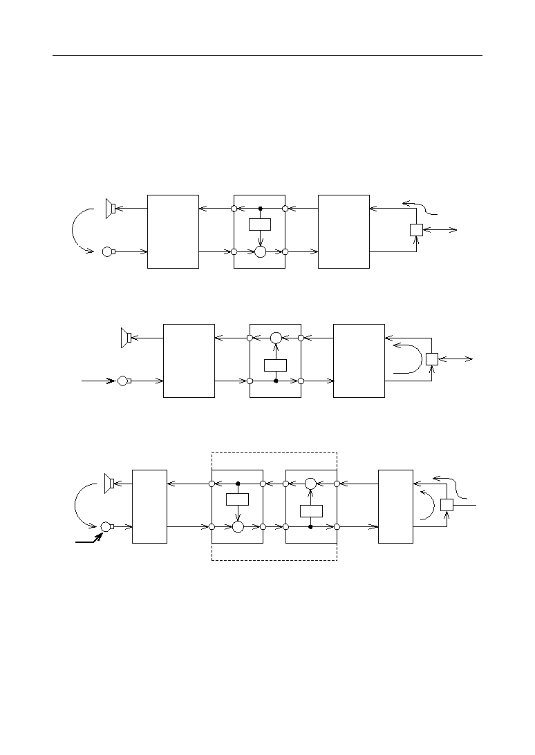
HOW TO USE THE MSM7617
The echo canceler cancels the echo on the RIN signal as returned by SIN. Connect the original
signal to the R side, and the signal generating the echo to the S side.
Connection Methods According to Echoes
Example 1. Cancel Acoustic Echo (applies to acoustic echo from line input)
+
+
≠
AFF
ROUT
SIN
RIN
SOUT
CODEC
CODEC
H
Input
Acoustic echo
Example 2. Cancel Line Echo (applies to line echo from microphone input)
AFF
SOUT
RIN
SIN
ROUT
CODEC
CODEC
H
Line echo
Input
+
Example 3. Cancel Both Acoustic Echo And Line Echo
SIN2
ROUT2
CODEC
H
Input
Acoustic echo
+
AFF
ROUT1
SIN1
MSM7617
+
AFF
Input
CH1
Line echo
CODEC
CH2
23/28
° Semiconductor
MSM7617
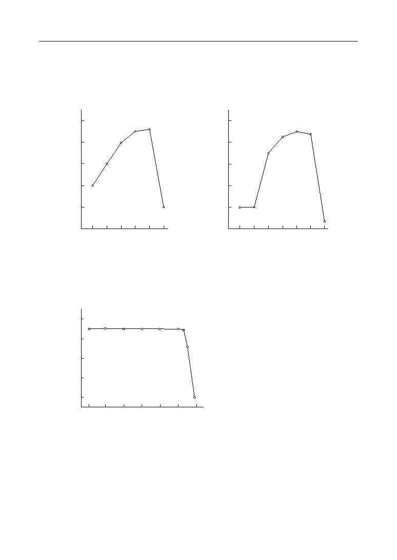
ECHO CANCELER CHARACTERISTICS DIAGRAM
Characteristics of m-law and A-law are identical. (Characteristic graphs below are reference
data.)
0
10
20
30
40
40
30
20
10
0
≠10
ERL vs. Echo Attenuation
Echo Attenuation [dB]
E. R. L. [dB]
Measuring Conditions:
RIN input level = ≠10 dBm0 white noise
Echo delay time = 50 ms
ATT, GC, NLP, LR all off
RIN Input Level vs. Echo Attenuation
Echo Attenuation [dB]
RIN Input level [dBm0]
Measuring Conditions:
RIN input = white noise
Echo delay time = 50 ms
E.R.L. = 6 [dB]
ATT, GC, NLP, LR all off
Echo Delay Time vs. Echo Attenuation
Echo Attenuation [dB]
Measuring Conditions:
RIN input level = ≠10 dBm0 white noise
Echo delay time = 50 ms
E.R.L = 6 dB
ATT, GC, NLP, LR all off
0
10
20
30
40
≠50 ≠40 ≠30 ≠20 ≠10
0
10
0
10
20
30
0
50
40
10
20
30
40
60
Echo Delay Time [ms]
Note: regarding dBm0:
The "dBm0" unit used in the characteristic graphs is a unit that expresses PCM CODEC digital
values. Therefore, be aware that the same value 0 [dBm0] might correspond to different analog
input levels depending on the PCM CODEC being used. Please check the data sheet of the PCM
CODEC being used.
Example
MSM7533
0 [dBm0] = 0.85 [Vrms] = 2.4 [Vp-p] = 0.8 [dBm] 600 W
≠10 [dBm0] = 0.27 [Vrms] = 0.76 [Vp-p] = ≠9.2 [dBm] 600 W
MSM7543
0 [dBm0] = 0.6007 [Vrms] = 1.7 [Vp-p] = ≠2.2 [dBm] 600 W
≠10 [dBm0] = 0.19 [Vrms] = 0.54 [Vp-p] = ≠12.2 [dBm] 600 W
24/28
° Semiconductor
MSM7617
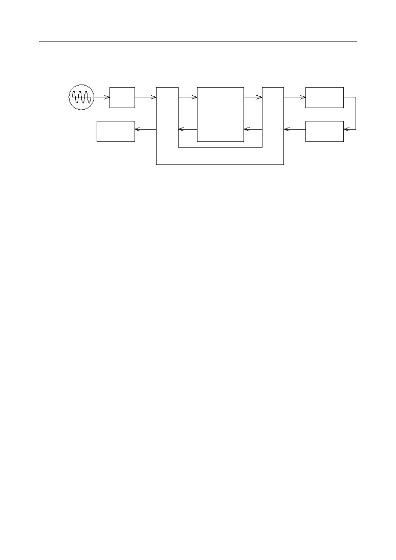
Measurement System Block Diagram
RIN
SOUT
ROUT
SIN
CH1 or CH2
Delay
Echo Delay Time
ATT
E. R. L.
2ch CODEC
L. P. F.
5 kHz
Level Meter
White noise generator
MSM7533
MSM7617

25/28
° Semiconductor
MSM7617
NOTES ON USE
1. Set echo return loss (E. R. L) to be attenuated. If the echo return loss is set to be amplified, the
echo cannot be canceled. (Refer to the "E. R. L vs Echo Attenuation" characteristic graph.)
When the echo return loss is amplified, adjust the input level to be attenuated by setting the
mode with the SA pin. If the level from the SA pin is too low by setting the mode with the SA
pin, then amplify the output level by setting the mode with the SG pin.
2. Set RIN input so that there is not excessive input (above 0 dBm0) from the PCM CODEC. Echo
cancellation is not possible with excessive input. (Refer to the "RIN vs Echo Attenuation"
characteristic graph.)
Recommended input levels are ≠10 to ≠20 dBm0. If there is a possibility of excessive input,
then set GC mode or 6LR mode with the RGC pins.
3. Applying the tone signals to this echo canceler will decrease echo attenuation.
4. For changes in the echo path (retransmit, circuit switching during transmission, and so on),
convergence may be difficult.
Perform a reset to make it converge.
If the state of the echo path changes after a reset, convergence may again be difficult.
In cases such as a change in the echo path, perform a reset each time.
5. If a clock is not input after power is applied, then the internal circuits will not stabilize,
possibly damaging the device.
When power is applied, set the PWDWN pin to "H" and input the basic clock.
If the device is put into PWDWN immediately after power has been applied, be sure to input
10 or more clocks of the basic clock before setting to the power down mode.
6. Always reset after power is applied or power-down is released.
For power-on reset operation, an external oscillator may require a certain setting time after
powered on. Allow 10 ms for a reset time after the oscillator has settled.
7. When the device is used as an acoustic echo canceler, equipment noise and environment noise
from the microphone amp may be amplified, and echo attenuation may be below 30 dB.
26/28
° Semiconductor
MSM7617
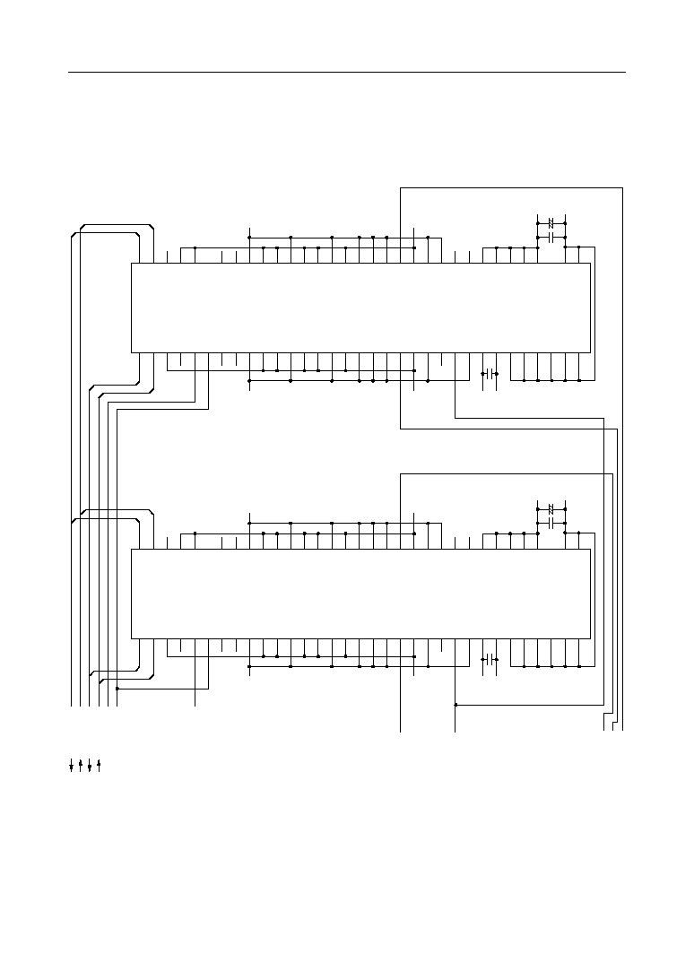
APPLICATION CIRCUITS
4-Channel Serial Interface
Line Echo Canceler Example
MSM7617
RIN1
ROUT1
23
22
SOUT1
SIN1
19
20
RIN2
ROUT2
58
59
SOUT2
SIN2
62
61
SYNC1
SYNC2
13
4
SCK
9
WDT1
WDT2
32
49
DF1
DF2
31
50
NLP1
NLP2
11
6
HCL1
HCL2
14
3
ADP1
ADP2
15
2
HD1
HD2
17
64
ATT1
ATT2
18
63
SG11
SG21
24
57
SG10
SG20
25
56
SA11
SA21
26
55
SA10
SA20
27
54
RGC11
RGC21
29
52
RGC10
RGC20
30
51
RST1
RST2
16
1
ECDM1
IOM1
41
8
ECDM0
IOM0
40
7
TST
ECM
43
10
CLKIN
SYNCO
46
38
PWDWN
SCKO
42
39
V
DD
(PLL)
V
SS
47
12
V
SS
(PLL)
V
SS
48
28
V
DD
V
SS
5
44
V
DD
V
SS
21
45
V
DD
V
SS
33
60
V
DD
34
V
DD
V
DD
35
37
V
DD
V
DD
36
53
ch1 SYNC
+5 V
GND
GND
CLOCK
GND
+5 V
+
+5 V
+5 V
GND
CH1
CH2
ch1 RST
MSM7617
RIN1
ROUT1
23
22
SOUT1
SIN1
19
20
RIN2
ROUT2
58
59
SOUT2
SIN2
62
61
SYNC1
SYNC2
13
4
SCK
9
WDT1
WDT2
32
49
DF1
DF2
31
50
NLP1
NLP2
11
6
HCL1
HCL2
14
3
ADP1
ADP2
15
2
HD1
HD2
17
64
ATT1
ATT2
18
63
SG11
SG21
24
57
SG10
SG20
25
56
SA11
SA21
26
55
SA10
SA20
27
54
RGC11
RGC21
29
52
RGC10
RGC20
30
51
RST1
RST2
16
1
ECDM1
IOM1
41
8
ECDM0
IOM0
40
7
TST
ECM
43
10
CLKIN
SYNCO
46
38
PWDWN
SCKO
42
39
V
DD
(PLL)
V
SS
47
12
V
SS
(PLL)
V
SS
48
28
V
DD
V
SS
5
44
V
DD
V
SS
21
45
V
DD
V
SS
33
60
V
DD
34
V
DD
V
DD
35
37
V
DD
V
DD
36
53
+5 V
GND
GND
GND
+5 V
+
+5 V
+5 V
GND
CH3
CH4
ch2 RST
ch3 RST
ch4 RST
SCK
ch3 SYNC
SOUT Bus
RIN Bus
SIN Bus
ROUT Bus
Terminal side
Line side
27/28
° Semiconductor
MSM7617
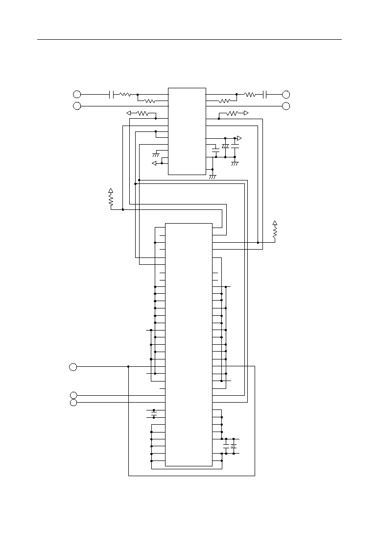
Cross-Connection Example
Microphone Input
Speaker Output
Line Input
Line Output
C2
R5
R6
24
23
2
14
11
8
1
18
9
C3
C4
C5
AV
+
(AG)
DV
R7
21
22
4
R2
R3
DV
R1
C1
13
12
15
10
16
19
5
6
DV
DV
R4
AIN1
GSX1
AOUT1
DOUT1
DIN1
XSYNC
RSYNC
BCLK
A/m
PDN
CHP
AIN2
GSX2
AOUT2
DOUT2
DIN2
V
DD
SGC
AG
DG
2ch CODEC
MSM7533VGS-K
DV
R8
MSM7617
22
20
59
61
4
DV
6
3
2
64
63
57
56
55
54
52
51
1
8
7
10
38
39
12
28
44
45
60
C7
C8
DG
+
DV
37
53
DG
DV
DG
DV
DG
23
19
58
62
13
9
49
50
32
31
11
14
15
17
18
24
25
26
27
29
30
16
41
40
43
46
42
47
48
5
21
33
35
36
34
C6
RST
PWDWN
CLK
RIN1
SOUT1
RIN2
SOUT2
SYNC1
SCK
WDT1
DF1
NLP1
HCL1
ADP1
HD1
ATT1
SG11
SG10
SA11
SA10
RGC11
RGC10
RST1
ECDM1
ECDM0
TST
CLKIN
PWDWN
V
DD
(PLL)
V
SS
(PLL)
V
DD
V
DD
V
DD
V
DD
V
DD
V
DD
ROUT1
SIN1
ROUT2
SIN2
SYNC2
WDT2
DF2
NLP2
HCL2
ADP2
HD2
ATT2
SG21
SG20
SA20
RGC21
RGC20
RST2
IOM1
IOM0
ECM
SYNC0
SCK0
V
SS
V
SS
V
SS
V
SS
V
DD
V
DD
R1 = 20 kW
R2 = 20 kW
R3 = 2.2 kW
R4 = 10 kW
R5 = 20 kW
R6 = 20 kW
R7 = 2.2 kW
R8 = 10 kW
C1 = 1 mF
C2 = 1 mF
C3 = 0.1 mF
C4 = 10 mF
C5 = 0.1 mF
C6 = 0.1 mF
C7 = 0.1 mF
C8 = 10 mF
SA21
28/28
° Semiconductor
MSM7617
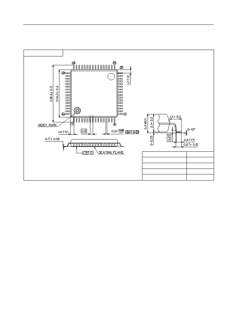
(Unit : mm)
PACKAGE DIMENSIONS
Notes for Mounting the Surface Mount Type Package
The SOP, QFP, TSOP, SOJ, QFJ (PLCC), SHP and BGA are surface mount type packages, which
are very susceptible to heat in reflow mounting and humidity absorbed in storage.
Therefore, before you perform reflow mounting, contact Oki's responsible sales person for the
product name, package name, pin number, package code and desired mounting conditions
(reflow method, temperature and times).
QFP64-P-1414-0.80-BK
Package material
Lead frame material
Pin treatment
Solder plate thickness
Package weight (g)
Epoxy resin
42 alloy
Solder plating
5 mm or more
0.87 TYP.
Mirror finish

NOTICE
1.
The information contained herein can change without notice owing to product and/or
technical improvements. Before using the product, please make sure that the information
being referred to is up-to-date.
2.
The outline of action and examples for application circuits described herein have been
chosen as an explanation for the standard action and performance of the product. When
planning to use the product, please ensure that the external conditions are reflected in the
actual circuit, assembly, and program designs.
3.
When designing your product, please use our product below the specified maximum
ratings and within the specified operating ranges including, but not limited to, operating
voltage, power dissipation, and operating temperature.
4.
Oki assumes no responsibility or liability whatsoever for any failure or unusual or
unexpected operation resulting from misuse, neglect, improper installation, repair, alteration
or accident, improper handling, or unusual physical or electrical stress including, but not
limited to, exposure to parameters beyond the specified maximum ratings or operation
outside the specified operating range.
5.
Neither indemnity against nor license of a third party's industrial and intellectual property
right, etc. is granted by us in connection with the use of the product and/or the information
and drawings contained herein. No responsibility is assumed by us for any infringement
of a third party's right which may result from the use thereof.
6.
The products listed in this document are intended for use in general electronics equipment
for commercial applications (e.g., office automation, communication equipment,
measurement equipment, consumer electronics, etc.). These products are not authorized
for use in any system or application that requires special or enhanced quality and reliability
characteristics nor in any system or application where the failure of such system or
application may result in the loss or damage of property, or death or injury to humans.
Such applications include, but are not limited to, traffic and automotive equipment, safety
devices, aerospace equipment, nuclear power control, medical equipment, and life-support
systems.
7.
Certain products in this document may need government approval before they can be
exported to particular countries. The purchaser assumes the responsibility of determining
the legality of export of these products and will take appropriate and necessary steps at their
own expense for these.
8.
No part of the contents cotained herein may be reprinted or reproduced without our prior
permission.
9.
MS-DOS is a registered trademark of Microsoft Corporation.
Copyright 1999 Oki Electric Industry Co., Ltd.
Printed in Japan
E2Y0002-29-11