
° Semiconductor
MSM7620
1/28
° Semiconductor
MSM7620
Echo Canceler
GENERAL DESCRIPTION
The MSM7620 is an improved version of the MSM7520 with the same basic configuration. The
MSM7620 includes following improvements: a modified through mode, timing control of the
control pin input, and a thinner package. The MSM7620 also provides a pin-for-pin replacement
with the MSM7520.
The MSM7620 is a low-power CMOS IC device for canceling echo (in an acoustic system or
telephone line) generated in a speech path.
Echo is canceled (in digital signal processing) by estimating the echo path and generating a
pseudo-echo signal.
Used as an acoustic echo canceler, the MSM7620 cancels the acoustic echo between the loud
speaker and the microphone which occurs during hands free communication, such as on a car
phone or a conference system phone.
Used as a line echo canceler, the device cancels the line echo impedance mismatching in a hybrid.
In addition, a quality conversation is made possible by controlling the level and preventing
howling with a howling detector, double talk detector, attenuation function and a gain control
function, and by controlling the low level noise with a center clipping function.
The MSM7620 I/O interface supports m-law PCM. The use of a single chip CODEC, such as the
MSM7543, allows the configuration an economic and efficient echo canceler to be configured.
Note: If the object is to cancel line echo, the use of the MSM7602 is recommended, for the
MSM7602 is provided with a howling detect control pin. In addition, the MSM7602, while having
characteristics equivalent to the MSM7620, is packaged small.
FEATURES
∑ Handles both acoustic echoes and telephone line echoes.
∑ Cancelable echo delay time:
MSM7620-001 ................. For a single chip: 23 ms (max.)
MSM7620-011 ................. For a cascade connection (can also be used for a single chip)
Master chip: 23 ms (max.)
Slave chip: 31 ms (max.)
Cancelable up to 213 ms (one master plus six slaves)
For a single chip: 23 ms (max.)
∑ Echo attenuation
: 30 dB (typ.)
∑ Clock frequency
: 18 MHz (36 MHz cannot be used)
External input and internal oscillator circuit are provided.
∑ Power supply voltage : 5 V (4.5 V to 5.5 V)
∑ Power consumption
: 150 mW (typ.) When powered down: 20 mW (typ.)
∑ Package options:
32-pin plastic SSOP (SSOP32-P-640-0.80-K) (Product name : MSM7620-001GS-K)
64-pin plastic QFP (QFP64-P-1414-0.80-BK) (Product name : MSM7620-011GS-BK)
E2U0038-28-81
This version: Aug. 1998
Previous version: Nov. 1996
° Semiconductor
MSM7620
2/28
BLOCK DIAGRAM
MSM7620-001 (Single chip only)
RIN
P/S
Non-linear/
Linear
Linear/
Non-linear
S/P
ATT
Howling
Detector
Double Talk
Detector
Power
Calculator
Adaptive
FIR Filter
(AFF)
S/P
Linear/
Non-linear
Non-linear/
Linear
P/S
Center
Clip
Clock Generator
Mode Selector
I/O Controller
Gain
ATT
+
+
≠
ROUT
SOUT
RST
PWDWN
SYNC
X1/CLKIN
X2 SCKO
SYNCO NLP
HCL ADP
ATT GC
IRLD INT SCK
SIN
WDT
V
DD
V
SS
MSM7620-011 (Cascade connection or Single chip)
RIN
P/S
Non-Linear
/Linear
Linear/
Non-linear
S/P
ATT
Howling
Detector
Double Talk
Detector
Power
Calculator
,
S/P
Linear/
Non-linear
Non-linear/
Linear
P/S
Center
Clip
Clock Generator
Mode Selector
I/O Controller
Gain
ATT
+
+
≠
ROUT
SOUT
*
RST
*
PWDWN
SYNC
X1/CLKIN
*
* If the MSM7620-011 is used in the slave mode, only the diagonally hatched blocks and
the pins marked with * are used.
X2 SCKO
SYNCO NLP
HCL
*
ADP
ATT GC
IRLD INT
*
SCK
SIN
WDT
V
DD
*
V
SS
*
PD15 *
PD 0 *
OF1 *
OF2 *
SF1 *
SF2 *
MS
*
Parallel
I/O Port
Parallel
I/O
Controller
Adaptive
FIR Filter
(AFF)
° Semiconductor
MSM7620
3/28
PIN CONFIGURATION (TOP VIEW)
1
2
3
4
5
6
7
8
9
10
11
12
13
14
15
16
17
18
19
20
21
22
23
24
25
26
27
28
29
30
31
32
32-Pin Plastic SSOP
*: No connect pin
Pin
Symbol
Pin
Symbol
Pin
Pin
Symbol
Symbol
1
2
3
4
5
6
7
8
*
NLP
HCL
ADP
V
SS
ATT
INT
IRLD
9
10
11
12
13
14
15
16
SIN
RIN
SCK
SYNC
SOUT
ROUT
*
V
SS
17
18
19
20
21
22
23
24
*
*
*
X1/CLKIN
X2
*
PWDWN
SYNCO
25
26
27
28
29
30
31
32
SCKO
*
RST
WDT
GC
*
*
V
DD
Note:
Pin 26 of the MSM7520 is CKSEL, while that of the MSM7620 is in open state.
It is possible to replace the MSM7520 with the MSM7620.
° Semiconductor
MSM7620
4/28
1
2
3
4
5
6
7
8
9
10
11
12
13
14
15
16
17 18 19 20 21 22 23 24 25 26 27 28 29 30 31 32
33
34
35
36
37
38
39
40
41
42
43
44
45
46
47
48
49
50
51
52
53
54
55
56
57
58
59
60
61
62
63
64
64-Pin Plastic SSOP
Note:
Pins 43, 53, and 61 of the MSM7520 are CKSEL, V
DD
, and TST2 respectively. While these
pins of the MSM7620 are in open state, it is possible to replace the MSM7520 with the
MSM7620.
*: No connect pin
Pin
Symbol
Pin
Pin
Symbol
Symbol
Pin
Symbol
1
NLP
17
33
*
PD12
49
*
2
HCL
18
34
*
PD13
50
*
3
ADP
19
35
PD0
X1/CLKIN
51
PD14
4
MS
20
36
PD1
X2
52
PD15
5
ATT
21
37
PD2
*
53
*
6
INT
22
38
PD3
PWDWN
54
SF2
7
*
23
39
PD4
*
55
OF1
8
IRLD
24
40
PD5
SYNCO
56
*
9
*
25
41
PD6
SCKO
57
*
10
SIN
26
42
PD7
*
58
*
11
RIN
27
43
PD8
*
59
SF1
12
SCK
28
44
PD9
RST
60
OF2
13
SYNC
29
45
PD10
WDT
61
*
14
SOUT
30
46
PD11
GC
62
V
DD
15
ROUT
31
47
*
V
DD
63
*
16
V
SS
32
48
*
V
DD
64
*
° Semiconductor
MSM7620
5/28
PIN DESCRIPTIONS
(1/5)
Pin
32-pin
SSOP
64-pin
QFP
Symbol
Type
Description
2
1
NLP
I
The control pin for the center clipping function. This forces the SOUT
output to a minimum value (FF) when the SOUT signal is below -54
dBm0. Effective for reducing low-level noise.
∑ Single Chip or Master Chip in a Cascade Connection
"H": Center clip ON
"L": Center clip OFF
∑ Slave Chip in a Cascade Connection
Fixed at "L"
This input signal is loaded in synchronization with the falling edge of
the
INT signal or the rising edge of the RST signal.
The through mode control.
When this pin is in the through mode, RIN and SIN data are output to
ROUT and SOUT. At the same time, the coefficient of the adaptive FIR
filter is cleared.
∑ Single Chip or Master Chip in a Cascade Connection
"H": Through mode
"L": Normal mode (echo canceler operates)
∑ Slave Chip in a Cascade Connection
Same as master
This input signal is loaded in synchronization with the falling edge of
the
INT signal or the rising edge of the RST signal.
AFF coefficient control pin. This pin stops updating of the adaptive FIR
filter (AFF) coefficient and sets the coefficient to a fixed value, when this
pin is configured to be the coefficient fix mode.
This pin is used when holding the AFF coefficient which has been once
converged.
∑ Single Chip or Master Chip in a Cascade Connection
"H": Coefficient fix mode
"L": Normal mode (coefficient update)
∑ Slave Chip in a Cascade Connection
Fixed at "L"
This input signal is loaded in synchronization with the falling edge of
the
INT signal or the rising edge of the RST signal.
Selection of the Master Chip and slave chip when used in a cascade
connection.
"L": Single chip or master chip
"H": Slave chip
3
2
HCL
I
4
3
ADP
I
I
--
4
MS
° Semiconductor
MSM7620
6/28
(2/5)
Control for the ATT function that prevents howling by attenuators (ATT)
for the RIN input and SOUT output.
If there is input only to RIN, then the ATT for the SOUT output is
activated.
If there is no input to SIN, or if there is input to both SIN and RIN, the
ATT for the RIN input is activated.
Either the ATT for the RIN output or the ATT for the SOUT is always
activated in all cases, and the attenuation of ATT is 6 dB.
∑ Single Chip or Master Chip in a Cascade Connection
"H": ATT OFF
"L": ATT ON
"L" is recommended for echo cancellation.
∑ Slave Chip in a Cascade Connection
∑ Fixed at "L"
This input signal is loaded in synchronization with the falling edge of the
INT signal or the rising edge of the RST signal.
Interrupt signal which starts 1 cycle (8 kHz) of the signal processing.
Signal processing starts when H-to-L transition is detected.
∑ Single Chip or Master Chip in a Cascade Connection
Connect the
IRLD pin.
∑ Slave Chip in a Cascade Connection
Connect the
IRLD pin of the master chip.
INT input is invalid for 100 ms after reset due to initialization. Refer to
the control pin connection example.
Load detection signal when the SIN and RIN serial input data is loaded
in the internal registers.
∑ Single Chip
Connect to the
INT pin.
∑ Master Chip in a Cascade Connection
Connect to the
INT pin of the master chip and all the slave
chips.
∑ Slave Chip in a Cascade Connection
Leave open.
Refer to the control pin connection example.
Transmit serial data.
Input the m-law PCM signal synchronized to SYNC and SCK. Data is
read in at the fall of SCK.
Description
Symbol
Type
Pin
32-pin
SSOP
64-pin
QFP
6
5
7
6
8
8
9
10
ATT
I
INT
I
IRLD
O
SIN
I
° Semiconductor
MSM7620
7/28
(3/5)
Receive serial data.
Input the m-law PCM signal synchronized to SYNC and SCK. Data is read in at the fall of SCK.
Pin
32-pin
SSOP
64-pin
QFP
Symbol
Type
Description
Clock pin for transmit/receive serial data. This pin uses the external
SCK or the SCKO.
Input the PCM CODEC transmit/receive clock (64 to 2048 kHz).
Sync signal for transmit/receive serial data. This pin uses the external
SYNC or SYNCO.
Input the PCM CODEC transmit/receive sync signal (8 kHz).
Transmit serial data.
This pin outputs the m-law PCM signal synchronized to SYNC and SCK.
This pin is in a high impedance state while there is no data output.
Receive serial data.
This pin outputs the m-law PCM signal synchronized to SYNC and SCK.
This pin is in a high impedance state while there is no data output.
Bidirectional bus for parallel data transfer between the Master Chip and
Slave Chip when used in a cascade connection.
The PD15 pin corresponds to MSB.
This pin is in a high impedance state while there is no data output. Data
is loaded in at the falling edge of
SFx.
Power-down mode control.
"L": Power-down mode
"H": Normal operation mode
During power-down, all input pins are disabled and output pins are in
the following sates :
High impedance : SOUT, ROUT, PD0 to 15
"L": SYNCO, SCKO
"H":
OF1, OF2
Holds the last state : WDT,
IRLD
Not affected: X2, MCKO
Reset after power-down is released.
Crystal oscilator.
Used to configure the oscillation circuit.
Refer to the internal clock generator circuit example.
When inputting the basic clock externally, insert a 5 pF capacitor with
excellent high frequency characteristics between X2 and GND.
External input for the basic clock or for the crystal oscillator.
Input the basic clock (18 MHz).
Refer to the internal clock generator circuit example.
RIN
I
10
11
11
12
SCK
I
12
13
SYNC
I
O
SOUT
13
14
O
14
15
ROUT
I/O
--
--
--
--
--
--
19
30
33
34
51
52
PD0
PD11
PD12
PD13
PD14
PD15
20
35
X1/CLKIN
I
21
36
X2
O
23
38
PWDWN
I
° Semiconductor
MSM7620
8/28
(4/5)
Input signal for the gain controller when RIN input is controlled and the
RIN input level is controlled and howling is prevented.
The gain controller adjusts the RIN input level when it is ≠20 dBm0 or
above. RIN input levels from ≠20 to ≠11.5 dBm0 will be suppressed to
≠20 dBm0 in the attenuation range from 0 to 8.5 dB.
RIN input levels above ≠11.5 dBm0 will always be attenuated by 8.5 dB.
∑ Single Chip or Master Chip in a Cascade Connection
"H": Gain control ON
"L": Gain control OFF
"H" is recommended for echo cancellation.
∑ Slave Chip in a Cascade Connection
Fixed at "L"
This pin is loaded in synchronization with the falling edge of the
INT
signal or the rising edge of
RST.
Reset signal.
"L": Reset mode
"H": Normal operation mode
During initialization, input signals, except for
PWDWN are disabled for
100 ms after reset (after
RST is returned from "L" to "H").
Input the basic clock during the reset.
Output pins during reset are in the following sates :
High impedance: SOUT, ROUT, PD0 to 15
"L": WDT
"H":
OF1, OF2
Not affected: X2, SYNCO, SCKO,
IRLD, MCKO
Transmit clock signal (200 kHz) for the PCM CODEC.
Connect this pin to the SCK pin and the PCM CODEC transmit/receive
clock pin.
Not affected by reset. Outputs "0" during power-down.
Leave it open if using an external SCK.
8 kHz sync signal for the PCM CODEC.
Connect this pin to the SYNC pin and the PCM CODEC transmit/receive
sync pin.
Leave it open if using an external SYNC.
Test pin.
Leave this pin open.
Description
Symbol
Type
SYNCO
O
SCKO
O
RST
I
24
40
25
41
27
44
28
45
WDT
O
29
46
GC
I
Pin
32-pin
SSOP
64-pin
QFP
° Semiconductor
MSM7620
9/28
(5/5)
Description
Symbol
Type
Parallel data transfer flag.
∑ Single Chip
Fixed at "H"
∑ Master Chip in a Cascade Connection
Fixed at "H"
∑ Slave Chip in a Cascade Connection
Connect
OF2 of the master chip to the first stage slave chip.
Connect
OF1 of the previous stage slave chip to the second and
later stage slave chips.
Refer to the control pin connection example.
Parallel data transfer flag.
∑ Single Chip
Leave this pin open.
∑ Master Chip in a Cascade Connection
Connect to the
SF1 of all slaves.
∑ Slave chip in a Cascade Connection
Connect to the
SF2 of the next stage slave chip.
Connect the last stage slave chip to the
SF1 of the master chip.
Refer to the control pin connection example.
Parallel data transfer flag.
∑ Single Chip
Connect
OF2.
∑ Master Chip in a Cascade Connection
Connect
OF1 of the last stage slave chip.
∑ Slave Chip in a Cascade Connection
Connect
OF1 of master chip for all slave chips.
Refer to the control pin connection example.
Parallel data output flag.
∑ Single Chip
Connect to
SF1.
∑ Master Chip in a Cascade Connection
Connect to
SF2 of the first stage slave chip.
∑ Slave Chip in a Cascade Connection
Leave open.
Refer to the control pin connection example.
--
60
OF2
O
--
59
SF1
I
--
55
OF1
O
--
54
SF2
I
32-pin
SSOP
64-pin
QFP
Pin
° Semiconductor
MSM7620
10/28
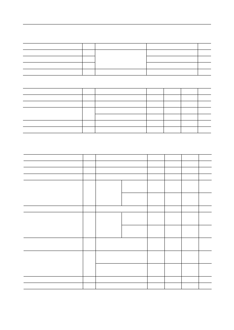
ABSOLUTE MAXIMUM RATINGS
Parameter
Power Supply Voltage
Input Voltage
Power Dissipation
Storage Temperature
Symbol
V
DD
V
IN
P
D
T
STG
Condition
Ta = 25∞C
--
Rating
≠0.3 to +7
≠0.3 to V
DD
+ 0.3
1
≠55 to +150
Unit
V
V
W
∞C
RECOMMENDED OPERATING CONDITIONS
Parameter
Power Supply Voltage
Power Supply Voltage
Input High Voltage
Input Low Voltage
Operating Temperature
Symbol
V
DD
V
SS
V
IH
V
IL
Ta
Condition
--
--
Pins other than X1
--
--
Min.
4.5
--
2.4
0
≠40
Unit
V
V
V
V
∞C
Typ.
5
0
--
--
+25
Max.
5.5
--
V
DD
0.8
+85
X1 pin
3.5
V
--
V
DD
ELECTRICAL CHARACTERISTICS
DC Characteristics
(Ta = ≠40∞C to +85∞C)
Min.
Typ.
Max.
Unit
Condition
Symbol
Parameter
4.2
--
V
DD
V
0
--
0.4
V
≠100
≠50
≠10
mA
--
0.1
10
mA
≠100
≠50
+10
mA
--
30
40
mA
--
4
5
mA
--
--
15
pF
--
--
20
pF
--
0.1
10
mA
--
6
8
mA
≠10
≠0.1
--
mA
≠10
≠0.1
--
mA
Output High Voltage
Output Low Voltage
High Level Input Current
Low Level Input Current
High Level Output Current
Low Level Output Current
Power Supply Current
(Operating)
Power Supply Current(Stand-by)
PWDWN="L"
Input Capacitance
Output Load Capacitance
V
OH
V
OL
I
IH
I
IL
I
OZH
I
OZL
I
DDO
I
DDS
C
I
C
LOAD
--
--
When oscillation circuit is
used as basic clock
--
V
OL
=
V
SS
to V
DD
Input other than
the above
PD15 to PD0
with pull-up
V
OH
= V
DD
V
IL
=
V
SS
to V
DD
Input other than
the above
SF1, SF2
with pull-up
I
OH
= 40 mA
I
OL
= 1.6 mA
V
IH
= V
DD
When extarnal input is used
as basic clock
° Semiconductor
MSM7620
11/28
Echo Canceler Characteristics (Refer to Characteristics Diagram)
R
IN
= ≠10 dBm0
(5 kHz band white noise)
E. R. L. (echo return loss)
= 6 dB
T
D
= 20 ms
ATT, GC, NLP: OFF
R
IN
= ≠10 dBm0
(5 kHz band white noise)
E.R.L. = 6 dB
ATT, GC, NLP: OFF
Cancelable Echo Delay Time for a
Slave Chip in a Cascade
Cancelable Echo Delay Time for a
Single Chip or a Master Chip in a
Cascade
Echo Attenuation
Parameter
Symbol
Condition
L
RES
T
D
T
DS
Min.
Typ.
Max.
Unit
--
30
--
dB
--
--
23
ms
--
--
31
ms

° Semiconductor
MSM7620
12/28
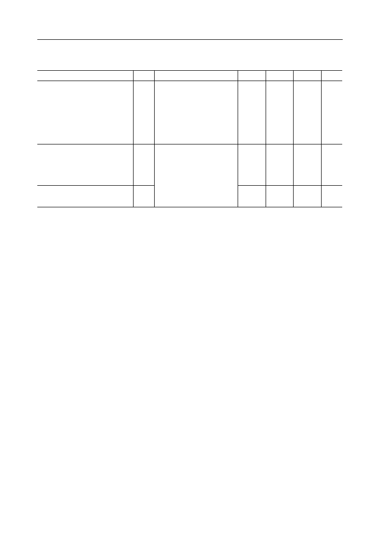
AC Characteristics
(Ta = ≠40∞C to +85∞C)
Parameter
Clock Frequency
Clock Cycle Time
Clock Duty Ratio
Clock "H" Level Pulse Width
Clock "L" Level Pulse Width
Clock Rise Time
Clock Fall Time
Sync Clock Output Time
Internal Sync Clock Frequency
Internal Sync Clock Output Cycle Time
Internal Sync Clock Duty Ratio
Internal Sync Signal Output Delay Time
Internal Sync Signal Period
Internal Sync Signal Output Width
Transmit/receive Operation Clock Frequency
Transmit/receive Sync Clock Cycle Time
Transmit/receive Sync Clock Duty Ratio
Transmit/receive Sync Signal Period
Sync Timing
Sync Signal Width
Receive Signal Setup Time
Receive Data Input Time
IRLD Signal Output Delay Time
IRLD Signal Output Width
Serial Output Delay Time
--
--
--
--
--
--
--
--
f
c
= 18 MHz
f
c
= 18 MHz
f
c
= 18 MHz
f
c
= 18 MHz
f
c
= 18 MHz
--
--
--
--
--
--
--
--
--
--
--
--
--
Symbol
Condition
f
C
t
MCK
t
DMC
t
MCH
t
MCL
t
r
t
f
t
DCM
f
CO
t
CO
t
DCO
t
DCC
t
CYO
t
WSO
f
SCK
t
SCK
t
DSC
t
CYC
t
XS
t
SX
t
WSY
t
DS
t
ID
t
DIC
t
WIR
t
SD
t
XD
Min.
17.5
54.1
40
23.5
23.5
--
--
--
--
--
--
--
--
--
--
--
--
--
--
64
0.488
40
123
45
45
t
SCK
45
Typ.
18.0
55.56
50
--
--
--
--
--
200
5
50
--
125
t
CO
--
--
--
--
--
--
50
125
--
--
--
7t
SCK
t
SCK
Max.
18.5
57.1
60
--
--
--
--
--
--
--
--
5
5
100
5
2048
15.6
60
t
CYC
≠t
SCK
138
90
90
--
--
--
--
--
--
Unit
MHz
ns
%
ns
ns
ns
ns
ns
kHz
ms
%
ns
ms
ms
kHz
ms
%
ms
ns
ns
ms
ns
ms
ns
ms
ns
f
c
= 18 MHz
Receive Data Hold Time
--
t
DH
45
--
--
ns
° Semiconductor
MSM7620
13/28
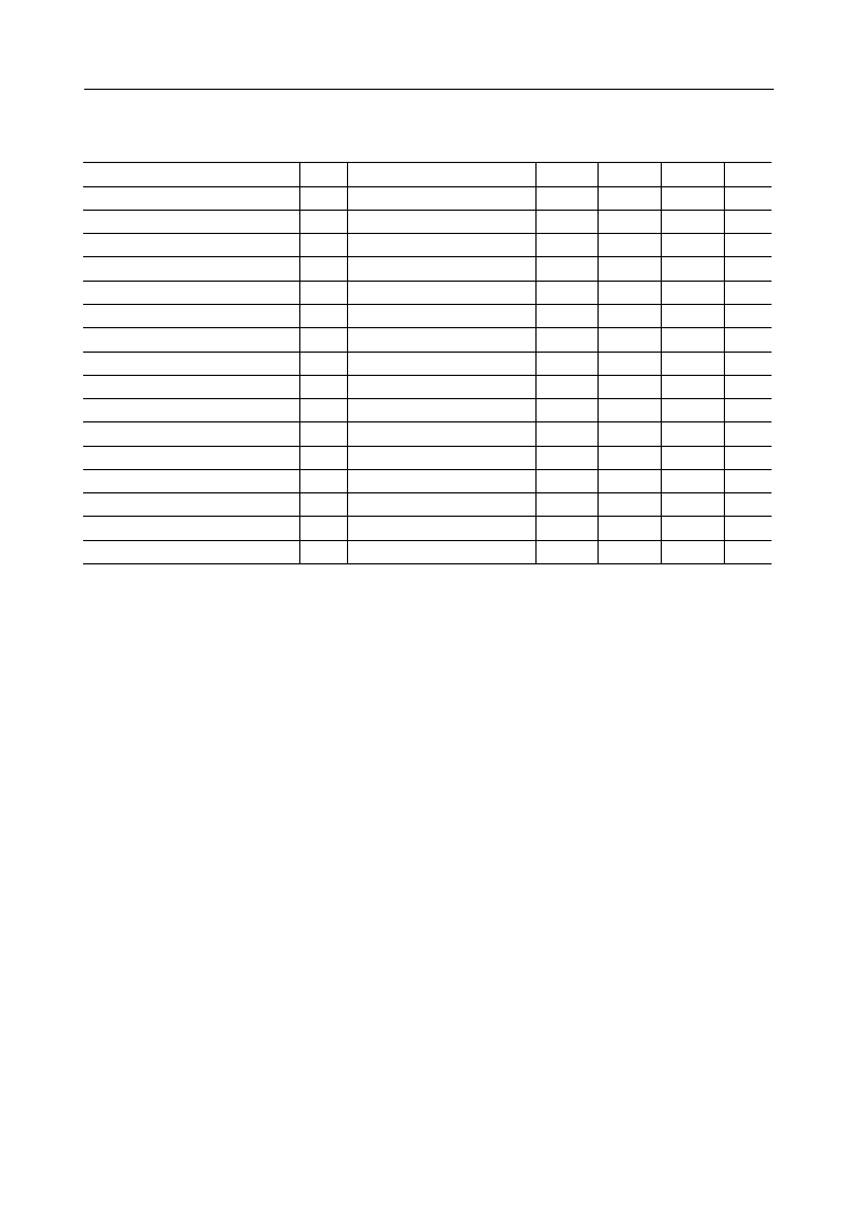
AC Characteristics (Continued)
(Ta = ≠40∞C to +85∞C)
Parameter
Symbol
Condition
Min.
Typ.
Max.
Unit
t
WR
--
1
--
--
ms
t
DRS
--
5
--
--
ns
t
DRE
--
--
--
52
ns
t
DIT
--
100
--
--
ms
t
DPS
--
--
--
111
ns
t
DPE
--
--
--
15
ns
t
DTS
--
20
--
--
ns
t
DTH
--
120
--
--
ns
t
DSR
--
20
--
--
ns
t
DHR
--
10
--
--
ns
t
WPD
--
--
2t
MCK
--
ns
t
DF
--
--
t
MCK
--
ns
t
WFO
--
--
t
MCK
/2
--
ns
t
WFI
OFz connected to SFx
--
t
WFO
--
ns
t
FS
--
--
20
--
ns
t
FH
--
--
10
--
ns
Reset Signal Input Width
Reset Start Time
Reset End Time
Processing Operation Start Time
Power Down Start Time
Power Down End Time
Control Pin Setup Time (
INT)
Control Pin Hold Time (
INT)
Control Pin Setup Time (
RST)
Control Pin Hold Time (
RST)
Parallel Data Output Signal Width
Flag Signal Output Time
Flag Signal Output Width
Flag Signal Input Width
Data Read Setup Time
Data Read Hold Time
° Semiconductor
MSM7620
14/28
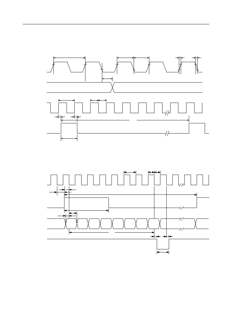
TIMING DIAGRAM
Clock Timing
t
r
t
f
t
MCH
t
MCL
fc. t
MCK
X1/CLKIN
t
DCM
SCKO
SCKO
SYNCO
fco. t
CO
t
DCO
t
DCC
t
DCC
t
CYO
t
WSO
t
DMC
Serial Input Timing
SCK
SYNC
SIN
RIN
MSB
MSB
t
CYC
fsck. t
SCK
t
SX
t
XS
t
WSY
t
DS
t
DH
t
DSC
7
7
6
5
4
3
2
1
LSB
0
t
ID
t
DIC
t
DIC
IRLD
t
WIR
° Semiconductor
MSM7620
15/28
Serial Output Timing
SCK
SYNC
SOUT
ROUT
MSB
MSB
t
CYC
fsck. t
SCK
t
SX
t
XS
t
WSY
t
SD
t
DSC
7
7
6
5
4
3
2
1
LSB
0
t
XD
t
XD
High-Z
High-Z
t
XD
Operation Timing After Reset
RST
Internal operation
,
t
WR
t
DRS
*Reset timing can be asynchronous
Processing Start
,
t
DIT
Reset
Initialization
t
DRE
Note:
INT is invalid in the diagonally shaded interval.
Power Down Timing
PWDWN
Internal Operation
,,
*t
DPS
Processing Start
Power Down
t
DPE
*Input MCK in the t
DPS
interval.
° Semiconductor
MSM7620
16/28
Control Pin Load-in Timing
INT(IRLD)
*t
CYC
NLP, HCL,
ATT, ADP, GC
t
DHR
RST
t
WR
t
DSR
NLP, HCL,
ATT, ADP, GC
t
DTH
t
DTS
*Refer to the Serial Input Timing
Parallel Output Timing
PD15
PD 0
Output Data
t
WPD
t
WFO
OF1
OF2
≠
t
DF
High-Z
High-Z
Parallel Input Timing
Input Data
t
FS
t
FH
t
WFI
SF1
SF2
PD15
PD 0
≠
° Semiconductor
MSM7620
17/28
HOW TO USE THE MSM7620
The MSM7620 cancels the echo which returns to SIN using the RIN signal.
Connect the base signal to the R-side and the echo generated signal to the S-side.
Connection Methods According to Echos
Example 1:
Canceling acoustic echo (to handle acoustic echo from line input)
Acoustic echo
CODEC
MSM7620
CODEC
m-law
m-law
ROUT
RIN
SIN
SOUT
Line input
H
AFF
+
≠
+
Example 2:
Canceling line echo (to handle line echo from microphone input)
Example 3:
Canceling line echo in a cascade connection
(to handle line echo from microphone input)
CODEC
MSM7620
CODEC
m-law
m-law
ROUT
RIN
SIN
SOUT
Line echo
H
AFF
+
≠
+
Microphone Input
CODEC
MSM7620
CODEC
m-law
m-law
ROUT
RIN
SIN
SOUT
Line echo
H
AFF
+
≠
+
Microphone input
Master
H
AFF
Slave
PD0 - 15
° Semiconductor
MSM7620
18/28
Example 4: Canceling of both acoustic echo and line echo
(to handle both acoustic echo from line input and line echo from microphone input)
Acoustic echo
CODEC
MSM7620
CODEC
m-law
m-law
ROUT
RIN
SIN
ROUT
Line input
H
AFF
+
≠
+
AFF
+
≠
+
SOUT
SIN
RIN
SOUT
Line echo
Microphone input
For line echo
For acoustic echo
MSM7620
° Semiconductor
MSM7620
19/28
Control Pin Connection Example
Single Chip Connection
NLP
HCL
ADP
ATT
GC
PWDWN
RST
NLP
HCL
ADP
ATT
GC
PWDWN
RST
INT
SF1 *
SF2 *
MS *
≠
*
PD 0
IRLD
*
OF1
*
OF2
*
PD15
+5 V
Asterisk * mark indicates a pin only for the MSM7620-011.
NLP
HCL
ADP
ATT
GC
PWDWN
RST
NLP
HCL
ADP
ATT
GC
PWDWN
RST
INT
SF1
SF2
MS
≠
PD 0
IRLD
OF1
OF2
PD15
+5 V
Master chip
NLP
HCL
ADP
ATT
GC
PWDWN
RST
INT
SF1
SF2
MS
≠
PD 0
IRLD
OF1
OF2
PD15
Slave chip
+5 V
Four-stage Cascade Connection
Master + (slave • 3)
NLP
HCL
ADP
ATT
GC
PWDWN
RST
NLP
HCL
ADP
ATT
GC
PWDWN
RST
INT
SF1
SF2
MS
≠
PD 0
IRLD
OF1
OF2
PD15
+5 V
Master chip
NLP
HCL
ADP
ATT
GC
PWDWN
RST
INT
SF1
SF2
MS
≠
PD 0
IRLD
OF1
OF2
PD15
Slave chip 1
+5 V
NLP
HCL
ADP
ATT
GC
PWDWN
RST
INT
SF1
SF2
MS
≠
PD 0
IRLD
OF1
OF2
PD15
Slave chip 2
+5 V
NLP
HCL
ADP
ATT
GC
PWDWN
RST
INT
SF1
SF2
MS
≠
PD 0
IRLD
OF1
OF2
PD15
Slave chip 3
+5 V
Two-stage Cascade Connection
Master + (slave • 1)

° Semiconductor
MSM7620
20/28
Clock Circuit Example
Internal clock generator circuit
MSM7620
X1/CLKIN
X2
XTAL
R
C1
C2
R
XTAL
C1
C2
GND
GND
: 18 MHz
: 1 MW
: 27 pF
: 27 pF
External clock input circuit
MSM7602
X1/CLKIN
X2
18 MHz
5pF
GND
° Semiconductor
MSM7620
21/28
ECHO CANCELER CHARACTERISTICS DIAGRAM
0
10
20
30
40
40
30
20
10
0
ERL vs. echo attenuation
Echo attenuation [dB]
ERL. [dB]
Measurement Conditions
RIN input = ≠10 dBm 5 kHz band white noise
(0 dBm = 2.2 dBm0)
Echo delay time T
D
= 20 ms
ATT, GC, NLP = OFF
0
10
20
30
40
≠50 ≠40 ≠30 ≠20 ≠10
0
RIN input level vs. echo attenuation
Echo attenuation [dB]
RIN input level [dBm]
0 dBm = 2.2 dBm0
Measurement Conditions
RIN input: 5 kHz band white noise
Echo delay time T
D
= 20 ms
ERL = 6 dB
ATT, GC, NLP = OFF
0
10
20
30
0
Echo delay time vs. echo attenuation
Echo attenuation [dB]
Echo delay time [ms]
200
150
100
50
Measurement Conditions
RIN input = ≠10 dBm
5 kHz band white noise
(0 dBm = 2.2 dBm0)
1
2
3
4
5
6
7chip
ERL = 6 dB
ATT, GC, NLP = OFF
The second through seventh chips
are connected in a cascade.
≠10
° Semiconductor
MSM7620
22/28
Measurement System Block Diagram
m-law
ROUT
RIN
SIN
SOUT
CODEC
RIN input
White noise generator
Level meter
Delay
ATT
T
D
Echo delay time
L. P. F.
5 kHz
A
A
PCM
PCM
m-law
CODEC
A
A
PCM
PCM
ERL
(echo return loss)
MSM7543
MSM7543
MSM7620
° Semiconductor
MSM7620
23/28
APPLICATION CIRCUIT
Bidirectional Connection Example
SOUT
RIN
NLP
HCL
ADP
ATT
GC
V
DD
V
SS
SIN
ROUT
SCK
SYNC
INT
IRLD
PWDWN
RST
WDT
9
14
11
12
7
8
23
27
28
13
10
2
3
4
6
29
32
5
MSM7543GS-VK
PCMOUT
PCMIN
AIN+
VFRO
GSX
SG
SGC
23
6
21
1
13
12
SIN
C1
R2
R3
R1
AIN≠
22
BCLOCK
15
RSYNC
11
PDN
10
TMC
19
ROUT
R5
R4
R6
CLK
EXT.
SCK
EXT.
SYNC
RST
PWDWN
Mike input
Speaker output
V
DD
AG
XSYNC
14
DG
9
SYNCO
24
SCKO
25
X1
20
X2
21
V
SS
16
C4
+ +
13
10
2
3
4
6
29
32
5
16
C8
SOUT
RIN
NLP
HCL
ADP
ATT
GC
V
DD
V
SS
V
SS
MSM7620-001GS-K
R12
SIN
ROUT
SCK
SYNC
INT
IRLD
PWDWN
RST
WDT
SYNCO
SCKO
X1
X2
9
14
11
12
7
8
23
27
28
24
25
20
21
13
12
15
11
10
19
14
9
PCMOUT
PCMIN
BCLOCK
RSYNC
PDN
TMC
XSYNC
DG
AIN+
VFRO
GSX
SG
SGC
AIN≠
V
DD
AG
MSM7543GS-VK
23
6
21
1
24
22
16
R10
R11
C5
R8
R9
R7
RIN
SOUT
Circuit input
Circuit output
R8 > 20 kW
R9 > 20 kW
R10 = 2.2 kW
R11 = 10 kW
R12 = 10 kW
R13 = 0-22 W
R14 = 0-22 W
C6 = 10 mF
C7 = 0.1 mF
C8 = 10 mF
C9 = 1.0 mF
C10 = 1.0 mF
R1 > 50 kW
R2 > 20 kW
R3 > 20 kW
R4 = 2.2 kW
R5 = 10 kW
R6 = 10 kW
R7 > 50 kW
C1 = 0.1 mF
C2 = 10 mF
C3 = 0.1 mF
C4 = 10 mF
C5 = 0.1 mF
8
For cancellation of line echo
32-Pin SSOP
For cancellation of acoustic echo
32-Pin SSOP
MSM7620-001GS-K
3
5
AOUT≠
PWI
3
5
AOUT≠
PWI
24
16
8
+
C7
C6
C10
R13
C2
+
C9
R14
C3

° Semiconductor
MSM7620
24/28
Cascade Connection Example
14
11
52
51
34
33
30
29
28
27
26
25
24
23
22
21
20
19
60
54
55
59
6
8
45
13
12
15
11
14
10
19
10
15
12
13
44
38
1
2
3
4
5
46
41
40
35
36
47
48
62
16
SIN
ROUT
SCK
SYNC
RST
PWDWN
NLP
HCL
ADP
MS
ATT
GC
SCKO
SYNCO
X1
X2
V
DD
V
DD
V
DD
V
SS
SOUT
RIN
PD15
PD14
PD13
PD12
PD11
PD10
PD 9
PD 8
PD 7
PD 6
PD 5
PD 4
PD 3
PD 2
PD 1
PD 0
OF2
SF2
OF1
SF1
INT
IRLD
WDT
SIN
ROUT
SCK
SYNC
RST
PWDWN
NLP
HCL
ADP
MS
ATT
GC
SCKO
SYNCO
X1
X2
V
DD
V
DD
V
DD
V
SS
SOUT
RIN
PD15
PD14
PD13
PD12
PD11
PD10
PD 9
PD 8
PD 7
PD 6
PD 5
PD 4
PD 3
PD 2
PD 1
PD 0
OF2
SF2
OF1
SF1
INT
IRLD
WDT
14
11
52
51
34
33
30
29
28
27
26
25
24
23
22
21
20
19
60
54
55
59
6
8
45
13
12
15
11
14
10
19
10
15
12
13
44
38
1
2
3
4
5
46
41
40
35
36
47
48
62
16
23
6
21
22
1
PCMOUT
PCMIN
BCLOCK
RSYNC
XSYNC
PDM
TMC
PCMOUT
PCMIN
BCLOCK
RSYNC
XSYNC
PDM
TMC
AIN +
MSM7543GS-VK
MSM7543GS-VK
Master
Slave
R1
R2
R3
C1
SIN
ROUT
R4
R5
9
DG
+
C4
64-Pin QFP
64-Pin QFP
RST
PWDWN
+
C8
RIN
SOUT
R7
R8
R6
R7 > 20 k
W
R8 > 20 k
W
R9 = 2.2 k
W
R10 = 10 k
W
R11 = 0-22
W
R12 = 0-22
W
C6 = 10
m
F
C7 = 0.1
m
F
C8 = 10
m
F
C9 = 1.0
m
F
C10 = 1.0
m
F
R1 > 50 k
W
R2 > 20 k
W
R3 > 20 k
W
R4 = 2.2 k
W
R5 = 10 k
W
R6 > 50 k
W
C1 = 0.1
m
F
C2 = 10
m
F
C3 = 0.1
m
F
C4 = 10
m
F
C5 = 0.1
m
F
DG
R9
R10
C5
9
MSM7620-011GS-BK
MSM7620-011GS-BK
CLK
23
6
21
22
1
24
VFRO
GSX
AIN≠
SG
SGC
V
DD
AG
5
3
AOUT≠
PWI
AIN +
VFRO
GSX
AIN≠
SG
SGC
V
DD
AG
24
5
3
AOUT≠
PWI
16
8
16
8
+
C7
C6
C10
R12
C2
+
C9
R12
C3

° Semiconductor
MSM7620
25/28
NOTES ON USE
1. Set echo return loss (ERL) to be attenuated. If the echo return loss is set to be
amplified, the echo can not be eliminated.
Refer to the characteristics diagram for ERL vs. echo attenuation quantity.
2. Set the level of the analog input so that the PCM CODEC does not overflow.
3. The recommended input level is ≠10 to ≠20 dBm0. Refer to the characteristics
diagram for the RIN input level vs. echo attenuation quantity.
4. Applying the tone signal to this echo canceler will decrease echo attenuation. If the
tone signal is input to the SIN pin during the time that a signal is input to the RIN
pin, this echo cancceler operates faultily.
A signal must be input to either the RIN pin or the SIN pin. The ADP or HCL pin
must be driven at "H" if the tone signal is input to the SIN pin during the time that
a signal is input to the RIN pin.
5. For changes in the echo path (retransmit, circuit switching during transmission, and
so on), convergence may be difficult.
Perform a reset to make it converge.
If the state of the echo path changes after a reset, convergence may again be difficult.
In cases such as a change in the echo path, perform a reset when possible.
6. When turning the power ON, set the PWDWN pin to "1" and input the basic clock
simultaneouly with power ON.
If powering down immediately after power ON, be sure first input 10 or more clocks
of the basic clock.
7. After powering ON, be sure to reset.
8. After the power down pin is changed to a "1" from a "0", be sure to reset.
9. If this canceler is used to cancel acoustic echoes, an echo attenuation may be less
than 30 dB.

° Semiconductor
MSM7620
26/28
EXPLANATION OF TERMS
Attenuating Function :
This function prevents howling and controls the noise level with an
attenuator for the RIN input and SOUT output. Refer to the
explanation of pins (ATT pin).
Echo Attenuation :
If there is talking (input only to RIN) in the path of a rising echo
arises, the echo attenuation refers to the difference in the echo
return loss (canceled amount) when the echo canceler is not used
and when it is used.
Echo attenuation = (SOUT level during through mode operation)
≠ (SOUT level during echo canceler operation) [dB]
Echo Delay Time :
This is the time from when the signal is output from ROUT until it
returns to SIN as an echo or other similar device.
Acoustic Echo :
When using a hands free phone, and so on, the signal output from
the speaker echoes and is input again to the microphone. The
return signal is referred to as acoustic echo.
Telephone Line Echo :
This is a signal which is delayed midway in a telephone line and
returns as an echo, due to reasons such as a hybrid impedance
mismatch.
Gain Control Function :
This function prevents howling and controls the sound level by
with a gain controller for the RIN input. Refer to the explanation
of pins (GC pin).
Center Clipping Function : This function forces the SOUT output to a minimum value when
the signal is below ≠57 dBm0. Refer to the explanation of pins (NLP
pin).
Double Talk Detection :
Double talk refers to a state in which the SIN and RIN signals are
input simultaneously. In a double talk state, a signal outside the
echo signal which is to be canceled can be input to the SIN input,
resulting in misoperation.
The double talk detector prevents such misoperations of the canceler.
Howling Detection :
This is the oscillating state caused by the acoustic coupling between
the loud speaker and the microphone during hands free talking.
Howling not only interferes with talking, but can also cause
misoperation of the echo canceler.
The howling detector prevents such misoperation and prevents
howling.
Echo Return Loss (ERL) :
When the signal output from ROUT returns to SIN as an echo, ERL
refers to how much loss there is in the signal level during ROUT.
ERL = (ROUT level) ≠ (SIN level of the ROUT signal which returns
as an echo) [dB]
If ERL is positive (ROUT > SIN), the system is an attenuator system.
If ERL is negative (ROUT < SIN), the system is an amplifier system.
° Semiconductor
MSM7620
27/28
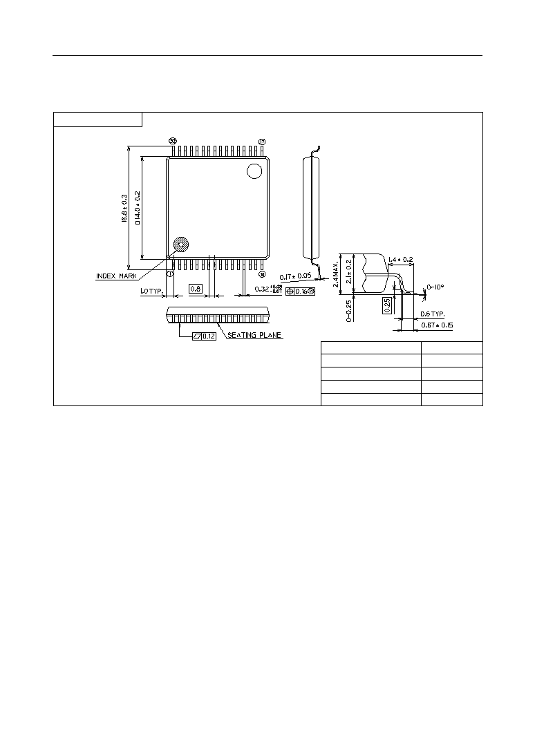
(Unit : mm)
PACKAGE DIMENSIONS
Notes for Mounting the Surface Mount Type Package
The SOP, QFP, TSOP, SOJ, QFJ (PLCC), SHP and BGA are surface mount type packages, which
are very susceptible to heat in reflow mounting and humidity absorbed in storage.
Therefore, before you perform reflow mounting, contact Oki's responsible sales person for the
product name, package name, pin number, package code and desired mounting conditions
(reflow method, temperature and times).
Package material
Lead frame material
Pin treatment
Solder plate thickness
Package weight (g)
Epoxy resin
42 alloy
Solder plating
5 mm or more
0.83 TYP.
SSOP32-P-640-0.80-K
Mirror finish
° Semiconductor
MSM7620
28/28
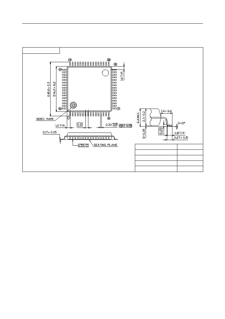
(Unit : mm)
Notes for Mounting the Surface Mount Type Package
The SOP, QFP, TSOP, SOJ, QFJ (PLCC), SHP and BGA are surface mount type packages, which
are very susceptible to heat in reflow mounting and humidity absorbed in storage.
Therefore, before you perform reflow mounting, contact Oki's responsible sales person for the
product name, package name, pin number, package code and desired mounting conditions
(reflow method, temperature and times).
QFP64-P-1414-0.80-BK
Package material
Lead frame material
Pin treatment
Solder plate thickness
Package weight (g)
Epoxy resin
42 alloy
Solder plating
5 mm or more
0.87 TYP.
Mirror finish