
° Semiconductor
MSM7653
1/35
° Semiconductor
MSM7653
NTSC/PAL Digital Video Encoder
GENERAL DESCRIPTION
The MSM7653 is a digital NTSC/PAL encoder. By inputting digital image data conforming to
ITU Rec. 656 or ITURBT 601, it outputs selected analog composite video signals, analog S video
signals. For the scanning system, interlaced or noninterlaced mode can be selected.
Since the MSM7653 is provided with pins dedicated to overlay function, text and graphics can
be superimposed on a video signal.
In addition, this encoder has an internal 10-bit DAC. So, when compared with using a conventional
analog encoder, the number of components, the board space, and points of adjustment can
greatly be reduced, thereby realizing a low cost and high-accuracy system.
The MSM7653 provides the optional functions such as Macrovision Rev. 7.01 (note 1) (note 2) and
Closed Caption Signal Generation Function.
The host interface provided conforms to Philips's I
2
C specifications, which reduces
interconnections between this encoder and mounting components.
The internal synchronization signal generator (SSG) allows the MSM7653 to operate in master
mode.
FEATURES
∑ Video signal system: NTSC/PAL
∑ Scanning system: interlaced/noninterlaced (NTSC : 262 lines/PAL : 312 lines)
∑ Input digital level: conforms to ITU-R601 (CCIR601)
∑ Input-output timing: conforms to ITU Rec. 656 or ITURBT 624-4
∑ Input signal sampling ratio : Y:Cb:Cr = 4:2:2
∑ Supported input formats
∑ ITU Rec. 656
∑ YCbCr 27 MHz format (8-bit input)
∑ ITU-R601 13.5 MHz (8-bit (Y) + 8-bit (CbCr) input)
∑ Sampling frequency : 27 MHz
∑ Internal SSG circuit (Can operate as a master in other operation modes than CCIR Rec. 656
mode)
∑ Internal 3ch 10-bit DAC
∑ 3-bit title graphics can be displayed
∑ Color bar function
∑ I
2
C-bus host interface function
∑ 3.3 V single power supply (each I/O pin is 5 V tolerable)
∑ Closed caption function
∑ Macrovision Rev. 7.01
∑ Package
56-pin plastic QFP (QFP56-P-910-0.65-2K)
(Product name: MSM7653GS-2K)
E2F0026-29-63
This version: Jun. 1999
Previous version: Jun. 1998

° Semiconductor
MSM7653
2/35
APPLICATIONS
∑ Set top box
∑ DVD
∑ Digital VTR
(Note 1) This device is protected by U.S. Patent numbers 4631603, 4577216 and 4819098 and
other intellectual property rights. The use of Macrovision Corporation's copy protection
technology in the device must be authorized by Macrovision and is intended for home
and other limited pay-per-view uses only, unless otherwise authorized in writing by
Macrovision. Reverse engineering or disassembly is prohibited.
(Note 2) This data sheet does not describe the register setting method of implementing
Macrovision Corporation's anticopy function that this device provides.
Refer to MACROVISION ANTICOPY FUNCTION SETTING MANUAL for the
anticopy function.
° Semiconductor
MSM7653
3/35
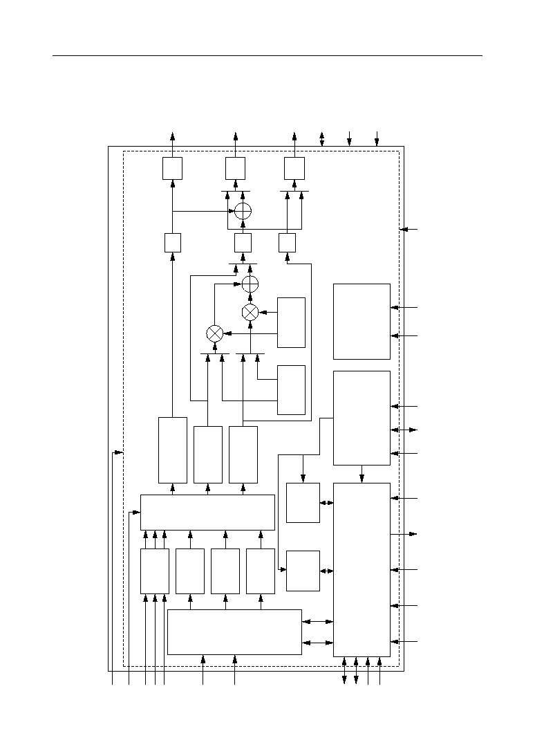
BLOCK DIAGRAM
Sync Generator & Timing Controller
Prologue
Block
I
2
C Control logic
Test Control logic
IPF
Overlay
Control
YUV color
Generator
RESET_L
Black &
Blank Pedestal
Interpolator
+ LPF
Interpolator
+ LPF
Color Burst
Generator
Y Level
converter
U Level
converter
V Level
converter
Anticopy
Function
Block
Closed
Caption
Block
OLC
OLG
OLB
CD[7:0]
CLKX2
MODE
CLKX1O CLKSEL
SCL SDA ADRS
Subcarrier
Generator
TENB TEST1
CVBSO
MS
SEL[2:1]
BLANK_L
HSYNC_L
VSYNC_L
YD[7:0]
OLR
DAC
IPF
YA
DAC
IPF
IPF = Interpolation Filter
CA
DAC
VREF
FS
OUTSEL
COMP
° Semiconductor
MSM7653
4/35
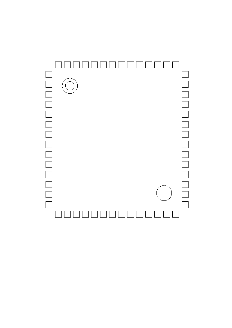
PIN CONFIGURATION (TOP VIEW)
NC : No-connection pin
56-Pin Plastic QFP
1
56
55
54
53
52
51
50
49
48
47
46
45
44
43
15
16
17
18
19
20
21
22
23
24
25
26
27
28
DGND
TEST1
TENB
VREF
FS
COMP
AGND
CA
AV
DD
CVBSO
AGND
YA
AV
DD
DGND
DGND
YD0
YD1
YD2
YD3
YD4
YD5
NC
YD6
YD7
BLANK_L
HSYNC_L
VSYNC_L
DGND
2
3
4
5
6
7
8
9
10
11
12
13
14
42
41
40
39
38
37
36
35
34
33
32
31
30
29
DV
DD
MS
SDA
SCL
ADRS
RESET_L
MODE
OLC
OLR
OLG
OLB
CLKX1O
OUTSEL
DV
DD
DV
DD
SEL2
SEL1
CLKSEL
CD0
CD1
CD2
CD3
CD4
CD5
CD6
CD7
CLKX2
DV
DD
° Semiconductor
MSM7653
5/35
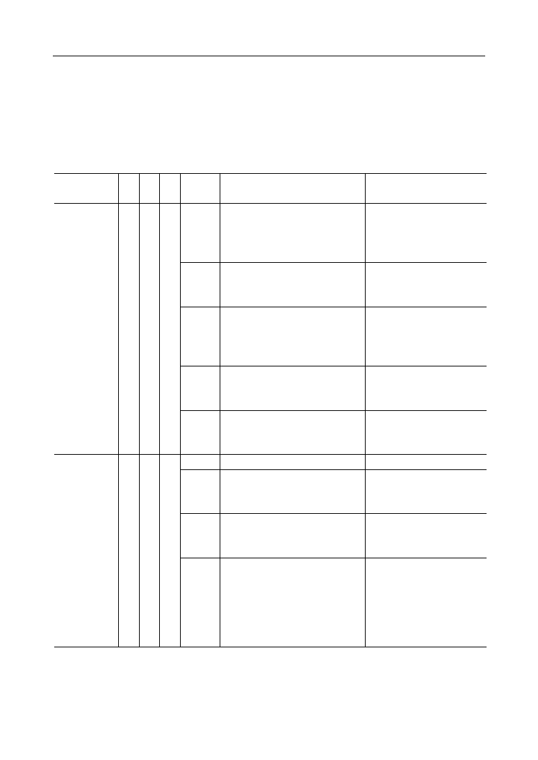
PIN DESCRIPTIONS (1/2)
Pin
I/O
Symbol
Description
1
DV
DD
3.3 V digital power supply
2
I
MS
Selects between Master and Slave at 27 MHz or 13.5 MHz YCbCr operation. Pulled down
3
I/O
SDA
I
2
C interface data bus
4
I
SCL
I
2
C interface clock bus
5
I
ADRS
I
2
C-bus Slave address setting pin ("0" : 1001100 / "1" : 1001110).
Pulled down
6
I
RESET_L
System reset signal. Negative porality
7
I
MODE
Broadcasting mode select pin. "0" : NTSC/"1" : PAL. Pulled down
8
I
OLC
Transparent control signal. "1" indicates overlay signal. Normally fixed to "0".
9
I
OLR
Overlay text color (Red component). Normally fixed to "0".
10
I
OLG
Overlay text color (Green component). Normally fixed to "0".
11
I
OLB
Overlay text color (Blue component). Normally fixed to "0".
12
O
CLKX1O
13.5 MHz divided clock output signal
13
I
OUTSEL
Normally fixed to "0". Pulled down
14
DV
DD
3.3 V digital power supply
15
DGND
Digital GND
16
I/O
VSYNC_L
Vertical sync signal input/output pin (ITU656: O, YCbCr: I/O)
Negative polarity
17
I/O
HSYNC_L
Horizontal signal input/output pin (ITU656 : O, YCbCr: I/O)
Negative polarity
18
I
BLANK_L
Composite blank signal. Negative polarity. See the description on page 15
for the operating requirement.
19, 20
I
YD7 to YD6
MSB 2 bits of 8-bit digital image data input pins (for ITU656 and
YCbCr 27 MHz). Level conforms to ITU-601.
MSB 2 bits of 8-bit digital image luminance signal input pins (for YCbCr).
Level conforms to ITU-601.
YD7 is MSB.
21
NC
Not connected
22 to 27
I
YD5 to YD0
LSB 6 bits of 8-bit digital image data input pins (for ITU656 and
YCbCr 27 MHz). Level conforms to ITU-601.
LSB 6 bits of 8-bit digital image luminance signal input pins (for YCbCr).
Level conforms to ITU-601.
YD0 is LSB.
28
DGND
Digital GND
29
DV
DD
3.3 V digital power supply
30
I
CLKX2
Clock input pin (27 MHz)
31 to 38
I/O
CD7 to CD0
8bit digital image chrominance signal data input pins (13.5 MHz mode).
Level conforms to ITU-601. Fixed to "0" for ITU Rec. 656, 27 MHz-YCbCr mode.
39
I
CLKSEL
Operation mode select pin. "0" : 27 MHz mode / "1" : 13.5 MHz mode.
° Semiconductor
MSM7653
6/35
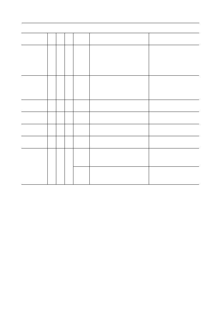
PIN DESCRIPTIONS (2/2)
47
I
FS
DAC full scale adjustment pin.
48
I
COMP
DAC phase complement pin.
49
AGND
Analog GND
50
O
CA
Analog color chrominance signal output pin.
51
AV
DD
3.3 V analog power supply
52
O
CVBSO
Analog composite signal output pin.
53
AGND
Analog GND
54
O
YA
Analog luminance signal output pin.
55
AV
DD
3.3 V analog power supply
56
DGND
Digital GND
43
DGND
Digital GND
44
I
TEST1
Input pin1 for testing. Normally fixed to "0". (See Page 32 for details)
Pulled down
45
I
TENB
Input pin2 for testing. Normally fixed to "0".
Pulled down
46
I/O
VREF
Reference voltage for DAC
42
DV
DD
3.3 V digital power supply
41
I
SEL2
Interface select pin. ITU656 : "0", YCbCr 27 MHz : "1" (See Page 32 for details)
Pulled down
Pin
I/O
Symbol
Description
40
I
SEL1
Enable pin. Normally fixed to "0". Sleep mode "1" with TEST1 = "0"
(See Page 32 for details)
° Semiconductor
MSM7653
7/35
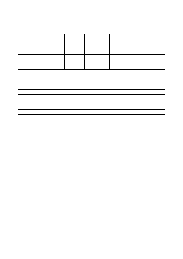
ABSOLUTE MAXIMUM RATINGS
Parameter
Power Supply Voltage
Input Voltage
Analog Output Current
Power Consumption
Storage Temperature
Symbol
DV
DD
AV
DD
V
I
I
O
P
W
T
STG
Condition
--
--
DV
DD
= 3.3 V
--
--
--
Rating
≠0.3 to +4.5
≠0.3 to +4.5
≠0.3 to +5.5
50
600
≠55 to +150
Unit
V
V
mA
mW
∞C
RECOMMENDED OPERATING CONDITIONS
Parameter
Power Supply Voltage (*1)
"L" Level Input Voltage
Symbol
DV
DD
AV
DD
V
IH
V
IL
Condition
--
--
--
--
Typ.
3.3
3.3
--
--
Unit
V
V
V
Operating Temperature 1
Ta
1
DV
DD
= AV
DD
= 3.3 V
25
∞C
Min.
3.0
3.0
2.2
--
0
Max.
3.6
3.6
--
0.8
70
External Reference Voltage
Vrefex
DV
DD
= AV
DD
= 3.3 V,
Ta = 25∞C
1.25
V
--
--
DA Current Setting Resistance
Riadj
(*2)
385
W
--
--
DA Output Load Resistance
R
L
(*3)
75
W
--
--
"H" Level Input Voltage
Operating Temperature 2
Ta
2
DV
DD
= AV
DD
= 3.3 V
DA output load = 37.5 W
25
∞C
0
65
(*1)
Supply an equal voltage to both DV
DD
and AV
DD
.
(*2)
A volume control resistor of approx. 500 W is recommendable for adjusting the output
current. When a DA converter analog output is terminated with a 37.5 W load, Riadj
= approx. 192 W.
(*3)
Indicates the value when Riadj = 385 W (typical value).
° Semiconductor
MSM7653
8/35
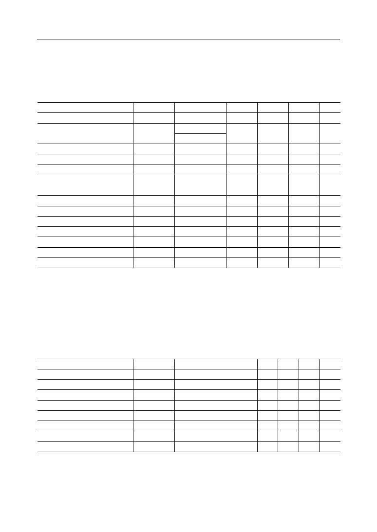
ELECTRICAL CHARACTERISTICS
DC Characteristics
Parameter
Symbol
V
OH
Condition
I
OH
= ≠4 mA (*1)
I
OL
= 4 mA (*1)
Typ.
--
Unit
"L" Level Output Voltage
V
OL
I
OL
= 6 mA (*2)
--
V
Min.
0.7V
DD
--
Max.
--
0.4
"H" Level Output Voltage
V
Input Leakage Current
I
I
V
I
= GND to DV
DD
--
mA
≠10
+10
Output Leakage Current
I
O
V
I
= GND to DV
DD
(*3)
--
mA
≠10
+10
Power Supply Current (operating)
I
DDO
--
120
mA
--
140
Power Supply Current (standby)
I
DDS
RESET_L = "L"
60
mA
--
65
I
2
C-bus SDA Output Voltage
SDAV
L
Low level, I
OL
= 3 mA
--
V
0
0.4
I
2
C-bus SDA Output Current
SDAI
O
During Acknowledge
--
mA
3
--
(Ta = 0 to 70∞C, DV
DD
= 3.3 V ±0.3 V, AV
DD
= 3.3 V ±0.3 V)
Internal Reference Voltage
Vrefin
--
1.25
V
--
--
DA Output Load Resistance
R
L
--
75
W
Integral Linearity
SINL
--
±2
LSB
Differential Linearity
SDNL
--
±1
LSB
CLKX2 = 0 MHz
Power Supply Current (Sleep mode)
I
DDSM
SEL2 = "H"
0.05
mA
0.03
0.5
(*1)
VSYNC_L, HSYNC_L, CD[7:0]
(*2)
CLKX1O
(*3)
SDA
AC Characteristics
Parameter
Symbol
Condition
Min.
Typ.
Max.
Unit
(Ta = 0 to 70∞C, DV
DD
= 3.3 V ±0.3 V, AV
DD
= 3.3 V ±0.3 V)
CLKX2 Cycle Time
T
S
37.0
ns
Input Data Setup Time
Input Data Hold Time
Output Delay Time
CLKX1O Delay Time
t
s1
t
h1
t
d1
t
d2
7
ns
5
ns
5
25
ns
5
25
ns
I
2
C-bus Clock Cycle Time
t
C_SCL
ns
Rpull_up = 4.7 kW
I
2
C-bus High Level Cycle
t
H_SCL
--
ns
I
2
C-bus Low Level Cycle
t
L_SCL
ns
Rpull_up = 4.7 kW
--
--
--
--
--
--
--
--
100
--
--
--
--
--
200
100
--
Rpull_up = 4.7 kW
--
--
--
--
° Semiconductor
MSM7653
9/35
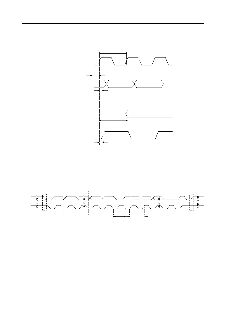
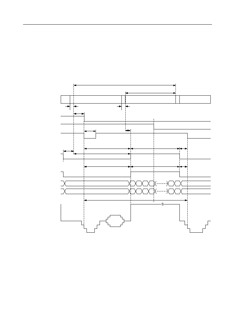
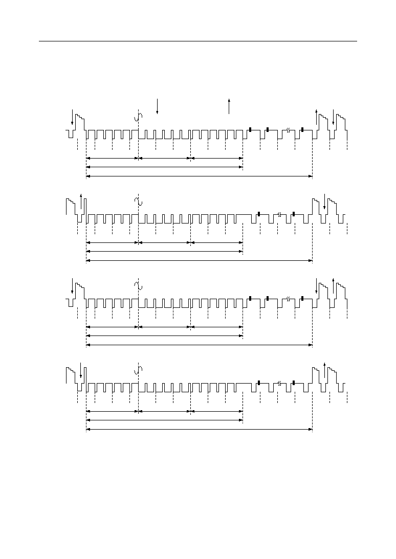
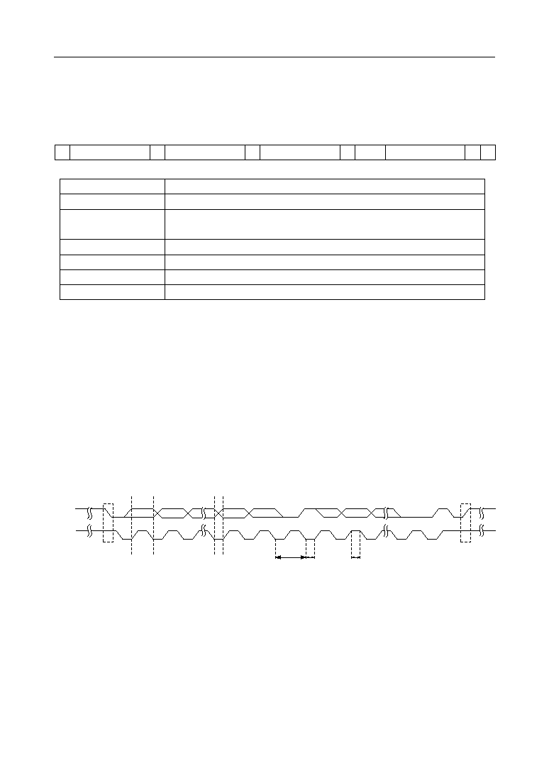
INPUT/OUTPUT TIMING
CLKX2
HSYNC_L,
VSYNC_L, BLANK_L,
YD, CD, MS, MODE,
OLR, OLG, OLB, OLC
HSYNC_L, VSYNC_L
,
CLKX1O
TS
th1
td1
td2
ts1
Invalid data
valid data
Input timing
Output timing
1
2
7
8
9
ACK
1
2
3-8
9
ACK
S
Start Condition
P
Stop Condition
Change of Data Allowed
SCL
SDA
MSB
t
C_SCL
t
L_SCL
Data Line Stable: Data Valid
t
H_SCL
I
2
C-bus Interface Input/Output Timing
The following figure shows I
2
C-bus basic input/output timing.
I
2
C-bus Basic Input/Output Timing

° Semiconductor
MSM7653
10/35
BLOCK FUNCTIONAL DESCRIPTION
1. Prologue Block
This block separates input data at the ITU Rec.656 format into a luminance signal (Y) and a
chrominance signal (Cb & Cr), and also generates information/concerning sync signals
HSYNC_L, VSYNC_L, and BLANK_L.
This block separates input data at the 27 MHz YCbCr (8-bit input) format into a luminance
signal (Y) and a chrominance signal (Cb & Cr).
This block separates input data at the 13.5 MHz YCbCr (16-bit input) format into a chrominance
signal Cb and a chrominance signal Cr.
Of the processed input data, luminance and chrominance signals other than valid pixel data
are replaced by 8'h10 and 8'h80 respectively.
2. Y Limiter Block
This block limits the luminance input signal by clipping the lower limit of an input signal outside
the ITU601 Standard
∑ Signals are limited to YD = 16 when YD < 16.
∑ Signals are limited to TD = 254 when YD (input during a valid pixel period) = 255.
In other cases, signals are fed as is to next processing.
3. C Limiter Block
This block limits the chrominance signal by clipping the upper and lower limits of the input
signal outside the ITU601 Standard.
CD = 1 when CD = 0 is input during a valid pixel period.
CD = 254 when CD = 255 is input during a valid pixel period.
∑ Y Level Converter
Converts ITU-601 standard luminance signal level to DAC digital input level.
∑ U Level Converter
Converts ITU-601 standard chrominance signal level to DAC digital input level.
∑ V Level Converter
Converts ITU-601 standard chrominance signal level to DAC digital input level.
∑ YUV Color Generator
This block generates luminance and chrominance signals from over lay color signals OLR,
OLG and OLB. Control signals (CR [2:0] ) control the output content (overlay or color bar) and
output level (100%, 75%, 50%, 25%).
∑ Overlay Control
This block selects input image data or YUV Color Generator output signals.
It is determined by the level of the control signal (OLC, CR [2]), as shown below: (x : don't care)
CR [2] = 1, OLC = x: Selects color bar signal (YUV Color Generator output signal).
CR [2] = 0, OLC = 1: Selects overlay signal (YUV Color Generator output signal).
CR [2] = 0, OLC = 0: Selects input image data.

° Semiconductor
MSM7653
11/35
∑ Black & Blank Pedestal
This block adds sync signals at the luminance side to luminance signals.
∑ Interpolator + LPF
This block executes data interpolation and the elimination of high frequency components by
LPF for input chrominance signals.
∑ I
2
C Control Logic
This is the serial interface block based on I
2
C standard of Phillips Corporation.
Internal registers MR and CR can be set from the master side.
When writing to the internal registers other than MR [2] (black level control) and CR [1:0]
(overlay level), written contents are immediately set to them. It is during the vertical blanking
period that written contents are set to MR [2] and CR [1:0].
∑ Sync Generator & Timing Controller
This block generates sync signals and control signals.
This block operates in slave mode, which performs external synchronization, and in master
mode, which internally generates sync signals.
∑ Color Burst Generator
Outputs U and V components of amplitude of burst signals.
∑ Subcarrier Generator
Executes color subcarrier generation.
∑ Interpolation Filter (IPF)
This block performs upsampling at CLKX2 (double speed CLKX1) for luminance signals and
chrominance signals modulated with CLKX1. Interpolation processing is executed in this
process.
∑ Closed Caption Block
This block generates the signal for closed caption.
∑ Anticopy Function Block
This block generates a macrovision anticopy signal.
° Semiconductor
MSM7653
12/35
INPUT DATA FORMAT
The signal level specified by the ITU601 is input.
When other signal levels than specified by the ITU601 are input, the luminance signal level is
clipped to 16 to 254 and the chrominance signal level to 1 to 254.
For chrominance signal input, the offset binary and 2's complement formats are available by
setting of internal registers.
235
16
Y data
Digital Level
100% White level
Black Level
240(112)
16(≠112)
C data
Digital Level
128(0)
Input luminance signal level
Input chrominance signal level
Basic Pixel Sampling Ratio
4:2:2 is supported.
4:2:2 sampling
at 8bit Y/8bit CbCr input
YD
Y1
Y2
Y3
Y4
Y5
Y6
CLKX1
CD
Cb1
Cr1
Cb3
Cr3
Cb5
Cr5

° Semiconductor
MSM7653
13/35
INPUT TIMING (ITUR656 input)
The input data is fed in the encoder at the rising edge of a clock pulse.
CLKX2
don't care
don't care
SAV(1st) SAV(2nd) SAV(3rd) SAV(4th)
Cb0
Y00
Cr0
Y01
Cb1
Y10
Cr1
Y11
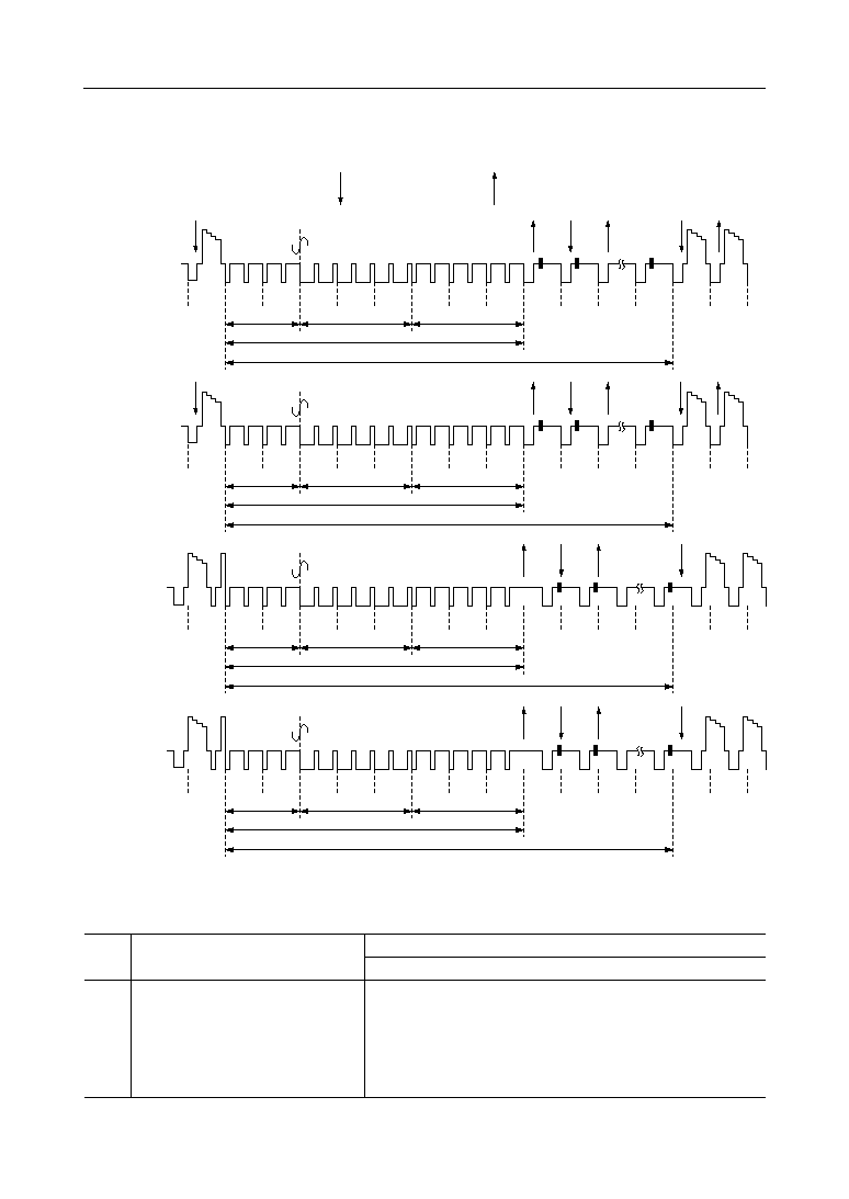
EAV(1st) EAV(2nd) EAV(3rd) EAV(4th)
DATA
CLKX1O
VALID DATA
OLR, OLG,
OLB, OLC
Input Timing
RELATIONSHIP BETWEEN BLANK SIGNAL AND INPUT IMAGE DATA
The blank signal is generated by the ITU Rec.656 standard input data. The input image data is
valid when the blank signal is "H".
° Semiconductor
MSM7653
14/35
VALID DATA RANGE
According to the ITU Rec.656 standard, the pixel data immediately from SAV (4th word) to a
fixed value before EVA is valid.
The following figure shows the relationship between the input data at the CCIR Rec.656 format
and the sync, luminance, chrominance signals which are processed inside the encoder.
Y00
8'h10
Luminance signal separated from
input data
Y01 Y10 Y11
8'h10
EAV
ITU Rec.656 standard input data
Note) The values in parenthesis indicate values in PAL mode.
Cb0, Y00, Cr0, Y01, Cb1, Y10, Cr1, Y11....
BLANK_L internally generated to
assure the horizontal and vertical
periods
Cb0
8'h80
Chrominance signal separated
from input data
Composite signal
Cr0 Cb1 Cr1
8'h80
711Tclkx1 (702Tclkx1)
20Tclkx1 (20Tclkx1)
127Tclkx1 (142Tclkx1)
1H
Sync signal BLANK_L generated
by input data
711Tclkx1 (702Tclkx1)
20Tclkx1 (20Tclkx1)
127Tclkx1 (142Tclkx1)
9Tclkx1 (16Tclkx1)
Sync signal HSYNC_L generated
by input data
63Tclkx1 (63Tclkx1) <Normal>
67Tclkx1 (67Tclkx1) <Colorstripe>
4Tclkx1
(4Tclkx1)
Sync signal VSYNC_L (1/2)
generated by input signal
1/2H
Sync signal VSYNC_L (0H)
generated by input signal
11Tclkx1 (4Tclkx1)
4Tclkx2
1716Tclkx2 (NTSC)/1728clkx2 (PAL)
1440T (NTSC/PAL)
136Tclkx1 (146Tclkx1)
SAV
4Tclkx2
EAV
Relationship between input data and sync signal, luminance signal, chrominance signals
° Semiconductor
MSM7653
15/35
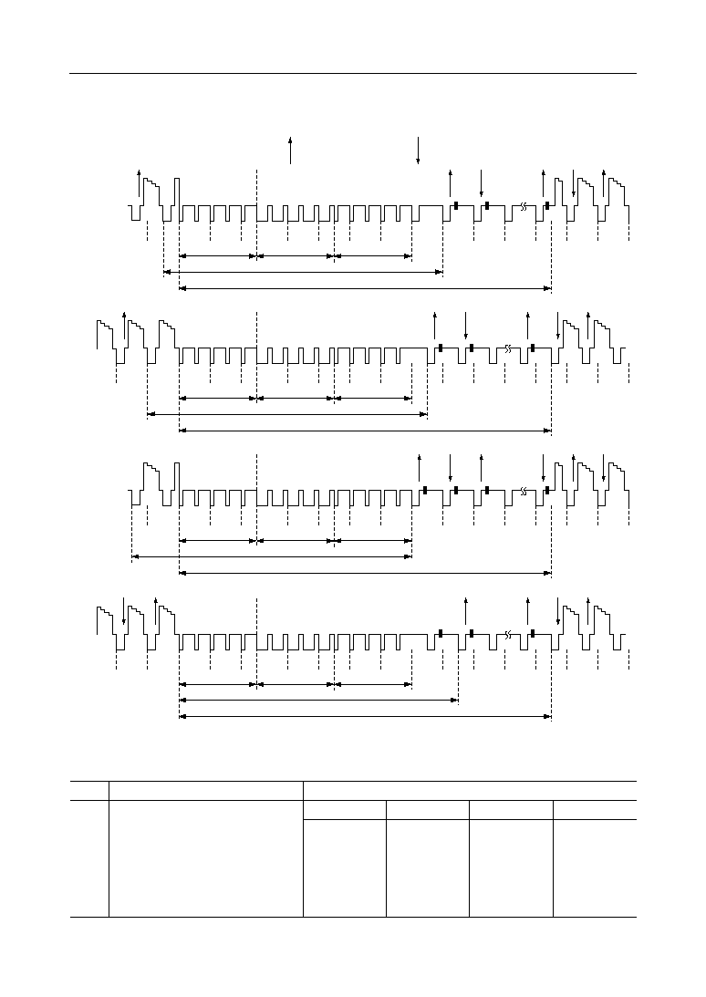
CLOCK TIMING2 (8bit Y/8bit CbCr input)
Input Data Timing
Input data and sync signals are fed into the encoder at the rising edge of CLKX2.
Input data is handled as valid pixel data when t
START
passes after the falling edge of HSYNC_L.
Chrominance signal of input data at this time is regarded as Cb.
don't care
don't care
YD, CD,
OLR, OLB,
OLG, OLC
HSYNC_L
CLKX2
BLANK_L
t
START
t
ACT
t
s1
t
h1
VALID DATA
ACTIVE VIDEO LINE
Video data input timing
Input data is recognized as valid pixel data when input signal BLANK_L is "H" in the t
ACT
period.
When BLANK_L is "H" during the blanking period, however, input data is not output as valid
pixel data since processing to maintain blanking period is internally in-progress.
The values of t
START
differ slightly between in master mode and in slave mode. The values of
t
START
are as follows.
In YCbCr format input mode, the values of t
START
are the same, in 8 bit (Y) + 8 bit (CbCr) mode
or in 8 bit (YCbCr) mode.
Operation mode
ITU 601 NTSC
ITU 601 PAL
In master mode
t
STA
(Ts)
250
280
Operation mode
ITU 601 NTSC
ITU 601 PAL
In slave mode
t
STA
(Ts)
260
290
t
STA
≠ t
S1
= t
START
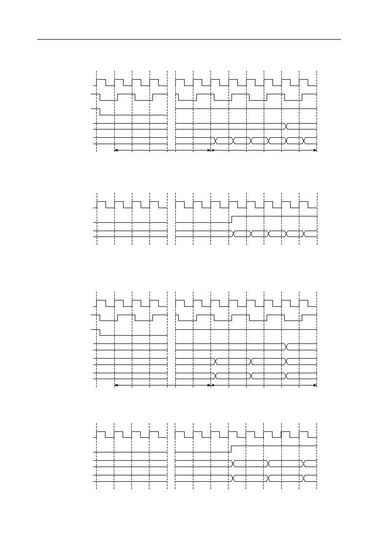
° Semiconductor
MSM7653
16/35
Timing of Input Data to HSYNC_L
Input Timing when BLANK_L is Input
Input timing at 27 MHz in YCbCr format
Timing of Input Data to HSYNC_L
Input Timing when BLANK_L is Input
Input timing at 13.5 MHz in YCbCr format
CLKX2
CLKX1O
HSYNC_L
OLR,OLG, OLB, OLC
YD
Invalid Data
Invalid Data
Invalid Data
Valid Data
Invalid Data
Cb0
Y00
Cr0
Y01
Cb1
Y10
t
START
t
ACT
CLKX2
BLANK_L
YD
Cb0
Y00
Cr0
Y01
Cb1
CLKX2
CLKX1O
HSYNC_L
OLR,OLG, OLB, OLC
CD
Invalid Data
Invalid Data
Invalid Data
Valid Data
Invalid Data
Cb0
Cr0
Cb1
YD
Invalid Data
Invalid Data
Y0
Y1
Y2
t
START
t
ACT
CLKX2
BLANK_L
YD
Y0
Y1
Y2
CD
Cb0
Cr0
Cb1
° Semiconductor
MSM7653
17/35
Internal Synchronization Output Timing
Output timing of HSYNC_L and VSYNC_L in master mode is as follows.
t
d1
t
d1
CLKX2
HSYNC_L
VSYNC_L
Output timing of internal synchronization, HSYNC_L and VSYNC_L
YA
VSYNC_L
523
524
525
1
2
3
4
5
6
7
17
18
Output timing of internal synchronization VSYNC_L
° Semiconductor
MSM7653
18/35
OUTPUT FORMAT
The timing conforms to the ITU624 standard.
In the NTSC operation mode, the existence/non-existence of setup level is selected by setting of
internal regsiters.
Data level on the DAC input terminal:
When the contents of 100% luminance order color bar are input into the encoder, the input level
is as follows.
≠20
0
7.5
11
20
30
41
59
70
89
100
133
≠40
114
224
266
285
338
390
450
549
610
715
775
957
4
DAC data Lumi (IRE)
Composite Wave Form (NTSC)
White
Yellow
Cyan
Green
Magenta
Red
Blue
Black
NTSC Composite Signal (Setup 7.5)

° Semiconductor
MSM7653
19/35
0
11
30
41
59
70
89
100
≠40
224
285
390
450
549
610
715
775
4
DAC data Lumi (IRE)
White
Yellow
Cyan
Green
Magenta
Red
Blue
Black
Y Wave Form (NTSC)
NTSC Y Signal Output (Setup 0)
≠20
0
≠59
≠63
20
44
59
63
≠44
402
512
188
166
622
754
836
858
270
DAC data Lumi (IRE)
Yellow
Cyan
Green
Magenta
Red
Blue
Color Burst
C Wave Form (NTSC)
NTSC C Signal Output
° Semiconductor
MSM7653
20/35
≠21.5
0
11
21.5
30
41
59
70
89
100
133
≠43
123
241
302
359
406
467
566
627
731
792
973
4
DAC data Lumi (IRE)
White
Yellow
Cyan
Green
Magenta
Red
Blue
Black
Composite Wave Form (PAL)
PAL Composite Signal
0
11
30
41
59
70
89
100
≠43
241
302
406
467
566
627
731
792
4
DAC data Lumi (IRE)
White
Yellow
Cyan
Green
Magenta
Red
Blue
Black
Y Wave Form (PAL)
PAL Y Signal Output
° Semiconductor
MSM7653
21/35
≠21.5
0
≠59
≠63
21.5
44
59
63
≠44
394
512
188
166
630
754
836
858
270
DAC data Lumi (IRE)
Yellow
Cyan
Green
Magenta
Red
Blue
Color Burst
C Wave Form (PAL)
PAL C Signal Output
° Semiconductor
MSM7653
22/35
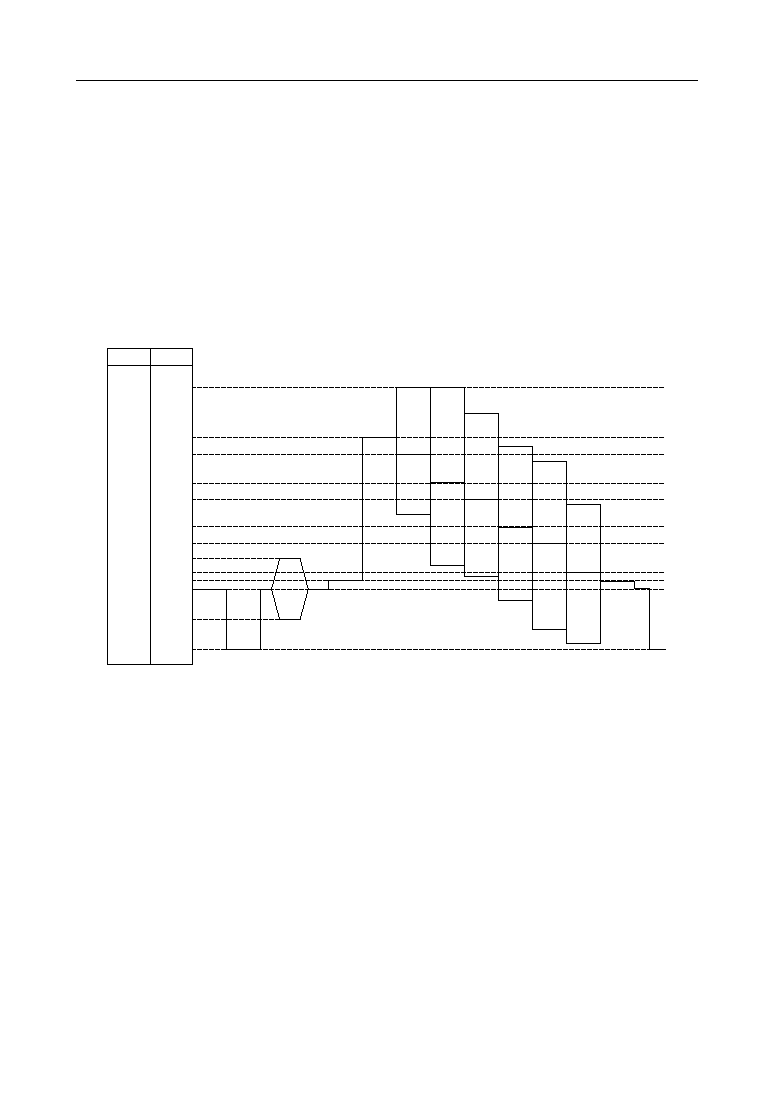
NTSC (Interlaced)
259
260
261
262 263
1
2
3
4
5
6
7
8
17
18
19
Field 1
Reference sub-carrier phase
NEGATIVE HALF CYCLE
Burst relative ≠180∞ to B-Y axis
POSITIVE HALF CYCLE
Burst relative 180∞ to B-Y axis
A
B
C
D
E
259
260
261
262 263
1
2
3
4
5
6
7
8
17
18
19
Field 2
Reference sub-carrier phase
A
B
C
D
E
259
260
261
262 263
1
2
3
4
5
6
7
8
17
18
19
Field 3
Reference sub-carrier phase
A
B
C
D
E
259
260
261
262 263
1
2
3
4
5
6
7
8
17
18
19
Field 4
Reference sub-carrier phase
A
B
C
D
E
Output timing (Interlaced NTSC)

° Semiconductor
MSM7653
23/35
Output timing (Interlaced NTSC)
Period
Odd field (Even field)
259.5 to 262.5H
1 to 3H
4 to 6H
1 to 6,259.5 to 262.5H
1 to 17,259.5 to 262.5H
Name
First equalizing pulse period (3H)
Vertical synchronization period (3H)
Second equalizing pulse period (3H)
Burst pause period
Vertical blanking period (20H)
Symbol
A
B
C
D
E
° Semiconductor
MSM7653
24/35
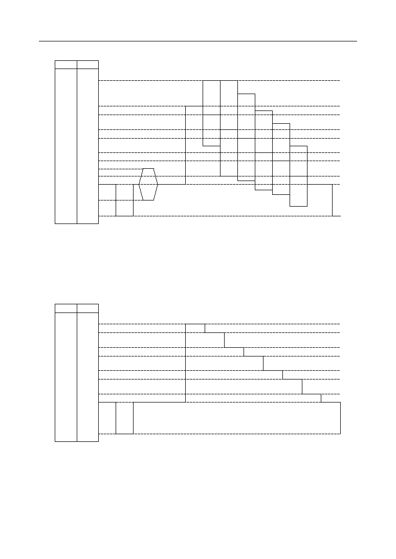
NTSC (Non-interlaced)
Output timing (Non-interlaced NTSC)
Period
Continuous odd ∑ even field
261 to 262H
1 to 3H
4 to 6H
261 to 6H
261 to 17H
Name
First equalizing pulse period (2H)
Vertical synchronization period (3H)
Second equalizing pulse period (2H)
Burst pause period
Vertical blanking period (19H)
Symbol
A
B
C
D
E
Output timing (Non-interlaced NTSC)
260
261
262
1
2
3
4
5
6
7
8
17
18
19
Continuous Odd Field
Reference sub-carrier phase
NEGATIVE HALF CYCLE
Burst relative ≠180∞ to B-Y axis
POSITIVE HALF CYCLE
Burst relative 180∞ to B-Y axis
A
B
C
D
E
260
261
262
1
2
3
4
5
6
7
8
17
18
19
Reference sub-carrier phase
A
B
C
D
E
260
261
262
1
2
3
4
5
6
7
8
17
18
19
Reference sub-carrier phase
A
B
C
D
E
Continuous Even Field
260
261
262
1
2
3
4
5
6
7
8
17
18
19
Reference sub-carrier phase
A
B
C
D
E
° Semiconductor
MSM7653
25/35
Output timing (Interlaced PAL)
Output timing (Interlaced PAL)
Period
Field 1,5
311 to 312.5H
1 to 2.5H
2.5 to 5H
1 to 6,310 to 312.5H
1 to 22.5,311 to 312.5H
Name
First equalizing pulse period (2.5H)
Vertical synchronization period (2.5H)
Second equalizing pulse period (2.5H)
Burst pause period
Vertical blanking period (25H)
Symbol
A
B
C
D
E
Field 3,7
311 to 312.5H
1 to 2.5H
2.5 to 5H
1 to 5,311 to 312.5H
1 to 22.5,311 to 312.5H
Field 2,6
311 to 312.5H
1 to 2.5H
2.5 to 5H
1 to 5.5,308.5 to 312.5H
1 to 22.5,311 to 312.5H
Field 4,8
311 to 312.5H
1 to 2.5H
2.5 to 5H
1 to 6.5,309.5 to 312.5H
1 to 22.5,311 to 312.5H
309
310
311
312 313
1
2
3
4
5
6
7
8
23
24
25
Field 1,5
Burst phase +135∞
+V
Burst phase -135∞
-V
A
B
C
D
E
Field 2,6
309
310
311
312 313
1
2
3
4
5
6
7
8
23
24
25
A
B
C
D
E
309
310
311
312 313
1
2
3
4
5
6
7
8
23
24
25
Field 3,7
A
B
C
D
E
Field 4,8
309
310
311
312 313
1
2
3
4
5
6
7
8
23
24
25
A
B
C
D
E
PAL (Interlaced)

° Semiconductor
MSM7653
26/35
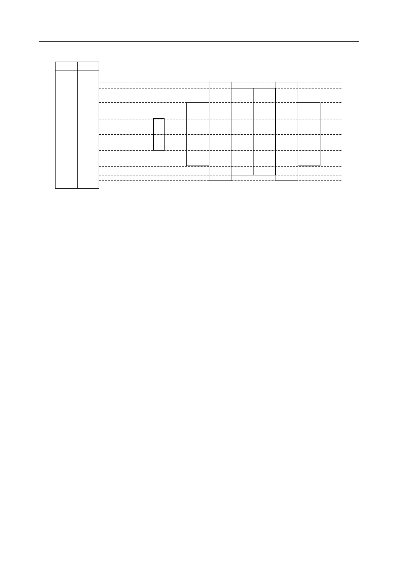
PAL (Non-interlaced)
310
311
312
1
2
3
4
5
6
7
8
23
24
25
Continuous Odd Field
Burst phase +135∞
+V
Burst phase -135∞
-V
A
B
C
D
E
309
310
311
312
1
2
3
4
5
6
7
8
23
24
25
A
B
C
D
E
309
310
311
312
1
2
3
4
5
6
7
8
23
24
25
Continuous Even Field
A
B
C
D
E
309
310
311
312
1
2
3
4
5
6
7
8
23
24
25
A
B
C
D
E
309
Output timing (Non-interlaced PAL)
Output timing (Non-interlaced PAL)
Period
Continuous odd ∑ even field
311 to 312H
1 to 2.5H
2.5 to 5H
311 to 6H
311 to 22H
Name
First equalizing pulse period (2H)
Vertical synchronization period (2.5H)
Second equalizing pulse period (2.5H)
Burst pause period
Vertical blanking period (24H)
Symbol
A
B
C
D
E
° Semiconductor
MSM7653
27/35
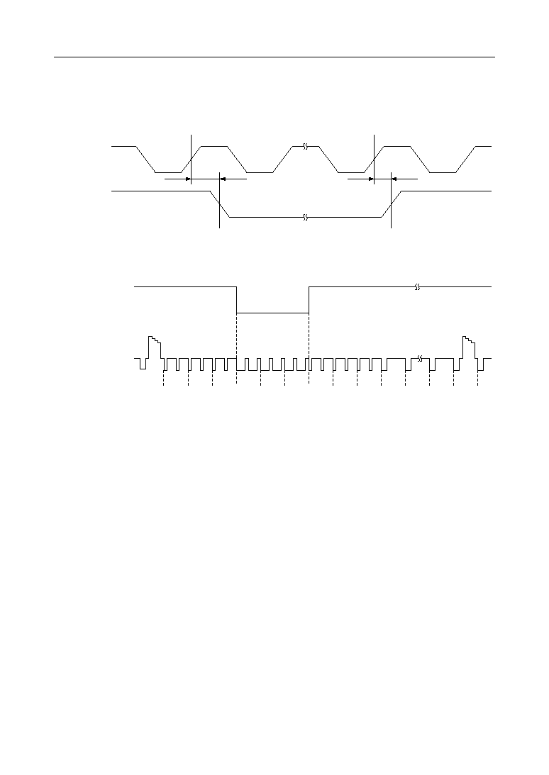
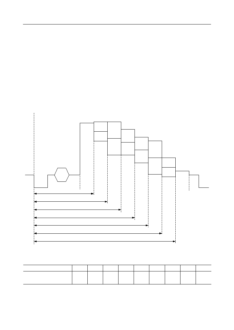
<Equalizing pulse, vertical synchronization period>
<Horizontal blanking period>
Horizontal blanking period
Setting content of equalizing pulse vertical
synchronization period (Ts is sampling clock cycle in each mode)
ITU 601 NTSC
ITU 601 PAL
q
31Ts
32Ts
w
365Ts
369Ts
e
64Ts
63Ts
1/2H
429Ts
432Ts
q
w
e
1/2H
1/2H
qEqualizing pulse width
wVertical sync pulse width
eSerration
qBlanking level
w
(synchronizing + blanking level) • (2/3)
e
(synchronizing + blanking level) • (1/3)
rSynchronzing level
r
e
w
q
EQUAL
q
w
e
r
t
1H
qHorizontal sync pulse width
wBurst signal output period
eBurst signal start
rHorizontal blanking period (excluding front porch)
tFront porch start
qSynchronzing level
w
(synchronizing + blanking level) • (1/3)
e
(synchronizing + blanking level) • (2/3)
rBlanking level
tPeak to peak value of burst
r
e
w
q
t
Setting content of horizontal blanking period (Ts is sampling clock cycle in each mode)
ITU601 NTSC
ITU601 PAL
q
63Ts
63Ts
w
31Ts
31Ts
e
71Ts
75Ts
r
127Ts
142Ts
t
838Ts
844Ts
Total dots/1H
858
864
Setting content of horizontal blanking period
° Semiconductor
MSM7653
28/35
Setup Level Setting
When the NTSC operation mode is selected, one of the two kinds of setup level can be selected
by setting of registers.
When the setup level 0 is selected, the Black-to-White is 100IRE.
When the setup level 7.5IRE is selected, the Black-to-White is 92.5IRE.
However, this setup function is valid only for the NTSC mode and invalid for the PAL mode.
Color Bar Generation Function
25%, 50%, 75% or 100% luminance order color bar is output by setting internal registers. The
output timings for each color bar color is as follows.
Contents of color bar output timing setting
ITU601 NTSC
ITU601 PAL
1H
858Ts
864Ts
u
750Ts
757Ts
y
661Ts
670Ts
t
572Ts
582Ts
r
483Ts
494Ts
e
394Ts
406Ts
w
305Ts
318Ts
q
216Ts
230Ts
hblank
127Ts
142Ts
Operation mode
(Ts : sampling block period)
White
q
w
e
r
t
y
u
Yellow
Cyan
Green
Magenta
Red
Blue
Black
Output timing of each color bar color
° Semiconductor
MSM7653
29/35
I
2
C BUS FORMAT
Basic input format of I
2
C-bus interface is shown below.
As described above, it is possible to read and write data from subaddress to subaddress
continuously. Reading from and writing to discontinuous addresses is performed by repeating
the Acknowledge and Stop condition formats after Data 0.
If one of the following matters occurs, the encoder will not return "A" (Acknowledge).
∑ The slave address does not match.
∑ A non-existent subaddress is specified.
∑ The read/write attribute of a register does not match "X" (read : 1/write : 0 control bit).
The input timing is shown below.
Slave Address
S
Subaddress
A
Data 0
A
A
.....
Data n
A
P
S
Slave Address
A
Subaddress
Data n
Description
Start condition
Slave address 1000100X (ADRS pin : 0) or 1000110X (ADRS pin : 1),
Acknowledge. Generated by slave
Subaddress byte
Data byte and acknowledge continues until data byte stop condition is met.
Symbol
P
Stop condition
the 8th bit is R (1)/W (0) signal.
1
2
7
8
9
ACK
1
2
3-8
9
ACK
S
Start Condition
P
Stop Condition
Change of Data Allowed
SCL
SDA
MSB
t
C_SCL
t
L_SCL
Data Line Stable: Data Valid
t
H_SCL
I
2
C-bus Basic Input/Output Timing
° Semiconductor
MSM7653
30/35
CLOSED CAPTION FUNCTION
The closed caption function based on the NCI standard is available.
The caption information on each line is multiplexed as a 26-cycle signal which is synchronized
at 503 kHz. Each cycle is described below.
Cycles 1 to 7
Clock-Run-in period
7-cycle clock signal to synchronize caption data
with caption information.
Cycles 8 to 10
Start Code
Fixed signal with logical level "001"
Cycles 11 to 26
Caption Information
2-byte multiplex information with combination of
the ASCII code bits 0 - 6 and the 7ODD parity bit.
The first byte is multiplexed in cycles 11 to 18 and
the second byte is multiplexed in cycles 19 to 26,
starting from LSB.
The output timing when data is multiplexed by the closed caption function is shown below.
1
Clock Run in
13.9 ms
(reference)
Cycle
50IRE
2
3
4
5
6
7
8
9 10 11 12 13 14 15 16 17 18 19 20 21 22 23 24 25 26
50IRE
20IRE
≠40IRE
0IRE
10.0 ms
(reference)
Start
Code
6.0 ms
(reference)
16-bit Information
Transition time
31.8 ms
(reference)
61.7 ms (reference)
Caption signal
Transition time
Transition time : ns
50%
100%
° Semiconductor
MSM7653
31/35
INTERNAL REGISTERS
The register (ID number) for the Anticopy function and the register (CCSTAT) for the closed
caption are read-only registers.
The other registers are write-only registers.
Details of the internal registers are described below. (Values marked * are set by default.)
Register name
R/W
Sub-
address
Default
value
Item to be set
Description
MR
(Mode register)
Write
Only
00
00
MR[4]
Override
Switching between the external terminal and
internal register settings (for the operation mode)
*0 : External pin setting enabled
1 : Internal register setting enabled
MR[3]
Chroma format
Chrominance signal input format
*0 : Offset binary
1 : 2's complement
MR[2]
Black level control
Black level setup
Note : Valid in NTSC mode only
*0 : Black level 0IRE
1 : Black level 7.5IRE
MR[0]
Video mode select
Operation mode switching
*0 : ITU601 NTSC
1 : ITU601 PAL
CR
(Command Register)
Write
Only
01
03
CR[4]
Undefined
--
CR[3]
Interlace
Scanning method
*0 : Interlace
1 : Non-interlace
CR[1:0]
Overlay level
Overlay signal/adjusting luminance order color
bar output level control
*00 : 100%
01 : 75%
10 : 50%
11 : 25%
MR[1]
Master/Slave
Master or slave operation select
*0 : Slave
1 : Master
CR[2]
Color bar
Adjusting luminance order color bar output control
*0 : Input image data or overlay data
1 : Luminance order color bar
(Note 1)
(Note 1) When the MR[4] register is set to "1" to enable the settings of the internal registers, the
settings of pin 7 (MODE) and the MR[0] register should be the same.
° Semiconductor
MSM7653
32/35
CCODT0
Write
Only
04
00
CCODT0[7:0]
1st byte of C.C. data, ODD field
First byte closed caption data in odd-number
field
CCODT1
Write
Only
05
00
CCODT1[7:0]
2nd byte of C.C. data, ODD field
Second byte closed caption data in odd-number
field
CCEDT0
Write
Only
06
00
CCEDT0[7:0]
1st byte of C.C. data, EVEN field
First byte closed caption data in even-number
field
CCEDT1
Write
Only
07
00
CCEDT1[7:0]
2nd byte of C.C. data, EVEN field
Second byte closed caption data in
even-number field
CCSTAT
Read
Only
08
00
CCSTAT[0]
Odd field C.C. status
odd-number field status
*0 : CCODT0, CCODT1 writing completed
1 : ODD Field C.C. bytes ENCODE completed
CCSTAT[1]
Odd field C.C. status
Even-number field status
*0 : CCEDT0, CCEDT1 writing completed
1 : EVEN Field C.C. bytes ENCODE completed
Register name
R/W
Sub-
address
Default
value
Item to be set
Description
CCEN
Write
Only
02
00
CCEN[1:0]
Closed Caption Enable
Closed caption function on/off control
*0 : C.C. encoding off
1 : Odd field encoding on
2 : Even field encoding on
3 : Both field encoding on
CCLN
Write
Only
03
11
CCLN[4:0]
Closed Caption Line Number
Closed caption data insertion line
number setting
NTSC : CCLN + 4
PAL : CCLN + 1
OPERATION MODE SETTING BY PIN CONTROL
The contents of control using TEST1, SEL1, SEL2, CLKSEL, and MS are shown below.
TEST1
0 : Normal operation
1 : Test mode
SEL1
0 : Normal operation
1 : Sleep mode
SEL2
0 : ITU Rec. 656
1 : Y Cb Cr
CLKSEL
0 : 27 MHz
1 : 13.5 MHz
MS
0 : Slave
1 : Master
TEST1
SEL1
SEL2
CLKSEL
MS
Operation mode
0
0
0
0
0
ITUR656 Slave
0
0
0
1
0
13.5 MHz YCbCr Slave
0
0
0
1
1
13.5 MHz YCbCr Master
0
0
1
0
0
27 MHz YCbCr Slave
0
0
1
0
1
27 MHz YcbCr Master
0
1
x
x
x
Sleep Mode
x : don't care

° Semiconductor
MSM7653
33/35
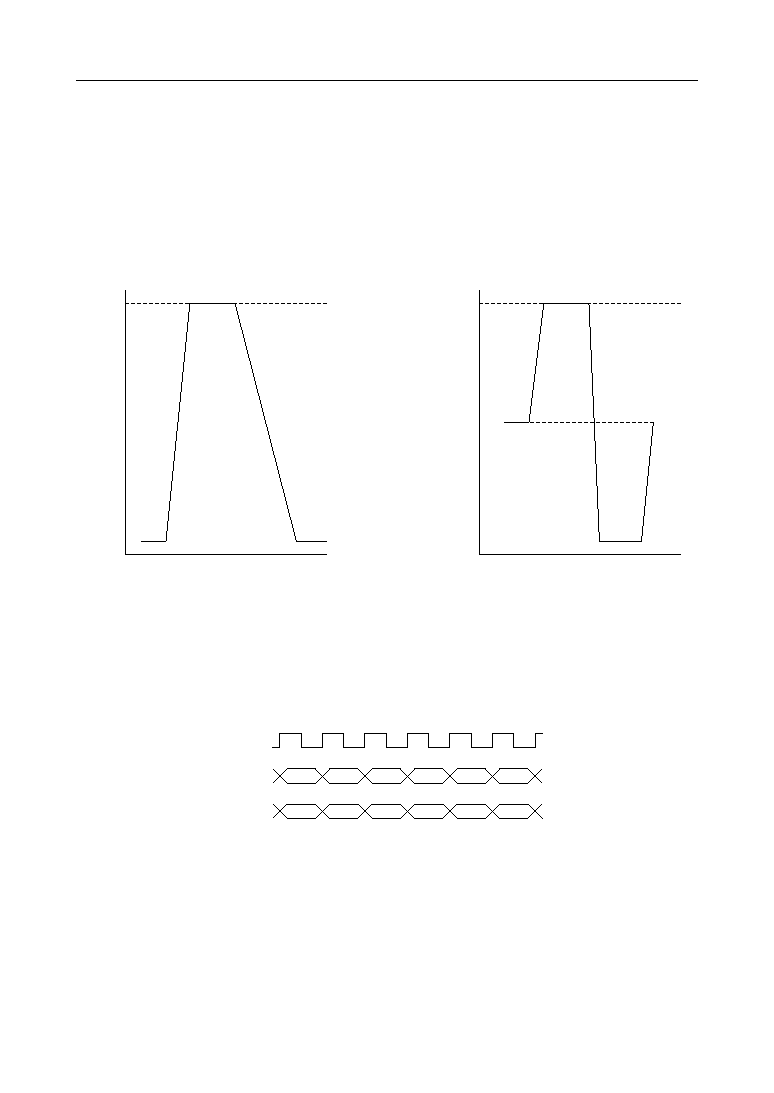
FILTER CHARACTERISTICS
The characteristics of LPF used for color signal processing and interpolation filters used for
upsampling processing are shown below.
LPF for 422 color signals
The following shows the characteristics when the clock frequency is 13.5 MHz.
≠100
≠80
≠60
≠40
≠20
0
0
1
2
3
4
5
6
7
422 Interpolation + LPF Frequency Characteristic
Frequency [MHz]
Level [dB]
≠100
≠80
≠60
≠40
≠20
0
0
2
4
6
8
10
12
14
Up Sampling Filter Frequency Characteristic
Frequency [MHz]
Level [dB]
Interpolation
The following shows the characteristics when the clock frequency is 27 MHz.
(Note) The characteristics of these filters are based on design data.
° Semiconductor
MSM7653
34/35
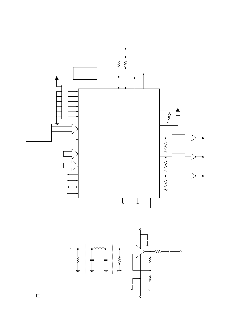
APPLICATION CIRCUIT EXAMPLE
Recommended Analog Output Circuit
150 W
3.6 mH
164 pF
OUTPUT
YA
CA
CVBSO
150 W
164 pF
0.1 mF
0.1 mF
75 W
560 W
560 W
≠AVCC
+AVCC
1000 mF
+
+
≠
LPF (Toko-make 621LJN-1471 is recommended.)
CLKSEL
SEL1
DIP SW
OLR
OLG
OLB
OLC
Overlay
Controller
BLANK_L
HSYNC_L
VSYNC_L
CLKX1O
CD[7:0]
CD[7:0]
YD[7:0]
YD[7:0]
MSM7653
CLKX2
V
REF
FS
COMP
YA
LPF
AMP
R1
CVBSO
LPF
AMP
R1
CA
LPF
AMP
R1
C
C
= 0.1
µ
F
Typ. 1.25 V
R
C
SCL
SDA
I
2
C
Controller
R
L
R
L
5 V or 3.3 V
DV
DD
3.3 V
AV
DD
3.3 V
5 V or 3.3 V
3.3 V
DGND
AGND
OUTSEL
MODE
MS
SEL2
R
C
= 500
VR
Note: The termination of a DA converter analog output with a 37.5 W load eliminates need for
an AMP.

° Semiconductor
MSM7653
35/35
PACKAGE DIMENSIONS
(Unit : mm)
56-Pin Plastic QFP

NOTICE
1.
The information contained herein can change without notice owing to product and/or
technical improvements. Before using the product, please make sure that the information
being referred to is up-to-date.
2.
The outline of action and examples for application circuits described herein have been
chosen as an explanation for the standard action and performance of the product. When
planning to use the product, please ensure that the external conditions are reflected in the
actual circuit, assembly, and program designs.
3.
When designing your product, please use our product below the specified maximum
ratings and within the specified operating ranges including, but not limited to, operating
voltage, power dissipation, and operating temperature.
4.
Oki assumes no responsibility or liability whatsoever for any failure or unusual or
unexpected operation resulting from misuse, neglect, improper installation, repair, alteration
or accident, improper handling, or unusual physical or electrical stress including, but not
limited to, exposure to parameters beyond the specified maximum ratings or operation
outside the specified operating range.
5.
Neither indemnity against nor license of a third party's industrial and intellectual property
right, etc. is granted by us in connection with the use of the product and/or the information
and drawings contained herein. No responsibility is assumed by us for any infringement
of a third party's right which may result from the use thereof.
6.
The products listed in this document are intended for use in general electronics equipment
for commercial applications (e.g., office automation, communication equipment,
measurement equipment, consumer electronics, etc.). These products are not authorized
for use in any system or application that requires special or enhanced quality and reliability
characteristics nor in any system or application where the failure of such system or
application may result in the loss or damage of property, or death or injury to humans.
Such applications include, but are not limited to, traffic and automotive equipment, safety
devices, aerospace equipment, nuclear power control, medical equipment, and life-support
systems.
7.
Certain products in this document may need government approval before they can be
exported to particular countries. The purchaser assumes the responsibility of determining
the legality of export of these products and will take appropriate and necessary steps at their
own expense for these.
8.
No part of the contents contained herein may be reprinted or reproduced without our prior
permission.
Copyright 1999 Oki Electric Industry Co., Ltd.
Printed in Japan
E2Y0002-29-62