 | –≠–ª–µ–∫—Ç—Ä–æ–Ω–Ω—ã–π –∫–æ–º–ø–æ–Ω–µ–Ω—Ç: MSM7662 | –°–∫–∞—á–∞—Ç—å:  PDF PDF  ZIP ZIP |

° Semiconductor
MSM7662
1/62
PEDL7662-02
° Semiconductor
MSM7662
NTSC/PAL Digital Video Decoder
GENERAL DESCRIPTION
The MSM7662 is an LSI device that decodes NTSC or PAL analog video signals into YCbCr and
RGB digital data based on ITU-RBT.601.
The device has built-in two channels of A/D converters and can accept composite video and S
video signals for the input video signals. Composite video signals are converted to YCbCr and
RGB digital data via the 2-dimensional Y/C separation circuit with an adaptive filter.
Analog video signals can be sampled by a clock at the pixel frequency or at twice the pixel
frequency. A decimation filter is built-in for sampling at twice the pixel frequency.
Input signals are synchronized internally and high-speed locking for color burst is possible.
Because a FIFO buffer is built into the output format circuit, jitter-free output can be obtained
even for non-standard signals.
APPLICATION EXAMPLES
Since the synchronization of input signals and high-speed locking for color burst are possible, the
device is optimized for applications used by switching multiple cameras.
It is also used for various image processing applications because of jitter-free output data
through a built-in FIFO buffer.
8-bit (YCbCr), 16-bit (8-bit (Y) + 8-bit (CbCr)), and 24-bit (RGB) output interfaces can be selected
as an output mode so that various devices such as monitoring system, digital video memory,
digital TV, video processing unit and video communication unit can be selected on the receiving
side.
FEATURES (∑ new feature not found on MSM7661B)
∑ Input analog signal
NTSC/PAL composite video signal or S-video signal
∑ Maximum 5 composite or 2 S-video + 2 composite analog inputs can be connected (switchable
by external pins or internal registers)
∑ Built-in clamp circuits and video amps
∑ Built-in 8-bit A/D converters (2 channels)
∑ 4 selectable output interfaces
ITU-RBT.656 (conditional)
8-bit (YCbCr)
: 8-bit (YCbCr) YCbCr = 4 : 2 : 2/YCbCr = 4 : 1 : 1 (limit)
16-bit (YCbCr)
: 8-bit (Y) + 8-bit (CbCr) YCbCr = 4 : 2 : 2/YCbCr = 4 : 1 : 1 (limit)
24-bit RGB
: 8-bit (R) + 8-bit (G) + 8-bit (B)
∞
2-dimensional Y/C separation using adaptive comb filter (this filter is bypassed for S-video
signal input)
NTSC format: 3 lines or 2 lines, PAL format: 2 lines (3 virtual lines)
∑ Selectable data I/O signal synchronization
4 synchronization modes, internal FIFO modes (FIFO-1, FIFO-2) and external field memory
modes (FM-1, FM-2), are selectable (FIFO-1 is normally selected).
PEDL7662-02
This version: Oct. 1999
Previous version : Oct. 1998
Preliminary

° Semiconductor
MSM7662
2/62
PEDL7662-02
∞
Compatible pixel frequencies (normal/twice the pixel frequency)
13.5 MHz (13.5/27 MHz)
: NTSC/PAL ITU-RBT.601
12.272727 MHz (12.272727/24.545454 MHz)
: NTSC Square pixel
14.31818 MHz (14.31818/28.63636 MHz)
: NTSC 4fsc
14.75 MHz (14.75/29.5 MHz)
: PAL Square Pixel
∑ Built-in AGC/ACC circuits, compatible with a wide range of input levels
Input level range: ≠8 dB to +3.5 dB (0.4 V to 1.5 V)
Switchable between AGC/MGC (fixed gain) and ACC/MCC (fixed gain)
∞
Decimation filter built into input stage, allows easy configuration of filter prior to A/D
converter (when input at twice the pixel frequency)
∞
Automatic NTSC/PAL recognition (only for ITU-RBT.601)
∞
Sleep mode
∞
Multiplex signal recognition (closed caption)
During vertical blanking interval, data is output as 8-bit data.
∞
I
2
C-bus interface
∞
3.3 V single power supply (I/O 5 V tolerance)
∞
Package:
100-pin plastic TQFP (TQFP100-P-1414-0.50-K) (Product name: MSM7662TB)
° Semiconductor
MSM7662
3/62
PEDL7662-02
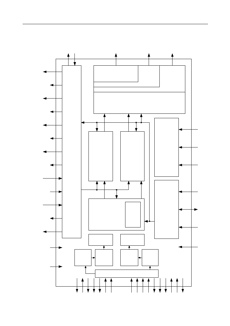
BLOCK DIAGRAM
SCAN
Test Control Logic
SLEEP
TEST[2:0]
STATUS2
STATUS3
ODD/EVEN
STATUS1
HVALID
VVALID
HSYNC_L
VSYNC_L
Synchronization Block
Luminance Block
DIGITAL
(AGC or MGC + LPF)
CLKSEL
GAINS[2:0]
INS[2:0]
PLLSEL
CLKXO
CLKX2
CLKX2O
VRCL1
VRT1
VIN2
VIN3
VIN4
CLPOUT2
VRB2
VIN6
VIN5
AMPOUT2
ADIN2
VRT2
ADIN1
AMPOUT1
CLPOUT1
VRB1
VIN1
M[7:4]
M[2:1]
Y[7:0]
(G[7:0])
Epilogue
Block
Output
Formatter
8 bits (R)
8 bits (G)
8 bits (B)
8 bits (Y)
8 bits (CbCr)
ITU-656
&
8 bits
(YCbCr)
C[7:0]
(R[7:0])
B[7:0]
Prologue Block
C ADC
Decimation
Filter
Line Memory
(1 KB)
• 2
(2 Dim. Y/C separate)
Chrominance Block
(ACC or MCC + LPF)
SDA
I
2
C-bus Control Logic
SCL
MODE[3:0]
RESET_L
Y ADC
Decimation
Filter
ANALOG
AGC&
AMP
ANALOG
AGC&
AMP
SW Matrix
° Semiconductor
MSM7662
4/62
PEDL7662-02
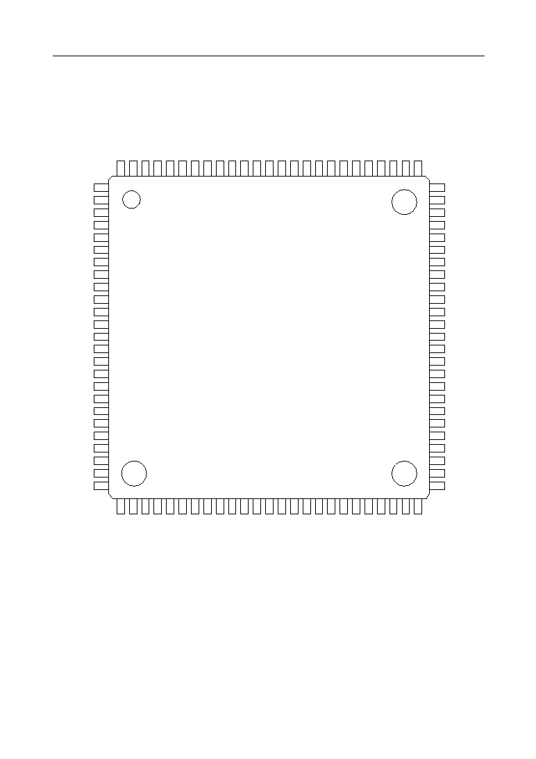
PIN CONFIGURATION (TOP VIEW)
100
99
98
97
96
95
94
93
92
91
90
DAGND
INS[0]
INS[1]
INS[2]
GAINS[0]
GAINS[1]
GAINS[2]
DV
DD
M[0]
M[1]
DGND
75
74
73
72
71
70
69
68
67
66
65
HSYNC_L
VSYNC_L
VVALID
HVALID
ODD/EVEN
C[0]
C[1]
C[2]
C[3]
C[4]
C[5]
1
2
3
4
5
6
7
8
9
10
11
DAV
DD
VRT2
VIN6
VIN5
AD
DD
AGND
ADIN2
AMPOUT2
CLPOUT2
VRB2
AGND
89
M[2]
88
M[3]
87
M[4]
86
M[5]
85
M[6]
12
AGND
13
VRB1
14
CLPOUT1
15
AMPOUT1
16
ADIN1
64 C[6]
63 C[7]
62 DGND
61 DV
DD
60 Y[0]
84
M[7]
83
STATUS1
82
STATUS2
81
STATUS3
26
27
28
29
30
31
32
33
34
35
36
DAGND
MODE[0]
MODE[1]
MODE[2]
MODE[3]
SCAN
TEST[2]
TEST[1]
TEST[0]
SLEEP
RESET_L
37
DV
DD
38
DGND
39
SCL
40
SDA
41
PLLSEL
42
CLKSEL
43
B[7]
44
B[6]
45
B[5]
17
VRCL1
18
AGND
19
AV
DD
20
VIN4
59 Y[1]
58 Y[2]
57 Y[3]
56 Y[4]
80
CLKX2
79
DV
DD
78
DGND
77
CLKX2O
76
CLKXO
46
B[4]
47
B[3]
48
B[2]
49
B[1]
50
B[0]
21
VIN3
55 Y[5]
22
VIN2
23
VIN1
24
VRT1
25
DAV
DD
54 Y[6]
53 Y[7]
52 DV
DD
51 DGND
,
100-Pin Plastic TQFP
° Semiconductor
MSM7662
5/62
PEDL7662-02
PIN DESCRIPTIONS
Pin
Symbol
Type
Description
1
DAV
DD
--
Digital power supply in A/D converter
2
VRT2
O
A/D converter reference voltage (high side) for S-video chroma signal
3
VIN6
I
S-video 2 chroma signal (C-2) input pin
(leave open or connect to AGND when not used)
4
VIN5
I
Composite-5 or S-video 1 chroma signal (C-1) input pin
(leave open or connect to AGND when not used)
5
AV
DD
--
Analog power supply
6
AGND
--
Analog ground
7
ADIN2
I
A/D converter input pin for S-video chroma signal
8
AMPOUT2
O
S-video chroma signal amp output
9
CLPOUT2
O
S-video chroma signal clamp voltage output
10
VRB2
O
A/D converter reference voltage (low side) for S-video chroma signal
11
AGND
--
Analog ground
12
AGND
--
Analog ground
13
VRB1
I
A/D converter reference voltage (low side) for composite/S-video
(luminance signal)
14
CLPOUT1
O
Composite/S-video (luminance signal) clamp voltage output
15
AMPOUT1
O
Composite/S-video (luminance signal) amp output
16
ADIN1
I
A/D converter input pin for composite/S-video (luminance signal)
17
VRCL1
I
S-video (luminance signal) clamp voltage input
18
AGND
--
Analog ground
19
AV
DD
--
Analog power supply
20
VIN4
I
Composite-4 input (leave open or connect to AGND when not used)
21
VIN3
I
Composite-3 input (leave open or connect to AGND when not used)
22
VIN2
I
Composite-2 S-video 2 luminance signal (Y-2) input
(leave open or connect to AGND when not used)
23
VIN1
I
Composite-1 S-video 1 luminance signal (Y-1) input
(leave open or connect to AGND when not used)
24
VRT1
O
A/D converter reference voltage (high side) for composite/S-video
(luminance signal)
25
DAV
DD
--
Digital power supply in A/D converter
26
DAGND
--
Digital ground in A/D converter
° Semiconductor
MSM7662
6/62
PEDL7662-02
PIN DESCRIPTIONS (continued)
Pin
Symbol
Type
Description
31
SCAN
I
Not used. Be left open or fixed at "0" (pulled down by internal resistor).
32
TEST[2]
I
Not used. Be left open or fixed at "0" (pulled down by internal resistor).
33
TEST[1]
I
Not used. Be left open or fixed at "0" (pulled down by internal resistor).
34
TEST[0]
I
Not used. Be left open or fixed at "0" (pulled down by internal resistor).
35
SLEEP
I
0: normal operation, 1: sleep operation
36
RESET_L
I
Reset input pin (active "L"). After powering ON, be sure to reset.
37
DV
DD
--
Digital power supply
38
DGND
--
Digital ground
39
SCL
I
I
2
C-bus clock input
40
SDA
I/O
I
2
C-bus data I/O pin
41
PLLSEL
I
Not used. Be left open or fixed at "0" (pulled down by internal resistor).
42
CLKSEL
I
Clock select input pin (pulled down by internal resistor).
0: double-speed input mode 1: normal input mode
When a double-speed input mode is used, input a double frequency to system clock.
43 to 50
B[7] to B[0]
O
Data output B[7]: MSB, B[0]: LSB
During RGB output mode: B 8-bit data output
Other than RGB output mode: Hi-Z
Output mode is set by pin 27 or 28, or register MRA [7:6].
51
DGND
--
Digital ground
52
DV
DD
--
Digital power supply
27
MODE[0]
I
I/O switching input during external setting mode
(pulled-down by internal resistors)
28
29
30
MODE[1]
MODE[2]
MODE[3]
Internal/external pins are switched by register MRA[0]
The default of register MRA[0] is external pin mode.
MODE [3:2]
MODE [1] Input mode selection
Invalid if an ITU-RBT.601 signal is input while the register MRC[7] is set
to automatic NTSC/PAL recognition.
MODE [0] Input mode selection
NTSC 4fsc can be set by register MRA [3:1] only.
Output mode selection
00: ITU-RBT.656 (with 8-bit YCbCr SAV, EAV, blank processing)
01: 8-bit (YCbCr)
10: 16-bit (YCbCr) (ITU-RBT.601)
11: 24-bit RGB
0: NTSC 1: PAL
0: ITU-RBT.601 1: Square Pixel
I
I
I

° Semiconductor
MSM7662
7/62
PEDL7662-02
PIN DESCRIPTIONS (continued)
Pin
Symbol
Type
Description
53 to 60
Y[7] to Y[0]
O
Data output Y[7]: MSB, Y[0]: LSB
During ITU-RBT.656 output mode: YCbCr 8-bit data output
During 8-bit (YCbCr) output mode: YCbCr 8-bit data output
During 16-bit (YCbCr) output mode: Y 8-bit data output
During 24-bit RGB output mode: G 8-bit data output
Output mode is set by pin 27 or 28, or register MRA [7:6].
61
DV
DD
--
Digital power supply
62
DGND
--
Digital ground
63 to 70
C[7] to C[0]
O
Data output C[7]: MSB, C[0]: LSB
During ITU-RBT.656 output mode: Hi-Z
During 8-bit (YCbCr) output mode: Hi-Z
During 16-bit (YCbCr) output mode: CbCr 8-bit data output
During 24-bit RGB output mode: R 8-bit data output
Output mode is set by pin 27 or 28, or register MRA [7:6].
71
ODD/EVEN
O
Field display output
If field is odd, "H" is output.
72
HVALID
O
Horizontal valid pixel timing output pin
If section is valid, "H" is output.
73
VVALID
O
Vertical valid line timing output pin
If section is valid, "H" is output.
74
VSYNC_L
O
Vertical sync signal (V sync) output pin
75
HSYNC_L
O
Horizontal sync signal (H sync) output pin
76
CLKXO
O
Pixel clock output
During double-speed input mode (pin 42 = 0): One half of system clock
frequency is output.
During normal input mode (pin 42 = 1): The same frequency as system
clock frequency is output.
77
CLKX2O
O
System clock output
System clock input is directly output.
78
DGND
--
Digital ground
79
DV
DD
--
Digital power supply
80
CLKX2
I
System clock input (selected by operation mode)
NTSC ITU-RBT.601
NTSC Square Pixel
NTSC 4fsc
PAL ITU-RBT.601
PAL Square Pixel
Normal input mode
13.5 MHz
12.272727 MHz
14.31818 MHz
13.5 MHz
14.75 MHz
Double-speed input mode
27 MHz
24.545454 MHz
28.63636 MHz
27 MHz
29.5 MHz
° Semiconductor
MSM7662
8/62
PEDL7662-02
PIN DESCRIPTIONS (continued)
Pin
Symbol
Type
Description
82
STATUS[2]
O
Status signal output
Selected by internal register OMR[1]
OMR[1]: 0
OMR[1]: 1
83
STATUS[1]
O
VBI interval multiplex signal detection output
0: non-detection, 1: detection
84
M[7]
O
Field memory control signal; RE output
85
M[6]
O
Field memory control signal; WE output
86
M[5]
O
Field memory control signal; RSTR output
87
M[4]
O
Field memory control signal; RSTW output
88
M[3]
O
Test output pin, normally "L" output
89
M[2]
I
I
2
C-bus slave address select
0: 1000001X
1: 1000011X (no internal pull-up or pull-down resistor)
90
M[1]
I
Pin for setting by either external pin or internal register in order to select
analog unit gain value (MGC) and video signal input pin.
(no internal pull-up or pull-down resistor)
0: external pin mode
Gain value setting: pins 94 to 96 (GAINS[2:0]) are used
Input pin setting: pins 97 to 99 (INS[2:0]) are used
1: register mode
Gain value setting: register ADC2[6:4]
Input pin setting: register ADC1[2:0]
Internal register setting is invalid when external pin mode is set.
91
M[0]
I
Selection of external field memory control signal output
If field memory is not used, set M[0] to 0.
0: M[7:4] outputs are invalid
1: M[7:4] outputs are valid
92
DGND
--
Digital ground
93
DV
DD
--
Digital power supply
NTSC-PAL recognition (default)
0: NTSC, 1: PAL
HLOCK sync detection output
0: non-detection, 1: detection
81
STATUS[3]
O
Status signal output
Selected by internal register OMR[0]
OMR[0]: 0
OMR[0]: 1
FIFO overflow detection (default)
0: non-detection, 1: detection
CSYNC output
° Semiconductor
MSM7662
9/62
PEDL7662-02
Pin
Symbol
Type
Description
94
GAINS[2]
I
Inputs for amplifier gain switch setting during external setting mode
97
INS[2]
I
Inputs for signal input pin switch setting during external setting mode
100
DAGND
--
Digital ground in A/D converter
95
GAINS[1]
96
GAINS[0]
External pin mode: pin 90 (M[1]) = 0
(pulled down by internal resistors)
GAINS[2:0]
[000]
[001]
[010]
[011]
[100]
[101]
[110]
[111]
Gain value (x times)
1.00
1.35
1.75
2.30
3.00
3.80
5.00
Undefined
98
INS[1]
99
INS[0]
External pin mode: pin 90 (M[1]) = 0
(pulled down by internal resistors)
INS[2:0]
[000]
[001]
[010]
[011]
[100]
[101]
[110]
[111]
Input pin
VIN1 (pin 23) Composite-1
VIN2 (pin 22) Composite-2
VIN3 (pin 21) Composite-3
VIN4 (pin 20) Composite-4
VIN5 (pin 4) Composite-5
VIN1 (pin 23) Y-1
VIN5 (pin 4) C-1
VIN2 (pin 22) Y-2
VIN6 (pin 3) C-2
Prohibited setting (ADC enters sleep state)
I
I
I
I
PIN DESCRIPTIONS (continued)
° Semiconductor
MSM7662
10/62
PEDL7662-02
ABSOLUTE MAXIMUM RATINGS
Parameter
Power Supply Voltage
Input Voltage
Power Consumption
Storage Temperature
Symbol
V
DD
V
I
P
W
T
STG
Condition
Ta = 25∞C
V
DD
= 3.3 V
--
--
Rating
≠0.3 to +4.5
≠0.3 to +5.5
1
≠55 to +150
Unit
V
V
W
∞C
RECOMMENDED OPERATING CONDITIONS
Parameter
Power Supply Voltage
Power Supply Voltage
Digital "H" Level Input Voltage
Digital "L" Level Input Voltage
Symbol
V
DD
GND
V
IH1
V
IL
Condition
--
--
--
--
Typ.
3.3
0
--
--
Unit
V
V
V
V
Operating Temperature
Ta
--
--
∞C
Min.
3.0
--
2.2
0
0
Max.
3.6
--
V
DD
(*2)
V
IH2
(*1)
--
--
V
0.8
• V
DD
V
DD
(*2)
0.8
70
Analog Video Signal Input
V
AIN
SYNC tip to white
peak level
--
V
P-P
0.8
1.1
*1:
CLKSEL, SDA, CLKXO
*2:
Since the inputs have a tolerance of up to 5.5 V, it is possible to apply 5 V to the inputs.

° Semiconductor
MSM7662
11/62
PEDL7662-02
ELECTRICAL CHARACTERISTICS
DC Characteristics
Parameter
Symbol
V
OH
Condition
I
OH
= ≠6 mA (*2)
I
OL
= 6 mA (*2)
Typ.
--
Unit
"L" Level Output Voltage
V
OL
--
V
Min.
0.7
• V
DD
0
Max.
V
DD
0.4
"H" Level Output Voltage
V
Input Leakage Current
I
I
V
I
= GND to V
DD
--
mA
mA
≠10
+10
Output Leakage Current
I
O
V
I
= GND to V
DD
--
mA
≠10
+10
SDA Output Voltage
SDAV
L
--
--
V
0
0.4
SDA Output Current
SDAI
O
--
--
mA
3
--
I
OH
= ≠4 mA (*1)
I
OL
= 4 mA (*1)
R
pull_down
=
--
20
250
50 k
W (*3)
(Ta = 0 to 70∞C, V
DD
(DV
DD
, ADV
DD
, AV
DD
) = 3.3 V ±0.3 V)
*1:
HSYNC_L, VSYNC_L, SYSSEL, C[7:0], B[7:0], ODD, VVALID, HVALID, CLKXO, HSY,
M[7:0]
*2:
Y[7:0], CLKX2O
*3:
MODE[3:0], SCAN, TEST[2:0], PLLSEL, CLKSEL, GAINS[2:0], INS[2:0]
DC Characteristics (Analog Unit)
Parameter
Symbol
Condition
Typ.
Unit
Min.
Max.
AMPOUT Output Voltage
V
OAMP
R
O
= 300
W
--
V
0.3
2.4
CLPOUT Output Voltage
V
OCLP
R
O
= 5 k
W
--
V
0.2
1.6
VRT Output Voltage
V
RT
(*)
2.3
V
2.0
2.4
VRB Output Voltage
V
RB
(*)
0.3
V
0.15
0.4
ADIN
V
IADIN
--
--
V
V
RB
V
RT
VIN
V
IVIN
Capacitive coupling
--
V
P-P
0.4
1.3
Input Current
I
IVIN
V
I
= 1.5 V
--
mA
5
30
(Ta = 0 to 70∞C, V
DD
(DV
DD
, ADV
DD
, AV
DD
) = 3.3 V ±0.3 V, GND = 0 V)
*:
10 kW connected between V
RT
and V
RB
DC Characteristics
Parameter
Symbol
Condition
Typ.
Unit
Min.
Max.
Power Supply Current (Operating)
I
D1
AD1 on
AD2 off
CLKX2 = 27 MHz
150
mA
120
210
Power Supply Current (Operating)
I
D2
AD1 on
AD2 on
CLKX2 = 27 MHz
170
mA
140
240
Power Supply Current (Sleep)
I
DOFF
V
I
= 1.5 V
mA
0
5
(Ta = 0 to 70∞C, V
DD
(DV
DD
, ADV
DD
, AV
DD
) = 3.3 V ±0.3 V, GND = 0 V)
° Semiconductor
MSM7662
12/62
PEDL7662-02
AC Characteristics (Double Speed Mode)
Parameter
Symbol
Condition
Min.
Typ.
Max.
Unit
CLKX2 Cycle Frequency
1/t
CLKX2
ITU-RS601
--
27.0
--
MHz
NTSC 4fsc
--
28.63636
--
MHz
NTSC Square Pixel
--
24.545454
--
MHz
PAL Square Pixel
--
29.5
--
MHz
Output Data Delay Time 1 (*)
t
OD21
CLKSEL : L
7 (5)
--
26 (24)
ns
Output Data Delay Time 2 (*)
t
OD22
CLKSEL : L
6 (4)
--
22 (20)
ns
t
CXD21
CLKSEL : L
5
--
20
ns
Output Clock Delay Time (*)
(CLKX2-CLKX2O)
t
CXD22
CLKSEL : L
4
--
17
ns
(*) Output load: 40 pF
Values in the parentheses indicate the delay time when 8-bit YCbCr format data is output from the Y pin.
The clock frequency accuracy is within ±100 ppm.
SCL Clock Cycle Time
t
C_SCL
R
pull_up
= 4.7 k
W
200
--
--
ns
SCL Low Level Cycle
t
L_SCL
R
pull_up
= 4.7 k
W
100
--
--
ns
Output Clock Delay Time (*)
(CLKX2-CLKXO)
(Ta = 0 to 70∞C, V
DD
(DV
DD
, ADV
DD
, AV
DD
) = 3.3 V ±0.3 V, GND = 0 V)
CLKX2 Duty
t
D_D2
--
45
--
55
%
Output Data Delay Time 3 (*)
t
OD23
CLKSEL : L
7 (5)
--
30 (28)
ns
Output Data Delay Time 1X1 (*)
t
ODX21
CLKSEL : L
2
--
8
ns
Output Data Delay Time 1X2 (*)
t
ODX22
CLKSEL : L
1
--
5
ns
Output Data Delay Time 1X3 (*)
t
ODX23
CLKSEL : L
2
--
10
ns
Output Data Delay Time 2X1 (*)
t
OD2X21
CLKSEL : L
3 (1)
--
11 (9)
ns
Output Data Delay Time 2X2 (*)
t
OD2X22
CLKSEL : L
2 (1)
--
9 (7)
ns
Output Data Delay Time 2X3 (*)
t
OD2X23
CLKSEL : L
3 (1)
--
13 (11)
ns
RESET_L Width
t
RST_W
200
--
--
ns

° Semiconductor
MSM7662
13/62
PEDL7662-02
AC Characteristics (Single Speed Mode)
Parameter
Symbol
Condition
Min.
Typ.
Max.
Unit
CLKX2 Cycle Frequency
1/t
CLKX2
ITU-RS601
--
13.5
--
MHz
NTSC 4fsc
--
14.31818
--
MHz
NTSC Square Pixel
--
12.272727
--
MHz
PAL Square Pixel
--
14.75
--
MHz
Output Data Delay Time 1 (*)
t
OD11
CLKSEL : H
8
--
26
ns
Output Data Delay Time 2 (*)
t
OD12
CLKSEL : H
7
--
22
ns
t
CXD11
CLKSEL : H
6
--
20
ns
Output Clock Delay Time (*)
(CLKX2-CLKX2O)
t
CXD12
CLKSEL : H
5
--
17
ns
(*) Output load: 40 pF
The clock frequency accuracy is within ±100 ppm.
SCL Clock Cycle Time
t
C_SCL
R
pull_up
= 4.7 k
W
200
--
--
ns
SCL Low Level Cycle
t
L_SCL
R
pull_up
= 4.7 k
W
100
--
--
ns
Output Clock Delay Time (*)
(CLKX2-CLKXO)
(Ta = 0 to 70∞C, V
DD
(DV
DD
, ADV
DD
, AV
DD
) = 3.3 V ±0.3 V, GND = 0 V)
CLKX2 Duty
t
D_D1
CLKSEL : H
40
60
%
Output Data Delay Time 3 (*)
t
OD13
CLKSEL : H
8
--
30
ns
Output Data Delay Time 1X1 (*)
t
ODX11
CLKSEL : H
2
--
8
ns
Output Data Delay Time 1X2 (*)
t
ODX12
CLKSEL : H
1
--
5
ns
Output Data Delay Time 1X3 (*)
t
ODX13
CLKSEL : H
2
--
12
ns
Output Data Delay Time 2X1 (*)
t
OD2X11
CLKSEL : H
3
--
11
ns
Output Data Delay Time 2X2 (*)
t
OD2X12
CLKSEL : H
2
--
8
ns
Output Data Delay Time 2X3 (*)
t
OD2X13
CLKSEL : H
3
--
15
ns
RESET_L Width
t
RST_W
200
--
--
ns
° Semiconductor
MSM7662
14/62
PEDL7662-02
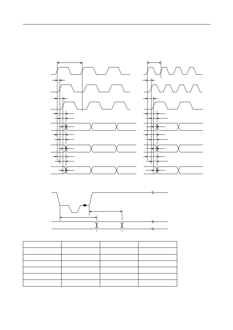
INPUT AND OUTPUT TIMING
Clock and Output Timing
Data Delay (when a standard signal is input)
The data delay is equal to the blank delay. 1H depends on the sampling mode.
The numeric value (T value) may be changed according to a signal state.
Since the output period is fixed during FIFO mode, the amount of delay is changed.
If Y/C separation is performed using TRAP filter during PAL mode, 1H is not added.
T = 1 pixel rate,
a = absorption difference
Video Mode
Input Signal
FIFO/FM Mode
Amount of Delay
NTSC
Composite
FIFO-1
1H + 358T ±
a
NTSC
Composite
FM
1H + 358T
PAL
Composite
FIFO-1
1H + 358T ±
a
PAL
Composite
FM
1H + 358T
NTSC, PAL
S-Video
FIFO-1
358T ±
a
NTSC, PAL
S-Video
FM
358T
CLKX2O
CLKX2
CLKXO
t
CXD21
t
CXD11
t
CXD22
t
CXD21
t
CLKX1
CLKSEL: L
Y[7:0], C[7:0]
B[7:0]
t
CLKX2
t
OD11
t
OD21
t
OD12
t
OD22
t
OD2X11
t
OD2X21
t
ODX11
t
ODX21
t
OD2X12
t
OD2X22
t
ODX12
t
ODX22
t
OD13
t
OD23
t
OD2X13
t
OD2X23
t
ODX13
t
ODX23
HVALID, VVALID,
ODD
HSYNC_L,
VSYNC_L
STATUS[3:1]
M[7:4]
CLKSEL: H
Data delay
Analog Video In
Decoder output
Blank
Blank delay
Active Data
° Semiconductor
MSM7662
15/62
PEDL7662-02
I
2
C-bus Interface Input/Output Timing
The basic input/output timing of the I
2
C-bus is indicated below.
1
2
7
8
9
ACK
1
2
3-8
9
ACK
S
Start condition
P
Stop condition
Data line stable: data valid
Change of data allowed
SCL
SDA
MSB
t
C_SCL
I
2
C-bus Timing
The I
2
C-bus timing conforms to this table. However, the I
2
C-bus can operate faster than at the
speeds, specified above. Actually, the SCL frequency is up to about 5 MHz. The hold time and
setup time in that case must conform to the ratio described in the above table.
Symbol
Parameter
Min.
Unit
f
SCL
SCL Frequency
0
kHz
t
BUF
Bus Open Period
4.7
ms
t
HD: STA
Start Condition Hold Time
4.0
ms
t
LOW
Clock Low Period
4.7
ms
t
HIGH
Clock High Period
4.0
ms
t
SU: STA
Start Condition Setup Time
4.7
ms
t
HD: DAT
Data Hold Time
300
ns
t
SU: DAT
Data Setup Time
250
ns
t
R
Line Rise Time
ms
t
F
Line Fall Time
ns
t
SU: STO
Stop Condition Setup Time
4.7
ms
100
1
300
Max.
S
P
SCL
SDA
t
BFU
t
HD:STA
S
P
t
LOW
t
HD:DAT
t
R
t
F
t
HD:STA
t
HIGH
t
SU:DAT
t
SU:STA
t
SU:STO
° Semiconductor
MSM7662
16/62
PEDL7662-02
FUNCTIONAL DESCRIPTION
Analog Unit
1) Analog input select: Compatible with composite video signals and S-video signals. Input
selection can be switched by register control via the I
2
C-bus or by
external pins. (See the below chart for pin combinations.)
2) Clamp function:
An analog clamp and a digital pulse clamp can be used.
Analog clamp
Analog clamp ∆ Digital clamp (hybrid clamp)
Digital clamp
Only the digital clamp can be set as the pedestal clamp.
# Related register MRB[3:2]
3) AGC amp:
The AGC function operates depending upon the input level.
Manual gain setting is also possible. This AGC function operates at 2
stages, the analog unit and digital unit. Digital decoded data is output
in conformance with ITU-RBT.601.
Refer to the explanation of M[1] pin (pin 90).
# Related register ADC2[6:4]
4) A/D converter:
Two internal 8-bit A/D converters sample at twice the pixel frequency.
(Sampling at the pixel frequency is possible by changing the register
setting.)
# Related register ADC1[2:0]
List of Analog Input Conditions
Input Signal
Control Pin
Input Pin
ADC Selection
INS[2:0]
VIN1
VIN2
VIN3
VIN4
VIN5
VIN6
ON
OFF
Composite-1 Input*
[000]
Composite
ON
OFF
Composite-2 Input
[001]
Composite
ON
OFF
Composite-3 Input
[010]
Composite
ON
OFF
Composite-4 Input
[011]
Composite
ON
OFF
Composite-5 Input
[100]
Composite
ON
OFF
S-video-1 Input
[101]
Luminance
Chroma
ON
ON
S-video-2 Input
[110]
Luminance
Chroma
ON
ON
All inputs Off
[111]
OFF (Sleep)
OFF
OFF
Register
ADC1[2:0]
[000]
[001]
[010]
[011]
[100]
[101]
[110]
[111]
Blank spaces: non-selectable
*: register default setting after LSI reset
M[1] pin setting
0: external mode, 1 internal register mode
° Semiconductor
MSM7662
17/62
PEDL7662-02
Manual Gain Control (analog AMP gain)
Gain Setting Pins
GAINS[2:0]
Set Gain Value
Typ. Value (multiplication factor)
[000]
1.0
[001]
1.35
[010]
1.75
[011]
2.3
[100]
3.0
[101]
3.8
[110]
5.0
[111]
Undefined
Register
ADC2[6:4]
[000]
[001]
[010]
[011]
[100]
[101]
[110]
[111]

° Semiconductor
MSM7662
18/62
PEDL7662-02
Decoder Unit
1. Prologue Block
The prologue block inputs data and performs Y/C separation.
Data can be input at either the pixel frequency (ITU-RBT.601: 13.5 MHz) or at twice the pixel
frequency (ITU-RBT.601: 27 MHz). If input at twice the pixel frequency, data is processed after
passing through a decimator circuit to convert it to the pixel frequency. The decimator circuit
may be bypassed by changing the register setting, regardless of whether data is input at the
normal pixel frequency or at twice the pixel frequency.
If a composite signal (CVBS) is input, the default setting performs Y/C separation using a 2-
dimensional adaptive comb filter.
The following operating modes can be selected via the I
2
C-bus. Default settings are indicated by
an asterisk (*). The default state is selected at reset.
1) Video input mode selection (related register MRC[7])
NTSC/PAL auto-select* (only for ITU-RBT.601)
Dependent upon operating mode selected
When ITU-RBT.601 is selected, the video input mode is automatically set depending upon
the number of lines per field.
2) Operating mode selection (related register MRA[3:1])
NTSC ITU-RBT.601
13.5 MHz*
NTSC Square Pixel
12.272727 MHz
NTSC 4fsc
14.31818 MHz
PAL ITU-RBT.601
13.5 MHz
PAL Square Pixel
14.75 MHz
Even if input at twice the pixel frequency, the internal processing is performed at the pixel
frequency.
3) Decimator circuit pass/bypass selection (related register MRC[4])
Pass through decimator circuit*
Bypass decimator circuit
Compatible only when input at twice the pixel frequency.
4) Y/C separation mode selection (related register MRB[1:0])
Use adaptive comb filter*
Use non-adaptive comb filter
Do not use comb filter (use trap filter)
The adaptive comb filter for a NTSC signal makes the correlation between up to 3 consecutive
lines, and Y/C separation is performed by the 3-line or 2-line comb filter according to the format
of correlation.
The adaptive comb filter for a PAL signal makes the correlation between only 2 lines and
performs Y/C separation by switching between the 2-line comb filter and trap filter.
The non-adaptive comb filter performs Y/C separation by removing the luminance component
based on the average of preceding and following lines (when there is correlation between 3 lines).
(the average of 2 lines in the case of a PAL signal)
When a comb filter is not used, Y/C separation is performed by a trap filter.

° Semiconductor
MSM7662
19/62
PEDL7662-02
If an S-video signal is input, these Y/C separation circuits are bypassed.
The functions of this block only operate when lines are valid as image information. During the
V blanking interval, CVBS signals are not processed.
2. Luminance Block
The luminance block removes synchronous signals from signals containing luminance components
after Y/C separation. The signals are compensated and then output as luminance signals. Two
modes of gain control functions can be selected for the luminance signal output level: AGC (Auto
Gain Control) and MGC + Pedestal Clamp.
In the AGC mode, luminance level amplification is determined by comparing the SYNC depth
with a reference value. The default is 40IRE and can be changed by the register setting. The input
has a sync tip clamp.
In the MGC + Pedestal Clamp mode, the signal output level is clamped to the pedestal level of
the input. Signal amplification and black level can be changed from the clamped position by
register settings.
This block can select the follwing operating modes.
1) Selection of luminance level limiter usage (related register LUMC[7])
Do not use*
Use
When a limiter is used, the luminance level is limited to 16 to 235.
2) Selection of prefilter and sharp filter usage (related register LUMC[6])
Do not use*
Use
These filters are used to enhance the edges of luminance component signals.
Two filters operate in pairs. For their characteristics, refer to Filter Characteristics described
later.
3) Selection of aperture bandpass filter coefficient (related register LUMC[5:4])
Middle range*
High range
4) Coring range selection (related register LUMC[3:2])
Off*
±
4LBS
±
5LBS
±
7LBS
5) Aperture weighting coefficient selection (related register LUMC[1:0])
0*
0.25
0.75
1.50
Both coring and aperture compensation processes perform contour compensation.
6) Selection of pixel position compensating circuit usage (related register MRC[6])
Use*
Do not use

° Semiconductor
MSM7662
20/62
PEDL7662-02
7) AGC loop filter time constant selection (related register AGCLF[7:6])
Slow
convergence time
903 ms
Medium
225 ms*
Fast
56 ms
Fixed
0
These are designed times from the input gain being rapidly lowered to 50% (≠6 dB) of the
value at a stable state when normal signals are input till the output being returned to ≠1 dB
(actually these times differ depending on the signal state).
Fixed: manual gain setting is possible by register AGCLF[5:0]
8) Parameter for fine adjustment of AGC sync depth (related register AGCLF[5:0])
AGC reference level is changed.
9) Parameter for fine adjustment of sync removal level (related register SSEPL[6:0])
The black level is adjusted. The default setting outputs the pedestal position as a black level
(=16).
10)Pedestal clamp selection (related register SSEPL[7])
Do not use pedestal clamp*
Use pedestal clamp (at this time, AGC does not operate, MGC operates)
3. Chrominance Block
This block processes the chroma signals.
The following operating modes can be selected.
1) Selection of chroma bandpass filter usage (related register CHRC[2])
Do not use*
Use
2) ACC loop filter time constant selection (related register ACCLF[6:5])
Slow
convergence time
1696 ms
Medium
424 ms*
Fast
106 ms
Fixed
0
These are designed times from the input gain being rapidly lowered to 50% (≠6 dB) of the
value at a stable state when normal signals are input till the output being returned to ≠1 dB
(actually these times differ depending on the signal state).
Fixed: manual gain setting is possible by register ACCLF[4:0]
3) ACC reference level fine adjustment (related register ACCLF[4:0])
ACC reference level is changed.
4) Parameter for burst level fine adjustment (related register CHRC[1:0])
Threshold level at which chroma amplitude becomes valid is selected based upon color burst
ratio.
0.5
0.25*
0.125
Off
Off: The color killer function is turned off. If decoloration occurs while decoding a still picture,
setting the threshold level to "off" will reduce the decoloration.
5) Color killer mode selection (related register MRB[5])
Auto color killer mode*
Forced color killer
6) Parameter for fine adjustment of color subcarrier phase (related register HUE[7:0])
HUE control function

° Semiconductor
MSM7662
21/62
PEDL7662-02
In this block, chroma signals pass through a bandpass filter to cut out unnecessary band.
To maintain a constant chroma level, these signals then pass through an ACC compensating
circuit and are UV demodulated. (The filter can be bypassed.)
If the demodulated result does not reach a constant level, color killer signals are generated to fix
the ACC gain. This functions as an auto color killer control circuit.
The UV demodulated results pass through a low-pass filter and are output as chrominance
signals.
4. Synchronization Block
This block processes the sync signals. Synchronous signals are generated for chip output and for
internal use. Various signals are output from this block and the following operating modes can
be selected.
1) Adjustment of SYNC threshold level (internal sync) (related register STHR[7:0])
SYNC detection level is set.
2) Fine adjustment of HSY (Horizontal Sync Clamp) signal (related registers HSYT[7:4], HSYT[3:0],
MRB[3:2])
2-1) Fine adjustment of HSY signal (start side)
2-2) Fine adjustment of HSY signal (stop side)
The HSY signal provides the sync-tip and clamp timing to the A/D converter.
This signal is used for digital clamp, but can not be observed from outside.
3) Fine adjustment of HSYNC_L signal (related register HSDL[7:0])
HSYNC_L signal output position is adjusted.
4) HVALID control (related registers HVALT[7:4], HVALT[3:0])
4-1) Fine adjustment of HVALID signal (start side)
4-2) Fine adjustment of HVALID signal (stop side)
Data signals are transferred at the rising edge of the HVALID signal.
5) VVALID control (related registers VVALT[7:4], VVALT[3:0])
5-1) Fine adjustment of VVALID signal (start side)
5-2) Fine adjustment of VVALID signal (stop side)
6) FIFO and Field Memory mode selection (related register MRB[7:6])
FIFO-1 mode*: Sets and outputs a standard value for the number of pixels per 1H from the
internal FIFO.
This mode is also compatible (to a degree) with non-standard VTR signals.
FIFO-2 mode: Sets and outputs a constant pixel number corresponding to the input H
interval for the number of pixels per 1H from the internal FIFO.
FM-1 mode:
This mode outputs the decoded results according to the SYNC signal.
Usage of external field memory is required to manage the number of pixels
and to absorb jitter.
Memory control signals are to be generated externally.
FM-2 mode:
This mode is compatible with considerably distorted non-standard VTR
signals. Jitter is absorbed by using external field memory (2 Mb • 2) and the
standard value is set as the pixel number.
Field memory control signals are output simultaneously from M[7:4].
7) Field memory control signals
If the FM-2 mode uses external field memory (2 Mb • 2) instead of the internal FIFO, field
memory control signals are supplied from pins M[7:4]. At this time, pin M[0] requires to be
set to "H".

° Semiconductor
MSM7662
22/62
PEDL7662-02
5. Epilogue Block
The Epilogue Block outputs the UV signal from the Chrominance block and the Y signal from the
Luminance block in a format based on a signal obtained from the control register setting.
This block can select the following modes.
1) Output mode selection (related register MRA[7:6])
1-1) ITU-RBT.656 (SAV, EAV, blank processing)
1-2) * 8-bit (YCbCr) output (2x pixel clock)
synchronization with HSYNC_L, VSYNC_L
1-3) 16-bit (8-bit Y/8-bit CbCr) (pixel clock)
synchronization with HSYNC_L, VSYNC_L
1-4) 24-bit RGB (8 bits each)
synchronization with HSYNC_L, VSYNC_L
2) Enable Blue Back display when synchronization fails (related register MRB[4])
OFF
ON*
If "H" is not input when no signal is output or when synchronization fails, a vertical
synchronizing signal (VSYNC_L) is not output.
3) Selection of YCbCr signal output format (related register MRC[5])
YCbCr
4 : 2 : 2*
YCbCr
4 : 1 : 1
The chrominance signal (U, V component) outputs Cb and Cr data to the C pin in an output
format to be described later.
4) Output pin enable selection (related register OMR[2])
High-impedance
Output enable*
This setting is valid during sleep mode only.
All the data output pins and sync signal output pins become high impedance.
5) Multiplex signal (VBI data) detection level adjustment (related register OMR[5:3])
The levels to detect multiplexed signals sent during the vertical blanking period are
configured to be variable. The binary values after input signals are A-to-D converted are
employed as the levels to detect multiplexed signals, and the levels are set in eight steps on
the basis of a value obtained from reducing the SYNC tip level to 0.
6) Various mode detection (related register OMR[1:0])
NTSC/PAL detection
Multiplex signal detection
HSYNC synchronization detection
Internal FIFO overflow detection
7) Output signal phase control (related registers OPCY[1:0], OPCC[1:0])
Y and C phases can each be adjusted in the range of ≠2 to +1 pixels.
6. I
2
C Control Block
This serial interface block is based on the I
2
C standard of the Phillips Corporation.
The registers at up to subaddress Hex14 are write-only registers and the register at subaddress
Hex20 is a read-only register.
The license to use the LSI chip for I
2
C systems is granted on the basis of the I
2
C patent of the
Phillips Corporation by purchasing the LSI chip.
7. Test Control Block
This block is used to test the LSI chip. Normally this block is not used.

° Semiconductor
MSM7662
23/62
PEDL7662-02
Input Signal Level
The figure below shows the recommended range of the input signal, received in an 8-bit straight
binary format.
reserved
255
Iuminance
200
sync
NTSC:60
(PAL:63)
4
0
chrominance
+DC
input black level
13
246
input sync-tip level
CVBS[7:0] input range
The above input conditions are ideal. Because analog signals are normally input at different
levels, the exact settings described above are difficult to achieve. While maintaining the ratio of
White Peak (100%)/SYNC = 100IRE/40IRE (NTSC), if the input signal is set within the A/D
converter's voltage range/the Y digital output will be output by digital AGC operation with the
pedestal position set at the black level (16) and the white peak position (100%) set at the peak level
(235) even if the peak level does not reach 196 (200 ≠ 4).
° Semiconductor
MSM7662
24/62
PEDL7662-02
Output format
ITU-RBT.656 output, 8-bit (YCbCr) output, and 16-bit (8-bit Y/8-bit CbCr) output have the
following formats.
The YCbCr 4:2:2 format and 4:1:1 format are shown below.
The output format can be changed by register settings.
Pixel Byte Sequence
Output
Y7 (MSB)
Y6
Y5
Y4
Y3
Y2
Y1
Y0 (LSB)
Y7
Y6
Y5
Y4
Y3
Y2
Y1
Y0
Y7
Y6
Y5
Y4
Y3
Y2
Y1
Y0
Y7
Y6
Y5
Y4
Y3
Y2
Y1
Y0
Y7
Y6
Y5
Y4
Y3
Y2
Y1
Y0
Y7
Y6
Y5
Y4
Y3
Y2
Y1
Y0
Y7
Y6
Y5
Y4
Y3
Y2
Y1
Y0
C7 (MSB)
C6
C5
C4
C3
C2
C1
C0 (LSB)
Cb7
Cb6
Cb5
Cb4
Cb3
Cb2
Cb1
Cb0
Cb7
Cb6
Cb5
Cb4
Cb3
Cb2
Cb1
Cb0
Cr7
Cr6
Cr5
Cr4
Cr3
Cr2
Cr1
Cr0
Cb7
Cb6
Cb5
Cb4
Cb3
Cb2
Cb1
Cb0
Cr7
Cr6
Cr5
Cr4
Cr3
Cr2
Cr1
Cr0
Cr7
Cr6
Cr5
Cr4
Cr3
Cr2
Cr1
Cr0
Y point
0
2
YCbCr 4:2:2 format
3
4
5
1
C point
0
2
4
Pixel Byte Sequence
Output
Y7 (MSB)
Y6
Y5
Y4
Y3
Y2
Y1
Y0 (LSB)
Y7
Y6
Y5
Y4
Y3
Y2
Y1
Y0
Y7
Y6
Y5
Y4
Y3
Y2
Y1
Y0
Y7
Y6
Y5
Y4
Y3
Y2
Y1
Y0
Y7
Y6
Y5
Y4
Y3
Y2
Y1
Y0
Y7
Y6
Y5
Y4
Y3
Y2
Y1
Y0
Y7
Y6
Y5
Y4
Y3
Y2
Y1
Y0
C7 (MSB)
C6
C5
C4
C3
C2
C1
C0 (LSB)
Cb7
Cb6
Cr7
Cr6
0
0
0
0
Cb5
Cb4
Cr5
Cr4
0
0
0
0
Y point
0
2
3
4
5
1
C point
0
4
YCbCr 4:1:1 format
Y7
Y6
Y5
Y4
Y3
Y2
Y1
Y0
Y7
Y6
Y5
Y4
Y3
Y2
Y1
Y0
6
7
Cb7
Cb6
Cr7
Cr6
0
0
0
0
Cb5
Cb4
Cr5
Cr4
0
0
0
0
Cb3
Cb2
Cr3
Cr2
0
0
0
0
Cb1
Cb0
Cr1
Cr0
0
0
0
0
Cb3
Cb2
Cr3
Cr2
0
0
0
0
Cb1
Cb0
Cr1
Cr0
0
0
0
0
° Semiconductor
MSM7662
25/62
PEDL7662-02
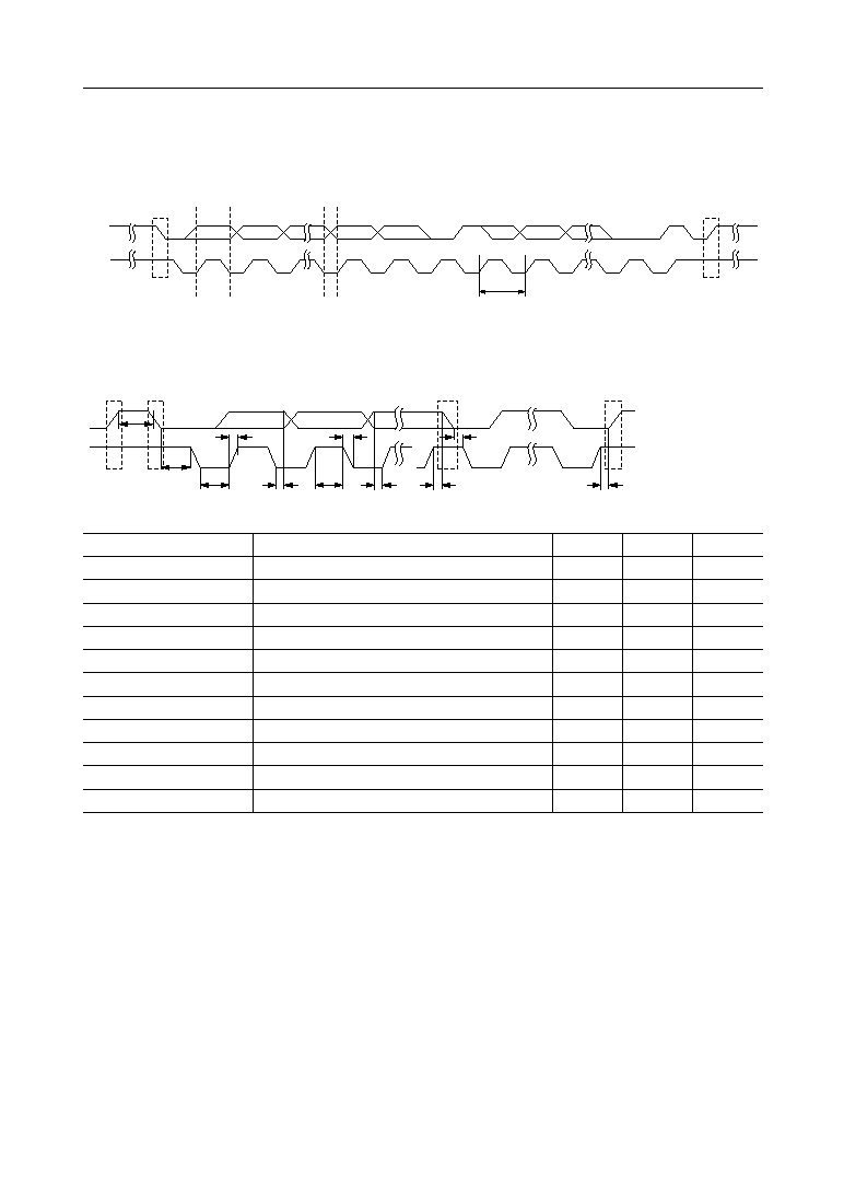
TIMING DESCRIPTION
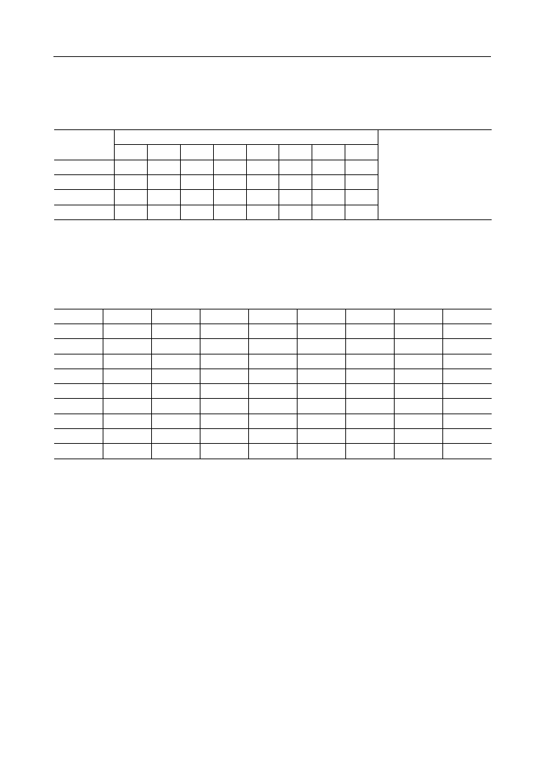
Vertical Synchronizing Signal
The vertical synchronizing signal timing is as follows. The default output is as shown below, but
the internal processing of the synchronizing signal is performed before 1H.
524
525
1
2
3
4
5
6
7
8
9
21
22
CVBS
HVALID
HSYNC_L
VSYNC_L
VVALID
ODD
262
263
264
265
266
267
268
269
270
271
283
284
285
CVBS
HVALID
HSYNC_L
VSYNC_L
VVALID
ODD
CSYNC_L
CSYNC_L
Vertical Synchronizing Signal (60 Hz)
° Semiconductor
MSM7662
26/62
PEDL7662-02
621
622
623
624
625
1
2
3
4
5
6
23
24
CVBS
HVALID
HSYNC_L
VSYNC_L
VVALID
ODD
309
310
311
312
313
314
315
316
317
318
336
337
338
CVBS
HVALID
HSYNC_L
VSYNC_L
VVALID
ODD
CSYNC_L
CSYNC_L
Vertical Synchronizing Signal (50 Hz)
° Semiconductor
MSM7662
27/62
PEDL7662-02
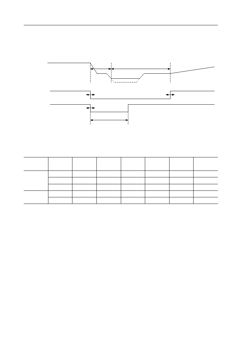
A/D Converter Support Signal
The waveform of the HSY signal, shown below, provides clamp timing to the A/D converter
when HSY clamp (digital clamp) is selected. The start and end edges of the clamp pulse have a
variable range from the sync tip to the pedestal position. (HSY is an internal signal.)
COLOR
BURST
CVBS
BURST
HSY
Pedestal
sync tip
A/D Converter Support Signal
Output Timing
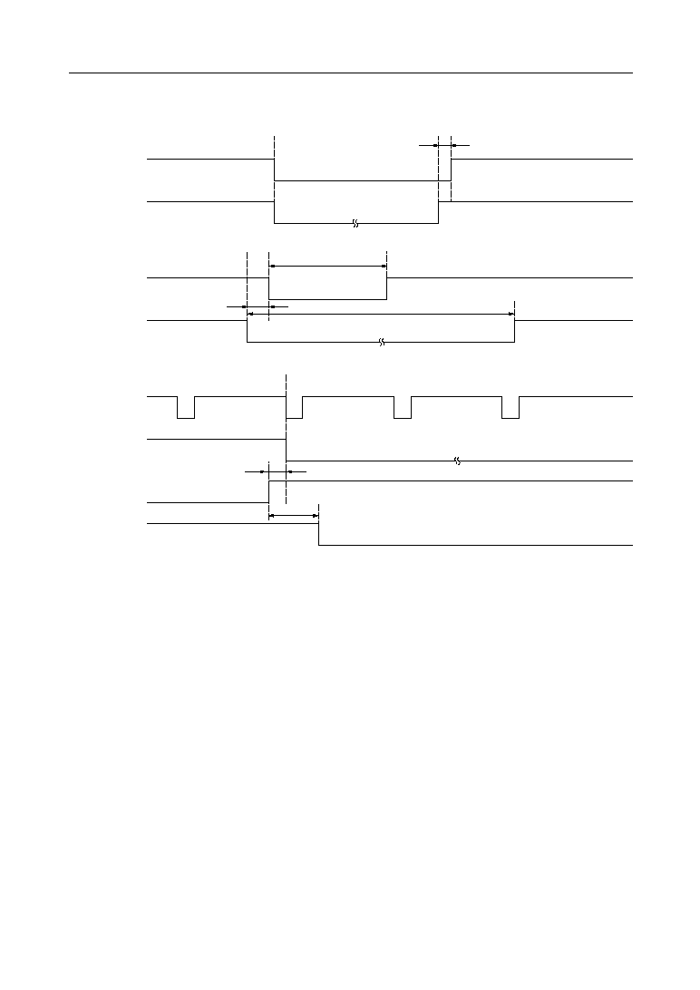
∑ ITU-RBT.656 output
4T
Digital line {1716T (NTSC, 525), 1728T (PAL, 625)}
Digital active line
Digital line blanking
276T (NTSC, 525)
288T (PAL, 625)
Multiplexed video data
Cb0 Y00 Cr0 Cb1 Y10 Cr1 Y11
Video data block (1440T)
EAV
4T
SAV
EAV
T
SAV
EAV
: clock periods 37 ns normal (1/27 MHz)
: start of active video timing reference code
: end of active video timing reference code
ITU-RBT.656 Output (Data in one line in which video data presents)
During the blanking interval, data is output with the Y value.
Note:
Digital line 1716T (NTSC, 525) and 1728T (PAL, 625) are not maintained at the next line.
Digital active line 1440T of the line immediately after VVALID falls and the 10th or 11th
line after VSYNC_L rises will fluctuate due to pixel compensation. Especially when a
non-standard signal is input, the line immediately after VVALID falls will fluctuate
largely due to instability of the input signal. Due to phenomena such as an increase in
the number of lines for a standard signal and a decrease in the number of lines for a non-
standard signal, it may not be possible to guarantee correct EAV and SAV functionality.
° Semiconductor
MSM7662
28/62
PEDL7662-02
Contents of SAV and EAV
Both SAV and EAV consist of 4 words. Their configuration is shown below.
Word
Bit No.
F = 0: during field 1
1: during field 2
V = 0: elsewhere
1: during field blanking
H = 0: SAV H = 1: EAV
7 (MSB)
6
5
4
3
2
1
0 (LSB)
First
1
1
1
1
1
1
1
1
Second
0
0
0
0
0
0
0
0
Third
0
0
0
0
0
0
0
0
Fourth
P3, P2, P1, P0: Protection bit
1
F
V
H
P3
P2
P1
P0
The 4th word of SAV and EAV
The relationship between the F, V, H and Protection bits in the 4th word of SAV and EAV
is shown below.
Bit No.
7 (MSB)
6
5
4
3
2
1
0
Function
Fixed 1
F
V
H
P3
P2
P1
P0
0
1
0
0
0
0
0
0
0
1
1
0
0
1
1
1
0
1
2
1
0
1
0
1
0
1
1
3
1
0
1
1
0
1
1
0
4
1
1
0
0
0
1
1
1
5
1
1
0
1
1
0
1
0
6
1
1
1
0
1
1
0
0
7
1
1
1
1
0
0
0
1
Usually, V = 1 during blanking, however when VBI data is detected and V = 0 is the desired
output, set the MRC[3] SAV, EAV V-status of Mode Register C (MRC) to "1".
° Semiconductor
MSM7662
29/62
PEDL7662-02
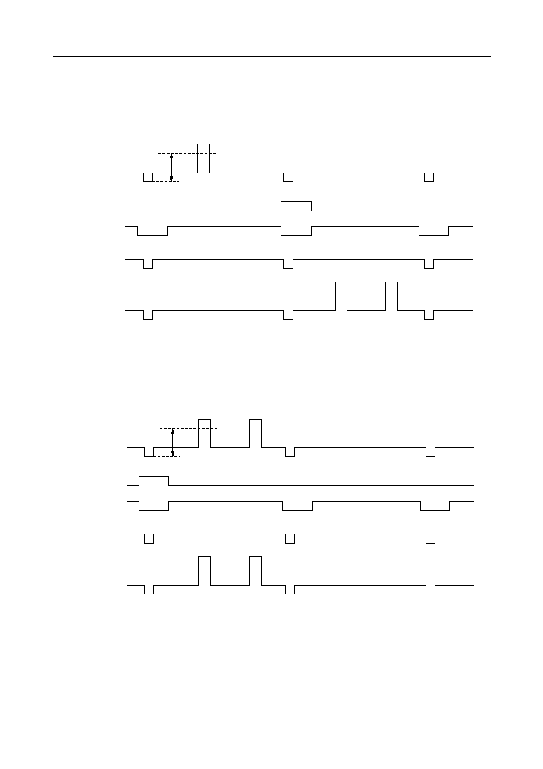
Cb0
Y[7:0]
HVALID
CLKX2
Y0 Cr0 Y1 Cb2 Y2 Cr2 Y3 Cb4
Cr n≠4 Y n≠3 Cb n≠2 Y n≠2 Cr n≠2 Y n≠1
8-bit (YCbCr: 2x clock) Output
Y0
Y1
Y2
Y3
Y(n≠2)
Y(n≠1)
Y[7:0]
HVALID
CLKO
CLKX2
Cb0
Cr0
Cb2
Cr2
Cb(n≠2) Cr(n≠2)
C(7:0)
16-bit (Y: 8-bit, CbCr: 8-bit) Output
R0
R1
R2
R3
R(n≠2)
R(n≠1)
R[7:0]
HVALID
CLKO
CLKX2
G0
G1
Cb2
Cr3
G(n≠2)
G(n≠1)
G[7:0]
B0
B1
B2
B3
B(n≠2)
B(n≠1)
B[7:0]
24-bit (R: 8-bit, G: 8-bit, B: 8-bit) Output
Output Data Format
Note:
When a single-speed clock (13.5 MHz, etc.) is input in 16-bit or 24-bit (RGB) output
mode, the waveform of CLKX2 changes to a single speed waveform, but the format
after that is not changed.
° Semiconductor
MSM7662
30/62
PEDL7662-02
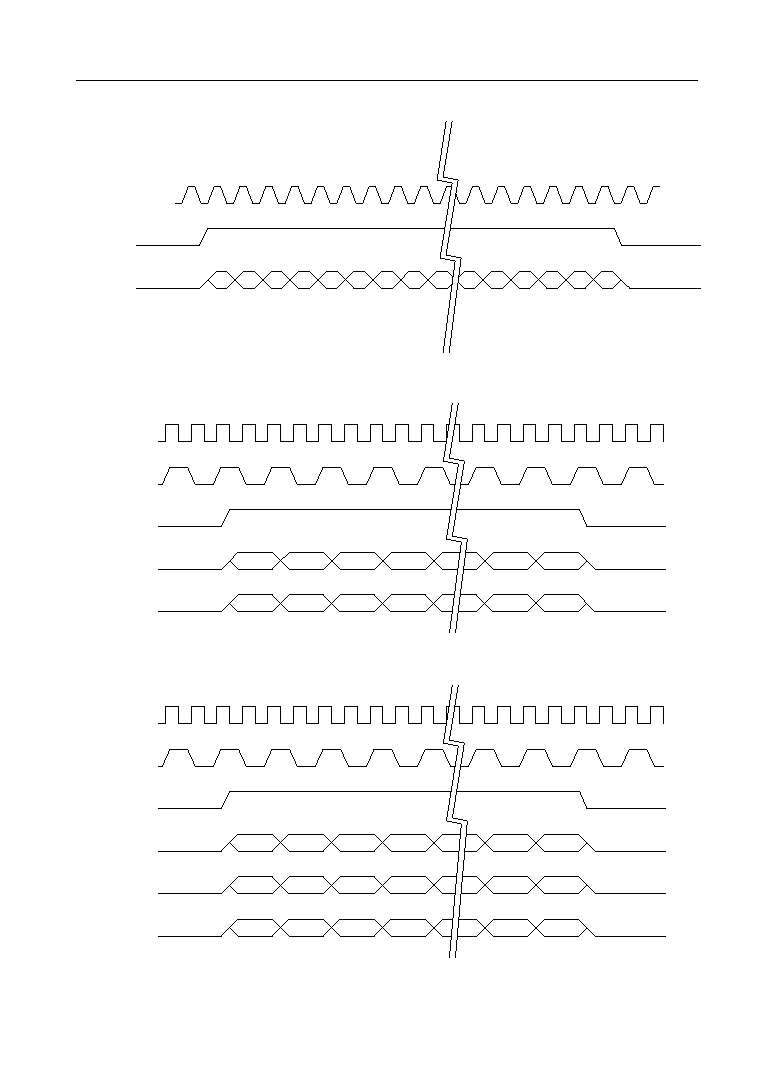
∑ Timing when using external field memory
Field memory timing in the FM-2 mode, using control signals from the decoder
Field memory: MSM51V8222, 2 units are used (Y and C)
Four memory control signals are supplied from the decoder, M[4]: RSTW, M[5]: RSTR, M[6]:
WE:, and M[7]: RE.
NTSC Signal (13.5 MHz)
hsync_l
1
35
2 3 4 5 6 7 8 9 10 11 12 13 14 15 16 17 18 19 20 21 22 23 24 25 26 27 28 29 30 31 32 33 34
vsync_l
hvalid
vvalid
odd-even
y (7:0)
c (7:0)
RSTW
WE
HSYNC_L
VSYNC_L
HVLID
VVALID
ODD/EVEN
RE
RSTR
Y (7:0)
C (7:0)
NTSC: ODD Field
hsync_l
1
35
2 3 4 5 6 7 8 9 10 11 12 13 14 15 16 17 18 19 20 21 22 23 24 25 26 27 28 29 30 31 32 33 34
vsync_l
hvalid
vvalid
odd-even
y (7:0)
c (7:0)
RSTW
WE
HSYNC_L
VSYNC_L
HVLID
VVALID
ODD/EVEN
RE
RSTR
Y (7:0)
C (7:0)
NTSC: EVEN Field
° Semiconductor
MSM7662
31/62
PEDL7662-02
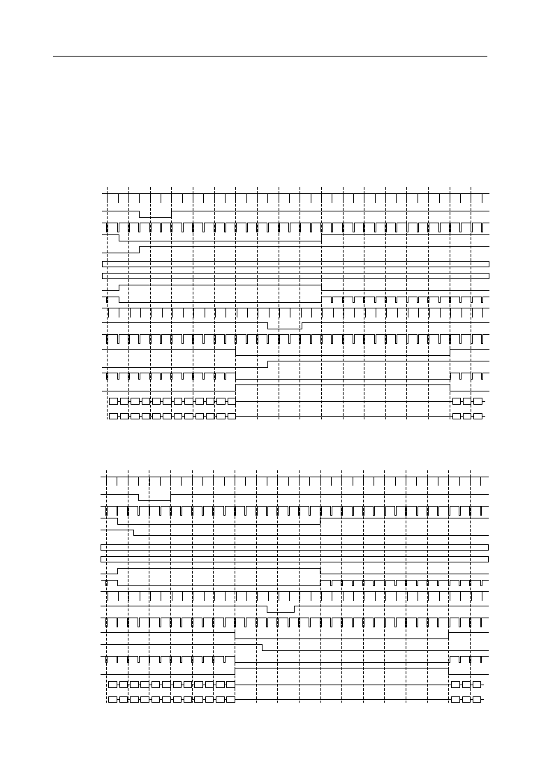
PAL Signal (13.5 MHz)
hsync_l
1
39
2 3 4 5 6 7 8 9 10 11 12 13 14 15 16 17 18 19 20 21 22 23 24 25 26 31 32 33 34 35 36 37 38
vsync_l
hvalid
vvalid
odd-even
y (7:0)
c (7:0)
RSTW
WE
HSYNC_L
VSYNC_L
HVLID
VVALID
ODD/EVEN
RE
RSTR
Y (7:0)
C (7:0)
PAL: ODD Field
hsync_l
1
38
2 3 4 5 6 7 8 9 10 11 12 13 14 15 16 17 18 19 20 21 22 23 24 25 26 27 31 32 33 34 35 36 37
vsync_l
hvalid
vvalid
odd-even
y (7:0)
c (7:0)
RSTW
WE
HSYNC_L
VSYNC_L
HVLID
VVALID
ODD/EVEN
RE
RSTR
Y (7:0)
C (7:0)
PAL: EVEN Field
° Semiconductor
MSM7662
32/62
PEDL7662-02
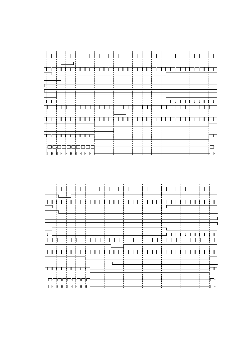
Horizontal Synchronizing Signal
The horizontal synchronizing signal timing is shown below.
Y[7:0]
HVALID
HSYNC_L
60 pixels
Front-porch
Hsync back-porch
Relation between Video Mode and Pixel Number (default settings when standard signal is input)
Video
Mode
Pixel
Type
Pixel Rate
(MHz)
Total
Pixels
Active
Pixels
Front-
Porch
Hsync Back-
Porch
HBLK
Total
ITURBT.601
13.5
858
720
16
122
138
NTSC
Square pixel
12.272727
780
640
28
112
140
4fsc
14.31818
910
768
8
134
142
PAL
ITURBT.601
13.5
864
720
12
132
144
Square pixel
14.75
944
768
34
142
176
Horizontal Timing
° Semiconductor
MSM7662
33/62
PEDL7662-02
HVALID
VVALID
0
2T
T = 1/13.5 MHz
HSYNC_L
HVALID
138 pixels
60 pixels
16 pixels
HSYNC_L
VSYNC_L
ODD
(ODD)
ODD
(EVEN)
0
about 10.4
ms
about 21.6
ms
Synchronizing Signal Timing (default timing when standard signal is input)
° Semiconductor
MSM7662
34/62
PEDL7662-02
VBI Data Detection (when an S-Video signal is input): STATUS1 Timing
VBI data detection results are output from the STATUS1 pin.
video in
Y[7:0]
HSYNC_L
HVALID
STATUS1
Detection level
OMR[5:3]
80 to 136
VBI Data Detection (when a Composite signal is input): STATUS1 Timing
VBI data detection results are output from the STATUS1 pin.
video in
Y[7:0]
HSYNC_L
HVALID
STATUS1
Detection level
OMR[5:3]
80 to 136
° Semiconductor
MSM7662
35/62
PEDL7662-02
I
2
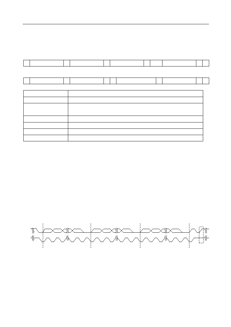
C BUS FORMAT
The I
2
C-bus interface input format is shown below.
S
Slave Address
A
Subaddress
Data n
Description
Start condition
Slave address 1000001X, 8th bit is write signal ["0"] or read signal ["1"]
Slave address is set at M[2] pin (pin 89).
Acknowledge. Generated by slave
Subaddress byte
Data to write to address designated by subaddress.
Symbol
P
Stop condition
Slave Addres (W)
S
Subaddress
A
Slave Addres (R)
A
A
Data 20
A
P
Read Mode
Slave Addres (W)
S
Subaddress
A
Data 0
A
A
......
Data n
A
P
Write Mode
S
As mentioned above, the write operation can be executed from subaddress to subaddress
continuously. When the write operation is executed at subaddresses discontinuously, the
Acknowledge and Stop condition formats are input repeatedly after Data 0.
Data can be read at subaddress 0x20 only.
If one of the following matters occurs, the decoder will not return "A" (Acknowledge).
∑ The slave address does not match.
∑ A non-existent subaddress is specified.
∑ The write attribute of a register does not match "X" (read ["1"]/write ["0"] control bit).
The input timing is shown below.
S
Start Condition
P
SCL
SDA
2
1
8
ACK
Sub Address
2
1
8
ACK
Data
2
1
8
ACK
Stop Condition
Slave Address
° Semiconductor
MSM7662
36/62
PEDL7662-02
OPERATING MODE SETTING
There are two types of video mode settings.
1. External pin mode: direct setting from dedicated pins
2. Register setting mode: specification by internal register settings
These modes can be switched by the mode register MRA[0].
The reset state (default) is the external pin mode.
The following registers can be set in the external pin mode.
MRA[7:6]
Output mode
00: ITU-RBT.656 (SAV, EAV, blank processing)
*01: 8 bit (YCbCr)
HSYNC_L and VSYNC_L used for synchronization
10: ITU-RBT.601 16 bit (8 bit Y, 8 bit CbCr)
11: RGB (8 bit R, 8 bit G, 8 bit B)
MRA[3:1]
Sampling mode
*000: NTSC ITU-RBT.601
13.5 MHz (27.0 MHz)
001: NTSC Square Pixel 12.272727 MHz (24.545454 MHz)
010: NTSC 4fsc
14.31818 MHz (28.63636 MHz)
100: PAL ITU-RBT.601
13.5 MHz (27.0 MHz)
101: PAL Square Pixel
14.75 MHz (29.5 MHz)
Note:
010: NTSC 4fsc cannot be set externally.
Pin Setting Example
NTSC, 27 MHz (ITU-RBT.601), Composite input, 8-bit (YCbCr) Output
Notes
Condition
Pin name
0 : ITU-RBT.656 01 : 8-bit (YCbCr)
= low
MODE[3]
10 : 16-bit (Y + CbCr) 11 : RGB
= high
MODE[2]
0 : NTSC 1 : PAL
= low
MODE[1]
0 : ITU-RBT.601 1 : Square Pixel
= low
MODE[0]
0 : twice the pixel frequency 1 : pixel frequency
= low
CLKSEL
= low
PLLSEL
= low
INS[2:0]
Normally set to a low level
= low
GAINS[2:0]
= low
TEST[2:0]
= low
SCAN
= low
M[2]
Normally set to a low level
= low
M[1]
= low
M[0]
0 : normal operation 1 : sleep operation
= low
SLEEP
: low = 1000001, : high = 1000011
° Semiconductor
MSM7662
37/62
PEDL7662-02
INTERNAL REGISTERS
Register List
D7
MRA7
MRB7
HSYT7
D6
D5
D4
Data byte
D3
D2
D1
D0
Sub-
address
Register Function
Mode Register A (MRA)
Mode Register B (MRB)
Horizontal Sync Trimmer (HSYT)
STHR7
Sync Threshold Level Adjust (STHR)
HSDL7
Horizontal Sync Delay (HSDL)
HVALID7
Horizontal Valid Trimmer (HVALT)
VVALID7
Vertical Valid Trimmer (VVALT)
LUMC7
Luminance Control (LUMC)
AGCLF7
AGC/Pedestal Loop Filter Control (AGCLF)
SSEPL7
Sync Separation Level (SSEPL)
CHRC7
Chrominance Control (CHRC)
ACCLF7
ACC Loop Filter Control (ACCLF)
HUE7
Hue Control (HUE)
OMR7
Output Phase Control for Data Y (OPCY)
MRA6
MRB6
HSYT6
STHR6
HSDL6
HVALID6
VVALID6
LUMC6
AGCLF6
SSEPL6
CHRC6
ACCLF6
HUE6
OMR6
MRA5
MRB5
HSYT5
STHR5
HSDL5
HVALID5
VVALID5
LUMC5
AGCLF5
SSEPL5
CHRC5
ACCLF5
HUE5
OMR5
MRA4
MRB4
HSYT4
STHR4
HSDL4
HVALID4
VVALID4
LUMC4
AGCLF4
SSEPL4
CHRC4
ACCLF4
HUE4
OMR4
MRA3
MRB3
HSYT3
STHR3
HSDL3
HVALID3
VVALID3
LUMC3
AGCLF3
SSEPL3
CHRC3
ACCLF3
HUE3
OMR3
MRA2
MRB2
HSYT2
STHR2
HSDL2
HVALID2
VVALID2
LUMC2
AGCLF2
SSEPL2
CHRC2
ACCLF2
HUE2
OMR2
MRA1
MRB1
HSYT1
STHR1
HSDL1
HVALID1
VVALID1
LUMC1
AGCLF1
SSEPL1
CHRC1
ACCLF1
HUE1
OMR1
MRA0
MRB0
HSYT0
STHR0
HSDL0
HVALID0
VVALID0
LUMC0
AGCLF0
SSEPL0
CHRC0
ACCLF0
HUE0
OMR0
0
1
2
3
4
5
6
7
8
9
A
B
C
D
OPCC7
Output Phase Control for Data C (OPCC)
OPCC6 OPCC5 OPCC4 OPCC3 OPCC2 OPCC1 OPCC0
E
F
Write
Write
Write
Write
Write
Write
Write
Write
Write
Write
Write
Write
Write
Write
Write
Write
Write
/Read
ADC17
Optional Mode Register (OMR)
10
Write
ADC27
ADC Register (ADC1)
11
Write
ADC37
ADC Register (ADC2)
12
Write
ZLD7
ADC Register (ADC3)
13
Write
STATUS7
Stataus Register (STATUS)
20
Read
0 Level Detect Register (ZLD)
14
Write
Mode Register C (MRC)
MRC7 MRC6 MRC5 MRC4 MRC3 MRC2 MRC1 MRC0
OPCY7 OPCY6 OPCY5 OPCY4 OPCY3 OPCY2 OPCY1 OPCY0
ADC16
ADC26
ADC36
ZLD6
STATUS6
ADC15
ADC25
ADC35
ZLD5
STATUS5
ADC14
ADC24
ADC34
ZLD4
STATUS4
ADC13
ADC23
ADC33
ZLD3
STATUS3
ADC12
ADC22
ADC32
ZLD2
STATUS2
ADC11
ADC21
ADC31
ZLD1
STATUS1
ADC10
ADC20
ADC30
ZLD0
STATUS0

° Semiconductor
MSM7662
38/62
PEDL7662-02
Register Parameters
Registers controlled from the I
2
C-bus are listed below.
An asterisk (*) indicates that the register setting value is the default value.
Mode Register A (MRA)
Write only
<address: $00>
MRA[7:6]
Video output mode
00: ITU-RBT.656
*01: Y, C 8 bits
10: Y, C 16 bits
11: RGB 24 bits
Video output mode is selected.
MRA[5]
Chroma format
*0: Offset binary
1: 2's complement
MRA[4]
Undefined
Set to 0
1: S-video input
MRA[3:1]
Input Sampling mode
*000: NTSC ITU-RBT.601
13.5 MHz
001: NTSC Square Pixel
12.272727 MHz
010: NTSC 4fsc
14.31818 MHz
100: PAL ITU-RBT.601
13.5 MHz
101: PAL Square Pixel
14.75 MHz
110, 111: Undefined
Sampling rate is selected
MRA[0]
MODE[3:0] pin select
*0: External pin mode
1: Register mode
Note:
Only the setting of MODE[3:0] is valid in this external pin mode.
Register Name
Default
Recommended Value
MRA[7] MRA[6] MRA[5] MRA[4] MRA[3] MRA[2] MRA[1] MRA[0]
0
--
1
--
0
--
0
0
0
--
0
--
0
--
0
--

° Semiconductor
MSM7662
39/62
PEDL7662-02
MRB[7:6]
Synchronization mode
*00: FIFO-1 (use internal memory)
01: FIFO-2 (use internal memory)
10: FM-1 (use external memory, external control)
11: FM-2 (use external memory, control signals
supplied from M[7:4])
Note:
In the FIFO-1 mode, the number of pixels per 1H is output at the standard setting value.
In the FIFO-2 mode, the number of pixels per 1H is fixed in accordance with an input
H period and output.
In the FM-1 and FM-2 modes, a decoded result is output without any changes
according to the SYNC signal. A field memory is required externally to output the fixed
number of pixels in those modes. In the FM-2 mode, a field memory control signal is
output from the pin M[7:4].
MRB[5]
Color killer mode
*0: Auto color killer (Chrominance signal level is
set to "0" if the color burst level is below the
specified value.)
*1: Forced color killer (Chrominance signal level
is forced to "0".)
MRB[4]
Blue Back
0: OFF (Video signal is demodulated and output
regardless of synchronization detection.)
*1: AUTO (Blue Back is output when synchro-
nization is not detected.)
Note:
When Blue Back output is selected, if "H" level is not input during no signal output, a
vertical synchronizing signal (VSYNC_L) is not output.
MRB[3:2]
Clamp mode
*00: Analog clamp
01: Analog, Digital hybrid clamp
10: Digital clamp (HSY clamp)
11: Undefined
Clamp mode is selected.
MRB[1:0]
Y/C separation mode
*00: Adaptive comb filter (Correlation of 3 lines is
monitored and operating mode is selected.)
01: Non-adaptive comb filter (Operating mode is
always fixed.)
10: Use trap filter. (Comb filter is not used.)
11: Undefined
Note: Adaptive comb filter
2/3-line comb filter for NTSC
Comb filter/trap filter for PAL
Non-adaptive comb filter
3-line comb filter for NTSC
2-line cosine comb filter for PAL
Register Name
Default
Recommended Value
MRB[7] MRB[6] MRB[5] MRB[4] MRB[3] MRB[2] MRB[1] MRB[0]
0
0
0
0
0
0
1
1
0
0
0
0
0
0
0
0
Mode Register B (MRB)
Write only
<address: $01>
° Semiconductor
MSM7662
40/62
PEDL7662-02
STHR[7:0]
Sync. depth
$00 to $FF (*$1E): 0 to 255
Note:
The STHR signal changes the HSYNC_L detection level. The numerical unit described
here is determined based on 80IRE obtained from doubling the pedestal value of
standard signal, if set to 40IRE. For example, the default 0x1E is 30 in digital value,
which is reduced to 15IRE.
Register Name
Default
Recommended Value
STHR[7] STHR[6] STHR[5] STHR[4] STHR[3] STHR[2] STHR[1] STHR[0]
0
0
0
0
0
1
1
1
1
0
1
1
1
1
0
1
HSYT[7:4]
HSY start trimmer (• 8 pixels)
$C to $B (*$0): ≠4 to +11 (≠32 to +88 pixels)
HSYT[3:0]
HSY stop trimmer (• 8 pixels)
$C to $B (*$0): ≠4 to +11 (≠32 to +88 pixels)
Note:
The HSYT signal provides the clamp timing to the A/D converter during digital clamp
or hybrid clamp mode. Because this signal can move to the pedestal position, the
pedestal clamp can be used. However, this signal can not be observed from outside.
Sync. Threshold level adjust (STHR) Write only
<address: $04>
Register Name
Default
Recommended Value
HSYT[7] HSYT[6] HSYT[5] HSYT[4] HSYT[3] HSYT[2] HSYT[1] HSYT[0]
0
0
0
0
0
0
0
0
0
0
0
0
0
0
0
0
MRC[7]
NTSC/PAL auto select
0: Fix
*1: Auto
Note:
This register decides automatically when the sampling frequency of input signals is
ITU-RBT.601.
MRC[6]
Sub pixel alignment
*0: Use pixel position compensating circuit.
1: Do not use pixel position compensating circuit.
MRC[5]
Pixel sampling rate
*0: (4:2:2)
1: (4:1:1)
MRC[4]
Data-pass control
*0: Use DECIMATOR at 2x sampling.
1: Do not use DECIMATER.
Note: This register is valid when a 2x clock (27 MHz) is input.
MRC[3]
SAV, EAV V-status
*0: During blanking, V = 1
1: During blanking, while VBI data is not
detected, V = 1
MRC[2]
RGB output level
*0: 0 to 255
1: 16 to 235
MRC[1:0]
Undefined
Set to 0
Horizontal Sync Trimmer (HSYT)
Write only
<address: $03>
Register Name
Default
Recommended Value
MRC[7] MRC[6] MRC[5] MRC[4] MRC[3] MRC[2] MRC[1] MRC[0]
1
1
0
0
0
--
0
0
0
--
0
--
0
0
0
0
Mode Register C (MRC)
Write only
<address: $02>
° Semiconductor
MSM7662
41/62
PEDL7662-02
HVALT[7:4] HVALID start trimmer (• 2 pixels) $8 to $7 (*$0): ≠8 to +7 (≠16 to +14 pixels)
HVALT[3:0] HVALID stop trimmer (• 2 pixels) $8 to $7 (*$0): ≠8 to +7 (≠16 to +14 pixels)
Note:
HVALID start position and end position are changed.
Vertical Valid Trimmer (VVALT)
Write only
<address: $07>
VVALT[7:4] VVALID start trimmer (• 1 line)
$8 to $7 (*$0): ≠8 to +7
VVALT[3:0] VVALID stop trimmer (• 1 line)
$8 to $7 (*$0): ≠8 to +7
Note:
VVALID start position and end position are changed.
Register Name
Default
Recommended Value
VVALT
VVALT
VVALT
VVALT
VVALT
VVALT
VVALT
VVALT
0
0
0
0
0
0
0
0
0
0
0
0
0
0
0
0
[7]
[6]
[5]
[4]
[3]
[2]
[1]
[0]
Register Name
Default
Recommended Value
HVALT
HVALT
HVALT
HVALT
HVALT
HVALT
HVALT
HVALT
0
0
0
0
0
0
0
0
0
0
0
0
0
0
0
0
[7]
[6]
[5]
[4]
[3]
[2]
[1]
[0]
HSDL[7:0]
HSYNC_L delay trimmer (• 1 pixel)
$80 to $7F (*$00): ≠128 to +127 (≠128 to +127
pixels)
Note:
The HSYNC_L sync signal output position is adjusted.
Horizontal Valid Trimmer (HVALT) Write only
<address: $06>
Horizontal Sync Delay (HSDL)
Write only
<address: $05>
Register Name
Default
Recommended Value
HSDL[7] HSDL[6] HSDL[5] HSDL[4] HSDL[3] HSDL[2] HSDL[1] HSDL[0]
0
0
0
0
0
0
0
0
0
0
0
0
0
0
0
0
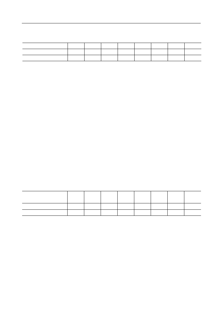
° Semiconductor
MSM7662
42/62
PEDL7662-02
LUMC[7]
Output level limiter
*0: OFF
1: ON
Note: Control range while limiter is ON: 16 to 235
LUMC[6]
Use of prefilter
*0: Do not use prefilter.
1: Use prefilter.
LUMC[5:4]
Aperture bandpass select
*00: range0 (middle)
01: range1
10: range2
11: range3 (high)
LUMC[3:2]
Coring range select
*00: coring off
01:
±
4LSB
10:
±
5LSB
11:
±
7LSB
LUMC[1:0]
Aperture filter weighting factor
*00: 0.00
01: 0.25
10: 0.75
11: 1.50
Note:
These registers are used for contour compensation.
AGC/Pedestal Loop filter control (AGCLF)
Write only
<address: $09>
AGCLF[7:6] AGC loop filter time constant
00: slow
*01: medium
10: fast
11: MGC mode
Note:
The AGC convergence time is determined. These registers converge about 4 times
faster by slow-medium-fast steps. In the MGC mode, the amplification is determined
by reference level.
AGCLF[5:0] AGC reference level
$20 to $1F (*$00): ≠32 to +31
Register Name
Default
Recommended Value
AGCLF
AGCLF
AGCLF
AGCLF
AGCLF
AGCLF
AGCLF
AGCLF
0
0
1
1
0
0
0
0
0
0
0
0
0
0
0
0
[7]
[6]
[5]
[4]
[3]
[2]
[1]
[0]
Luminance Control (LUMC)
Write only
<address: $08>
Register Name
Default
Recommended Value
LUMC[7] LUMC[6] LUMC[5] LUMC[4] LUMC[3] LUMC[2] LUMC[1] LUMC[0]
0
0
0
0
0
0
0
0
0
0
0
0
0
0
0
0
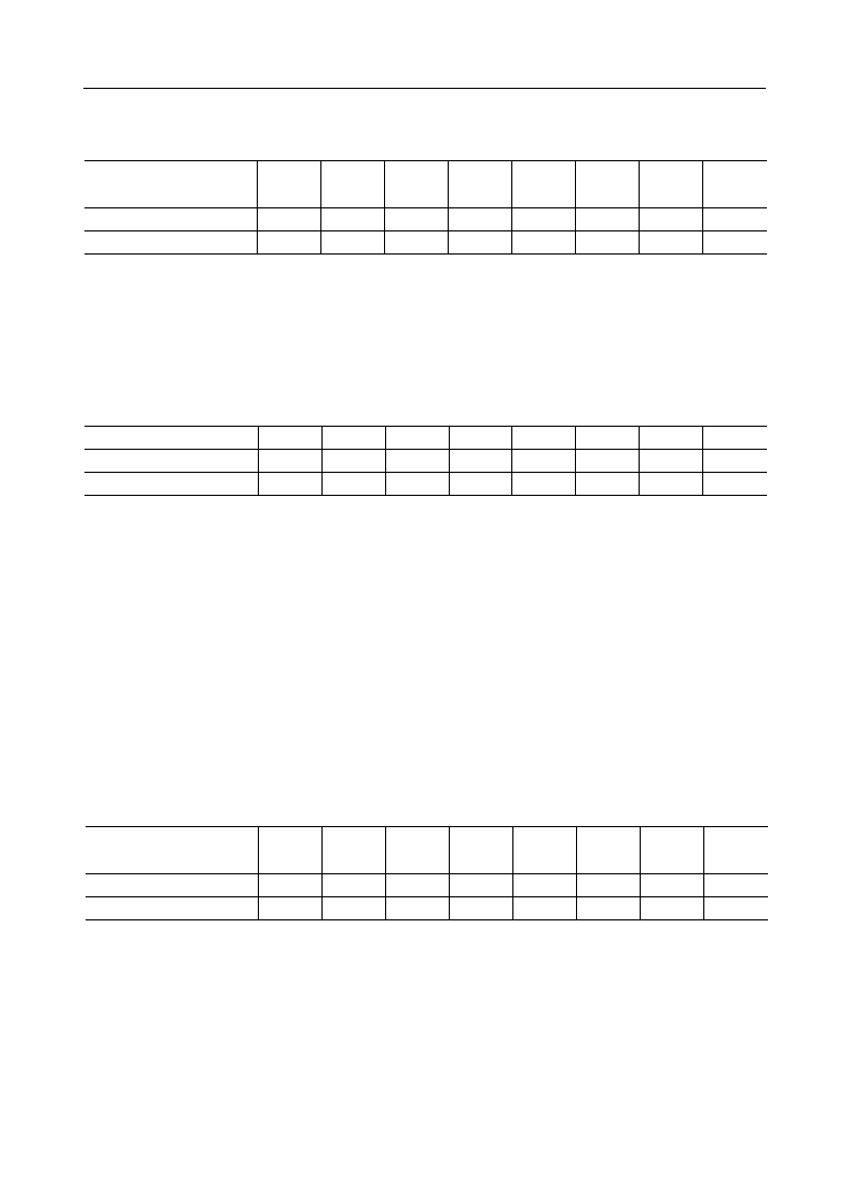
° Semiconductor
MSM7662
43/62
PEDL7662-02
ACCLF[7]
Undefined
Set to 0
ACCLF[6:5] ACC loop filter time constant
00: slow
*01: medium
10: fast
11: MCC mode
Note:
The ACC convergence time is determined. These registers converge about 4 times
faster by slow-medium-fast steps. In the MCC mode, the amplification is determined
by reference level.
ACCLF[4:0] ACC reference level
$10 to $0F (*$00): ≠16 to +15
Register Name
Default
Recommended Value
ACCLF
ACCLF
ACCLF
ACCLF
ACCLF
ACCLF
ACCLF
ACCLF
0
0
0
0
1
1
0
0
0
0
0
0
0
0
0
0
[7]
[6]
[5]
[4]
[3]
[2]
[1]
[0]
CHRC[7:4]
Undefined
Set to 0
CHRC[3]
C-Output level limiter
*0: OFF
1: ON
Note: Control range while limiter is ON: 16 to 224
CHRC[2]
Chroma bandpass filter
0: OFF
*1: ON
CHRC[1:0]
Color kill threshold factor
00: 0.500 color burst level
*01: 0.250 color burst level
10: 0.125 color burst level
11: Color killer off
Note:
The color killer decision level is selected based upon color burst ratio.
ACC Loop filter control (ACCLF)
Write only
<address: $0C>
Register Name
Default
Recommended Value
CHRC[7] CHRC[6] CHRC[5] CHRC[4] CHRC[3] CHRC[2] CHRC[1] CHRC[0]
0
0
0
0
0
0
0
0
0
0
1
1
0
0
1
1
SSEPL[7]
Pedestal Clamp on/off
*0: Do not use pedestal clamp.
1: Use pedestal clamp (AGC stops operating).
SSEPL[6:0]
Sync. separation level
$40 to $3F (*$00): ≠64 to +63
Note:
The default setting outputs the pedestal position as a black level.
Chrominance Control (CHRC) Write only
<address: $0B>
Register Name
Default
Recommended Value
SSEPL
SSEPL
SSEPL
SSEPL
SSEPL
SSEPL
SSEPL
SSEPL
0
0
0
0
0
0
0
0
0
0
0
0
0
0
0
0
[7]
[6]
[5]
[4]
[3]
[2]
[1]
[0]
Sync separation level (SSEPL) Write only
<address: $0A>
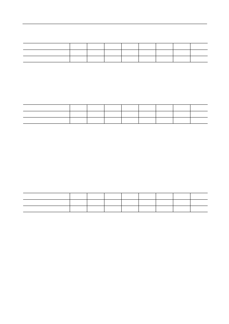
° Semiconductor
MSM7662
44/62
PEDL7662-02
OPCC[7:2]
Undefined
Set to 0
OPCC[1:0]
Output phase control for data C
*00: normal
01: forward l clock
10: backward 2 clock
11: backward l clock
Note:
The output phase of data C is controlled.
Register Name
Default
Recommended Value
OPCC[7] OPCC[6] OPCC[5] OPCC[4] OPCC[3] OPCC[2] OPCC[1] OPCC[0]
0
0
0
0
0
0
0
0
0
0
0
0
0
0
0
0
OPCY[7:2]
Undefined
Set to 0
OPCY[1:0]
Output phase control for data Y
*00: normal
01: forward l clock
10: backward 2 clock
11: backward l clock
Note:
The output phase of data Y is controlled.
Output phase control for data C (OPCC)
Write only
<address: $0F>
Register Name
Default
Recommended Value
OPCY[7] OPCY[6] OPCY[5] OPCY[4] OPCY[3] OPCY[2] OPCY[1] OPCY[0]
0
0
0
0
0
0
0
0
0
0
0
0
0
0
0
0
Hue control (HUE)
Write only
<address: $0D>
Register Name
Default
Recommended Value
HUE[7]
HUE[6]
HUE[5]
HUE[4]
HUE[3]
HUE[2]
HUE[1]
HUE[0]
0
0
0
0
0
0
0
0
0
0
0
0
0
0
0
0
HUE[7:0]
Hue control
$80 to $7F (*$00): ≠180 to +178.6 degrees
Note:
The phase is controlled. It changes about 1.4 degrees per bit.
Output phase control for data Y (OPCY)
Write only
<address: $0E>

° Semiconductor
MSM7662
45/62
PEDL7662-02
OMR[7]
HSYNC output timing select *0: HSYNC output signal is detected near sync
threshold and sync tip.
1: HSYNC output signal is detected at sync
threshold setting position.
Note:
When the HSYNC output signal is detected at sync threshold setting position, it is
hardly affected by noise.
OMR[6]
VSYNC output timing select *0: VSYNC_L is synchronized to HSYNC_L and
then output
1: VSYNC_L is output when a VSYNC input
signal is detected.
Note:
When a non-standard signal is decoded, the output is stabilized after the VSYNC_L
input signal is detected (setting 1).
OMR[5:3]
Multiplex signal detection level
(VBID etc.)
000: 80
001: 88
*010: 96
011: 104
100: 112
101: 120
110: 128
111: 136
Note:
The levels to detect multiplexed signals sent during the vertical blanking period are set.
The result is output from the STATUS[1] pin or STATUS[4] register.
OMR[2]
Hi-Z output in SLEEP mode
*0: Active
1: Hi-Z
Note:
This register selects either normal or Hi-Z as the output pin status in SLEEP mode.
OMR[1]
Status2 output mode
*0: NTSC/PAL identification
1: HLOCK sync detection
OMR[0]
Status3 output mode
*0: TV/VCR identification
1: CSYNC
Note:
OMR[1:0] correspond to the STATUS[2:3] output of output pins.
Register Name
Default
Recommended Value
OMR[7] OMR[6] OMR[5] OMR[4] OMR[3] OMR[2] OMR[1] OMR[0]
0
1
0
1
0
0
1
1
0
0
0
0
0
0
0
0
Optional Mode Register (OMR)
Write only
<address: $10>
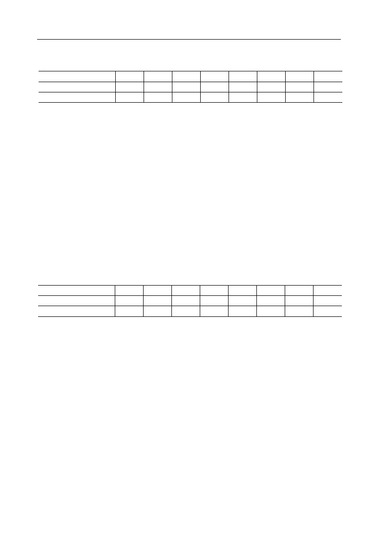
° Semiconductor
MSM7662
46/62
PEDL7662-02
ADC1[7]
Video amp select
*0: Use
1: Do not use
ADC1[6]
Undefined
Set to 0
ADC1[5:4]
Clamp current select
*00: 1.0
01: 0.75
10: 0.25
11: 0.1
ADC1[3]
Undefined
Set to 0
ADC1[2:0]
ADC input select
*000: ADI-VIN1 (composite-1)
001: ADI-VIN2 (composite-2)
010: ADI-VIN3 (composite-3)
011: ADI-VIN4 (composite-4)
100: ADI-VIN5 (composite-5)
101: ADI-VIN1 (Y-1), AD2-VIN5 (C-1)
110: ADI-VIN2 (Y-1), AD2-VIN6 (C-1)
111: Prohibited setting (ADC enters sleep state)
ADC register 2 (ADC2)
Write only
<address: $12>
ADC2[7]
ADC gain control mode select
0: manual
*1: auto
ADC2[6:4]
ADC gain manual select
000: 1.00
*001: 1.35
010: 1.75
011: 2.30
100: 3.00
101: 3.80
110: 5.00
111: Undefined
ADC2[3]
ADC initialize condition gain select
0: not initialize
*1: initialize
ADC[2]
Undefined
Set to 0
ADC2[1:0]
ADC gain control and stage select
00: 2
nd
change end
01: 3
rd
change end
*10: 3
rd
change loop
11: Undefined
Register Name
Default
Recommended Value
ADC1[7] ADC1[6] ADC1[5] ADC1[4] ADC1[3] ADC1[2] ADC1[1] ADC1[0]
0
0
0
0
0
1
0
1
0
0
0
--
0
--
0
--
Register Name
Default
Recommended Value
ADC2[7] ADC2[6] ADC2[5] ADC2[4] ADC2[3] ADC2[2] ADC2[1] ADC2[0]
1
0
0
0
0
0
1
1
1
1
1
1
1
1
0
0
ADC register 1 (ADC1)
Write only
<address: $11>
° Semiconductor
MSM7662
47/62
PEDL7662-02
ZLD[7:3]
Undefined
Set to 0
ZLD[2:0]
0 level detect width (• 8 pixel)
000: Undefined
001: 8 pixels
*010: 16 pixels
011: 24 pixels
100: 32 pixels
101: 40 pixels
110: 48 pixels
111: 56 pixels
Note:
These registers decide the continuance of sync tip level and its result is reflected in AGC
gain. The stability can be obtained from higher values.
Register Name
Default
Recommended Value
ZLD[7]
ZLD[6]
ZLD[5]
ZLD[4]
ZLD[3]
ZLD[2]
ZLD[1]
ZLD[0]
0
0
0
0
0
0
0
0
0
0
0
0
1
1
0
0
ADC3[7]
Undefined
Set to 0
ADC3[6:4]
ADC gain control margin level select
000: 10 mV
001: 20 mV
*010: 40 mV
011: 80 mV
100: 160 mV
ADC3[3]
Undefined
Set to 0
ADC3[2:0]
ADC gain control line select
000: 1 line
001: 2 lines
*010: 4 lines
011: 8 lines
100: 16 lines
Note:
These registers determine the analog gain control decision level. The stability can be
obtained from higher values.
0 level detect register (ZLD)
Write only
<address: $14>
ADC register 3 (ADC3)
Write only
<address: $13>
Register Name
Default
Recommended Value
ADC3[7] ADC3[6] ADC3[5] ADC3[4] ADC3[3] ADC3[2] ADC3[1] ADC3[0]
0
0
0
0
1
1
0
0
0
0
0
0
1
1
0
0

° Semiconductor
MSM7662
48/62
PEDL7662-02
Status register (STATUS)
Read only
<address: $20>
STATUS[7:5] Undefined
STATUS[4]
VBI interval multiplex signal detection
0: Non-detection, 1: Detection
STATUS[3]
HLOCK sync detection
0: Non-detection, 1: Detection
STATUS[2]
NTSC/PAL identification
0: NTSC, 1: PAL
STATUS[1]
Fifo1/Fifo2 identification Mode Register B (bit 6)
0: Fifo1, 1: Fifo2
STATUS[0]
FTFO overflow detection
0: Non-detection, 1: Detection
Register Name
Default
Recommended Value
STATUS STATUS STATUS STATUS STATUS STATUS STATUS STATUS
--
--
--
--
--
--
--
--
--
--
--
--
--
--
--
--
[7]
[6]
[5]
[4]
[3]
[2]
[1]
[0]
° Semiconductor
MSM7662
49/62
PEDL7662-02
Relationship between Register Setting Value and Adjusted Value
Horizontal Sync Trimmer
Position adjustment of sync tip clamp timing signal
HSYT [7:4]
:Adjusting the starting position
Register Setting Value (0x)
Adjusted Value (Pixel)
C
D
E
F
0*
1
2
3
4
5
6
7
8
9
A
B
≠32 ≠24 ≠16 ≠8
0
+8 +16 +24 +32 +40 +48 +56 +64 +72 +80 +88
HSYT [3:0]
:Adjusting the end position
C
D
E
F
0*
1
2
3
4
5
6
7
8
9
A
B
≠32 ≠24 ≠16 ≠8
0
+8 +16 +24 +32 +40 +48 +56 +64 +72 +80 +88
Register Setting Value (0x)
Adjusted Value (Pixel)
Horizontal Sync Delay
Adjustment of the starting position of horizontal sync signal
HSDL [7:0]
Unit: [pixel]
8
9
A
B
C
D
E
F
0*
1
2
3
4
5
6
7
MSB[7 : 4]
≠128 ≠112 ≠96
≠80
≠64
≠48
0
+16
+32
+48
+64
+80
+96 +112
≠127 ≠111 ≠95
≠79
≠63
≠47
+1
≠126 ≠110 ≠94
≠78
≠62
≠46
+2
≠125 ≠109 ≠93
≠77
≠61
≠45
+3
≠124 ≠108 ≠92
≠76
≠60
≠44
+4
≠123 ≠107 ≠91
≠75
≠59
≠43
+5
≠122 ≠106 ≠90
≠74
≠58
≠42
+6
≠121 ≠105 ≠89
≠73
≠57
≠41
+7
≠120 ≠104 ≠88
≠72
≠56
≠40
+8
≠119 ≠103 ≠87
≠71
≠55
≠39
+9
≠118 ≠102 ≠86
≠70
≠54
≠38
+10
≠117 ≠101 ≠85
≠69
≠53
≠37
+11
≠116 ≠100 ≠84
≠68
≠52
≠36
+12
≠115 ≠99
≠83
≠67
≠51
≠35
+13
≠114 ≠98
≠82
≠66
≠50
≠34
+14
≠113 ≠97
≠81
≠65
≠49
≠33
+15
0*
1
2
3
4
5
6
7
8
9
A
B
C
D
E
F
LSB
[3 : 0]
≠32
≠31
≠30
≠29
≠28
≠27
≠26
≠25
≠24
≠23
≠22
≠21
≠20
≠19
≠18
≠17
≠16
≠15
≠14
≠13
≠12
≠11
≠10
≠9
≠8
≠7
≠6
≠5
≠4
≠3
≠2
≠1
+17
+18
+19
+20
+21
+22
+23
+24
+25
+26
+27
+28
+29
+30
+31
+33
+34
+35
+36
+37
+38
+39
+40
+41
+42
+43
+44
+45
+46
+47
+49
+50
+51
+52
+53
+54
+55
+56
+57
+58
+59
+60
+61
+62
+63
+65
+66
+67
+68
+69
+70
+71
+72
+73
+74
+75
+76
+77
+78
+79
+81
+82
+83
+84
+85
+86
+87
+88
+89
+90
+91
+92
+93
+94
+95
+97
+98
+99
+100
+101
+102
+103
+104
+105
+106
+107
+108
+109
+110
+111
+113
+114
+115
+116
+117
+118
+119
+120
+121
+122
+123
+124
+125
+126
+127
Register Setting
Value
(0x)
° Semiconductor
MSM7662
50/62
PEDL7662-02
Horizontal Valid Trimmer
Position adjustment of horizontal valid pixel timing signal
HVALT [7:4]
:Adjusting the starting position
8
9
A
B
C
D
E
F
0*
1
2
3
4
5
6
7
≠16 ≠14 ≠12 ≠10 ≠8
≠6
≠4
≠2
0
+2
+4
+6
+8 +10 +12 +14
Register Setting Value (0x)
Adjusted Value (Pixel)
HVALT [3:0]
:Adjusting the end position
8
9
A
B
C
D
E
F
0*
1
2
3
4
5
6
7
≠16 ≠14 ≠12 ≠10 ≠8
≠6
≠4
≠2
0
+2
+4
+6
+8 +10 +12 +14
Register Setting Value (0x)
Adjusted Value (Pixel)
Vertical Valid Trimmer
Position adjustment of vertical valid line timing signal
VVALT [7:4]
:Adjusting the starting position
VVALT [3:0]
:Adjusting the end position
8
9
A
B
C
D
E
F
0*
1
2
3
4
5
6
7
≠8
≠7
≠6
≠5
≠4
≠3
≠2
≠1
0
+1
+2
+3
+4
+5
+6
+7
Register Setting Value (0x)
Adjusted Value (Line)
8
9
A
B
C
D
E
F
0*
1
2
3
4
5
6
7
≠8
≠7
≠6
≠5
≠4
≠3
≠2
≠1
0
+1
+2
+3
+4
+5
+6
+7
Register Setting Value (0x)
Adjusted Value (Line)
AGC Loop Filter Control
AGCLF [5:0]
:Adjusting AGC sync level
Unit: [IRE], Default: 40 IRE
2
3
0*
1
MSB [5 : 4]
0
+16
+1
+2
+3
+4
+5
+6
+7
+8
+9
+10
+11
+12
+13
+14
+15
1
2
3
4
5
6
7
8
9
A
B
C
D
E
F
LSB
[3 : 0]
≠32
≠31
≠30
≠29
≠28
≠27
≠26
≠25
≠24
≠23
≠22
≠21
≠20
≠19
≠18
≠17
≠16
≠15
≠14
≠13
≠12
≠11
≠10
≠9
≠8
≠7
≠6
≠5
≠4
≠3
≠2
≠1
+17
+18
+19
+20
+21
+22
+23
+24
+25
+26
+27
+28
+29
+30
+31
0*
1
2
3
4
5
6
7
8
9
A
B
C
D
E
F
LSB
Register Setting
Value
(0x)
° Semiconductor
MSM7662
51/62
PEDL7662-02
Sync Separation Level
SSEPL [6:0]
:Adjusting the blanking level
Unit: [IRE], Default: 40 IRE
4
5
6
7
0*
1
2
3
MSB [6 : 4]
≠64
≠48
0
+16
+32
+48
≠63
≠47
+1
≠62
≠46
+2
≠61
≠45
+3
≠60
≠44
+4
≠59
≠43
+5
≠58
≠42
+6
≠57
≠41
+7
≠56
≠40
+8
≠55
≠39
+9
≠54
≠38
+10
≠53
≠37
+11
≠52
≠36
+12
≠51
≠35
+13
≠50
≠34
+14
≠49
≠33
+15
0*
1
2
3
4
5
6
7
8
9
A
B
C
D
E
F
[3 : 0]
≠32
≠31
≠30
≠29
≠28
≠27
≠26
≠25
≠24
≠23
≠22
≠21
≠20
≠19
≠18
≠17
≠16
≠15
≠14
≠13
≠12
≠11
≠10
≠9
≠8
≠7
≠6
≠5
≠4
≠3
≠2
≠1
+17
+18
+19
+20
+21
+22
+23
+24
+25
+26
+27
+28
+29
+30
+31
+33
+34
+35
+36
+37
+38
+39
+40
+41
+42
+43
+44
+45
+46
+47
+49
+50
+51
+52
+53
+54
+55
+56
+57
+58
+59
+60
+61
+62
+63
LSB
LSB
Register Setting
Value
(0x)
° Semiconductor
MSM7662
52/62
PEDL7662-02
ACC Loop Filter Control
ACCLF [4:0]
:Adjusting the color burst level
Unit: [IRE], Default: 40 IRE
1
0*
MSB [4]
0
+1
+2
+3
+4
+5
+6
+7
+8
+9
+10
+11
+12
+13
+14
+15
1
2
3
4
5
6
7
8
9
A
B
C
D
E
F
LSB
[3 : 0]
≠16
≠15
≠14
≠13
≠12
≠11
≠10
≠9
≠8
≠7
≠6
≠5
≠4
≠3
≠2
≠1
0*
1
2
3
4
5
6
7
8
9
A
B
C
D
E
F
LSB
Register Setting
Value
(0x)
° Semiconductor
MSM7662
53/62
PEDL7662-02
Hue Control
Adjustment of color subcarrier phase
HUE [7:0]
Unit: [degree]
8
9
A
B
C
D
E
F
0*
1
2
3
4
5
6
7
MSB [7 : 4]
≠180.0 ≠157.5 ≠135.0 ≠112.5 ≠90.0 ≠67.5
+0.0 +22.5 +45.0 +67.5 +90.0 +112.5 +135.0 +157.5
≠178.6 ≠156.1 ≠133.6 ≠111.1 ≠88.6 ≠66.1
+1.4
≠177.2 ≠154.7 ≠132.2 ≠109.7 ≠87.2 ≠64.7
+2.8
≠175.8 ≠153.3 ≠130.8 ≠108.3 ≠85.8 ≠63.3
+4.2
≠174.4 ≠151.9 ≠129.4 ≠106.9 ≠84.4 ≠61.9
+5.6
≠173.0 ≠150.5 ≠128.0 ≠105.5 ≠83.0 ≠60.5
+7.0
≠171.6 ≠149.1 ≠126.6 ≠104.1 ≠81.6 ≠59.1
+8.4
≠170.2 ≠147.7 ≠125.2 ≠102.7 ≠80.2 ≠57.7
+9.8
≠168.8 ≠146.3 ≠123.8 ≠101.3 ≠78.8 ≠56.3
+11.3
≠167.3 ≠144.8 ≠122.3 ≠99.8 ≠77.3 ≠54.8
+12.7
≠165.9 ≠143.4 ≠120.9 ≠98.4 ≠75.9 ≠53.4
+14.1
≠164.5 ≠142.0 ≠119.5 ≠97.0 ≠74.5 ≠52.0
+15.5
≠163.1 ≠140.6 ≠118.1 ≠95.6 ≠73.1 ≠50.6
+16.9
≠161.7 ≠139.2 ≠116.7 ≠94.2 ≠71.7 ≠49.2
+18.3
≠160.3 ≠137.8 ≠115.3 ≠92.8 ≠70.3 ≠47.8
+19.7
≠158.9 ≠136.4 ≠113.9 ≠91.4 ≠68.9 ≠46.4
+21.1
0*
1
2
3
4
5
6
7
8
9
A
B
C
D
E
F
LSB
[3 : 0]
≠45.0
≠43.6
≠42.2
≠40.8
≠39.4
≠38.0
≠36.6
≠35.2
≠33.8
≠32.3
≠30.9
≠29.5
≠28.1
≠26.7
≠25.3
≠23.9
≠22.5
≠21.1
≠19.7
≠18.3
≠16.9
≠15.5
≠14.1
≠12.7
≠11.3
≠9.8
≠8.4
≠7.0
≠5.6
≠4.2
≠2.8
≠1.4
+23.9
+25.3
+26.7
+28.1
+29.5
+30.9
+32.3
+33.8
+35.2
+36.6
+38.0
+39.4
+40.8
+42.2
+43.6
+46.4
+47.8
+49.2
+50.6
+52.0
+53.4
+54.8
+56.3
+57.7
+59.1
+60.5
+61.9
+63.3
+64.7
+66.1
+68.9
+70.3
+71.7
+73.1
+74.5
+75.9
+77.3
+78.8
+80.2
+81.6
+83.0
+84.4
+85.8
+87.2
+88.6
+91.4
+92.8
+94.2
+95.6
+97.0
+98.4
+99.8
+101.3
+102.7
+104.1
+105.5
+106.9
+108.3
+109.7
+111.1
+113.9
+115.3
+116.7
+118.1
+119.5
+120.9
+122.3
+123.8
+125.2
+126.6
+128.0
+129.4
+130.8
+132.2
+133.6
+136.4
+137.8
+139.2
+140.6
+142.0
+143.4
+144.8
+146.3
+147.7
+149.1
+150.5
+151.9
+153.3
+154.7
+156.1
+158.9
+160.3
+161.7
+163.1
+164.5
+165.9
+167.3
+168.8
+170.2
+171.6
+173.0
+174.4
+175.8
+177.2
+178.6
Register Setting
Value
(0x)

° Semiconductor
MSM7662
54/62
PEDL7662-02
Sync. Threshold Level Adjust
Adjustment of the detection threshold of horizontal sync signal
SHTR [7:0]
Unit: [IRE]/2
0
1*
2
3
4
5
6
7
8
9
A
B
C
D
E
F
MSB [7 : 4]
0
1
2
3
4
5
6
7
8
9
10
11
12
13
14
15
16
17
18
19
20
21
22
23
24
25
26
27
28
29
30
31
32
33
34
35
36
37
38
39
40
41
42
43
44
45
46
47
48
49
50
51
52
53
54
55
56
57
58
59
60
61
62
63
64
65
66
67
68
69
70
71
72
73
74
75
76
77
78
79
80
81
82
83
84
85
86
87
88
89
90
91
92
93
94
95
128
129
130
131
132
133
134
135
136
137
138
139
140
141
142
143
144
145
146
147
148
149
150
151
152
153
154
155
156
157
158
159
160
161
162
163
164
165
166
167
168
169
170
171
172
173
174
175
176
177
178
179
180
181
182
183
184
185
186
187
188
189
190
191
192
193
194
195
196
197
198
199
200
201
202
203
204
205
206
207
208
209
210
211
212
213
214
215
216
217
218
219
220
221
222
223
224
225
226
227
228
229
230
231
232
233
234
235
236
237
238
239
240
241
242
243
244
245
246
247
248
249
250
251
252
253
254
255
0
1
2
3
4
5
6
7
8
9
A
B
C
D
E*
F
LSB
[3 : 0]
96
97
98
99
100
101
102
103
104
105
106
107
108
109
110
111
112
113
114
115
116
117
118
119
120
121
122
123
124
125
126
127
Register Setting
Value
(0x)
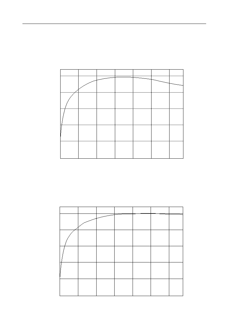
° Semiconductor
MSM7662
55/62
PEDL7662-02
Filter Characteristics
0
≠20
≠40
≠60
≠80
≠100
0
1
2
3
Frequency [MHz]
Band Pass Filter (NTSC ITU-RBT.601)
Level [dB]
4
5
6
0
≠20
≠40
≠60
≠80
≠100
0
1
2
3
Frequency [MHz]
Band Pass Filter (PAL ITU-RBT.601)
Level [dB]
4
5
6
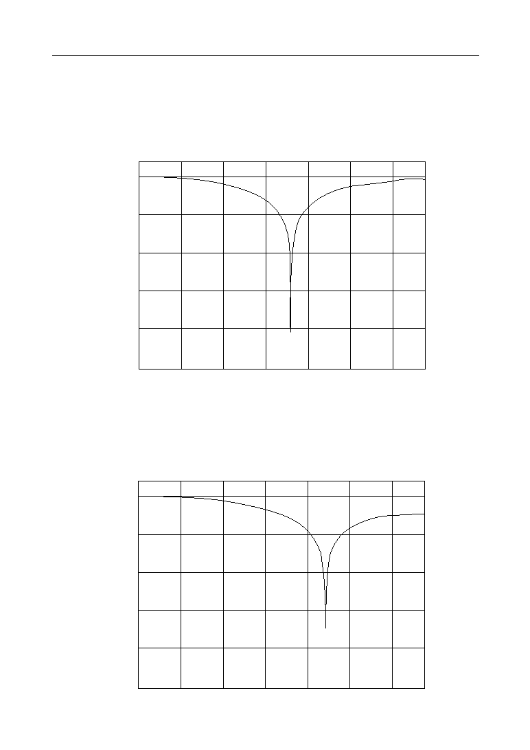
° Semiconductor
MSM7662
56/62
PEDL7662-02
0
≠20
≠40
≠60
≠80
≠100
0
1
2
3
Frequency [MHz]
Trap Filter (NTSC ITU-RBT.601)
Level [dB]
4
5
6
0
≠20
≠40
≠60
≠80
≠100
0
1
2
3
Frequency [MHz]
Trap Filter (PAL ITU-RBT.601)
Level [dB]
4
5
6
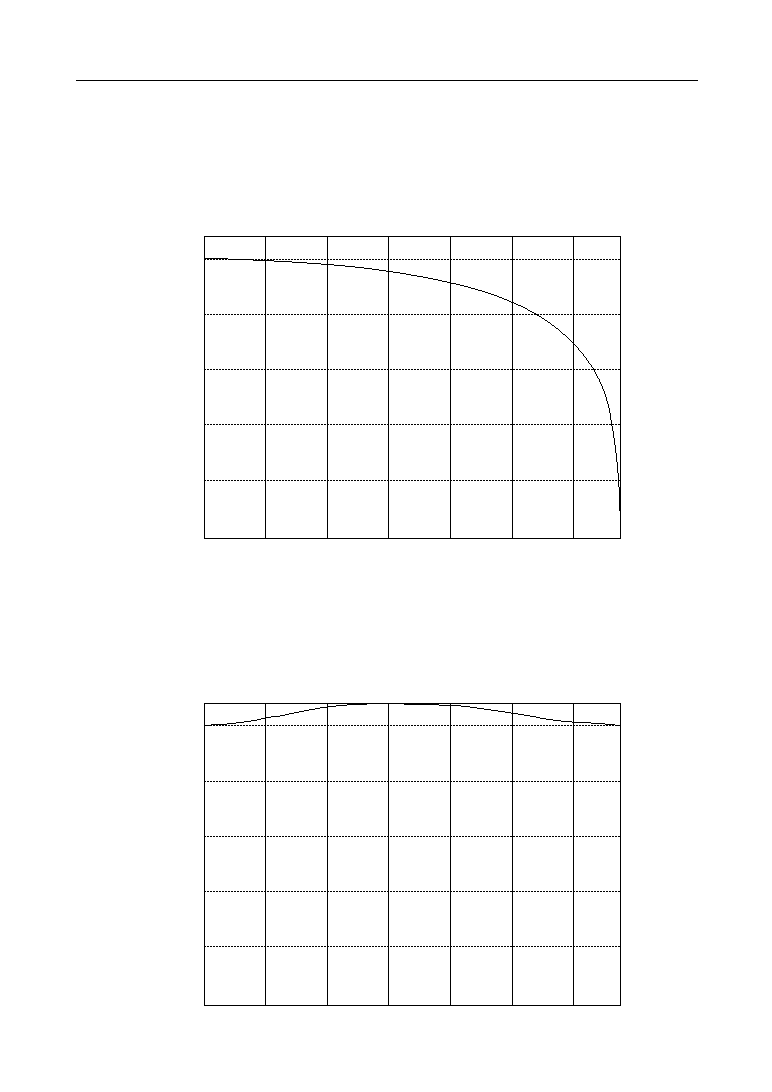
° Semiconductor
MSM7662
57/62
PEDL7662-02
0
≠20
≠40
≠60
≠80
≠100
0
1
2
3
Frequency [MHz]
Pre Filter
Level [dB]
4
5
6
0
≠20
≠40
≠60
≠80
≠100
0
1
2
3
Frequency [MHz]
Sharp Filter
Level [dB]
4
5
6

° Semiconductor
MSM7662
58/62
PEDL7662-02
0
≠20
≠40
≠60
≠80
≠100
0
2
4
6
Frequency [MHz]
Level [dB]
8
10
12
Decimation Filter
° Semiconductor
MSM7662
59/62
PEDL7662-02
BASIC APPLICATION CIRCUIT EXAMPLES
1) Application Circuit for FIFO-1 and FIFO-2 Modes
4
MSM7662
Video LSI
OSC
I
2
C
Controller
1
mF
2
1
mF
Video in
(C input)
SDA SCL RESET_L
AV
DD
DAV
DD
DV
DD
Y(7:0)
C(7:0)
B(7:0)
HVALID
VVALID
ODD
HSYNC_L
VSYNC_L
CLKX2O
CLKXO
CLKX2
MODE[3:0]
DGND
DAGND
AGND
10
mF
10
mF
1
mF
10
mF
10
mF
1
mF
10 k
W
Video in
(Composite
Y input)
4.7 k
W
4.7 k
W
3.3 V or 5 V
1000 pF
47
mF
1000 pF
47
mF
1000 pF
47
mF
VIN(1:4)
VRT1
AMPOUT
ADIN1
CLPOUT1
VRCL1
VRB1
VIN(5:6)
VRT2
AMPOUT2
ADIN2
CLPOUT2
VRB2
75
W
75
W
75
W
LPF
LPF
75
W
100
W
AMPOUT
LPF
ADIN
250 pF
∑ Connect the M7662 decoder and a video LSI device according to the output interface (ITU-
RBT.656, 8-bit [YCbCr], 16-bit [YCbCr], RGB).
∑ Video input can be four composite inputs or two S-Video inputs.
∑ Connect unused video input pins to AGND. If a composite signal is input, the C input side
(video amp, A/D converter, etc.) will be in the OFF operation state.
∑ If the input is limited by the composite signal, connect VIN (5:6), VRT2, VRB2, AMPOUT2,
ADIN2, and CLPOUT2 pins to AGND. Externally attached components such as capacitors
may be removed.
∑ Set the MODE[3:0] pins to the prescribed setting.
∑ Supply power and GND for analog, A/D, and digital circuits on the circuit board should be
separated at the power source wherever possible. Power and GND lines for analog and A/D
circuits must be wide and low impedance.
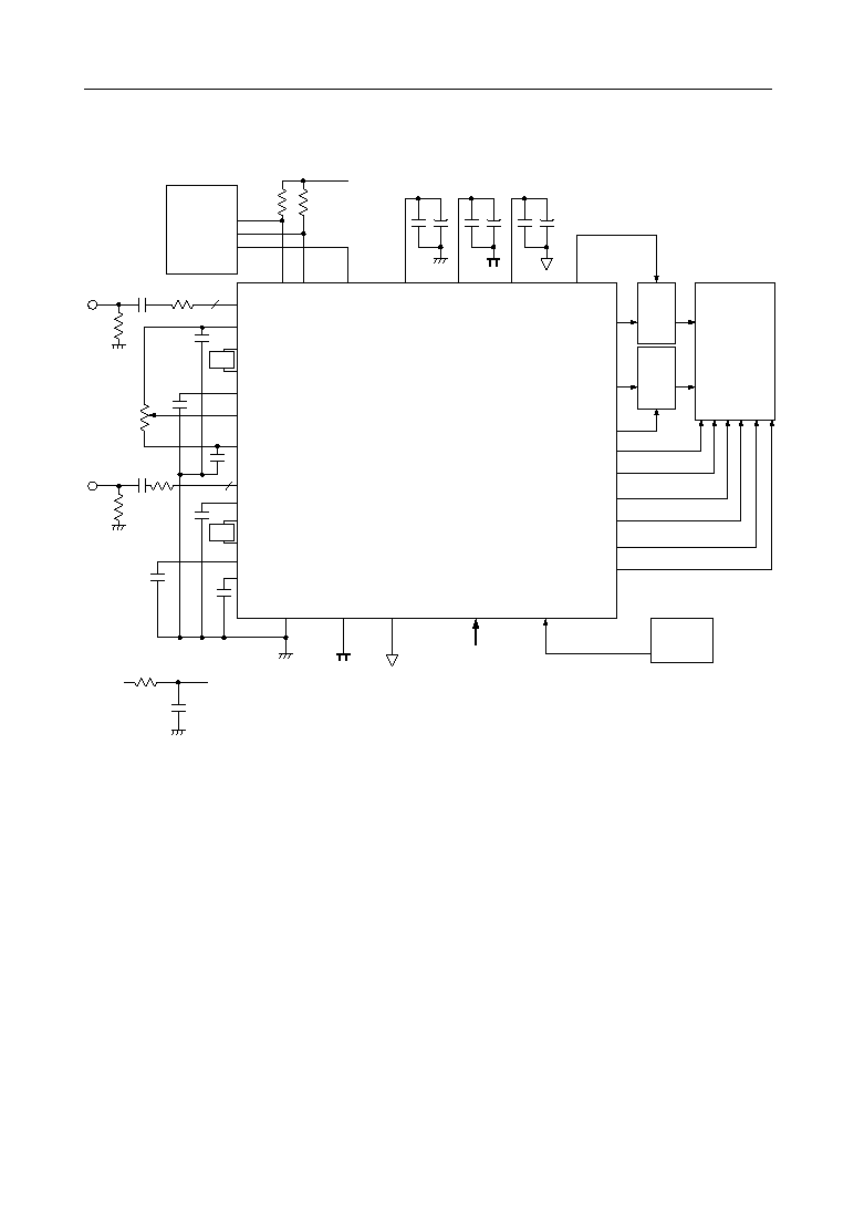
° Semiconductor
MSM7662
60/62
PEDL7662-02
2) Application Circuit for FM-1 and FM-2 Modes
∑ Select either 16-bit [YCbCr] or RGB output as the output interface.
∑ Number of field memories utilized
16-bit [YCbCr]: Use 2 field memories.
RGB: Use 3 field memories.
∑ Video input can be four composite inputs or two S-Video inputs.
∑ Connect unused video input pins to AGND. If a composite signal is input, the C input side
(video amp, A/D converter, etc.) will be in the OFF operation state.
∑ If the input is limited by the composite signal, connect VIN (5:6), VRT2, VRB2, AMPOUT2,
ADIN2, and CLPOUT2 pins to AGND. Externally attached components such as capacitors
may be removed.
∑ Set the MODE[3:0] pins to the prescribed setting.
∑ For the FM-1 mode setting, externally generate and supply control signals for the field
memory.
∑ For the FM-2 mode setting, memory control signals from M[7:4] can be supplied to the field
memory.
∑ For the FM-2 mode setting, the output timing for HSYNC_L, VSYNC_L, ODD, VVALID, and
HVALID becomes the memory read timing. Data output from memory is aligned with the
various sync signal timings. (See page 30 and page 31)
∑ Supply power and GND for analog, A/D, and digital circuits on the circuit board should be
separated at the power source wherever possible. Power and GND lines for analog and A/D
circuits must be wide and low impedance.
MSM7662
Video LSI
OSC
I
2
C
Controller
Video in
(C input)
SDA SCL RESET_L
AV
DD
DAV
DD
DV
DD
Y(7:0)
C(7:0)
B(7:0)
HVALID
VVALID
ODD
HSYNC_L
VSYNC_L
CLKX2O
CLKX2
MODE[3:0]
DGND
DAGND
AGND
10
mF
10
mF
1
mF
10
mF
1
mF
10 k
W
Video in
(Composite
Y input)
4.7 k
W
4.7 k
W
3.3 V or 5 V
1000 pF
47
mF
1000 pF
47
mF
1000 pF
47
mF
VIN(1:4)
VRT1
AMPOUT
ADIN1
CLPOUT1
VRCL1
VRB1
VIN(5:6)
VRT2
AMPOUT2
ADIN2
CLPOUT2
VRB2
Memory
control signal
M[7:4]
Field
mem-
ory
Field
mem-
ory
CLKXO
75
W
75
W
4
1
mF
2
1
mF
10
mF
75
W
LPF
75
W
100
W
AMPOUT
LPF
ADIN
250 pF
LPF
° Semiconductor
MSM7662
61/62
PEDL7662-02
(Unit : mm)
PACKAGE DIMENSIONS
Notes for Mounting the Surface Mount Type Package
The SOP, QFP, TSOP, TQFP, LQFP, SOJ, QFJ (PLCC), SHP, and BGA are surface mount type
packages, which are very susceptible to heat in reflow mounting and humidity absorbed in
storage. Therefore, before you perform reflow mounting, contact Oki's responsible sales person
on the product name, package name, pin number, package code and desired mounting conditions
(reflow method, temperature and times).
TQFP100-P-1414-0.50-K
Package material
Lead frame material
Pin treatment
Solder plate thickness
Package weight (g)
Epoxy resin
42 alloy
Solder plating
5
mm or more
0.55 TYP.
Mirror finish

° Semiconductor
MSM7662
62/62
PEDL7662-02
NOTICE
1.
The information contained herein can change without notice owing to product and/or
technical improvements. Before using the product, please make sure that the information
being referred to is up-to-date.
2.
The outline of action and examples for application circuits described herein have been
chosen as an explanation for the standard action and performance of the product. When
planning to use the product, please ensure that the external conditions are reflected in the
actual circuit, assembly, and program designs.
3.
When designing your product, please use our product below the specified maximum
ratings and within the specified operating ranges including, but not limited to, operating
voltage, power dissipation, and operating temperature.
4.
Oki assumes no responsibility or liability whatsoever for any failure or unusual or
unexpected operation resulting from misuse, neglect, improper installation, repair, alteration
or accident, improper handling, or unusual physical or electrical stress including, but not
limited to, exposure to parameters beyond the specified maximum ratings or operation
outside the specified operating range.
5.
Neither indemnity against nor license of a third party's industrial and intellectual property
right, etc. is granted by us in connection with the use of the product and/or the information
and drawings contained herein. No responsibility is assumed by us for any infringement
of a third party's right which may result from the use thereof.
6.
The products listed in this document are intended for use in general electronics equipment
for commercial applications (e.g., office automation, communication equipment,
measurement equipment, consumer electronics, etc.). These products are not authorized
for use in any system or application that requires special or enhanced quality and reliability
characteristics nor in any system or application where the failure of such system or
application may result in the loss or damage of property, or death or injury to humans.
Such applications include, but are not limited to, traffic and automotive equipment, safety
devices, aerospace equipment, nuclear power control, medical equipment, and life-support
systems.
7.
Certain products in this document may need government approval before they can be
exported to particular countries. The purchaser assumes the responsibility of determining
the legality of export of these products and will take appropriate and necessary steps at their
own expense for these.
8.
No part of the contents contained herein may be reprinted or reproduced without our prior
permission.
Copyright 1999 Oki Electric Industry Co., Ltd.
Printed in Japan