 | –≠–ª–µ–∫—Ç—Ä–æ–Ω–Ω—ã–π –∫–æ–º–ø–æ–Ω–µ–Ω—Ç: MSM7716 | –°–∫–∞—á–∞—Ç—å:  PDF PDF  ZIP ZIP |

° Semiconductor
MSM7716
1/22
° Semiconductor
MSM7716
Single Rail Linear CODEC
GENERAL DESCRIPTION
The MSM7716 is a single-channel CODEC CMOS IC for voice signals that contains filters for
linear A/D and D/A conversion.
Designed especially for a single-power supply and low-power applications, the device is
optimized for applications for the analog interfaces of audio signal processing DSPs and digital
wireless systems.
The analog output signal can directly drive a ceramic type handset receiver. In addition, levels
for analog outputs can be set by external control.
FEATURES
∑ Single power supply
: +2.7 V to +3.6 V
∑ Low power consumption
Operating mode
: 24 mW Typ.
Power down mode
: 0.05 mW Typ.
∑ Digital signal input/output interface
: 14-bit serial code in 2's complement format
∑ Sampling frequency(fs)
: 4 to 16 kHz
∑ Transmission clock frequency
: fs • 14 min., 2048 kHz max.
∑ Filter characteristics
: when fs = 8 kHz, complies with ITU-T Recommen-
dation G. 714
∑ Built-in PLL eliminates a master clock
∑ Two input circuits in transmit section
∑ Two output circuits in receive section
∑ Transmit gain adjustable using an external resistor
∑ Receive gain adjustable by external control 8 steps, 4 dB/step
∑ Transmit mic-amp is eliminated by the gain setting of a maximum of 36 dB.
∑ Analog outputs can drive a load of a minimum of 1 kW ; an amplitude of a maximum of 4.0 V
PP
with push-pull driving.
∑ Built-in reference voltage supply
∑ Package options:
32-pin plastic TSOP (TSOPI32-P-814-0.50-1K) (Product name : MSM7716TS-K)
30-pin plastic SSOP (SSOP30-P-56-0.65-K)
(Product name : MSM7716GS-K)
E2U0043-28-82
This version: Aug. 1998
Previous version: Nov. 1996
° Semiconductor
MSM7716
2/22
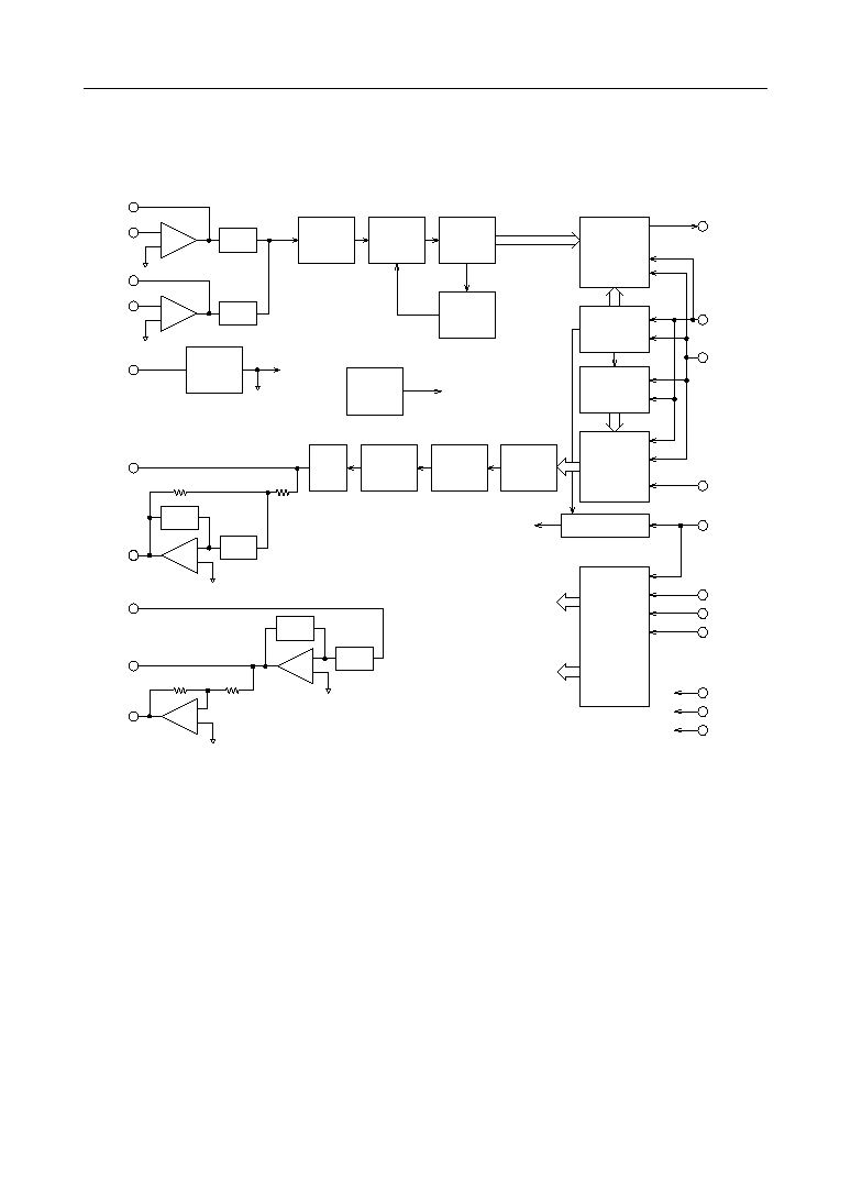
BLOCK DIAGRAM
MAIN
≠
+
MAO
SW 1
PBIN
≠
+
PBO
SW 2
RC
LPF
8th
BPF
14 BIT
ADCONV
TCONT
PLL
RTIM
RCONT
PWD logic
PCMOUT
5th
LPF
14 BIT
DACONV
RC
LPF
VOL
AUTO
ZERO
VR
GEN
SG
GEN
SGC
SG
≠
+
SW 4
SW 4
VFO
AUXO
≠
+
AOUT+
≠
+
SW 3
SW 3
AOUT≠
PWI
CONT
Logic
PWD
SW
CONT
VOL
CONT
SYNC
BCLK
PCMIN
PDN
DEN
CDIN
DCLK
V
DD
AG
DG
° Semiconductor
MSM7716
3/22
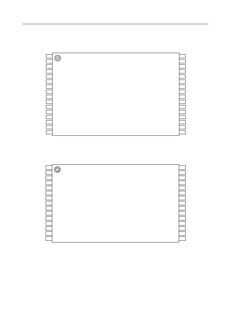
PIN CONFIGURATION (TOP VIEW)
1
2
3
4
5
6
7
8
9
10
11
12
13
14
15
16
17
18
19
20
21
22
23
24
25
26
27
28
29
30
31
32
MAIN
MAO
PBO
PBIN
SGC
AG
AUXO
AOUT+
AOUT≠
PWI
VFO
V
DD
DCLK
CDIN
DEN
DG
PCMIN
PCMOUT
BCLK
SYNC
PDN
NC : No connect pin
NC
NC
NC
NC
NC
NC
NC
NC
NC
NC
NC
32-Pin Plastic TSOP
1
2
3
4
5
6
7
8
9
10
11
12
13
14
15
16
17
18
19
20
21
22
23
24
25
26
27
28
29
30
AG
AUXO
PWI
VFO
NC
NC
V
DD
DCLK
NC
DG
PCMIN
SYNC
PDN
NC
NC
MAIN
MAO
PBIN
SGC
NC : No connect pin
AOUT+
AOUT≠
NC
CDIN
DEN
NC
PBO
BCLK
NC
PCMOUT
NC
30-Pin Plastic SSOP
° Semiconductor
MSM7716
4/22
PIN AND FUNCTIONAL DESCRIPTIONS
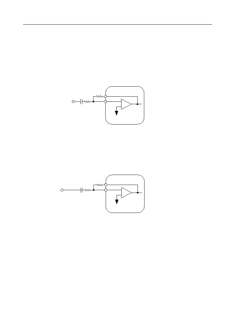
MAIN, MAO
Transmit microphone input and the level adjustment.
MAIN is connected to the noninverting input of the op-amp, and MAO is connected to the output
of the op-amp. The level adjustment should be configured as shown below.
During power saving and power down modes, the MAO output is in high impedance state.
≠
+
MAIN
C1
Microphone input
R1 : variable
R2 > 20 kW
C1 > 1/(2 • 3.14 • 30 • R1) (F)
Gain = R2/R1 < 63
R2
MAO
R1
SG
PBIN, PBO
Transmit handset input and the level adjustment.
PBIN is connected to the noninverting input of the op-amp, and PBO is connected to the output
of the op-amp. The level adjustment should be configured as shown below.
During power saving and power down, the PBO output is in high impedance state.
V
DD
Power supply pin for +2.7 to 3.6 V (Typically 3.0 V).
AG
Analog signal ground.
DG
Ground pin for the digital signal circuits.
This ground is separated from the analog signal ground in this device. The DG pin must be
connected to the AG pin on the printed circuit board.
≠
+
PBIN
C2
R3 : variable
R4 > 20 kW
C2 > 1/(2 • 3.14 • 30 • R3) (F)
Gain = R4/R3 < 63
R4
PBO
R3
SG
Handset
microphone input

° Semiconductor
MSM7716
5/22
VFO
Receive filter output.
The output signal has an amplitude of 2.0 V
PP
above and below the signal ground voltage when
the digital signal of +3 dBm0 is input to PCMIN. VFO can drive a load of 20 kW or more.
This output can be externally controlled in the level range of 0 to ≠28 dB in 4 dB increments.
During power saving or power down, VFO output is at the voltage level (V
DD
/2) of SG with a
high impedance state.
PWI, AOUT+, AOUT≠
PWI is connected to the inverting input of the receive driver.
The receive driver output is connected to the AOUT≠ pin. Thus, a receive level can be adjusted
with the pins PWI, AOUT≠, and VFO described above.
The output of AOUT+ is inverted with respect to the output of AOUT≠ with a gain of 1.
The output signal amplitudes are a maximum of 2.0 V
PP
.
These outputs, above and below the signal ground voltage (V
DD
/2), can drive a load of a
minimum of 1 kW with push-pull driving (a load connected between AOUT+ and AOUT≠).
The output amplitudes are 4 V
PP
maximum during push-pull driving. These outputs can be
mute controlled externally. These outputs are operational during power saving and output the
SG voltage (V
DD
/2) in the high impedance state.
AUXO
Auxiliary receive filter output.
The output signal is inverted with respect to the VFO output with a gain of 1. The output signal
swings above and below the SG voltage (V
DD
/2), and can drive a minimum load of 0.5 kW with
respect to the SG voltage.
The output can be mute controlled externally.
During power saving and power down, AUXO outputs the SG voltage (V
DD
/2) in the high
impedance state.
BCLK
Shift clock signal input for PCMIN and PCMOUT.
The frequency is equal to the data rate. Setting this signal to logic "1" or "0" drives both transmit
and receive circuits to the power-saving state.

° Semiconductor
MSM7716
6/22
SYNC
Synchronizing signal input.
In the transmit section, the PCM output signal from the PCMOUT pin is output synchronously
with this synchronizing signal. This synchronizing signal triggers the PLL and synchronizes all
timing signals of the transmit section.
In the receive section, 14 bits required are selected from serial input of PCM signals on the PCMIN
pin by the synchronizing signal.
Signals in the receive section are synchronized by this synchronizing signal. This signal must be
synchronized in phase with the BCLK.
When this signal frequency is 8 kHz, the transmit and receive section have the frequency
characteristics specified by ITU-T G. 714. The frequency characteristics for 8 kHz are specified in
this data sheet.
For different frequencies of the SYNC signal, the frequency values in this data sheet should be
translated according to the following equation:
Frequency values described in the data sheet • the SYNC frequency values to be actually used
8 kHz
Setting this signal to logic "1" or "0" drives the device to power-saving state.
PCMIN
PCM signal input.
A serial PCM signal input to this pin is converted to an analog signal synchronously with the
SYNC signal and BCLK signal.
The data rate of the PCM signal is equal to the frequency of the BCLK signal.
The PCM signal is shifted at a falling edge of the BCLK signal. The PCM signal is latched into the
internal register when shifted by 14 bits.
The top of the data (MSD) is identified at the rising edge of SYNC.
The input signal should be input in the 14-bit 2's complement format.
The MSD bit represents the polarity of the signal with respect to the signal ground.
° Semiconductor
MSM7716
7/22
PCMOUT
PCM signal output.
The PCM output signal is output from MSD in sequential order, synchronously with the rising
edge of the BCLK signal.
MSD may be output at the rising edge of the SYNC signal, depending on the timing between
BCLK and SYNC.
This pin is in high impedance state except during 14-bit PCM output. It is also high impedance
during power saving or power down mode.
A pull-up resistor must be connected to this pin, because its output is configured as an open
drain.
The output coding format is in 14-bit 2's complement.
The MSD represents a polarity of the signal with respect to the signal ground.
Table 1
Input/Output Level
+Full scale
+1
0
≠Full scale
PCMIN/PCMOUT
MSD
0 1 1 1 1 1 1 1 1 1 1 1 1 1
0 0 0 0 0 0 0 0 0 0 0 0 0 1
0 0 0 0 0 0 0 0 0 0 0 0 0 0
1 0 0 0 0 0 0 0 0 0 0 0 0 0
≠1
1 1 1 1 1 1 1 1 1 1 1 1 1 1
PDN
Power down control signal input.
A digital "L" level drives both transmit and receive circuits to a power down state.
The control registers are set to the initial state.
SGC
Connection of a bypass capacitor for generating the signal ground voltage level.
Connect a 0.1 mF capacitor with excellent high frequency characteristics between the AG pin and
the SGC pin.
° Semiconductor
MSM7716
8/22
DEN, DCLK, CDIN
Serial control ports for the microcontroller interface.
Writing data to the 8-bit control register enables control of the receive output level and the signal
path.
DEN is the "Enable" signal pin, DCLK is the data shift clock input pin, and CDIN is the control
data input pin.
When powered down (PDN = 0), the initial values are set as shown in Tables 2, 3, and 4. The initial
values are held unless the control data is written after power-down release.
The control data is shifted at the rising edge of the DCLK signal and latched into the internal
control register at the rising edge of the DEN signal.
When the microcontroller interface is not used, these pins should be connected to DG.
The bit map of the 8-bit control register is shown below.
B7
SW1
B6
SW2
B5
SW3
B4
SW4
B3
--
B2
VOL1
B1
VOL2
B0
VOL3
° Semiconductor
MSM7716
9/22
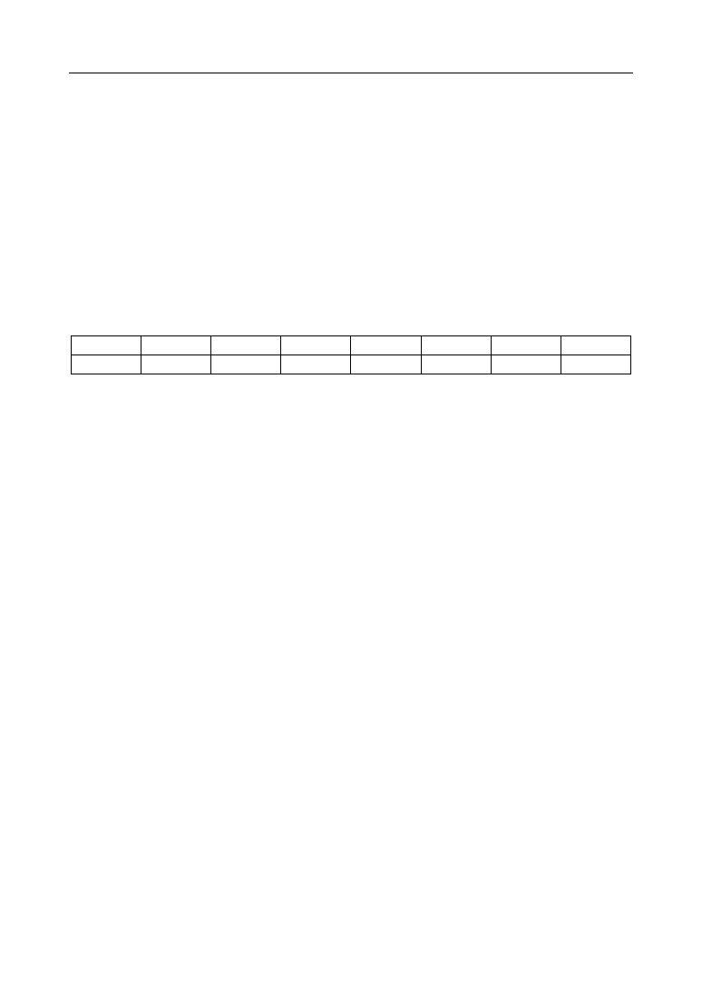
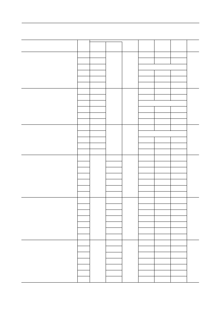
ABSOLUTE MAXIMUM RATINGS
Parameter
Power Supply Voltage
Analog Input Voltage
Digital Input Voltage
Storage Temperature
Symbol
V
DD
V
AIN
V
DIN
T
STG
Condition
AG = DG = 0 V
AG = DG = 0 V
AG = DG = 0 V
--
Rating
≠0.3 to +7.0
≠0.3 to V
DD
+ 0.3
≠0.3 to V
DD
+ 0.3
≠55 to +150
Unit
V
V
V
∞C
RECOMMENDED OPERATING CONDITIONS
Parameter
Power Supply Voltage
Operating Temperature
Analog Input Voltage
High Level Input Voltage
Low Level Input Voltage
Clock Frequency
Sync Pulse Frequency
Clock Duty Ratio
Digital Input Rise Time
Digital Input Fall Time
Sync Pulse Setting Time
High Level Sync Pulse Width *1
Low Level Sync Pulse Width *1
PCMIN Setup Time
PCMIN Hold Time
Digital Output Load
DCLK Pulse Width
DEN Setting Time 1
DEN Setting Time 2
CDIN Setup Time
CDIN Hold Time
Analog Input Allowable DC Offset
Allowable Jitter Width
Symbol
V
DD
Ta
V
AIN
V
IH
V
IL
F
C
F
S
D
C
t
Ir
t
If
t
XS
, t
RS
t
WSH
t
DS
t
DH
R
DL
t
WCL
t
CDL
t
CDH
t
CDS
t
CDH
V
off
--
t
SX
, t
SR
C
DL
t
WCH
t
DCL
t
DCH
Condition
--
--
Gain = 1
SYNC, BCLK, PCMIN, PDN,
DEN, DCLK, CDIN
BCLK
SYNC
BCLK
SYNC, BCLK, PCMIN, PDN,
DEN, DCLK, CDIN
BCLK∆SYNC, See Fig.1
SYNC, See Fig.1
Refer to Fig.1
Refer to Fig.1
Pull-up resistor
DCLK Low width, See Fig.2
DCLK∆DEN, See Fig.2
DCLK∆DEN, See Fig.2
See Fig.2
See Fig.2
Transmit gain stage, Gain = 0 dB
SYNC, BCLK
SYNC∆BCLK, See Fig.1
--
DCLK High width, See Fig.2
DEN∆DCLK, See Fig.2
DEN∆DCLK, See Fig.2
Transmit gain stage, Gain = 20 dB
Min.
2.7
≠30
--
0.45 •
V
DD
0
14 • Fs
4.0
40
--
--
100
1 BCLK
100
100
0.5
50
50
50
50
50
≠100
--
100
--
50
50
50
≠10
Typ.
3.0
+25
--
--
--
--
8.0
50
--
--
--
--
--
--
--
--
--
--
--
--
--
--
--
--
--
--
--
--
Max.
3.6
+85
1.4
V
DD
0.16 •
V
DD
128 • Fs
16
60
50
50
--
--
--
--
--
--
--
--
--
--
+100
1000
--
100
--
--
--
+10
Unit
V
∞C
V
PP
V
V
kHz
kHz
%
ns
ns
ns
--
ns
ns
kW
ns
ns
ns
ns
mV
ns
ns
pF
mV
t
WSL
SYNC, See Fig.1
1 BCLK
--
--
--
*1 For example, the minimum pulse width of SYNC is 488 ns when the frequency of BCLK is
2048 kHz.
° Semiconductor
MSM7716
10/22
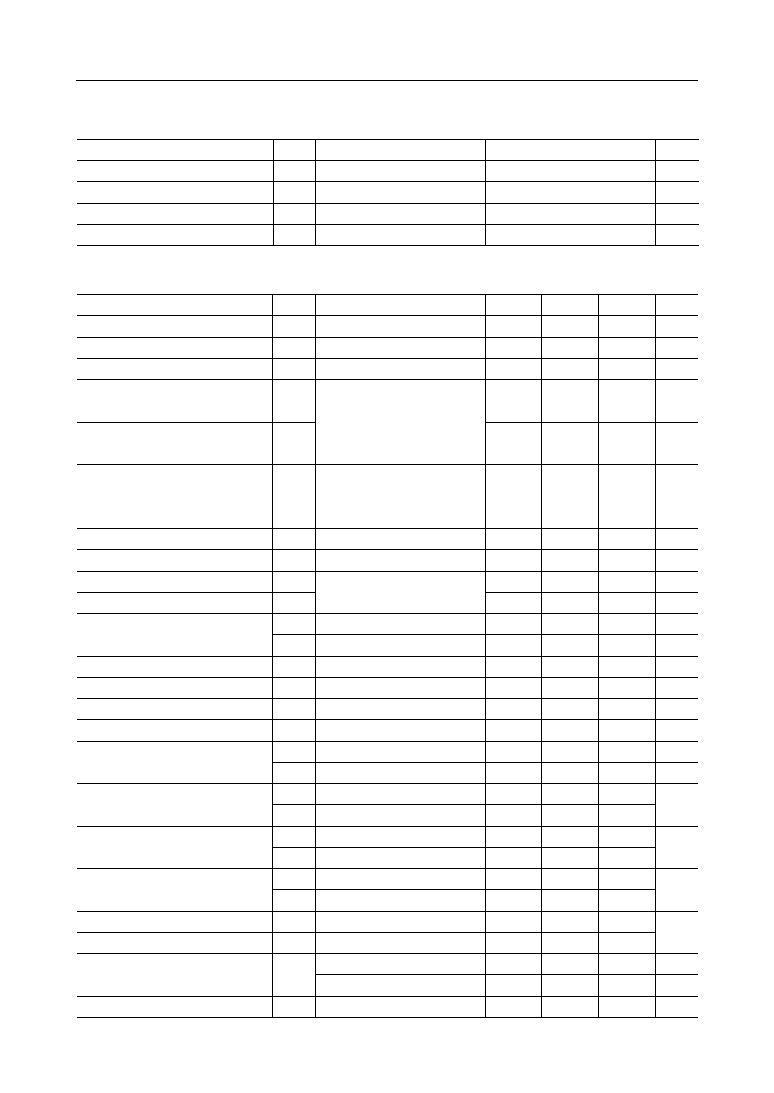
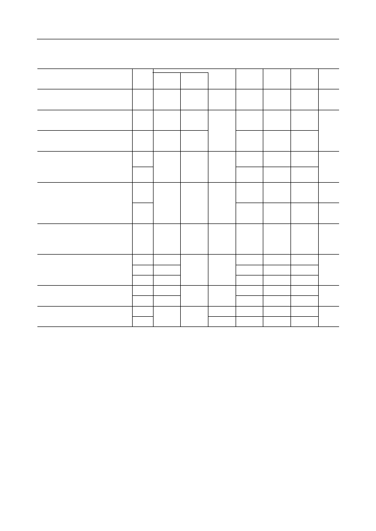
RECOMMENDED OPERATING CONDITIONS
(Continued)
ELECTRICAL CHARACTERISTICS
DC and Digital Interface Characteristics
Parameter
Digital Output Delay Time
Symbol
t
SD
t
XD1
t
XD2
t
XD3
Min.
20
20
20
20
Typ.
--
--
--
--
Max.
100
100
100
100
Unit
ns
Condition
C
L
= 50 pF + 1 LSTTL
Pull-up resistor = 500 W
Parameter
Power Supply Current
High Level Input Voltage
Low Level Input Voltage
High Level Input Leakage Current
Low Level Input Leakage Current
Digital Output Low Voltage
Digital Output Leakage Current
Input Capacitance
Symbol
I
DD1
I
DD2
I
DD3
V
IH
V
IL
I
IH
I
IL
V
OL
I
O
Condition
Operating mode,
No signal
Power-saving mode, PDN = 1,
SYNC, BCLK ∆ OFF
Power-down mode, PDN = 0
--
--
PCMOUT pull-up resistor = 500 W
--
Min.
--
--
--
--
0.45 •
V
DD
0.0
--
--
0.0
--
Typ.
10.0
8.0
6.0
0.01
--
--
--
--
0.2
--
Max.
17.0
13.0
11.0
0.05
V
DD
0.16 •
V
DD
2.0
0.5
0.4
10
Unit
mA
mA
mA
V
V
m
A
m
A
V
m
A
V
DD
= 3.6 V
V
DD
= 3.0 V
C
IN
--
--
5
--
pF
(Fs = 8 kHz, V
DD
= 2.7 V to 3.6 V, Ta = ≠30∞C to +85∞C)
mA
SYNC, BCLK, PCMIN, DEN,
CDIN, DCLK, PDN
° Semiconductor
MSM7716
11/22
Transmit Analog Interface Characteristics
Receive Analog Interface Characteristics
Input Resistance
Output Load Resistance
Output Load Capacitance
Output Amplitude
Offset Voltage
R
INX
R
LGX
C
LGX
V
OGX
V
OSGX
MAIN, PBIN
Gain = 1
10
20
--
≠0.7
≠20
--
--
--
--
--
--
--
30
+0.7
+20
MW
kW
pF
V
mV
MAO, PBO with respect to SG
Parameter
Symbol
Condition
Min.
Typ.
Max.
Unit
(Fs = 8 kHz, V
DD
= 2.7 V to 3.6 V, Ta = ≠30∞C to +85∞C)
Output Resistance
Output Load Resistance
Output Load Capacitance
R
OAO
R
LVO
R
LAO
C
LAO
AUXO, AOUT+, AOUT-
--
20
0.5
--
--
--
--
--
10
--
--
50
W
kW
kW
pF
VFO with respect to SG
Output Amplitude
Offset Voltage
V
OAO
V
OSA
≠1.0
≠100
--
--
+1.0
+100
V
mV
AUXO, AOUT+, AOUT≠ (each)
with respect to SG
Output open
AUXO, AOUT+, AOUT≠, VFO
with respect to SG
AUXO, AOUT+, AOUT≠, VFO
with respect to SG
Parameter
Symbol
Condition
Min.
Typ.
Max.
Unit
(Fs = 8 kHz, V
DD
= 2.7 V to 3.6 V, Ta = ≠30∞C to +85∞C)
R
OVO
VFO
--
--
100
W
° Semiconductor
MSM7716
12/22
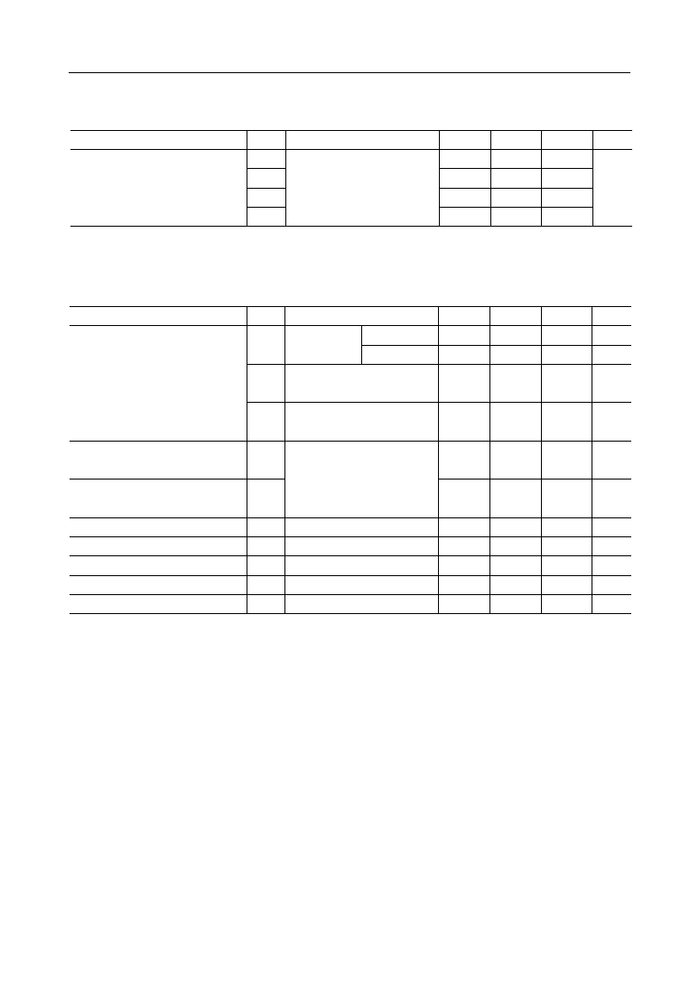
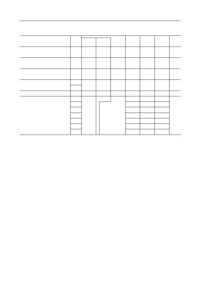
AC Characteristics
Condition
(Fs = 8 kHz, V
DD
= 2.7 V to 3.6 V, Ta = ≠30∞C to +85∞C)
Parameter
Symbol
Min.
Typ.
Max.
Unit
Transmit Frequency Response
(Expected Value)
Loss T1
Level
(dBm0)
60
20
--
--
Freq.
(Hz)
Loss T2
300
≠0.15
--
+0.2
Loss T3
1020
Reference
dB
0
Loss T4
2020
≠0.15
--
+0.2
Loss T5
3000
≠0.15
--
+0.2
Loss T6
3400
0
--
0.8
Receive Frequency Response
(Expected Value)
Loss R1
300
≠0.15
--
+0.2
Loss R2
1020
Reference
Loss R3
2020
≠0.15
--
+0.2
dB
0
Loss R4
3000
≠0.15
--
+0.2
Loss R5
3400
0.0
--
0.8
SD T1
58
--
--
3
SD T2
58
--
--
0
SD T3
58
--
--
≠10
Transmit Signal to Distortion Ratio
(Expected Value)
1020
dB
SD T4
48
--
--
≠20
*1
SD T5
38
--
--
≠30
SD R1
58
--
--
SD R2
58
--
--
SD R3
58
--
--
Receive Signal to Distortion Ratio
(Expected Value)
1020
dB
SD R4
48
--
--
*1
SD R5
38
--
--
3
0
≠10
≠20
≠30
SD T6
28
--
--
≠40
SD T7
18
--
--
≠50
SD R6
28
--
--
≠40
SD R7
18
--
--
≠50
Overall Frequency Response
Loss 1
60
20
--
--
Loss 2
300
≠0.2
--
+0.4
Loss 3
1020
Reference
dB
0
Loss 4
2020
≠0.2
--
+0.4
Loss 5
3000
≠0.2
--
+0.4
Loss 6
3400
0
--
1.6
SD 1
55.9
--
--
3
SD 2
55.9
--
--
0
SD 3
55.9
--
--
≠10
Overall Signal to Distortion Ratio
1020
dB
SD 4
45.9
--
--
≠20
*1
SD 5
35.9
--
--
≠30
SD 6
25.9
--
--
≠40
SD 7
15.9
--
--
≠50
Analog
to
Analog
Analog
to
Analog
*1
Psophometric filter is used.

° Semiconductor
MSM7716
13/22
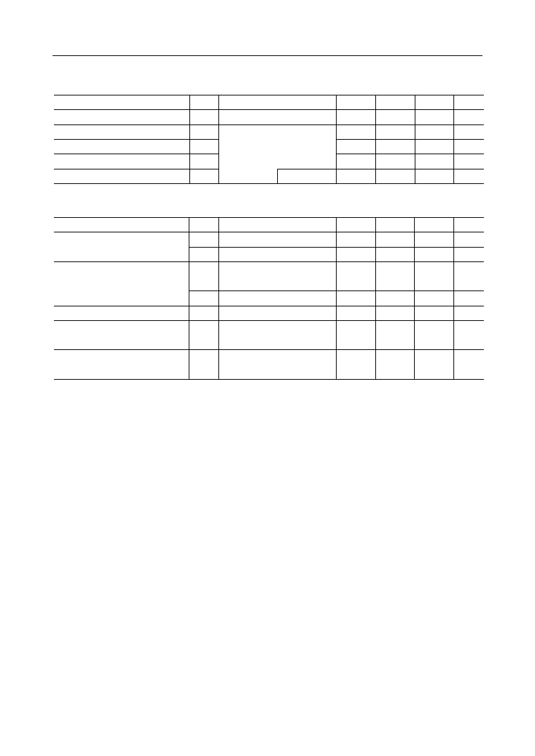
AC Characteristics (Continued)
Condition
(Fs = 8 kHz, V
DD
= 2.7 V to 3.6 V, Ta = ≠30∞C to +85∞C)
Parameter
Symbol
Min.
Typ.
Max.
Unit
Level
(dBm0)
Freq.
(Hz)
3
≠10
≠40
≠50
≠55
Transmit Gain Tracking
(Expected Value)
GT T1
≠0.3
+0.01
+0.3
GT T2
Reference
GT T3
1020
≠0.3
0.00
+0.3
dB
GT T4
≠0.6
≠0.03
+0.6
GT T5
≠1.2
+0.15
+1.2
Receive Gain Tracking
(Expected Value)
GT R1
≠0.3
≠0.06
+0.3
GT R2
Reference
GT R3
1020
≠0.3
≠0.02
+0.3
dB
GT R4
≠0.6
≠0.02
+0.6
GT R5
≠1.2
≠0.27
+1.2
3
≠10
≠40
≠50
≠55
3
≠10
≠40
≠50
≠55
Overall Gain Tracking
GT 1
≠0.4
+0.01
+0.4
GT 2
Reference
GT 3
1020
≠0.3
0.00
+0.8
dB
GT 4
≠1.3
≠0.03
+1.3
GT 5
≠1.6
≠0.15
+1.6
Analog
to
Analog
° Semiconductor
MSM7716
14/22
AC Characteristics (Continued)
Absolute Level (Initial Level)
Nidle T
--
--
≠76
≠74
dBmOp
Nidle R
--
≠76
AV T
0.338
0.350
0.362
AV R
0.483
0.500
0.518
Vrms
1020
Absolute Delay
AV Tt
≠0.2
--
+0.2
0
AV Rt
≠0.2
--
+0.2
t
D
1020
--
--
0.6
ms
0
A to A
BCLK
= 64 kHz
Transmit Group Delay
t
GD
T1
--
--
0.325
t
GD
T2
--
--
0.175
0
ms
*3
--
t
GD
T3
--
0.325
Receive Group Delay
--
0.00
0.125
ms
0
--
0.12
0.325
--
≠74
Transmit Idle Channel Noise
(Expected Value)
--
--
AIN: no signal
*1
dB
dB
V
DD
= 3.0 V
Ta = 25∞C
V
DD
= +2.7
to 3.6 V
Ta = ≠30
to 85∞C
Absolute Level
(Deviation of Temperature and Power)
*2
500
600 to 2600
2800
Crosstalk Attenuation
CR T
75
85
--
CR R
80
1020
dB
0
TRANS ∆ RECV
RECV ∆ TRANS
t
GD
R1
t
GD
R2
2800
*3
70
--
Condition
Parameter
Symbol
Min.
Typ.
Max.
Unit
Level
(dBm0)
Freq.
(Hz)
(Fs = 8 kHz, V
DD
= 2.7 V to 3.6 V, Ta = ≠30∞C to +85∞C)
Receive Idle Channel Noise
(Expected Value)
500 to 2600
Nidle A
--
--
≠70
≠66
dBmOp
Overall Idle Channel Noise
--
AIN: no signal
*1
*1
Psophometric filter is used.
*2
AVT is defined at MAO and PBO-PCMOUT.
AVR is defined at PCMIN-VFO.
VOL = 0 dB
*3
Minimum value of the group delay distortion
° Semiconductor
MSM7716
15/22
AC Characteristics (Continued)
*1
Measured inband.
DIS
4.6 kHz to
30
32
--
dB
VOL Gain Setting Value
G
V5
≠17
≠16
≠15
G
V6
≠21
≠20
≠19
G
V7
≠25
≠24
≠23
G
V8
≠29
≠28
≠27
dB
Discrimination
0
0 to
4000 Hz
S
300 to
--
≠37.5
≠35
dBm0
Out-of-band Spurious
0
4.6 kHz to
IMD
fa = 470
--
≠52
≠40
dBm0
Intermodulation Distortion
≠4
2fa ≠ fb
PSR T
0 to
--
30
--
dB
Power Supply Noise Rejection Ratio
50 mV
PP
*1
PSR R
72 kHz
3400
fb = 320
50 kHz
100 kHz
Condition
Parameter
Symbol
Min.
Typ.
Max.
Unit
Level
(dBm0)
Freq.
(Hz)
(Fs = 8 kHz, V
DD
= 2.7 V to 3.6 V, Ta = ≠30∞C to +85∞C)
G
V4
≠13
≠12
≠11
G
V3
≠9
≠8
≠7
G
V2
≠5
≠4
≠3
G
AUX
≠1.0
0
+1.0
Auxiliary Output Gain
1020
0
VFO to AUXO
dB
1020
0
Set at ≠ 4 dB
≠8 dB
≠12 dB
≠16 dB
≠20 dB
≠24 dB
≠28 dB
Referenced
to 0 dB
setting
° Semiconductor
MSM7716
16/22
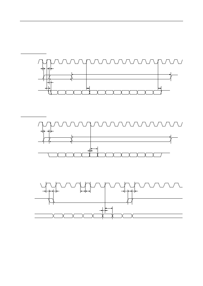
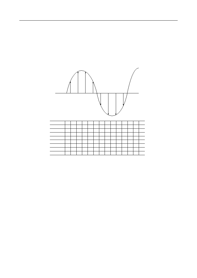
TIMING DIAGRAM
PCM Data Output Timing
BCLK
1
2
3
4
5
6
7
8
9
10
SYNC
PCMOUT
D9
D10 D11 D12 D13 D14
MSD
t
XS
t
SX
t
WSH
t
SD
t
XD1
t
XD2
t
XD3
BCLK
SYNC
PCMIN
Transmit Timing
Receive Timing
,
11
When t
XS
£
1/2 ∑ Fc, the Delay of the MSD bit is defined as t
XD1
.
When t
SX
<
1/2 ∑ Fc, the Delay of the MSD bit is defined as t
SD
.
12
13
14
15
16
17
D2
D3
D4
D5
D6
D7
D8
1
2
3
4
5
6
7
8
9
10
D9
D10 D11 D12 D13 D14
MSD
t
RS
t
SR
t
WSH
t
DS
,
11
12
13
14
15
16
17
D2
D3
D4
D5
D6
D7
D8
t
DH
t
WSL
t
WSL
Figure 1 Basic Timing Diagram
MCU Interface Timing
t
CDL
t
DCL
t
CDH
t
DCH
t
WCH
t
WCL
DCLK
1
2
3
4
5
6
7
8
9
10
11
12
13
DEN
,
,
B3
B4
B5
B6
B7
B2
B1
B0
CDIN
t
CDH
t
CDS
Figure 2 MCU Interface Timing Diagram
° Semiconductor
MSM7716
17/22
FUNCTIONAL DESCRIPTION
Control Data Description
SW1, SW2 - -
Control bits for the transmit speech path switch.
The AD converter input is selected according to the bit data shown in Table 2.
Table 2
State
SW2
SW1
AD Converter Input
Remarks
T1
0
0
No signal (muting state)
--
T2
0
1
Input signal to MAIN
At initial setting
T3
1
0
Input signal to PBIN
--
T4
1
1
Addition signal of both MAIN and PBIN
The gain of each input drops about 6 dB
SW3, SW4 - -
Control bits for the receive speech path switch.
The control should be performed according to Table 3.
Table 3
State
SW3
AOUT+, AOUT≠ Output
AUXO Output
R1
0
SG
SG
R2
1
PWI
SG
R3
0
SG
DA
R4
1
PWI
DA
Remarks
--
At initial setting
--
--
DA: DA converter output. SG: signal ground voltage.
SW4
0
0
1
1
VOL1, VOL2, VOL3 - - -
Control bits for the receive signal output level.
By controlling these bits, the output levels of VFO and AUXO can be
controlled according to Table 4.
Table 4
VOL1
VOL2
VOL3
Receive Signal Gain
Remarks
0
0
0
0 dB
At initial setting
0
0
1
≠4 dB
--
0
1
0
≠8 dB
--
0
1
1
≠12 dB
--
1
0
0
≠16 dB
--
1
0
1
≠20 dB
--
1
1
0
≠24 dB
--
1
1
1
≠28 dB
--
° Semiconductor
MSM7716
18/22
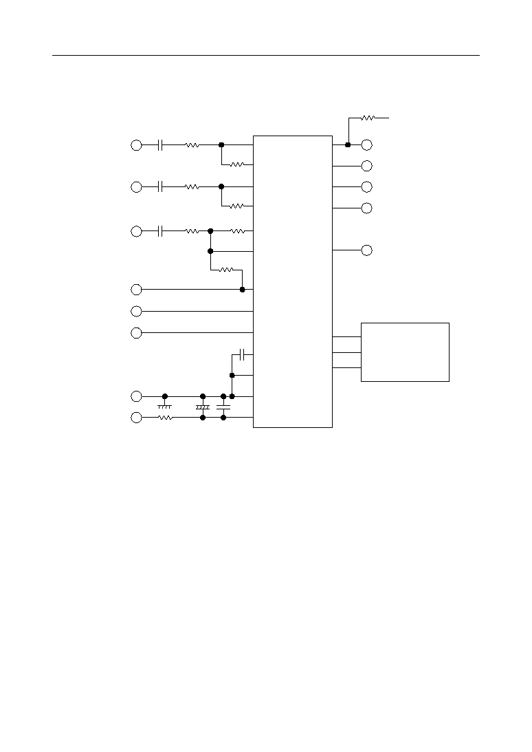
APPLICATION CIRCUIT
PCMOUT
PCMIN
MAIN
MAO
PBIN
0.1 mF
PCM output
PCM input
8 kHz SYNC pulse input
Power down control input
"1" = Operation
"0" = Power down
1 mF
20 kW
MSM7716
PBO
BCLK
SYNC
+3 V
PDN
AOUT≠
SGC
AG
DG
V
DD
0 V
+3 V
Microphone
analog input
Analog output*
DCLK
0 to 10 W
20 kW
1 mF
20 kW
Handset
analog input
20 kW
10 mF
VFO
PWI
1 mF
20 kW
Addition
signal input
20 kW
20 kW
AOUT+
Analog inverted
output*
AUXO
Auxiliary output*
1 kW
PCM shift clock input
DEN
CDIN
Controller
* The swing of the analog output signal is a maximum of ±1.0 V above and below the V
DD
/2 offset level.
1 mF
+
° Semiconductor
MSM7716
19/22
APPLICATION INFORMATION
Digital pattern for 0 dBm0
The digital pattern for 0 dBm0 is shown below.
(SYNC frequency = 8 kHz, signal frequency = 1 kHz)
Sample No.
S1
S2
S3
S4
S5
S6
S7
S8
MSD D2
D3
D4
D5
D6
D7
D8
D9 D10 D11 D12 D13 D14
0
0
0
0
1
1
1
1
0
1
1
0
1
0
0
1
1
0
0
1
0
1
1
0
0
1
1
0
1
0
0
1
0
0
0
0
1
1
1
1
0
0
0
0
1
1
1
1
1
1
1
1
0
0
0
0
0
1
1
0
1
0
0
1
1
1
1
1
0
0
0
0
0
0
0
0
1
1
1
1
1
1
1
1
0
0
0
0
0
1
1
0
1
0
0
1
1
1
1
1
0
0
0
0
1
0
0
1
0
1
1
0
SG
S1
S2
S3
S4
S5
S6
S7
S8

° Semiconductor
MSM7716
20/22
NOTES ON USE
∑ To ensure proper electrical characteristics, use bypass capacitors with excellent high frequency
characteristics for the power supply and keep them as close as possible to the device pins.
∑ Connect the AG pin and the DG pin as close as possible. Connect to the system ground with
low impedance.
∑ Mount the device directly on the board when mounted on PCBs. Do not use IC sockets. If the
use of IC socket is unavoidable, use the short lead type socket.
∑ When mounted on a frame, use electro-magnetic shielding, if any electro-magnetic wave
sources such as power supply transformers surround the device.
∑ Keep the voltage on the V
DD
pin not lower than ≠0.3 V even instantaneously to avoid latch-
up that may otherwise occur when power is turned on.
∑ Use a low noise (particularly, low level type of high frequency spike noise or pulse noise)
power supply to avoid erroneous operation and the degradation of the characteristics of these
devices.
° Semiconductor
MSM7716
21/22
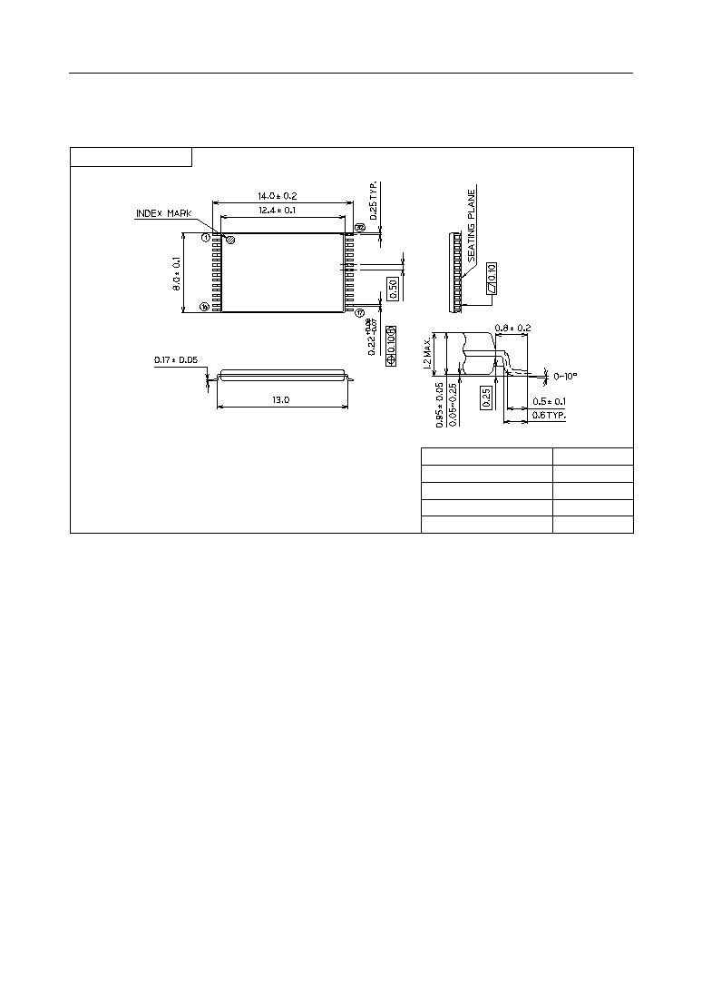
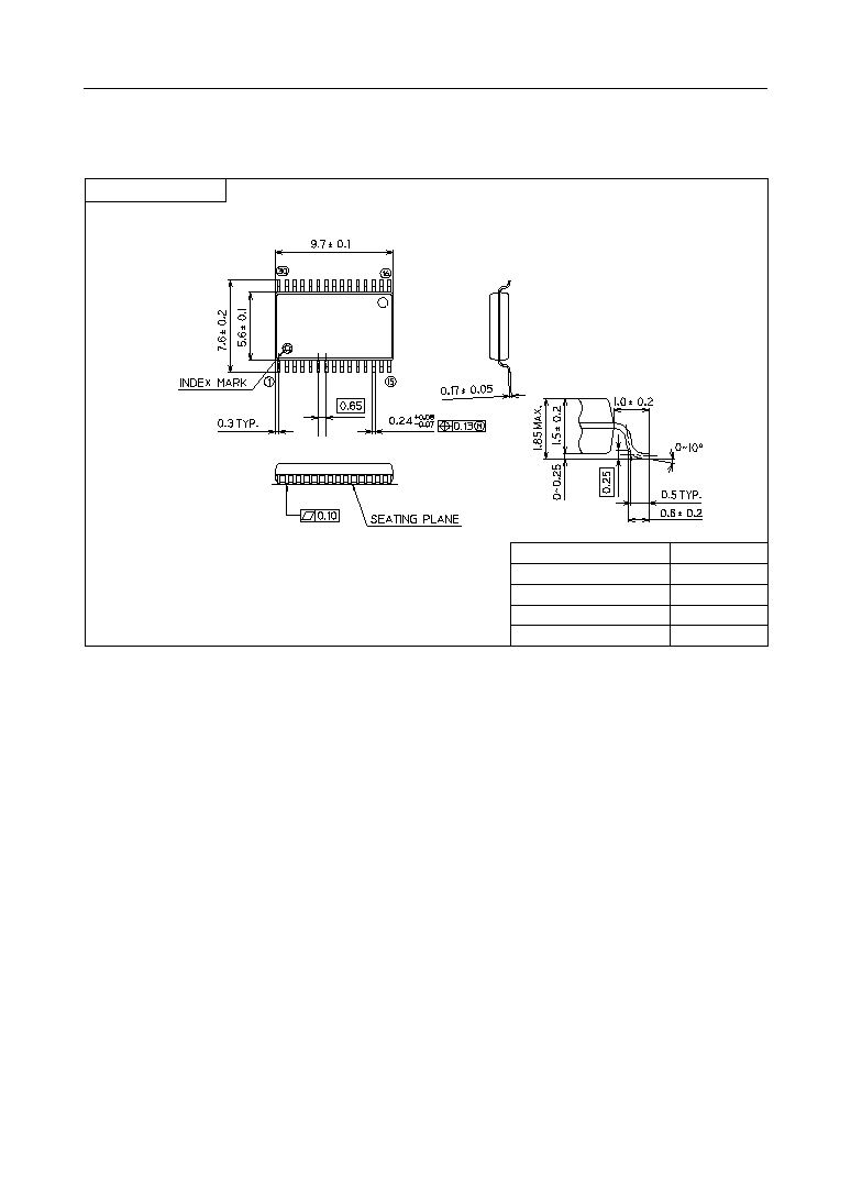
(Unit : mm)
PACKAGE DIMENSIONS
Notes for Mounting the Surface Mount Type Package
The SOP, QFP, TSOP, SOJ, QFJ (PLCC), SHP and BGA are surface mount type packages, which
are very susceptible to heat in reflow mounting and humidity absorbed in storage.
Therefore, before you perform reflow mounting, contact Oki's responsible sales person for the
product name, package name, pin number, package code and desired mounting conditions
(reflow method, temperature and times).
TSOPI32-P-814-0.50-1K
Package material
Lead frame material
Pin treatment
Solder plate thickness
Package weight (g)
Epoxy resin
42 alloy
Solder plating
5 mm or more
0.27 TYP.
Mirror finish
° Semiconductor
MSM7716
22/22
(Unit : mm)
Notes for Mounting the Surface Mount Type Package
The SOP, QFP, TSOP, SOJ, QFJ (PLCC), SHP and BGA are surface mount type packages, which
are very susceptible to heat in reflow mounting and humidity absorbed in storage.
Therefore, before you perform reflow mounting, contact Oki's responsible sales person for the
product name, package name, pin number, package code and desired mounting conditions
(reflow method, temperature and times).
SSOP30-P-56-0.65-K
Package material
Lead frame material
Pin treatment
Solder plate thickness
Package weight (g)
Epoxy resin
42 alloy
Solder plating
5 mm or more
0.19 TYP.
Mirror finish