
OKI Semiconductor
FEDL7716P-01
This issue: June 17, 2004
MSM7716P
Single Rail Linear CODEC
1/23
GENERAL DESCRIPTION
The MSM7716P is an extended temperature range version for the MSM7716 which is a single-channel CODEC
CMOS IC for voice signals that contains filters for linear A/D and D/A conversion.
Designed especially for a single-power supply and low-power applications, the device is optimized for
applications for the analog interfaces of audio signal processing DSPs and digital wireless systems.
The analog output signal can directly drive a ceramic type handset receiver. In addition, levels for analog outputs
can be set by external control.
FEATURES
� Single power supply
: +3.0V to +3.6 V
� Operating temperature
: -40�C to +85 �C
Remarks : Standard operating temperature range version MSM7716 (without "P")
- Power Supply Voltage : +2.7V to +3.6 V
- Operating temperature : -30�C to +85 �C
� Low power consumption
Operating mode
: 30 mW Typ.
Power down mode
: 0.05 mW Typ.
� Digital signal input/output interface : 14-bit serial code in 2's complement format
� Sampling frequency(fs)
: 4 to 16 kHz
� Transmission clock frequency
: fs
� 14 min., 2048 kHz max.
� Filter characteristics
: when fs = 8 kHz, complies with ITU-T Recommendation G. 714
� Built-in PLL eliminates a master clock
� Two input circuits in transmit section
� Two output circuits in receive section
� Transmit gain adjustable using an external resistor
� Receive gain adjustable by external control 8 steps, 4 dB/step
� Transmit mic-amp is eliminated by the gain setting of a maximum of 36 dB.
� Analog outputs can drive a load of a minimum of 1 k
; an amplitude of a maximum of 4.0 V
PP
with push-pull
driving.
� Built-in reference voltage supply
� Package options:
30-pin plastic SSOP (SSOP30-P-56-0.65-K) (MSM7716PMB)
FEDL7716P-01
OKI Semiconductor
MSM7716P
2/23
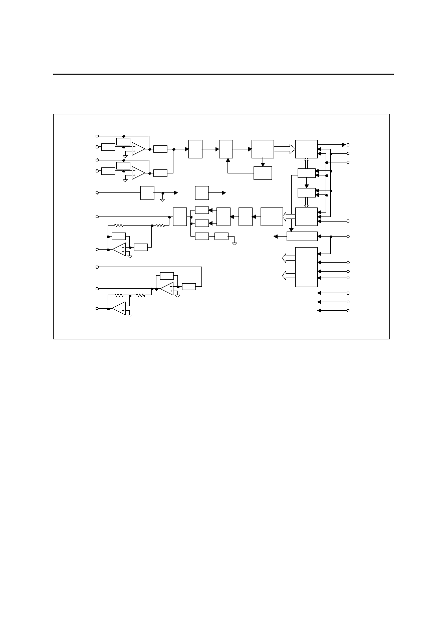
BLOCK DIAGRAM
SW1
SW2
RC
LPF
8th
BPF
14BIT
ADCONV
AUT O
ZERO
T CONT
PLL
RT IM
RCONT
PWD Logic
SG
GEN
VR
GEN
CONT
Logic
MAO
MAIN
PBO
PBIN
SGC
DG
AG
VDD
DCLK
CDIN
DEN
PDN
PCMIN
PCMOUT
SYNC
BCLK
SG
SG
SG
SG
SG
14BIT
DACONV
RC
LPF
5th
LPF
VOL
SW4
SW4
SW3
SW3
SW
CONT
VOL
CONT
PWD
VFO
AUXO
PWI
AOUT-
AOUT+
SW3
SW4
SW3
SW4
SW2
SW1
SW1
SW2

FEDL7716P-01
OKI Semiconductor
MSM7716P
3/23
PIN CONFIGURATION (TOP VIEW)
1
2
3
4
5
6
7
8
9
10
11
12
13
14
15
16
17
18
19
20
21
22
23
24
25
26
27
28
29
30
AG
AUXO
PWI
VFO
NC
NC
V
DD
DCLK
NC
DG
PCMI
SYNC
PDN
NC
NC
MAIN
MAO
PBIN
SGC
NC : No connect pin
AOUT+
AOUT�
NC
CDIN
DEN
NC
PBO
BCLK
NC
PCMOUT
NC
30-Pin Plastic SSOP
FEDL7716P-01
OKI Semiconductor
MSM7716P
4/23
PIN AND FUNCTIONAL DESCRIPTIONS
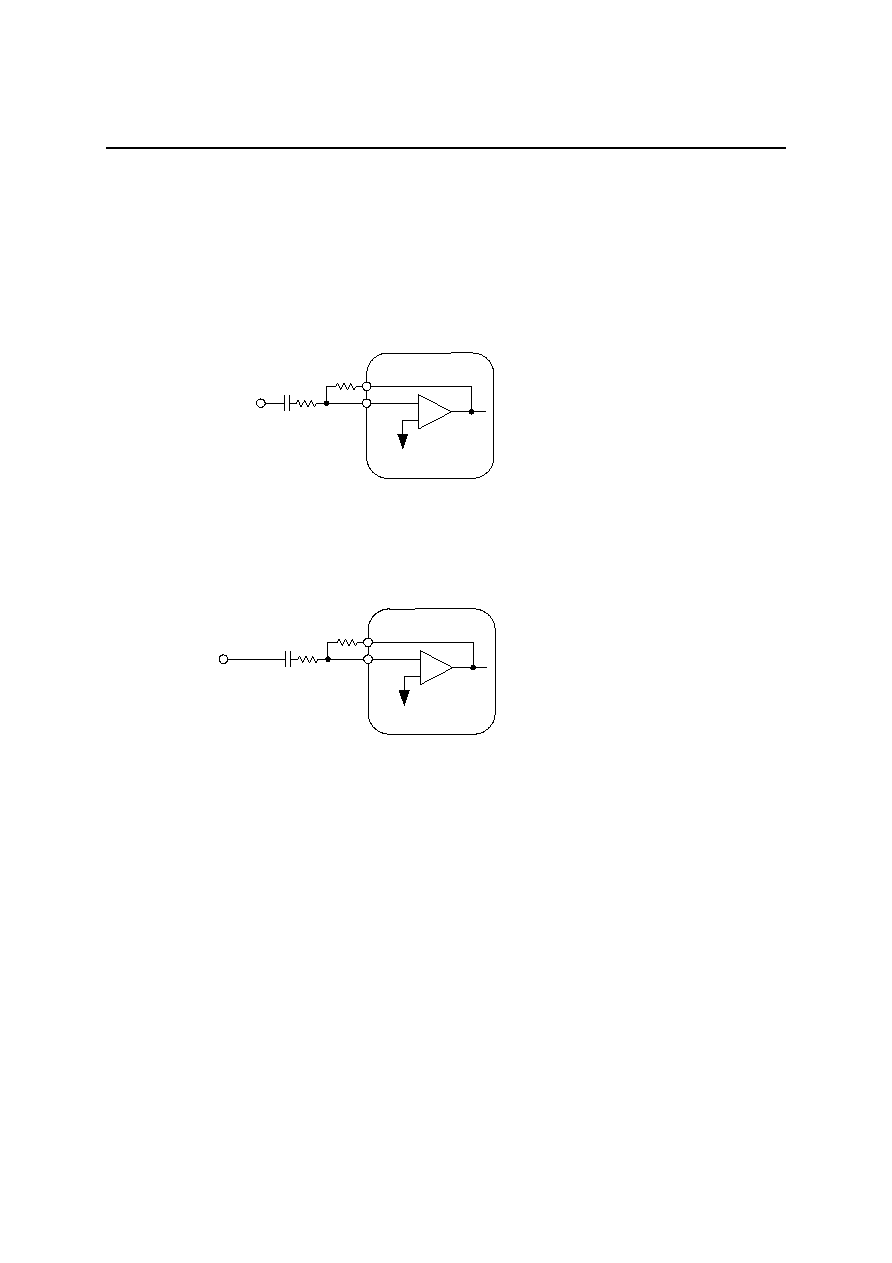
MAIN, MAO
Transmit microphone input and the level adjustment.
MAIN is connected to the noninverting input of the op-amp, and MAO is connected to the output of the op-amp.
The level adjustment should be configured as shown below.
During power saving and power down modes, the MAO output is in high impedance state.
PBIN, PBO
Transmit handset input and the level adjustment.
PBIN is connected to the noninverting input of the op-amp, and PBO is connected to the output of the op-amp. The
level adjustment should be configured as shown below.
During power saving and power down, the PBO output is in high impedance state.
V
DD
Power supply pin for +3.0 to 3.6 V (Typically 3.3 V).
AG
Analog signal ground.
DG
Ground pin for the digital signal circuits.
This ground is separated from the analog signal ground in this device. The DG pin must be connected to the AG pin
on the printed circuit board.
�
+
PBIN
C2
R3 : variable
R4 > 20 k
C2 > 1/ (2
�
3.14
�
30
�
R3) (F)
Gain = R4/R3 < 63
R4
PBO
R3
SG
Handset
microphone input
�
+
MAIN
C1
Microphone input
R2
MAO
R1
SG
R1 : variable
R2 > 20 k
C1 > 1/ (2
�
3.14
�
30
�
R3) (F)
Gain = R2/R1 < 63

FEDL7716P-01
OKI Semiconductor
MSM7716P
5/23
VFO
Receive filter output.
The output signal has an amplitude of 2.0 V
PP
above and below the signal ground voltage when the digital signal of
+3 dBm0 is input to PCMIN. VFO can drive a load of 20 k
or more.
This output can be externally controlled in the level range of 0 to �28 dB in 4 dB increments.
During power saving or power down, VFO output is at the voltage level (V
DD
/2) of SG with a high impedance
state.
PWI, AOUT+, AOUT�
PWI is connected to the inverting input of the receive driver.
The receive driver output is connected to the AOUT� pin. Thus, a receive level can be adjusted with the pins PWI,
AOUT�, and VFO described above.
The output of AOUT+ is inverted with respect to the output of AOUT� with a gain of 1.
The output signal amplitudes are a maximum of 2.0 V
PP
.
These outputs, above and below the signal ground voltage (V
DD
/2), can drive a load of a minimum of 1 k
with
push-pull driving (a load connected between AOUT+ and AOUT�).
The output amplitudes are 4 V
PP
maximum during push-pull driving. These outputs can be mute controlled
externally. These outputs are operational during power saving and output the SG voltage (V
DD
/2) in the high
impedance state.
AUXO
Auxiliary receive filter output.
The output signal is inverted with respect to the VFO output with a gain of 1. The output signal swings above and
below the SG voltage (V
DD
/2), and can drive a minimum load of 0.5 k
with respect to the SG voltage.
The output can be mute controlled externally.
During power saving and power down, AUXO outputs the SG voltage (V
DD
/2) in the high impedance state.
BCLK
Shift clock signal input for PCMIN and PCMOUT.
The frequency is equal to the data rate. Setting this signal to logic "1" or "0" drives both transmit and receive
circuits to the power-saving state.

FEDL7716P-01
OKI Semiconductor
MSM7716P
6/23
SYNC
Synchronizing signal input.
In the transmit section, the PCM output signal from the PCMOUT pin is output synchronously with this
synchronizing signal. This synchronizing signal triggers the PLL and synchronizes all timing signals of the
transmit section.
In the receive section, 14 bits required are selected from serial input of PCM signals on the PCMIN pin by the
synchronizing signal.
Signals in the receive section are synchronized by this synchronizing signal. This signal must be synchronized in
phase with the BCLK.
When this signal frequency is 8 kHz, the transmit and receive section have the frequency characteristics specified
by ITU-T G. 714. The frequency characteristics for 8 kHz are specified in this data sheet.
For different frequencies of the SYNC signal, the frequency values in this data sheet should be translated
according to the following equation:
Frequency values described in the data sheet
8 kHz
� the SYNC frequency values to be actually used
Setting this signal to logic "1" or "0" drives the device to power-saving state.
PCMIN
PCM signal input.
A serial PCM signal input to this pin is converted to an analog signal synchronously with the SYNC signal and
BCLK signal.
The data rate of the PCM signal is equal to the frequency of the BCLK signal.
The PCM signal is shifted at a falling edge of the BCLK signal. The PCM signal is latched into the internal register
when shifted by 14 bits.
The top of the data (MSD) is identified at the rising edge of SYNC.
The input signal should be input in the 14-bit 2's complement format.
The MSD bit represents the polarity of the signal with respect to the signal ground.
FEDL7716P-01
OKI Semiconductor
MSM7716P
7/23
PCMOUT
PCM signal output.
The PCM output signal is output from MSD in sequential order, synchronously with the rising edge of the BCLK
signal.
MSD may be output at the rising edge of the SYNC signal, depending on the timing between BCLK and SYNC.
This pin is in high impedance state except during 14-bit PCM output, and is in either in high impedance or in "L"
output state during power down and power saving mode.
A pull-up resistor must be connected to this pin, because its output is configured as an open drain.
The output coding format is in 14-bit 2's complement.
The MSD represents a polarity of the signal with respect to the signal ground.
Table 1
Input/Output Level
PCMIN/PCMOUT
MSD
+Full scale
0 1 1 1 1 1 1 1 1 1 1 1 1 1
+1
0 0 0 0 0 0 0 0 0 0 0 0 0 1
0
0 0 0 0 0 0 0 0 0 0 0 0 0 0
�1
1 1 1 1 1 1 1 1 1 1 1 1 1 1
�Full
scale
1 0 0 0 0 0 0 0 0 0 0 0 0 0
PDN
Power down control signal input.
A digital "L" level drives both transmit and receive circuits to a power down state.
The control registers are set to the initial state.
Be sure to initialize the control registers by to execute this power down by keeping this pin to digital '0' level for
100 ns or longer after the power is turned on the power and the V
DD
exceeds 3.0 V.
SGC
Connection of a bypass capacitor for generating the signal ground voltage level.
Connect a 0.1
�F capacitor with excellent high frequency characteristics between the AG pin and the SGC pin.
FEDL7716P-01
OKI Semiconductor
MSM7716P
8/23
DEN, DCLK, CDIN
Serial control ports for the microcontroller interface.
Writing data to the 8-bit control register enables control of the receive output level and the signal path.
DEN is the "Enable" signal pin, DCLK is the data shift clock input pin, and CDIN is the control data input pin.
When powered down (PDN = 0), the initial values are set as shown in Tables 2, 3, and 4. The initial values are held
unless the control data is written after power-down release.
The control data is shifted at the rising edge of the DCLK signal and latched into the internal control register at the
rising edge of the DEN signal.
When the microcontroller interface is not used, these pins should be connected to DG.
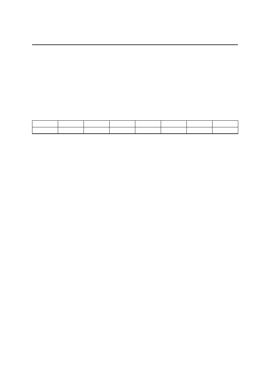
The bit map of the 8-bit control register is shown below.
B7 B6 B5 B4 B3 B2 B1 B0
SW1 SW2 SW3 SW4 -- VOL1 VOL2 VOL3
FEDL7716P-01
OKI Semiconductor
MSM7716P
9/23
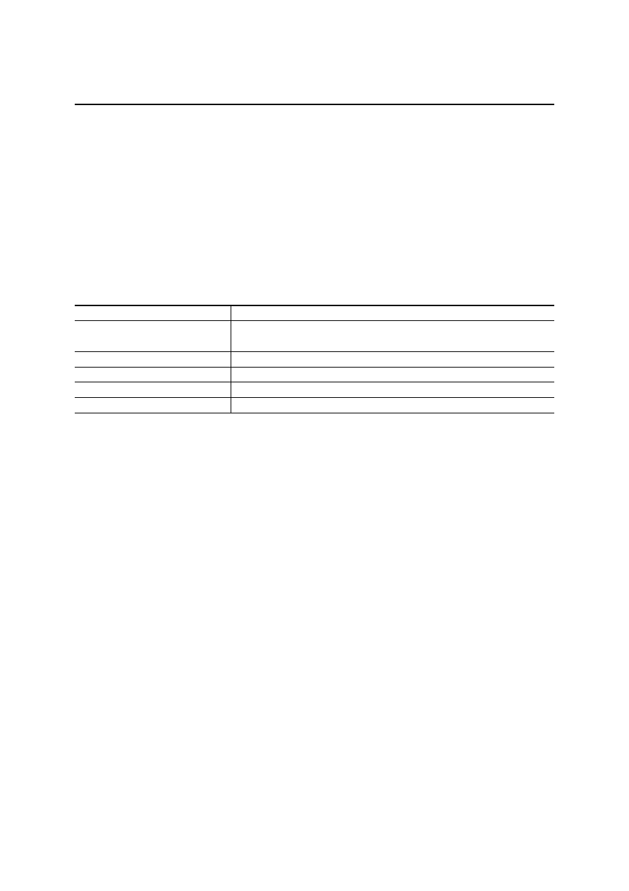
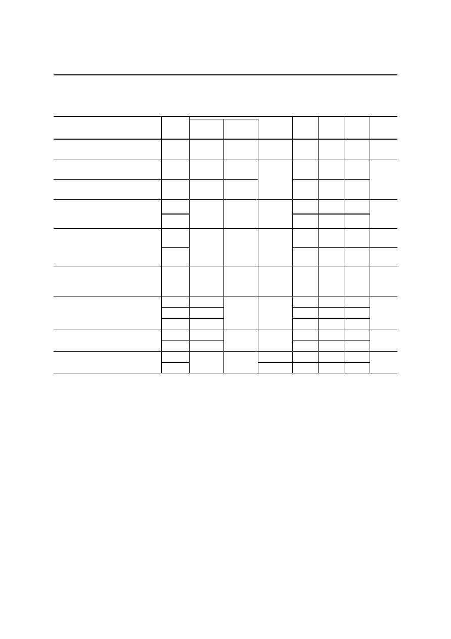
ABSOLUTE MAXIMUM RATINGS
Parameter Symbol
Condition
Rating Unit
Power Supply Voltage
V
DD
AG = DG = 0 V
�0.3 to +7.0
V
Analog Input Voltage
V
AIN
AG = DG = 0 V
�0.3 to V
DD
+0.3
V
Digital Input Voltage
V
DIN
AG = DG = 0 V
�0.3 to V
DD
+0.3
V
Storage Temperature
T
STG
--
�55 to +150
�C
RECOMMENDED OPERATING CONDITIONS
Parameter Symbol
Condition Min.
Typ.
Max.
Unit
Power Supply Voltage
V
DD
--
3.0 3.3 3.6 V
Operating Temperature
Ta
--
�40
+25
+85
�C
Analog Input Voltage
V
AIN
Gain = 1
--
--
1.4
V
PP
High Level Input Voltage
V
IH
0.45
�
V
D
D
-- V
DD
V
Low Level Input Voltage
V
IL
SYNC, BCLK, PCMIN, PDN,
DEN, DCLK, CDIN
0 --
0.16
�
V
D
D
V
Clock Frequency
F
C
BCLK
14
�
F
S
-- 128
�
F
S
kHz
Sync Pulse Frequency
F
S
SYNC
4.0
8.0
16 kHz
Clock Duty Ratio
D
C
BCLK
40 50 60
%
Digital Input Rise Time
t
lr
--
--
50
ns
Digital Input Fall Time
t
lf
SYNC, BCLK, PCMIN, PDN,
DEN, DCLK, CDIN
-- -- 50
ns
t
XS
, t
RS
BCLK
SYNC, See Fig. 1
100
--
--
ns
Sync Pulse Setting Time
t
SX
, t
SR
SYNC
BCLK, See Fig. 1
100
--
--
ns
High Level Sync Pulse Width *1
t
WSH
SYNC, See Fig. 1
1 BCLK
--
--
--
Low Level Sync Pulse Width *1
t
WSL
SYNC, See Fig. 1
1 BCLK
--
--
--
PCMIN Setup Time
t
DS
Refer to Fig. 1
100
--
--
ns
PCMIN Hold Time
t
DH
Refer to Fig. 1
100
--
--
ns
R
DL
Pull-up
resistor
0.5
--
--
k
Digital Output Load
C
DL
-- --
--
100
pF
t
WCL
DCLK Low width, See Fig. 2
50
--
--
DCLK Pulse Width
t
WCH
DCLK High width, See Fig. 2
50
--
--
ns
t
CDL
DCLK
DEN, See Fig. 2
50
--
--
DEN Setting Time 1
t
DCL
DEN
DCLK, See Fig. 2
50
--
--
ns
t
CDH
DCLK
DEN, See Fig. 2
50
--
--
DEN Setting Time 2
t
DCH
DEN
DCLK, See Fig. 2
50
--
--
ns
CDIN Setup Time
t
CDS
See Fig. 2
50
--
--
CDIN Hold Time
t
CDH
See Fig. 2
50
--
--
ns
Transmit gain stage, Gain = 0 dB
�100 -- +100
mV
Analog Input Allowable DC Offset
V
off
Transmit gain stage, Gain = 20 dB
�10 -- +10
mV
Allowable Jitter Width
--
SYNC, BCLK
--
--
1000
ns
*1 For example, the minimum pulse width of SYNC is 488 ns when the frequency of BCLK is 2048 kHz.
FEDL7716P-01
OKI Semiconductor
MSM7716P
10/23
RECOMMENDED OPERATING CONDITIONS (Continued)
Parameter Symbol
Condition Min.
Typ.
Max.
Unit
t
SD
20
--
100
t
XD1
20
--
100
t
XD2
20
--
100
Digital Output Delay Time
t
XD3
CL = 50 pF + 1 LSTTL
Pull-up resistor = 500
20 -- 100
ns
ELECTRICAL CHARACTERISTICS
DC and Digital Interface Characteristics
(Fs = 8 kHz, V
DD
= 3.0 to 3.6 V, Ta = �40 to +85�C)
Parameter Symbol
Condition Min. Typ. Max.
Unit
V
DD
= 3.6 V
--
10.0
17.0
I
DD1
Operating mode
No signal
V
DD
= 3.0 V
--
8.0
13.0
mA
I
DD2
Power-saving mode, PDN = 1,
SYNC, BCLK
OFF
-- 6.0 11.0
mA
Power Supply Current
I
DD3
Power-down mode, PDN = 0
--
0.01
0.05
mA
High Level Input Voltage
V
IH
0.45
�
V
D
D
-- V
DD
V
Low Level Input Voltage
V
IL
SYNC, BCLK, PCMIN, DEN,
CDIN, DCLK, PDN
0.0 --
0.16
�
V
D
D
V
High Level Input Leakage Current
I
IH
-- --
--
2.0
�
A
Low Level Input Leakage Current
I
IL
-- --
--
0.5
�
A
Digital Output Low Voltage
V
OL
PCMOUT pull-up resistor = 500
0.0 0.2 0.4 V
Digital Output Leakage Current
I
O
-- --
--
10
�
A
Input Capacitance
C
IN
-- --
5
--
pF

FEDL7716P-01
OKI Semiconductor
MSM7716P
11/23
Transmit Analog Interface Characteristics
(Fs = 8 kHz, V
DD
= 3.0 to 3.6 V, Ta = �40 to +85�C)
Parameter Symbol
Condition Min. Typ. Max.
Unit
Input Resistance
R
INX
MAIN,
PBIN
10
--
-- M
Output Load Resistance
R
LGX
20
--
--
k
Output Load Capacitance
C
LGX
--
--
30
pF
Output Amplitude
V
OGX
MAO, PBO with respect to SG
�0.7 -- +0.7
V
Offset Voltage
V
OSGX
Gain = 1
�20
--
+20
mV
Receive Analog Interface Characteristics
(Fs = 8 kHz, V
DD
= 3.0 to 3.6 V, Ta = �40 to +85�C)
Parameter Symbol
Condition Min. Typ. Max.
Unit
R
OAO
AUXO, AOUT+, AOUT�
--
--
10
Output Resistance
R
OVO
VFO
--
--
100
R
LAO
AUXO, AOUT+, AOUT�
(each) with respect to SG
0.5 -- --
k
Output Load Resistance
R
LVO
VFO with respect to SG
20
--
--
k
Output Load Capacitance
C
LAO
Output
open
--
--
50
pF
Output Amplitude
V
OAO
AUXO, AOUT+, AOUT�, VFO
with respect to SG
�1.0 -- +1.0
V
Offset Voltage
V
OSA
AUXO, AOUT+, AOUT�, VFO
with respect to SG
�100 -- +100
mV
FEDL7716P-01
OKI Semiconductor
MSM7716P
12/23
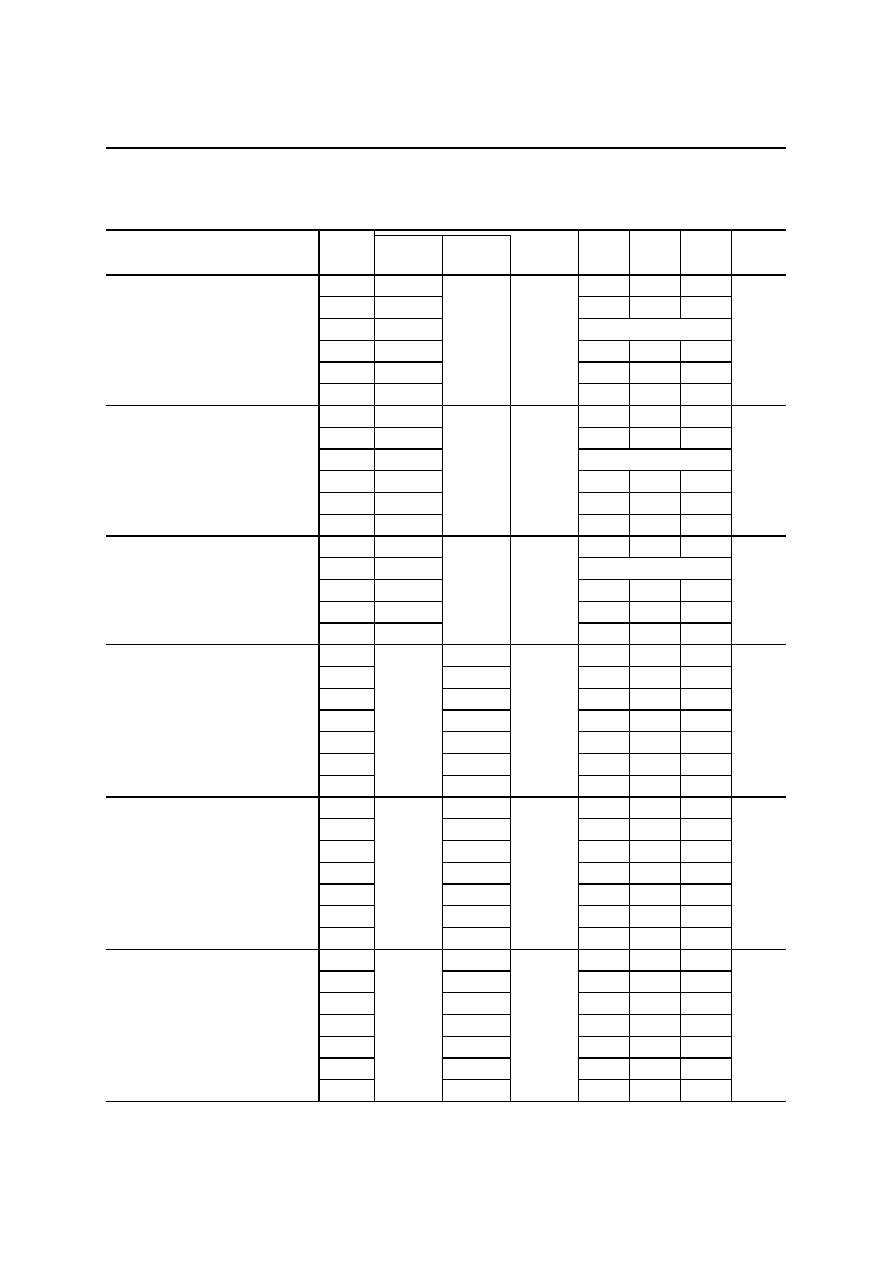
AC Characteristics
(F
S
= 8 kHz, V
DD
= 3.0 to 3.6 V, Ta = �40 to +85�C)
Parameter Symbol
Freq.
(Hz)
Level
(dBm0)
Condition Min. Typ. Max. Unit
Loss 1
60
20
--
--
Loss 2
300
�0.2
--
+0.4
Loss 3
1020
Reference
Loss 4
2020
�0.2
--
+0.4
Loss 5
3000
�0.2
--
+0.4
Overall Frequency Response
Loss 6
3400
0
Analog
to
Analog
0 -- 1.6
dB
Loss T1
60
20
--
--
Loss T2
300
�0.15
--
+0.2
Loss T3
1020
Reference
Loss T4
2020
�0.15
--
+0.2
Loss T5
3000
�0.15
--
+0.2
Transmit Frequency Response
(Expected Value)
Loss T6
3400
0
0 -- 0.8
dB
Loss R1
300
�0.15
--
+0.2
Loss R2
1020
Reference
Loss R3
2020
�0.15
--
+0.2
Loss R4
3000
�0.15
--
+0.2
Receive Frequency Response
(Expected Value)
Loss R5
3400
0
0.0 -- 0.8
dB
SD 1
3
55.9
--
--
SD 2
0
55.9
--
--
SD 3
�10
55.9
--
--
SD 4
�20
45.9
--
--
SD 5
�30
35.9
--
--
SD 6
�40
25.9
--
--
Overall Signal to Distortion Ratio
SD 7
1020
�50
Analog
to
Analog
*1
15.9 -- --
dB
SD T1
3
58
--
--
SD T2
0
58
--
--
SD T3
�10
58
--
--
SD T4
�20
48
--
--
SD T5
�30
38
--
--
SD T6
�40
28
--
--
Transmit Signal to Distortion Ratio
(Expected Value)
SD T7
1020
�50
*1
18 -- --
dB
SD R1
3
58
--
--
SD R2
0
58
--
--
SD R3
�10
58
--
--
SD R4
�20
48
--
--
SD R5
�30
38
--
--
SD R6
�40
28
--
--
Receive Signal to Distortion Ratio
(Expected Value)
SD R7
1020
�50
*1
18 -- --
dB
*1 Psophometric filter is used.
FEDL7716P-01
OKI Semiconductor
MSM7716P
13/23
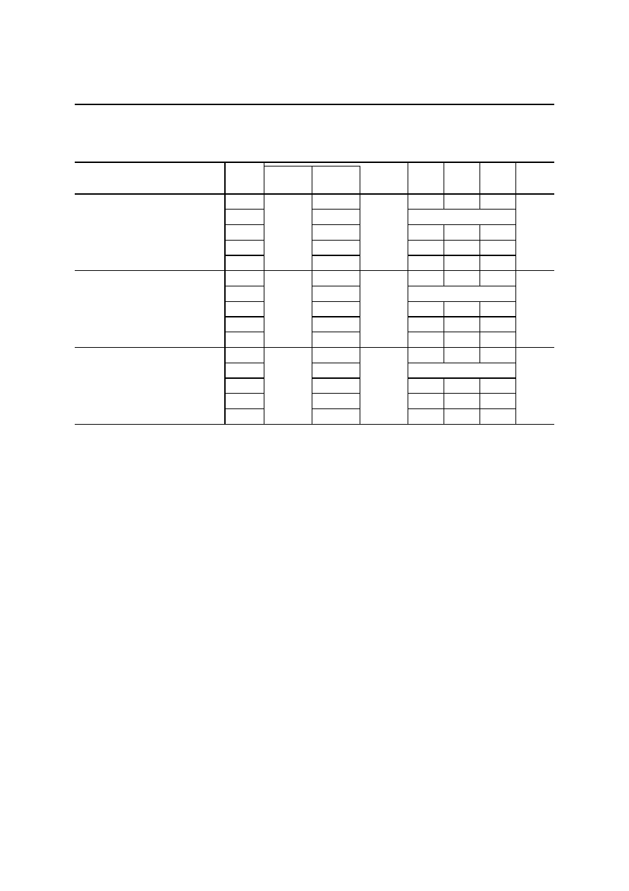
AC Characteristics (Continued)
(F
S
= 8 kHz, V
DD
= 3.0 to 3.6 V, Ta = �40 to +85�C)
Parameter Symbol
Freq.
(Hz)
Level
(dBm0)
Condition Min. Typ. Max. Unit
GT 1
3
�0.4
+0.01
+0.4
GT 2
�10
Reference
GT 3
�40
�0.3
0.00
+0.8
GT 4
�50
�1.3
�0.03
+1.3
Overall Gain Tracking
GT 5
1020
�55
Analog
to
Analog
�1.6 �0.15 +1.6
dB
GT T1
3
�0.3
+0.01
+0.3
GT T2
�10
Reference
GT T3
�40
�0.3
0.00
+0.3
GT T4
�50
�0.6
�0.03
+0.6
Transmit Gain Tracking
(Expected Value)
GT T5
1020
�55
�1.2 +0.15 +1.2
dB
GT R1
3
�0.3
�0.06
+0.3
GT R2
�10
Reference
GT R3
�40
�0.3
�0.02
+0.3
GT R4
�50
�0.6
�0.02
+0.6
Receive Gain Tracking
(Expected Value)
GT R5
1020
�55
�1.2 �0.27 +1.2
dB
FEDL7716P-01
OKI Semiconductor
MSM7716P
14/23
AC Characteristics (Continued)
(F
S
= 8 kHz, V
DD
= 3.0 to 3.6 V, Ta = �40 to +85�C)
Parameter Symbol
Freq.
(Hz)
Level
(dBm0)
Condition Min. Typ. Max. Unit
Overall Idle Channel Noise
Nidle A
--
--
AIN: no signal
*1
-- �70 �66
dBm0p
Transmit Idle Channel Noise
(Expected Value)
Nidle T
--
--
--
�71
�67
Receive Idle Channel Noise
(Expected Value)
Nidle R
--
--
AIN: no signal
*1
-- �76 �74
dBm0p
AV T
0.338 0.350 0.362
Absolute Level (Initial Level)
AV R
1020 0
V
DD
=3.0 V
Ta=25�C
*2
0.483 0.500 0.518
Vrms
AV Tt
�0.2
--
+0.2
dB
Absolute Level
(Deviation of Temperature and
Power)
AV Rt
V
DD
= +3.0
to 3.6 V
Ta = �40
to 85�C
�0.2 -- +0.2 dB
Absolute Delay
t
D
1020 0
A to A
BCLK
= 64 kHz
-- -- 0.6 ms
t
GD
T1
500
--
--
0.325
t
GD
T2 600 to 2600
-- --
0.175
Transmit Group Delay
t
GD
T3
2800
0 *3
-- --
0.325
ms
t
GD
R1 500 to 2600
-- 0.00
0.125
Receive Group Delay
t
GD
R2
2800
0 *3
-- 0.12
0.325
ms
CR T
TRANS
RECV
75 85 --
Crosstalk Attenuation
CR R
1020 0
RECV
TRANS
70 80 --
dB
*1 Psophometric filter is used.
*2 AVT is defined at MAO and PBO-PCMOUT.
AVR is defined at PCMIN-VFO.
VOL = 0 dB
*3 Minimum value of the group delay distortion
FEDL7716P-01
OKI Semiconductor
MSM7716P
15/23
AC Characteristics (Continued)
(F
S
= 8 kHz, V
DD
= 3.0 to 3.6 V, Ta = �40 to +85�C)
Parameter Symbol
Freq.
(Hz)
Level
(dBm0)
Condition Min. Typ. Max. Unit
Discrimination DIS
4.6 to
72 kHz
0
0 to
4000 Hz
30 32 -- dB
Out-of-band Spurious
S
300 to
3400
0
4.6 to 100
kHz
-- �37.5 �35 dBm0
Intermodulation Distortion
IMD
fa = 470
fb = 320
�4
2fa � fb
--
�52
�40
dBm0
PSR T
Power Supply Noise Rejection
Ratio
PSR R
0 to
50 kHz
50 mV
PP
*1 -- 30 -- dB
Auxiliary Output Gain
G
AUX
1020
0
VFO to AUXO
�1.0 0 +1.0 dB
G
V2
Set at �4 dB
�5 �4 �3
G
V3
�8
dB �9 �8 �7
G
V4
�12 dB �13 �12 �11
G
V5
�16 dB �17 �16 �15
G
V6
�20 dB �21 �20 �19
G
V7
�24 dB �25 �24 �23
VOL Gain Setting Value
G
V8
1020 0 Referenced
to 0 dB
setting
�28 dB �29 �28 �27
dB
*1 Measured inband.
FEDL7716P-01
OKI Semiconductor
MSM7716P
16/23
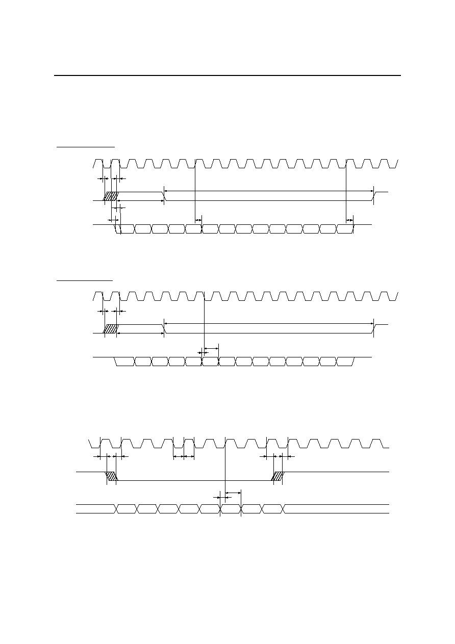
TIMING DIAGRAM
PCM Data Output Timing
Figure 1 Basic Timing Diagram
MCU Interface Timing
Figure 2 MCU Interface Timing Diagram
BCLK
1
2
3
4
5
6
7
8
9
10
SYNC
PCMOUT
D9
D10
D11
D12
D13
D14
MSD
t
XS
t
SX
t
WSH
t
SD
t
XD1
t
XD2
t
XD3
BCLK
SYNC
PCMIN
Transmit Timing
Receive Timing
11
When t
XS
1/2 � Fc, the Delay of the MSD bit is defined as t
XD1
.
When t
SX
< 1/2 � Fc, the Delay of the MSD bit is defined as t
SD
.
12
13
14
15
16
17
D2
D3
D4
D5
D6
D7
D8
1
2
3
4
5
6
7
8
9
10
D9
D10
D11
D12
D13
D14
MSD
t
RS
t
SR
t
WSH
t
DS
11
12
13
14
15
16
17
D2
D3
D4
D5
D6
D7
D8
t
DH
t
WSL
t
WSL
t
CDL
t
DCL
t
CDH
t
DCH
t
WCH
t
WCL
DCLK
1
2
3
4
5
6
7
8
9
10
11
12
13
DEN
B3
B4
B5
B6
B7
B2
B1
B0
CDIN
t
CDH
t
CDS
FEDL7716P-01
OKI Semiconductor
MSM7716P
17/23
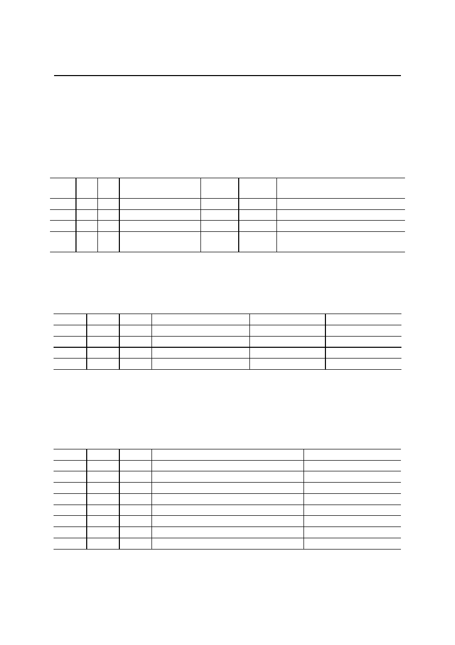
FUNCTIONAL DESCRIPTION
Control Data Description
SW1, SW2������Control bits for the transmit speech path switch.
The AD converter input is selected according to the bit data shown in Table 2.
Table 2
State SW
2
SW
1
AD Converter Input
MAO
Output
PBO
Output
Remarks
T1
0
0
No signal (muting state)
SG
SG
--
T2
0
1
Input signal to MAIN
Effective
SG
At initial setting
T3
1
0
Input signal to PBIN
SG
Effective
--
T4
1
1
Addition signal of both
MAIN and PBIN
Effective
Effective
The gain of each input drops by 6dB
SW3, SW4������Control bits for the receive speech path switch.
The control should be performed according to Table 3.
Table 3
State
SW4
SW3
AOUT+, AOUT� Output AUXO
Output
Remarks
R1 0 0
SG
SG
--
R2
0
1
PWI
SG
At initial setting
R3 1 0
SG
DA
--
R4 1 1
PWI
DA
--
DA: DA converter output.
SG: signal ground voltage.
VOL1, VOL2, VOL3��������Control bits for the receive signal output level.
By controlling these bits, the output levels of VFO and AUXO can be controlled
according to Table 4.
Table 4
VOL1 VOL2 VOL3
Receive
Signal
Gain
Remarks
0
0
0
0 dB
At initial setting
0 0 1
�4
dB
--
0 1 0
�8
dB
--
0 1 1
�12
dB
--
1 0 0
�16
dB
--
1 0 1
�20
dB
--
1 1 0
�24
dB
--
1 1 1
�28
dB
--
FEDL7716P-01
OKI Semiconductor
MSM7716P
18/23
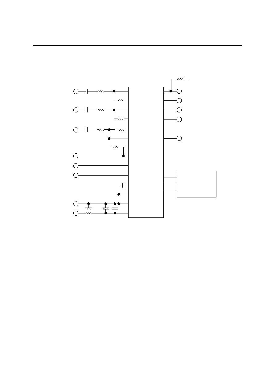
APPLICATION CIRCUIT
* The swing of the analog output signal is a maximum of �1.0 V above and below the V
DD
/2 offset level.
PCMOUT
PCMIN
MAIN
MAO
PBIN
0.1
�
F
PCM output
PCM input
8 kHz SYNC pulse input
Power down control input
"1" = Operation
"0" = Power down
1
�
F 20 k
MSM7716
P
PBO
BCLK
SYNC
+3
.3
V
PDN
AOUT
SGC
AG
DG
V
DD
0 V
+3
.3
V
Microphone
analog input
Analog output*
DCLK
0 to 10
20 k
1
�
F 20 k
Handset
analog input
20 k
10
�
F
VFO
PWI
1
�
F 20 k
Addition
signal input
20 k
20 k
AOUT
Analog inverted
output*
AUXO
Auxiliary output*
1 k
PCM shift clock input
DEN
CDIN
Controller
1
�
F
+
FEDL7716P-01
OKI Semiconductor
MSM7716P
19/23
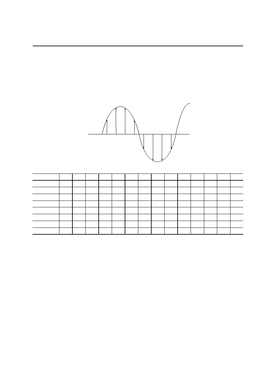
APPLICATION INFORMATION
Digital pattern for 0 dBm0
The digital pattern for 0 dBm0 is shown below.
(SYNC frequency = 8 kHz, signal frequency = 1 kHz)
Sample
No.
MSD D2 D3 D4 D5 D6 D7 D8 D9 D10 D11
D12 D13
D14
S1
0 0 1 0 0 0 1 0 1 0 1 0 1 1
S2
0 1 0 1 0 0 1 1 1 0 1 1 1 0
S3
0 1 0 1 0 0 1 1 1 0 1 1 1 0
S4
0 0 1 0 0 0 1 0 1 0 1 0 1 1
S5
1 1 0 1 1 1 0 1 0 1 0 1 0 0
S6
1 0 1 0 1 1 0 0 0 1 0 0 0 1
S7
1 0 1 0 1 1 0 0 0 1 0 0 0 1
S8
1 1 0 1 1 1 0 1 0 1 0 1 0 0
SG
S1
S2
S3
S4
S5
S6
S7
S8

FEDL7716P-01
OKI Semiconductor
MSM7716P
20/23
NOTES ON USE
� To ensure proper electrical characteristics, use bypass capacitors with excellent high frequency characteristics for
the power supply and keep them as close as possible to the device pins.
� Connect the AG pin and the DG pin as close as possible. Connect to the system ground with low impedance.
� Mount the device directly on the board when mounted on PCBs. Do not use IC sockets. If the use of IC socket is
unavoidable, use the short lead type socket.
� When mounted on a frame, use electro-magnetic shielding, if any electro-magnetic wave sources such as power
supply transformers surround the device.
� Keep the voltage on the V
DD
pin not lower than �0.3 V even instantaneously to avoid latch-up that may otherwise
occur when power is turned on.
� Use a low noise (particularly, low level type of high frequency spike noise or pulse noise) power supply to avoid
erroneous operation and the degradation of the characteristics of these devices.
FEDL7716P-01
OKI Semiconductor
MSM7716P
21/23
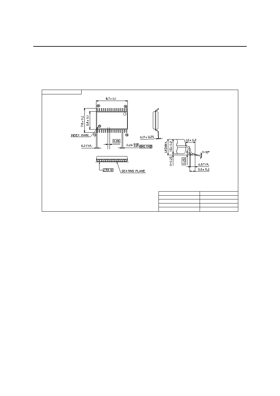
PACKAGE DIMENSIONS
SSOP30-P-56-0.65-K
Mirror finish
Package material
Epoxy resin
Lead frame material
42 alloy
Pin treatment
Solder plating (
5�m)
Package weight (g)
0.19 TYP.
5
Rev. No./Last Revised
5/Dec. 5, 1996
Notes for Mounting the Surface Mount Type Package
The surface mount type packages are very susceptible to heat in reflow mounting and humidity
absorbed in storage.
Therefore, before you perform reflow mounting, contact Oki's responsible sales person for the product
name, package name, pin number, package code and desired mounting conditions (reflow method,
temperature and times).
(Unit: mm)

FEDL7716P-01
OKI Semiconductor
MSM7716P
22/23
REVISION HISTORY
Page
Document
No.
Date
Previous
Edition
Current
Edition
Description
FEDL7716P-01
Jun. 17, 2004
�
�
First edition

FEDL7716P-01
OKI Semiconductor
MSM7716P
23/23
NOTICE
1. The information contained herein can change without notice owing to product and/or technical improvements.
Before using the product, please make sure that the information being referred to is up-to-date.
2. The outline of action and examples for application circuits described herein have been chosen as an
explanation for the standard action and performance of the product. When planning to use the product, please
ensure that the external conditions are reflected in the actual circuit, assembly, and program designs.
3. When designing your product, please use our product below the specified maximum ratings and within the
specified operating ranges including, but not limited to, operating voltage, power dissipation, and operating
temperature.
4. Oki assumes no responsibility or liability whatsoever for any failure or unusual or unexpected operation
resulting from misuse, neglect, improper installation, repair, alteration or accident, improper handling, or
unusual physical or electrical stress including, but not limited to, exposure to parameters beyond the specified
maximum ratings or operation outside the specified operating range.
5. Neither indemnity against nor license of a third party's industrial and intellectual property right, etc. is
granted by us in connection with the use of the product and/or the information and drawings contained herein.
No responsibility is assumed by us for any infringement of a third party's right which may result from the use
thereof.
6. The products listed in this document are intended for use in general electronics equipment for commercial
applications (e.g., office automation, communication equipment, measurement equipment, consumer
electronics, etc.). These products are not, unless specifically authorized by Oki, authorized for use in any
system or application that requires special or enhanced quality and reliability characteristics nor in any
system or application where the failure of such system or application may result in the loss or damage of
property, or death or injury to humans.
Such applications include, but are not limited to, traffic and automotive equipment, safety devices, aerospace
equipment, nuclear power control, medical equipment, and life-support systems.
7. Certain products in this document may need government approval before they can be exported to particular
countries. The purchaser assumes the responsibility of determining the legality of export of these products
and will take appropriate and necessary steps at their own expense for these.
8.
No part of the contents contained herein may be reprinted or reproduced without our prior permission.
Copyright 2004 Oki Electric Industry Co., Ltd.