 | –≠–ª–µ–∫—Ç—Ä–æ–Ω–Ω—ã–π –∫–æ–º–ø–æ–Ω–µ–Ω—Ç: MSM7730 | –°–∫–∞—á–∞—Ç—å:  PDF PDF  ZIP ZIP |

D
ATA
S
HEET
MSM7730
Wireless LAN Baseband Controller
June 1998
O K I L O G I C P R O D U C T S

s
s
≠≠≠≠≠≠≠≠≠≠≠≠≠≠≠≠≠≠≠≠≠≠≠≠≠≠≠≠≠≠≠≠≠≠≠≠≠≠≠≠≠≠≠≠≠≠≠≠≠≠≠≠≠≠≠≠≠≠≠≠≠≠≠≠≠≠≠≠≠≠≠≠≠≠≠≠≠≠≠≠≠≠≠≠≠≠≠≠≠≠≠
0
Oki Semiconductor
Description ................................................................................................................................................................3
Features .....................................................................................................................................................................3
Block Diagram .......................................................................................................................................................... 4
Interface Descriptions ..............................................................................................................................................4
Processor Interface .............................................................................................................................................4
Shared RAM Interface .......................................................................................................................................5
EEPROM Interface .............................................................................................................................................6
Host Interface (Between Adapter Card and Computer or Laptop) .....................................................6
Radio Interface ...................................................................................................................................................7
MODEM Interface .............................................................................................................................................8
Modulator .....................................................................................................................................................8
Demodulator ................................................................................................................................................9
PHY Interface ...................................................................................................................................................10
PCMCIA Interface ...........................................................................................................................................11
Pin Configuration................................................................................................................................................... 12
Pin Descriptions ..................................................................................................................................................... 13
MSM7730 Register MAP ....................................................................................................................................... 17
1
Oki Semiconductor
MSM7730
Wireless LAN Baseband Controller
DESCRIPTION
The MSM7730 is Oki's second generation of wireless local area network (LAN) baseband controllers des-
ignated ".XI" (a suffix of the IEEE P802.11 protocol). The MSM7730 integrates the baseband physical
layer (PHY) and the lower medium access controller (MAC) layers into a single device that supports the
IEEE 802.11 specification. The MSM7730 supports frequency hopping (FH), spread spectrum, direct-
sequence spread spectrum (DSSS), and infrared (IR) protocols.
Portable hand-held systems require minimal current dissipation during normal and standby modes. The
addition of new hibernate and smart-hibernate power-down modes lowers power consumption to
2 mA.
Two voltages are required for the MSM7730; 3.3 V for the core, and 5 V for the input/output (I/O) inter-
face.
The MSM7730 is manufactured using Oki's advanced Si-gate 0.5µm complementary metal-oxide semi-
conductor (CMOS) process. MSM7730 firmware is available from Oki Semiconductor.
FEATURES
∑ Complies with IEEE P802.11 wireless LAN
standards.
∑ Hibernate power savings mode substantially
reduces power consumption in battery
applications.
∑ Access point contention-free mode simplifies
time-bound service.
∑ Single antenna diversity mode lowers system
costs.
∑ Suitable for low-cost stations and access points.
∑ Personal Computer Memory Card International
Association (PCMCIA)-compliant (Version 2.1)
interface supporting 16-bit data transfers.
∑ On-chip radio modem for high-throughput
data transfers.
∑ Processor interface support for 80C186, V33HL,
and V53A.
∑ On-chip multi-port memory controller on chip
for local shared memory and simplified design
construction.
∑ EEPROM interface for downloading
configuration information and nonvolatile
storage.
∑ 5-V external and 3.3-V core operation.
∑ Provides seamless interface to the radio, host,
processor, and memory subsystems
∑ Modem bypass mode supports IR and DS.
∑ 144-pin LQFP package, suitable for PCMCIA
Type II Cards (LQFP144-P-2020-0.50-K).
s
MSM7730
s
≠≠≠≠≠≠≠≠≠≠≠≠≠≠≠≠≠≠≠≠≠≠≠≠≠≠≠≠≠≠≠≠≠≠≠≠≠≠≠≠≠≠≠≠≠≠≠≠≠≠≠≠≠≠≠≠≠≠≠≠≠≠≠≠≠≠≠≠≠≠≠≠≠≠≠≠≠≠≠≠≠≠≠
2
Oki Semiconductor
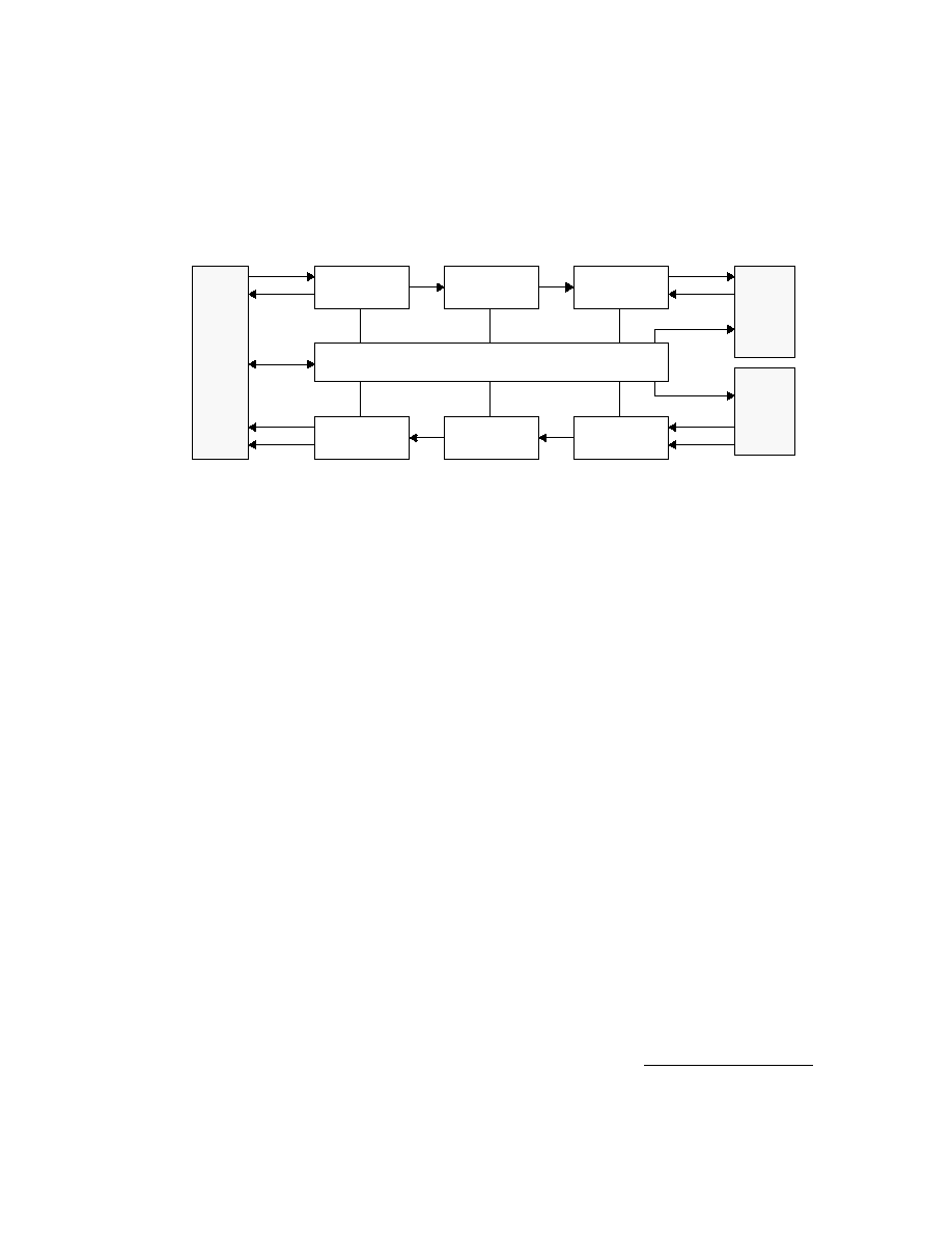
BLOCK DIAGRAM
Figure 1 shows a typical wireless LAN (WLAN) card. The MSM7730 provides a direct connection to a
host interface, processor, radio, shared memory, and configuration EEPROM. The optional addition is a
processor RAM for code storage.
INTERFACE DESCRIPTIONS
The MSM7730 provides the following interfaces:
∑ Processor
∑ Shared RAM
∑ EEPROM
∑ Radio
∑ MODEM
∑ PHY
∑ PCMCIA
These interfaces are explained in the following subsections.
Processor Interface
Most applications require a local processor to handle the higher layers of the IEEE 802.11 protocol. The
host computer typically runs a network device/driver interface specification (NDIS) or open datalink
interface (ODI) driver that communicates to the local processor via shared memory and interrupts. The
local processor performs the higher layers of the IEEE 802.11 MAC protocol while the MSM7730 per-
forms the lower layers of MAC and the PHY under control of the local processor.
Radio
PHY Layer,
Radio Interface
MAC Protocol
Controller
Combined 1 & 2
Mbps Modem
Processor
Interface
Memory
Controller
PCMCIA
Interface
EEPROM
Interface
EEPROM
Shared RAM
(32k~128kx16)
Processor
Processor
RAM
(optional)
MSM7730
Host
Computer
Figure 1. MSM7730 Block Diagram and Typical WLAN Card
≠≠≠≠≠≠≠≠≠≠≠≠≠≠≠≠≠≠≠≠≠≠≠≠≠≠≠≠≠≠≠≠≠≠≠≠≠≠≠≠≠≠≠≠≠≠≠≠≠≠≠≠≠≠≠≠≠≠≠≠≠≠≠≠≠≠≠≠≠≠≠≠≠≠≠≠≠≠≠≠≠≠
s
MSM7730
s
3
Oki Semiconductor
The MSM7730 can be configured to operate with V30HL, V53A, and 80C186 processor types. The proces-
sor configuration is determined from the P_CONF field in the Device Configuration register. The following
table shows how each processor is selected. No external circuitry is required between the processor and
the MSM7730.
In each processor mode, the bus interface module:
∑ Interprets the external bus cycles
∑ Generates the appropriate signals based on the processor mode,
∑ Passes access requests to the host interface module, the shared RAM arbiter, and the baseband
registers.
The module also synchronizes data and control signals to the internal clocks, and interfaces the external
processor to the host interface and processor interrupt control modules.
The 80C186 and V53A processors contain their own clock generator modules and divide-by logic. In
these modes, the MSM7730 generates a clock (X1) at twice the normal operating frequency. The processor
divides this frequency by two (X1/2). Then this clock is used for synchronization of all interface signals.
In V30HL processor mode, the MSM7730 generates the clocks for the internal modules as well as the pro-
cessor. A 16-MHz clock is used during normal operation. This frequency is reduced when the MSM7730
enters either the Hibernate or Smart Hibernate modes. In Hibernate mode the clock frequency is reduced
from 16 MHz to 500 KHz. In Smart Hibernate mode the frequency is reduced to 125 KHz.
Shared RAM Interface
A shared memory interface is provided for the buffering of packets and the storage of processor code and
data. Memory sizes range from 32K words to 128K words in 32K-word increments.
Both 16-bit (word) and 8-bit memory accesses are supported. The MSM7730 and the host computer sup-
port only word accesses to memory. The processor supports both byte and word accesses to memory.
Selection of byte or word transfers occurs on a per-cycle basis and depends on the state of address bit 0
(PD[0]) and the PUBEN signal as shown in the table below.
Selecting the Processor Mode
P_CONF 2:0
Processor Mode
000
Host-only mode. No local processor.
001
V30HL local processor mode.
010
80C186 local processor mode.
011
Reserved
100
V53A local processor mode.
Selecting the Data Transfer Size
PD[0]
PUBEN
Transfer Type
0
0
Word transferred on PD[15:0]
0
1
Even byte transferred on PD[7:0]
1
0
Odd byte transferred on PD[15:8]
1
1
Invalid
s
MSM7730
s
≠≠≠≠≠≠≠≠≠≠≠≠≠≠≠≠≠≠≠≠≠≠≠≠≠≠≠≠≠≠≠≠≠≠≠≠≠≠≠≠≠≠≠≠≠≠≠≠≠≠≠≠≠≠≠≠≠≠≠≠≠≠≠≠≠≠≠≠≠≠≠≠≠≠≠≠≠≠≠≠≠≠≠
4
Oki Semiconductor
For cost-sensitive applications, local processor code may reside in shared memory. However, this may
affect processor because accesses to shared memory may contain wait states.
EEPROM Interface
EEPROM support is provided for nonvolatile storage of host interface configuration (e.g., PCMCIA CIS
table) and WLAN parameters (e.g., local IEEE address, radio parameters). The MSM7730 supports 64-,
128- or 256-byte EEPROM sizes (e.g., 93C46, 93C56, or 93C66 types).
.
The local processor can be used to initialize the EEPROM and control read and writes accesses for pro-
viding card parameter storage.
Following a reset by the host processor, the EEPROM contents are automatically transferred to shared
RAM to provide the configuration information for the host interface. If the device is configured in PC-
card host mode, either 64 or 128 bytes are downloaded to shared RAM to provide the Configuration
Information Structure (CIS). If the device is configured in industry standard architecture (ISA) host
mode, a single word is loaded into an internal register to determine the ISA address space mapping and
interrupt configuration information.
Host Interface (Between Adapter Card and Computer or Laptop)
The 16-bit PCMCIA interface is fully supported by the MSM7730 with no additional logic. Access to
attribute memory (CIS configuration data) and I/O memory (host registers) are provided.
During normal operation, I/O addresses are used to access the baseband controller registers and shared
memory.
Figure 2. EEPROM Connections to MSM7730
EECS
SYNCLK/EESK
SYNDAT/EEDIO
CS
SK
DI
DO
93c46
93c58
94s66
V
V
V
MSM7730
≠≠≠≠≠≠≠≠≠≠≠≠≠≠≠≠≠≠≠≠≠≠≠≠≠≠≠≠≠≠≠≠≠≠≠≠≠≠≠≠≠≠≠≠≠≠≠≠≠≠≠≠≠≠≠≠≠≠≠≠≠≠≠≠≠≠≠≠≠≠≠≠≠≠≠≠≠≠≠≠≠≠
s
MSM7730
s
5
Oki Semiconductor
Radio Interface
The radio interface supports simple, flexible control of the radio and its synthesizer. The control signal
timing is programmable by the processor. Figure 3 shows the connection to a typical radio architecture.
The MSM7730 uses the RXC1 and TXC[1:0] pins to control radio timing. The delay between these signals
is programmable to support different radio designs.
The MSM7730 provides a 24-bit serial programming interface that supports the Seimens PMB2306T and
Philips UMA1020N synthesizers. The synthesizer interface is controlled through the use of an on-chip
synthesizer register.
The MSM7730 provides a hardware controlled serial DAC interface that is not accessible through any
MSM7730 registers. Because the synthesizer and EEPROM share the same clock and data lines, software
is responsible for ensuring that the PHY module is disabled when either of these modules is accessed.
At the start of each transmit packet, one of the four power levels is selected from the on-chip power con-
trol register according to the transmit power level requested by the control word of that packet. During a
receive operation, the serial DAC is used together with an external comparator for RSSI thresholds and
successive approximation measurement. The RSSIA threshold is loaded whenever the receiver is first
powered on. Once the RSSIA threshold is exceeded, the demodulator is accessed and the RSSIB, RSSIC,
and RSSID thresholds are loaded sequentially during each antenna scan. Once antenna scanning has
completed, a successive approximation is started.
Figure 3. Typical FH Radio Interface
RADPWR
RXC1
SLICE
RXD
RSSITH
DACEN
LKDET
SYNCLK
SYNDAT
SYNLEN
IFD[5:0]
TXC1
TXC2
ANT
Diversity Switching
T/R Switch
Disc
-
+
D
CSN
DAC
1LO
2LO
DAC
LNA
PA
Radio
MSM7730
s
MSM7730
s
≠≠≠≠≠≠≠≠≠≠≠≠≠≠≠≠≠≠≠≠≠≠≠≠≠≠≠≠≠≠≠≠≠≠≠≠≠≠≠≠≠≠≠≠≠≠≠≠≠≠≠≠≠≠≠≠≠≠≠≠≠≠≠≠≠≠≠≠≠≠≠≠≠≠≠≠≠≠≠≠≠≠≠
6
Oki Semiconductor
MODEM Interface
The MSM7730 provides Frequency Hopping Physical Layer Convergence Protocol (FH PLCP) framing
and the FH modem as defined by the IEEE 802.11 specification. The radio synthesizer control pins are
used for all modem options. A diagnostic port is provided when the internal modem is used. Several
options are provided by the internal FH modem. The following table shows the pin usage for the various
modem options.
Modulator
The MSM7730 provides an integrated 24-MHz internal digital IF modulator. The modulator generates
ordinary Frequency Shift Keying (CP-FSK) and relies on radio filtering to shape this to Gaussian Fre-
quency Shift Keying (GFSK). Since the radio requires a SAW filter to achieve out-of-band transmit
requirements, this filter can also be used to provide the required in-band frequency response. This pro-
vides for more efficient power consumption because extra digital filtering is not required in the modula-
tor. The modulator is shown in Figure 4.
The modulator supports two modes of modulator operation:
∑ 1-Mbps, 2-ary CP-FSK
∑ 2-Mbps, 4-ary CP-FSK
The modulation scheme for 1-Mbps operation is Gaussian Frequency Shift Keying (GFSK). The modula-
tion scheme for 2-Mbps operation is 4-level GFSK.
Deviations can be set independently for both modes. Modes switch phase continuously in a single clock
cycle.
∑ 1-Mb deviation: 1MDEV = N x 32
6
/4096 Hz
∑ 2-Mb deviation: 2MDEV = N x 3 x 32
6
/4096 Hz
where N = 0.63.
Modem Options and Pin Connections
[1]
1.
All modem signals are synchronized to RCK.
Modem Interface
FH Mbps (Low Cost)
FH 1/2 Mbps (Normal ADC)
FH 1/2 Mbps (Delta ADC)
MSEL
1
2
3
IFD[5:0]
IFD[5:0] to TXIF DAC
IFD[4] carries SLICE on RX
IFD[5:0] to TXIF
DAC and IFD[3:0] from RXADC
IFD[5:0] to TXIF DAC (also used for Delta ADC)
RXD
Baseband RX data from radio
Recovered data (Debug out)
Input from Delta ADC comparator
PHY
RADIO
Input
Processing
Modulator
Ramp
Processing
State Machine
TxData
TxClkEn
IFData
Mode
ModeEn
Figure 4. Modulator Block Diagram
≠≠≠≠≠≠≠≠≠≠≠≠≠≠≠≠≠≠≠≠≠≠≠≠≠≠≠≠≠≠≠≠≠≠≠≠≠≠≠≠≠≠≠≠≠≠≠≠≠≠≠≠≠≠≠≠≠≠≠≠≠≠≠≠≠≠≠≠≠≠≠≠≠≠≠≠≠≠≠≠≠≠
s
MSM7730
s
7
Oki Semiconductor
Digital on/off ramping from 0 to 24 µs of the modulator output power may be added under register con-
trol
Modulator radio requirements are:
∑ 6-bit DAC, clock at 32 MHz (offset binary, 2's complement)
∑ Anti-alias filtering to extract the 24-MHz alias
(24-MHz IF will be -10 dB on 8-MHz fundamental from DAC output)
∑ Gaussian filtering to translate CP-FSK into G-FSK, in accordance with the IEEE 802.11 specification
(SAW filter at 240 MHz, if recommended)
Demodulator
The baseband controller in the MSM7730 incorporates a digital baseband demodulator designed to
demodulate IEEE 802.11 GFSK data packets with 1- and 2-Mbps headers. The demodulator contains the
following features:
∑ 1- and 2-Mbps operation
∑ Two-antenna diversity control
∑ Analog discriminator interface
∑ Flexible clear channel assessment (CCA) options to enhance interference performance
∑ Tunable or adaptive digital filter and data slicers for performance optimization
∑ Clock and carrier tracking for demodulation of long data packets
PHY
RADIO
Input
Processing
State Machine
Figure 5. Demodulator Block Diagram
Slicer
Decode
Pream
UW
Decimating
DLPF
Aperture
Corrector
Detect
Detect
Trans
Detect
Dev
Detect
Carrier
Control
Timing
Control
Data
s
MSM7730
s
≠≠≠≠≠≠≠≠≠≠≠≠≠≠≠≠≠≠≠≠≠≠≠≠≠≠≠≠≠≠≠≠≠≠≠≠≠≠≠≠≠≠≠≠≠≠≠≠≠≠≠≠≠≠≠≠≠≠≠≠≠≠≠≠≠≠≠≠≠≠≠≠≠≠≠≠≠≠≠≠≠≠≠
8
Oki Semiconductor
The MSM7730 supports two modes:
∑ 1-Mbps 2-ary FSK
∑ 2-Mbps 4-ary FSK
The demodulator offers three possible interfaces to a limiter/discriminator radio.
∑ Analog data slicer (1Mbps only)
∑ Post discriminator 4-bit ADC (offset binary)
∑ Post discriminator 1-bit ADC (provisional)
The radio requirements for the demodulator are:
∑ 1 Mb: 20 dB S/N from discriminator 10
-5
BER (802.11 specifies sensitivity of 10
-5
for 80 dBm)
∑ 2 Mb: 30 dB S/N from discriminator 10
-5
BER (802.11specifies sensitivity of 10
-5
for 75 dBm)
∑ Discriminator linearity of ±5% required for specified 2-Mbps operation
∑ 4-bit discriminator-to-ADC ranging, to cover approximately ±360 KHz
∑ Carrier acquisition for analog slicer option within 4 µs, yielding a duty cycle better than 60:40 for a
square wave (demodulation provides signal for carrier lock switch once preamble is detected
∑ RSSI threshold decision within 4 µs of antenna switching
∑ 3-state ADC output during transmit (bus is shared with TxDAC)
PHY Interface
The PHY section of the MSM7730 allows the MAC layers from two different stations to be interconnected
via a 2.4-GHz radio signal. Figure 6 shows a block diagram of the PHY interface.
The PHY provides a slow Frequency Hopping Spread Spectrum (FHSS) radio link at either 1 or 2 Mbps.
FH is performed over a subset of 1-MHz wide channels with a frequency band of 2.400 to 2.497 GHz. The
MSM7730 is not directly in control of the hopping sequence, but rather provides for reprogramming of
the radio channel so that this function can be managed under software control.
The mapping of data between the MAC and the radio link is called the Physical Layer Convergence Pro-
tocol (PLCP). This mapping involves the addition and removal of preamble and header information, as
well as the whitening and dewhitening of packet data. Figure 7 shows a block diagram of the PLCP.
MAC
RADIO
Radio
Control
Demodulator
Modulator
Figure 6. MSM7730 Physical Layer Block Diagram
Modem
Interface
Physical
Layer
Convergence
PHY Interface
≠≠≠≠≠≠≠≠≠≠≠≠≠≠≠≠≠≠≠≠≠≠≠≠≠≠≠≠≠≠≠≠≠≠≠≠≠≠≠≠≠≠≠≠≠≠≠≠≠≠≠≠≠≠≠≠≠≠≠≠≠≠≠≠≠≠≠≠≠≠≠≠≠≠≠≠≠≠≠≠≠≠
s
MSM7730
s
9
Oki Semiconductor
Each frame starts with an 80-bit synchronization sequence or preamble, followed by a 16-bit unique
word or start of frame deliminiter (SFD).
The Physical Data Unit (PDU) is a data-whitened version of the MAC data at either 1 or 2 Mbps. The pre-
amble and header are always transmitted at 1 Mbps. The PDU can be transmitted at either 1 or 2 Mbps.
The PHY is required to perform CCA to determine when to transmit, and for the MAC to control the con-
tention back-off timer.
PCMCIA Interface
The MSM7730 provides a PCMCIA host interface mode designed to permit implementation of PC cards
for use with host computers compatible with the PCMCIA PC card standard (Revision 2.1). The interface
supports 16-bit transfers to maximize overall system throughput. In addition, common memory may be
used to access all control registers. This is useful for low-cost card implementations that do not have a
local processor.
The MSM7730 uses attribute memory to configure the device and card. The device decodes the least-sig-
nificant 9-bits of PC card address space, allowing for an attribute memory size of 512 bytes located at
addresses 0x000 - 0x1FF. The attribute memory stores the PCMCIA registers as well as the card informa-
tion structure (CIS) table data. The PCMCIA standard defines four configuration registers. However,
only the Configuration Option and the Configuration and Status registers are supported, not the Pin Replace-
ment and Socket and Copy registers.
The CIS information data is stored in an off-chip serial EEPROM. When the MSM7730 is reset, the con-
tents of the EEPROM are downloaded to shared RAM. Then the information is mapped to attribute
memory space.
PHY
MOD
Data Whitener
Scrambler
Figure 7. Physical Layer Convergence Protocol Block Diagram
Preamble
De-whitener
De-scrambler
Header
State Machine
Formatting
CRC Check
DEMOD
Add arrows

s
MSM7730
s
≠≠≠≠≠≠≠≠≠≠≠≠≠≠≠≠≠≠≠≠≠≠≠≠≠≠≠≠≠≠≠≠≠≠≠≠≠≠≠≠≠≠≠≠≠≠≠≠≠≠≠≠≠≠≠≠≠≠≠≠≠≠≠≠≠≠≠≠≠≠≠≠≠≠≠≠≠≠≠≠≠≠≠
10
Oki Semiconductor
PIN CONFIGURATION
RA14
1
RA13
2
RA12
3
RA11
4
RA10
5
RA9
6
RA8
7
RA7
8
RA6
9
RA5
10
RA4
11
RA3
12
RA2
13
RA1
14
RA0
15
SCK
16
VDDO
17
VSSO
18
RWRN
19
RCELN
20
RCEHN
21
RD0
22
RD1
23
RD2
24
RD3
25
RD4
26
RD5
27
RD6
28
RD7
29
RD8
30
RD9
31
RD10
32
VDDO
33
VSSO
34
RD11
35
RD12
36
PCLK
108
PRESETN
107
PINTN
106
PCLKOUT
105
PUBE
104
PCSN
103
PREAD
102
PREADYN
101
PD17
100
PD16
99
PD15
98
PD14
97
PD13
96
PD12
95
PD11
94
PD10
93
PD9
92
PD8
91
PD7
90
PD6
89
PD5
88
PD4
87
VSSO
86
VDDO
85
PD3
84
PD2
83
PD1
82
PD0
81
HD3
80
HD11
79
HD4
78
HD12
77
HD5
76
HD13
75
HD6
74
HD14
73
RA15
144
RA16
143
DIAG6
142
DIAG5
141
DIAG4
140
DIAG3
139
DIAG2
138
DIAG1
137
DIAG0
136
RXD
135
VSSO
134
VDDO
133
IFD5
132
IFD4/SLICE
131
IFD3
130
IFD2
129
IFD1
128
IFD0
127
RSSITN
126
ANT
125
RADPWR
124
TXC2
123
TXC1
122
RXC1
121
LKDET
120
SYNLEN
119
EECS
118
SYNDAT/EEDIO
117
SYNCLK/EESK
116
DACEN
115
RCK
114
VSSO
113
VDDO
112
PST0
111
PST1
110
PST2
109
RD13
37
RD14
38
RD15
39
HIOIS16N
40
HD10
41
HD2
42
HD9
43
HD1
44
HD8
45
HD0
46
HA0
47
HA1
48
HREGN
49
HA2
50
HPACKN
51
HA3
52
VDDC
53
VSSC
54
VSSO
55
VDDO
56
HWAITN
57
HA4
58
HRST
59
HA5
60
HA6
61
HA7
62
HIREQN
63
HWEN
64
HIOWRN
65
HA8
66
HIORDN
67
HOEN
68
HCE2N
69
HCE1N
70
HD15
71
HD7
72
Figure 8. 144-Pin Plastic LQFP Pin Assignment

≠≠≠≠≠≠≠≠≠≠≠≠≠≠≠≠≠≠≠≠≠≠≠≠≠≠≠≠≠≠≠≠≠≠≠≠≠≠≠≠≠≠≠≠≠≠≠≠≠≠≠≠≠≠≠≠≠≠≠≠≠≠≠≠≠≠≠≠≠≠≠≠≠≠≠≠≠≠≠≠≠≠
s
MSM7730
s
11
Oki Semiconductor
PIN DESCRIPTIONS
Host Interface Signal Descriptions (PCI and ISA)
Pin Name
Direction
Description
HPACKN
Output
This signal is asserted when the card is selected and can respond to an I/O read cycle at the address on the
address bus.
HIOIS16N
Output
This signal is asserted whenever the access on A[8:0] corresponds to an I/O location which is capable of a 16-
bit access.
HIOWRN
Input
Indicates an I/O write cycle.
HIORDN
Input
Indicates an I/O read cycle.
HIREQN
Output
Active low interrupt request and ready/busy indicator prior to I/O card pin replacement.
HOEN
Input
Output enable signal asserted during memory read operations. Assertion of this signal causes memory data to
be driven onto HD[15:0].
HREGN
Input
Assertion of this signal indicates an access to either attribute memory or I/O space.
HA[8:0]
Input
Least significant 9 bits of the PC-card address bus. All other address bits are ignored.
HCEN[2:1]
Input
Active low card enable signals. HCEN[1] selects even numbered bytes. HCEN[2] selects odd numbered bytes.
HD[15:0]
Bidirectional
Bidirectional data bus. Even numbered bytes appear on HD[7:0]. Odd numbered bytes appear on HD[15:8].
HRST
Input
Active high reset input.
HWAITN
Output
Active low wait output. This signal is asserted if an access is requested that cannot complete immediately.
HWEN
Input
Active low memory write enable input. Indicates a write to either attribute memory or common memory as
determined by the state of the HREGN signal.
HCE1N
Input
Assertion of this signal indicates that a DMA transfer is in progress.
HCE2N
Output
Indicates the ISA shared interrupt status.
Processor Interface Signal Descriptions (V30HL, V53A, and 80C186)
Pin Name
Direction
Description
PD[17:0]
Bidirectional
Bidirectional multiplexed address/data bus driven during the T1 clock state. PD[17:16] are inputs only.
PST[2:0]
Input
Bus status code that indicates the current cycle type. These inputs must be held HIGH when reset is asserted.
PCLK/PCLKOUT
Input/Output
Clock output of the MSM7730 to which all bus interface signals are synchronized. Frequency is 16 MHz during
normal operation but is reduced when in hibernate mode. These two pins must be connected together for
proper operation.
PINTN
Output
This signal is generated by the host and processor interrupt module.
PCSN
Input
Processor chip select.
PREADYN
Output
Active high ready indication from the MSM7730.
PRESETN
Output
This signal is controlled by the host and is asserted based on the state of the PRSTN bit in the H_CTL register.
PUBEN
Input
Upper byte enable. Indicates that a byte of data is to be transferred on PD[15:8].
PREAD
Input
Indicates a read cycle when HIGH, and a write cycle when LOW.

s
MSM7730
s
≠≠≠≠≠≠≠≠≠≠≠≠≠≠≠≠≠≠≠≠≠≠≠≠≠≠≠≠≠≠≠≠≠≠≠≠≠≠≠≠≠≠≠≠≠≠≠≠≠≠≠≠≠≠≠≠≠≠≠≠≠≠≠≠≠≠≠≠≠≠≠≠≠≠≠≠≠≠≠≠≠≠≠
12
Oki Semiconductor
Shared RAM Interface Signal Descriptions
Pin Name
Direction
Description
RA[16:0]
Output
The RAM address is provided by these pins. A maximum address size of 128K words is supported.
RD[15:0]
Bidirectional
The RAM data is provided on these pins. Word or byte operations are supported. When the shared memory is
not in use, the data bus is output to prevent a floating data bus consuming power.
RCELN
Output
When asserted, a low byte (or word) shared RAM cycle is active.
RCEHN
Output
When asserted, a high byte (or word) shared RAM cycle is active.
RWRN
Output
When asserted, a write cycle is required. When deasserted a read cycle is required. This signal remains valid
before and while RCELN and RCEHN are asserted.
EEPROM Interface Signal Descriptions
Pin Name
Direction
Description
EEDIO
Bidirectional
This is a bidirectional data signal for the EEPROM connected directly to data in (DI) of the EEPROM, and to data
out (DO) via a resistor (see EEPROM application notes and
Figure 2).
EECS
Output
This signal is connected to CS of the EEPROM to provide the chip select.
EESK
Output
This signal is connected to SK of the EEPROM to provide the clock. The clock rate is RCK divided by 64 (250
kHz with RCK at 16 MHz).
Radio Interface Signal Descriptions
Pin Name
Direction
Description
RXC1
Open-
collector/drain
Output
When asserted reception is enabled, RXC1 is always asserted during reception. This signal is programmable
to be open-collector (active low) or open-drain (active high).
TXC, TXC2
Open-
collector/drain
Output
When asserted transmission is enabled, both signals are programmable to be open-collector (active low) or
open-drain (active high). Transmit is only activated following a receive (where Clear Channel Assessment is
performed). The timing of TXC1 and TXC2 at the start of a transmit is programmable from the deassertion of
RXC1. RXC2 is typically used for TX Power Amplifier switching, and its assertion depends on the power control
mode selected in the MSM7730.
RADPWR
Open-
collector/drain
output
This pin is asserted to power up the radio circuitry (i.e.,local oscillators) for reception. The pin is programmable
to be open-collector (active low) or open-drain (active high).
ANT
Open-collector
output
This pin selects one of two antennas for transmission or reception.
SLICE
Open-
collector/drain
output
This control pin determines the response time constant of an analog data slicer when using the internal modem
with an analog data slicer circuit (options MSEL-0 or 1). This pin is programmable to be open-collector (active
low) or open-drain (active high). The pin is asserted when CCA has determined a valid IEEE 802.11 GH signal
(preamble is detected).
SYNCLK,
SYNDAT,
SYNLEN
Open collector
These signals provide the interface to the radio synthesizer to select the transmit/receive carrier. Many
synthesizers are supported by a flexible architecture. The data is output on SYNDAT ready for the rising edge
of SYNCLK. SYNLEN is asserted during the programming, and the data is latched on the rising edge of
SYNCLEN. SYNCLK is clocked at RCK divided by 2.
SYNCLK and SYNDAT also are used to program a serial DAC used for TX power control, CCA threshold and
RSSI measurement (see below). The synthesizer is programmed when the radio is idle. The RSSI and CCA
threshold DAC is used at the start of receiving a packet. The TX power DAC is programmed at the start of
transmitting packet.
The radio provides indication of being in lock with LKDET. This input is active high or low (programmable),
pulse sensitive, and latched so that both pulsed and steady out-of-lock signals are recognized. Glitches shorter
than 2 RCK periods are ignored. Transmission is prevented when the synthesizer is out-of-lock
LKDET
Input

≠≠≠≠≠≠≠≠≠≠≠≠≠≠≠≠≠≠≠≠≠≠≠≠≠≠≠≠≠≠≠≠≠≠≠≠≠≠≠≠≠≠≠≠≠≠≠≠≠≠≠≠≠≠≠≠≠≠≠≠≠≠≠≠≠≠≠≠≠≠≠≠≠≠≠≠≠≠≠≠≠≠
s
MSM7730
s
13
Oki Semiconductor
DACEN
Open-collector
For TX power control, CCA threshold and RSSI measurement, data also is clocked into a serial DAC (10/12 bit
type; e.g., MAX515/MAX539) using the SYNCLK and SYNDAT lines as described above, except that DACEN is
asserted during the programming, and the data is latched on the rising edge of DACEN.
RSSITH is an input from a threshold comparison of the analog RSSI signal from the radio with the DAC output.
It is high when the received signal exceeds the programmed threshold. This performs two purposes:
A minimum threshold of RSSI can be set before enabling the demodulator for CCA to reduce power.
Once a valid receive signal is determined (CCA invalid), the RSSI can be measured with the external
comparator/DAC and a SAR within the MSM7730. The RSSI measurement is performed for internal and
external modem options when CCA is determined.
The same DAC can be used for both TX power control, RSSI threshold and RSSI measurement.
RSSITN
Input
RCK
Output
A clock to the radio is provided on this pin. The clock is derived from SCK when RADPWR is asserted, with
fixed division ratio of one or two (selected by post-reset configuration SCK_CONF). RCK is typically 16 MHz
for the radio synthesizer reference.
RXD
Input
The function of this pin depends on the state of the MSEL[3:0] field in the PHY_CONFIG register.
Modem Interface Signal Descriptions
Pin Name
Direction
Description
IFD[5:0]
Bidirectional
If MSEL = 1 (low cost for 1-Mbps modem), IFD[5:0] are used to drive a 6-bit DAC at 32 MHz to provide the
modulated transmit IF signal at 24 MHz. They are set to the DAC mid-value during receive. It is anticipated that
a resistor ladder DAC will be used.
If MSEL = 2,3, (1/2-Mbps modem), IFD[5:0] are used to drive a 6-bit DAC at 32 MHz to provide the modulated
transmit IF signal at 24 MHz.
If MSEL = 2 (1/- Mbps modem, normal ADC) a 4-bit ADC (e.g., CA3304 type) provides digitized demodulated
data at 16 MHz as input to the baseband controller on pins IFD[3:0] during receive. The ADC outputs must only
be enabled during receive (e.g. by connecting RXC1 to the ADC output enable pin).
If MSEL = 3 (1/2-Mbps modem, delta ADC), a comparator is used to compare the value of the transmit IF DAC
output to the receive demodulated signal, performing a tracing delta ADC function. The same 6-bit DAC (but at
16 MHz) is used on IFD[5:0] as during transmit, and the comparator input is connected to the RXD pin.
RXD
Input
When MSEL = 1 (low-cost 1-Mbps modem), the RXD pin is used for baseband data input from a radio which
has a built-in analog data slicer. The MSM7730 has a clock recovery circuitry to synchronize to the incoming
data. The recovered clock is output on a diagnostic pin for test purposes.
When MSEL = 3 (1/2-Mbps modem, delta ADC), the delta comparator is input on this pin. The recovered clock
from the demodulator is output on a diagnostic pin for test purposes.
DIAG[6:0]
Output
Various signals are provided on these pins as diagnostic aids. The registers PHY_CTL[DIAG] and
DEM_CTL0[DTST] select what signals are provided on these pins.
General Signal Descriptions
Pin Name
Direction
Description
SCK
Input
The system clock to the MSM7730 is provided by this pin. The clock must always be active (i.e., when reset is
asserted). The WLAN card operates synchronously to this clock.
The MSM7730 and radio operate at SCK/2. The internal modem operates at SCK (32 MHz).
The processor operates from a division of SCK (divide by 1 to divide by 8) depending on a register (GLOB_CTL,
see Programmers Reference) in the MSM7730. This signal is output as PCK.
VSSC
Ground
These pins serve as ground for the core logic.
VSSO
Power
This pin serves as ground for the I/O pads.
VDDC
Power
This pin serves as power to the core at 3-V nominal.
VDDO
Power
This pin serves as power to I/O pads and can either be 3 V or 5 V nominal.
Radio Interface Signal Descriptions (Continued)
Pin Name
Direction
Description

s
MSM7730
s
≠≠≠≠≠≠≠≠≠≠≠≠≠≠≠≠≠≠≠≠≠≠≠≠≠≠≠≠≠≠≠≠≠≠≠≠≠≠≠≠≠≠≠≠≠≠≠≠≠≠≠≠≠≠≠≠≠≠≠≠≠≠≠≠≠≠≠≠≠≠≠≠≠≠≠≠≠≠≠≠≠≠≠
14
Oki Semiconductor
MSM7730 REGISTER MAP
The following table lists the registers in the MSM7730.
MSM7730 Register Map
Byte
Offset
Register
Group
Width
(bits)
Register Name
Description
0x00
Configura-
tion
8
Device Configuration
Stores serial EEPROM size and sets host interface and processor interface
modes.
0x10
PCMCIA
8
Configuration Option
Stores interrupt, reset, and configuration index information.
0x12
8
Configuration and Status
Stores general cycle status information, including interrupts and power-
down.
0x00
ISA Host
16
Host Control (H_CTL)
Contains ISA reset, host interface and processor interface interrupt
information
0x02
16
Host Address (H_ADDR)
Contains the address in shared memory to be accessed by the H_DATA
register.
0x04
16
Host Data (H_DATA)
Stores host data information.
0x00
Global Con-
trol
16
Version Number
Contains the MSM7730 version number (0xC3). This register is read-only.
0x02
16
Global Control
Contains mapping information for baseband control registers and MAC/PHY
enables.
0x08
16
Processor Interrupt Control
Contains host interrupt, processor interrupt, and interrupt enable information.
0x0C
EEPROM
16
EEPROM Data
This register is a buffer that contains data being transferred to and from the
EEPROM.
0x0E
16
EEPROM Address Control
Contains EEPROM enable and cycle type information.
0x10
PHY/Radio
16
PHY Configuration
Contains Modem and PHY revision information as well as transmit and
receive status. The 3-bit MSEL field defines the type of modem operation..
0x12
16
Synthesizer Program
Contains the least-significant 16 bits of the 32 bits used for synthesizer
programming. This register is used in conjunction with the other SYN register
located at 0x14.
0x14
16
Synthesizer Program
Contains the most-significant 16 bits of the 32 bit s used for synthesizer
programming. This register is used in conjunction with the other SYN register
located at 0x12.
0x16
16
Radio Control (RAD_CTL)
Contains radio configuration and transmit and receive status information.
0x18
16
Radio Delay (RAD_DLYS)
Contains programmable delay parameters between the TXC[1:0] and RXC1
signals.
0x1A
16
Radio Power (RAD_PWR)
Determines when the TXC2 signal is asserted if the power control word is
selected. Two control bits in the PHY control word of a transmit packet
determine which one of four 8-bit values is used. This register is used in
conjunction with the other PAD_PWR register located at 0x1C.
0x1C
16
Radio Power (RAD_PWR)
Determines when the TXC2 signal is asserted if the power control word is
selected. Two control bits in the PHY control word of a transmit packet
determine which one of four 8-bit values is used. This register is used in
conjunction with the other PAD_PWR register located at 0x1A.

≠≠≠≠≠≠≠≠≠≠≠≠≠≠≠≠≠≠≠≠≠≠≠≠≠≠≠≠≠≠≠≠≠≠≠≠≠≠≠≠≠≠≠≠≠≠≠≠≠≠≠≠≠≠≠≠≠≠≠≠≠≠≠≠≠≠≠≠≠≠≠≠≠≠≠≠≠≠≠≠≠≠
s
MSM7730
s
15
Oki Semiconductor
0x1E
Modem
16
RSSIAB
Contains two 6-bit fields: RSSIA and RSSIB. RSSIA is set to correspond to -
65 dB T the radio input. RSSIB is set to correspond to -85 dB T the radio input.
0x20
16
PHY Control (PHY_CTL)
Contains PHY transmit, receive, and Clear Channel Assessment (CCA) status.
0x22
16
User I/O port (internal)
The internal port is selected when the MSEL field in the PHY Configuration
registers equals a value between 0 and 3. The bit descriptions are different
depending on whether this registers is configured for internal or external use
(see next register entry). In the internal mode, the two 6-bit fields configure
each bit of the user I/O port as input or output, and whether values can be read
from or written to this register.
16
User I/O Port (external)
The external port is selected when the MSEL field in the PHY Configuration
registers equals a value between 4 and 7. The bit descriptions are different
depending on whether this registers is configured for internal or external use
(see above register entry). One 6-bit field contains the number of clock
periods from TXDRDY or RXDRDY assertion. The other 6-bit field contains
the number of RXCLK periods from the length field to the start of the PDU
packet.
0x26
16
RSSICD
Contains two 6-bit fields: RSSIC and RSSID. RSSIC corresponds to -80 dBm
at the radio input. RSSID corresponds to -75 dBm at the radio input.
0x28
16
Modem Control 0
Contains two 6-bit fields that set the 1- and 2-Mbps inner symbol modulation
index.
0x2A
16
Modem Control 1
Contains settings for parameters such as integration time for slow carrier
tracking group, antenna scan delay, ramp-up, and ramp-down sequences.
0x2C
16
Demodulator Control 0
Contains demodulator control word settings.
0x2E
16
Demodulator Control 1
Contains noise threshold and jamming counter information.
0x30
MAC Controll
16
Version Number
Contains the MSM7730 MAC version number (0x83).
0x32
16
Buffer Control
Contains the size and address of the receive circular buffer in shared memory.
0x34
16
Rx In Pointer
Contains a word offset from the start of the receive circular buffer in shared
memory. The offset indicates the location of the address where the next word
to be received will be stored.
0x36
16
Rx Out Pointer
Contains a word offset from the start of the receive circular buffer in shared
memory. The offset indicates the first word in the buffer that is available for
use by MAC hardware.
0x40
16
Power Down Control
Contains Hibernate mode request and wakeup information.
0x44
16
MAC Control
Contains filtering mode parameters as well as transmit, receive, PHY, and
modem enable information.
0x46
16
Tx Pointer
Contains the word offset from the start of the transmit pointer table.
0x48
16
Interrupt Enable
Enables interrupts based on the event type.
0x4A
16
Interrupt Acknowledge
This register has the exact same format as the Interrupt Enable register.
Setting a bit in this registers clears the corresponding bit in the Interrupt
Enable register.
0x4C
16
Interrupt Status
This register has the exact same format as the Interrupt Enable register but is
read-only. This register is written by hardware.
0x4E
16
Sequencer Status
Indicates current sequencer activity. Most bits are written by hardware and
are read-only. However, a global clear bit allows for all of the read-only bits to
be cleared at the same time.
MSM7730 Register Map (Continued)
Byte
Offset
Register
Group
Width
(bits)
Register Name
Description

s
MSM7730
s
≠≠≠≠≠≠≠≠≠≠≠≠≠≠≠≠≠≠≠≠≠≠≠≠≠≠≠≠≠≠≠≠≠≠≠≠≠≠≠≠≠≠≠≠≠≠≠≠≠≠≠≠≠≠≠≠≠≠≠≠≠≠≠≠≠≠≠≠≠≠≠≠≠≠≠≠≠≠≠≠≠≠≠
16
Oki Semiconductor
0x50
MAC Control
16
TSF Timer
This register works in conjunction with the register at address 0x52 to
construct a 32-bit microsecond timer used for time stamps in received frames
and beacon transmissions.
0x52
16
TSF Timer
This register works in conjunction with the register at address 0x50 to
construct a 32-bit microsecond timer used for time stamps in received frames
and beacon transmissions.
0x58
16
TSF Comparator 1
This register contains the least-significant 16 bits of a 24-bit TSF timer value.
This register works in conjunction with the register at address 0x5A. The 16
bits of the TSF Comparator 1 register and the 8-bits of the TSF Comparator 2
register comprise the 24-bit TSF comparator value.
0x5A
16
TSF Comparator 2
This register contains the most-significant 8 bits of a 24-bit TSF timer value.
This register works in conjunction with the register at address 0x58. The 16
bits of the TSF Comparator 1 register and the 8-bits of the TSF Comparator 2
register comprise the 24-bit TSF comparator value. This 8-bit value is
contained in the lower 8 bits of this register. The upper 8 bits are reserved.
0x60
16
Add TSF Time
Hardware uses the lower 10 bits of this register to determine the length of
time that the TSF timer is disabled. This value can be modified by software.
0x64
16
NAV Timer
This 16-bit register contains a 1-µs resolution timer that maintains the virtual
carrier sense mechanism. The timer is automatically loaded by the MAC but
can be modified by software.
0x66
16
Backoff Timer
This register is loaded automatically by the MAC from transmit frame header
structures. If a backoff condition occurs, the counter begins decrementing
until it reaches zero.
0x68
16
Response Timer
Contains a timeout value, in increments of 32 µs, after which the MAC aborts
the transmit frame if it does not receive an acknowledgment.
0x6A
16
Tick Timer
Sets the interval time in milliseconds at which interrupts are generated.
0x6C
16
Timer Control
Contains enable and status information for each of the timers in the MAC
control register group.
0x6E
16
Slot Time
Contains the value used to determine the length of slots required for random
backoff.
MSM7730 Register Map (Continued)
Byte
Offset
Register
Group
Width
(bits)
Register Name
Description

Oki Semiconductor
The information contained herein can change without notice owing to product and/or technical improvements.
Please make sure before using the product that the information you are referring to is up-to-date.
The outline of action and examples of application circuits described herein have been chosen as an explanation of the standard action
and performance of the product. When you actually plan to use the product, please ensure that the outside conditions are reflected in
the actual circuit and assembly designs.
Oki assumes no responsibility or liability whatsoever for any failure or unusual or unexpected operation resulting from misuse, neglect,
improper installation, repair, alteration or accident, improper handling, or unusual physical or electrical stress including, but not limited
to, exposure to parameters outside the specified maximum ratings or operation outside the specified operating range.
Neither indemnity against nor license of a third party's industrial and intellectual property right,etc.is granted by us in connection with
the use of product and/or the information and drawings contained herein. No responsibility is assumed by us for any infringement of a
third party's right which may result from the use thereof.
When designing your product, please use our product below the specified maximum ratings and within the specified operating ranges,
including but not limited to operating voltage, power dissipation, and operating temperature.
The products listed in this document are intended for use in general electronics equipment for commercial applications (e.g.,office
automation, communication equipment, measurement equipment, consumer electronics, etc.).These products are not authorized for
use in any system or application that requires special or enhanced quality and reliability characteristics nor in any system or application
where the failure of such system or application may result in the loss or damage of property or death or injury to humans. Such
applications include, but are not limited to: traffic control, automotive, safety, aerospace, nuclear power control, and medical, including
life support and maintenance.
Certain parts in this document may need governmental approval before they can be exported to certain countries. The purchaser
assumes the responsibility of determining the legality of export of these parts and will take appropriate and necessary steps, at their
own expense, for export to another country.
Copyright 1998 Oki Semiconductor
Oki Semiconductor reserves the right to make changes in specifications at anytime and without notice. This information furnished by
Oki Semiconductor in this publication is believed to be accurate and reliable. However, no responsibility is assumed by Oki
Semiconductor for its use; nor for any infringements of patents or other rights of third parties resulting from its use. No license is
granted under any patents or patent rights of Oki.

Northwest Area
785 N. Mary Avenue
Sunnyvale, CA 94086
Tel: 408/720-8940
Fax: 408/720-8965
Southwest Area
2302 Martin Street
Suite 250
Irvine, CA 92715
Tel: 714/752-1843
Fax: 714/752-2423
North Central Area
17177 N. Laurel Park Drive
Suite 433
Livonia, MI 48152
Tel: 313/464-7200
Fax: 313/464-1724
South Central Area
2007 N. Collins Blvd.
Suite 303
Richardson, TX 75080
Tel: 972/690-6868
Fax: 972/690-8233
North East Area
138 River Road
Shattuck Office Center
Andover, MA 01810
Tel: 978/688-8687
Fax: 978/688-8896
Southeast Area
1590 Adamson Parkway
Suite 220
Morrow, GA 30260
Tel: 770/960-9660
Fax: 770/960-9682
Oki R
EGIONAL
S
ALES
O
FFICES
Corporate Headquarters
785 N. Mary Avenue
Sunnyvale, CA 94086-2909
Tel: 408/720-1900
Fax: 408/720-1918
Oki Stock No:
Oki FaxBack Service:
Call toll free 1-800-OKI-6994
Oki WebSite:
http://www.okisemi.com
320027-001