1/37
¡ Semiconductor
MSM80C86A-10RS/GS/JS
GENERAL DESCRIPTION
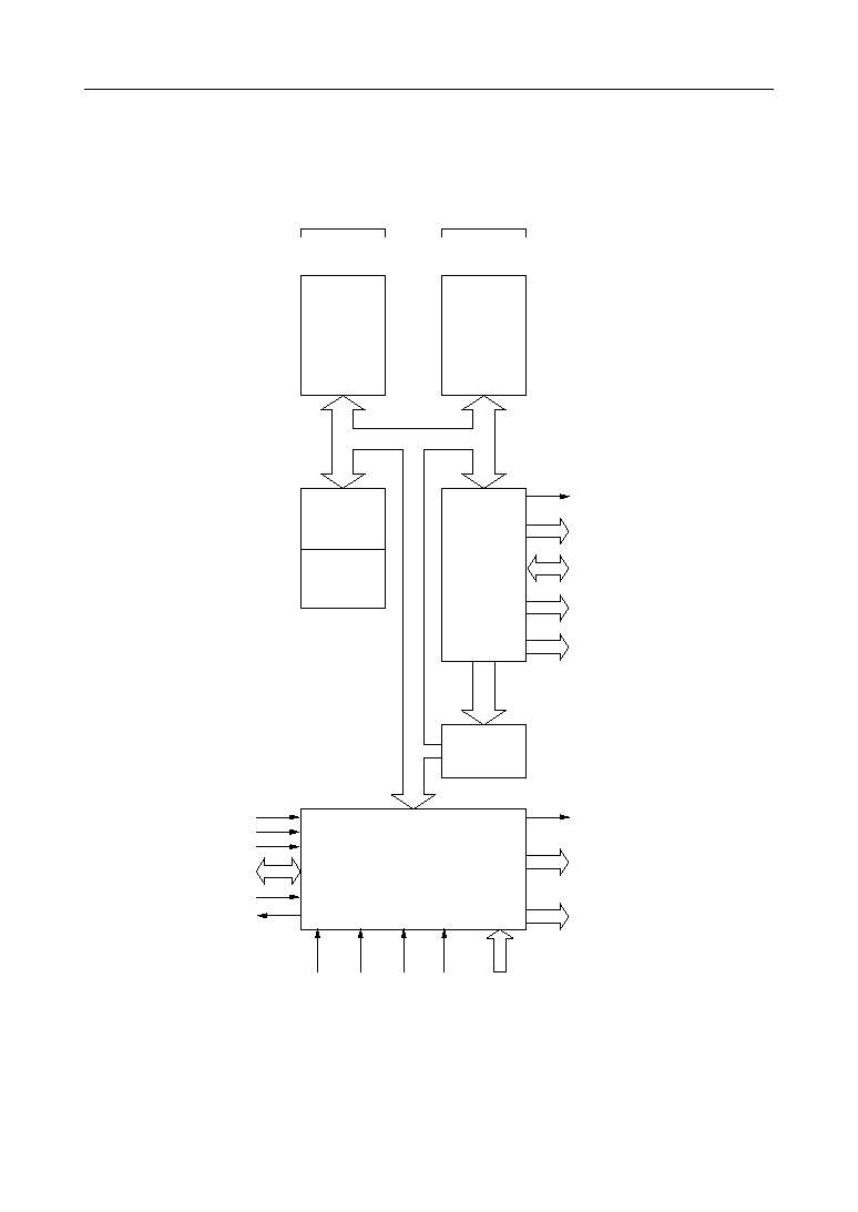
The MSM80C86A-10 is complete 16-bit CPUs implemented in Silicon Gate CMOS technology.
They are designed with same processing speed as the NMOS 8086-1 but have considerably less
power consumption. It is directly compatible with MSM80C88A-10 software and MSM80C85AH
hardware and peripherals.
FEATURES
· 1 Mbyte Direct Addressable Memory Space
· Internal 14-word by 16-bit Register Set
· 24-Operand Addressing Modes
· Bit, Byte, Word and String Operations
· 8 and 16-bit Signed and Unsigned Arithmetic Operation
· From DC to 10 MHz Clock Rate (Note)
· Low Power Dissipation 10 mA/MHz
· Bus Hold Circuitry Eliminated Pull-up Resistors
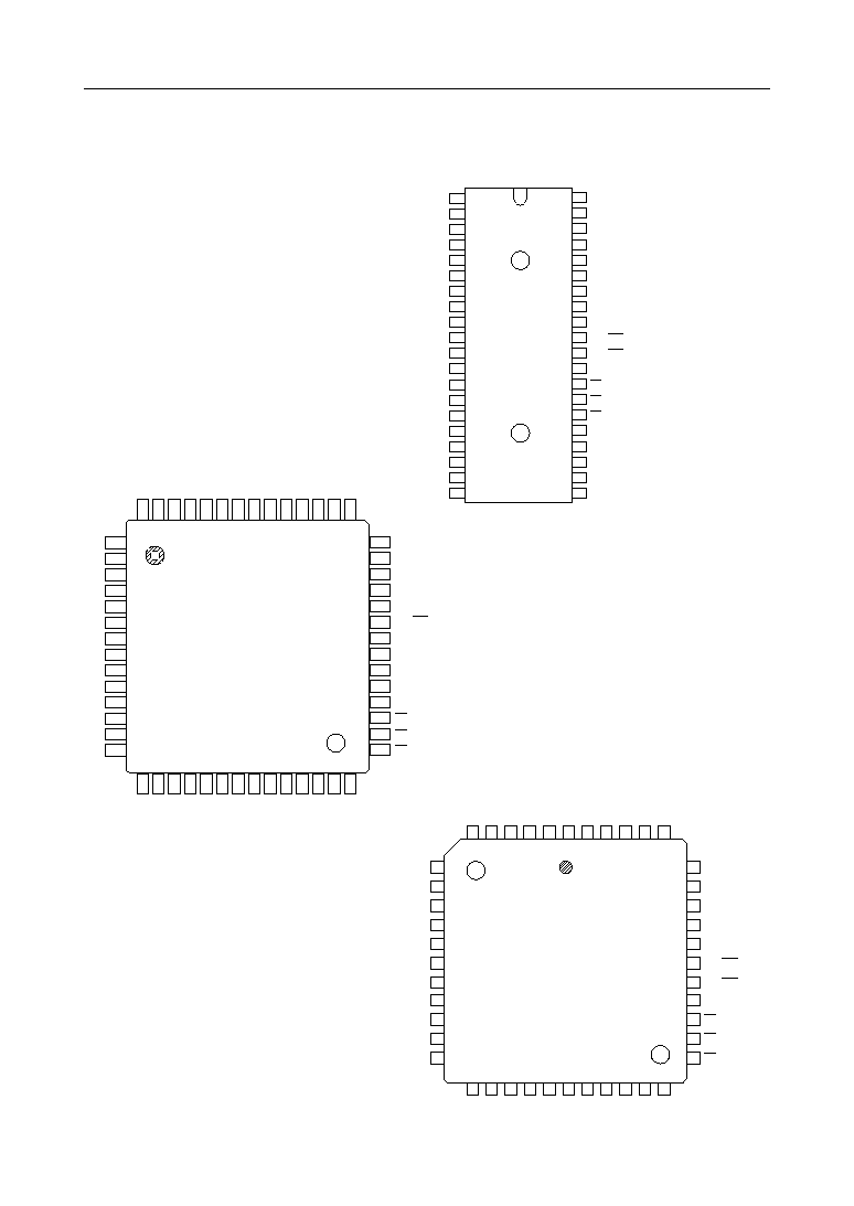
· 40-pin Plastic DIP (DIP40-P-600-2.54): (Product name: MSM80C86A-10RS)
· 44-pin Plastic QFJ (QFJ44-P-S650-1.27): (Product name: MSM80C86A-10JS)
· 56-pin Plastic QFP (QFP56-P-1519-1.00-K): (Product name: MSM80C86A-10GS-K)
(Note) 10 MHz Spec is not compatible with Intel 8086-1 Spec.
¡ Semiconductor
MSM80C86A-10RS/GS/JS
16-Bit CMOS MICROPROCESSOR
E2O0010-27-X2
This version: Jan. 1998
Previous version: Aug. 1996
5/37
¡ Semiconductor
MSM80C86A-10RS/GS/JS
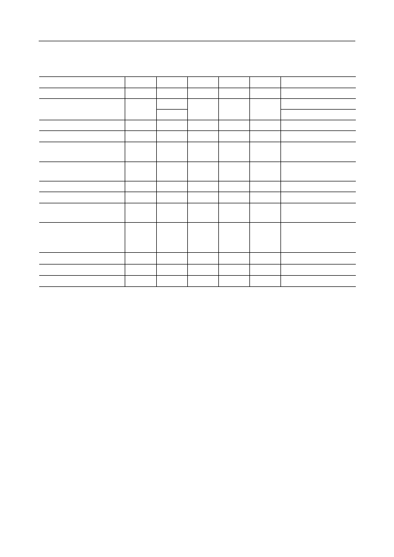
DC CHARACTERISTICS
Max.
"L" Output Voltage
V
OL
0.4
V
"H" Output Voltage
V
OH
--
--
V
Parameter
Unit
Symbol
Min.
--
3.0
V
CC
0.4
I
OL
= 2.5 mA
I
OH
= 2.5 mA
I
OH
= 100 mA
Conditions
Input Leak Current
I
LI
+1.0
mA
Output Leak Current
I
LO
+10
mA
1.0
10
0 £ V
IN
£ V
CC
V
O
= V
CC
or GND
Typ.
Input Leakage Current
(Bus Hold Low)
I
BHL
400
mA
50
V
IN
= 0.8 V
*3
Input Leakage Current
(Bus Hold High)
I
BHH
400
mA
50
V
IN
= 3.0 V
*4
Bus Hold Low Overdrive
I
BHLO
600
mA
--
*5
Bus Hold High Overdrive
I
BHHO
600
mA
--
*6
Operating Power
Supply Current
I
CC
10
Standby Power
Supply Current
I
CCS
500
--
--
V
IL
= GND
V
IH
= V
CC
V
CC
= 5.5 V
Outputs Unloaded
V
IN
= V
CC
or GND
mA/MHz
mA
Input Capacitance
C
IN
10
pF
Output Capacitance
C
OUT
15
pF
--
--
I/O Capacitance
C
I/O
20
pF
*7
*7
*7
--
--
--
--
--
--
--
--
--
--
--
--
--
(V
CC
= 4.5 to 5.5 V, Ta = 40°C to +85°C)
*3 Test condition is to lower V
IN
to GND and then raise V
IN
to 0.8 V on pins 2-16, and 35-39.
*4 Test condition is to raise V
IN
to V
CC
and then lower V
IN
to 3.0 V on pins 2-16, 26-32, and 34-
39.
*5 An external driver must source at least I
BHLO
to switch this node from LOW to HIGH.
*6 An external driver must sink at least I
BHHO
to switch this node from HIGH to LOW.
*7 Test Conditions: a) Freq = 1 MHz.
b) Unmeasured Pins at GND.
c) V
IN
at 5.0 V or GND.