 | –≠–ª–µ–∫—Ç—Ä–æ–Ω–Ω—ã–π –∫–æ–º–ø–æ–Ω–µ–Ω—Ç: MSM82C54 | –°–∫–∞—á–∞—Ç—å:  PDF PDF  ZIP ZIP |

1/23
° Semiconductor
MSM82C54-2RS/GS/JS
GENERAL DESCRIPTION
The MSM82C54-2RS/GS/JS is a programmable universal timer designed for use in
microcomputer systems. Based on silicon gate CMOS technology, it requires a standby current
of only 10 mA (max.) when the chip is in the non-selected state. And during timer operation, the
power consumption is still very low with only 10mA (max.) of current required.
It consists of three independent counters, and can count up to a maximum of 10 MHz. The timer
features six different counter modes, and binary count/BCD count functions. Count values can
be set in byte or word units, and all functions are freely programmable.
FEATURES
∑ Maximum operating frequency of 10 MHz (V
CC
=5 V)
∑ High speed and low power consumption achieved by silicon gate CMOS technology
∑ Completely static operation
∑ Three independent 16-bit down-counters
∑ Status Read Back Command
∑ Six counter modes available for each counter
∑ Binary and decimal counting possible
∑ 24-pin Plastic DIP (DIP24-P-600-2.54): (Product name: MSM82C54-2RS)
∑ 28-pin Plastic QFJ (QFJ28-P-S450-1.27): (Product name: MSM82C54-2JS)
∑ 32-pin Plastic SSOP (SSOP32-P-430-1.00-K): (Product name: MSM82C54-2GS-K)
° Semiconductor
MSM82C54-2RS/GS/JS
CMOS PROGRAMMABLE INTERVAL TIMER
E2O0019-27-X2
This version: Jan. 1998
Previous version: Aug. 1996
2/23
° Semiconductor
MSM82C54-2RS/GS/JS
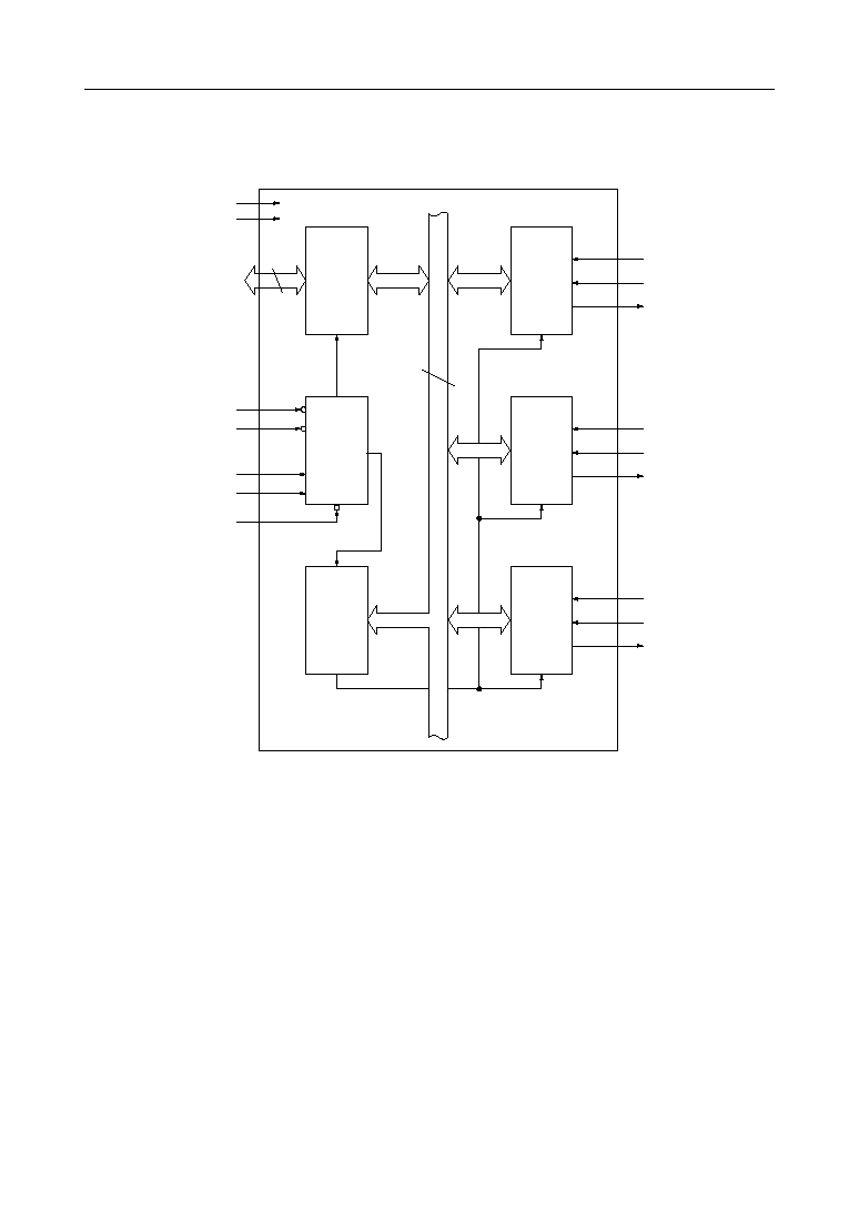
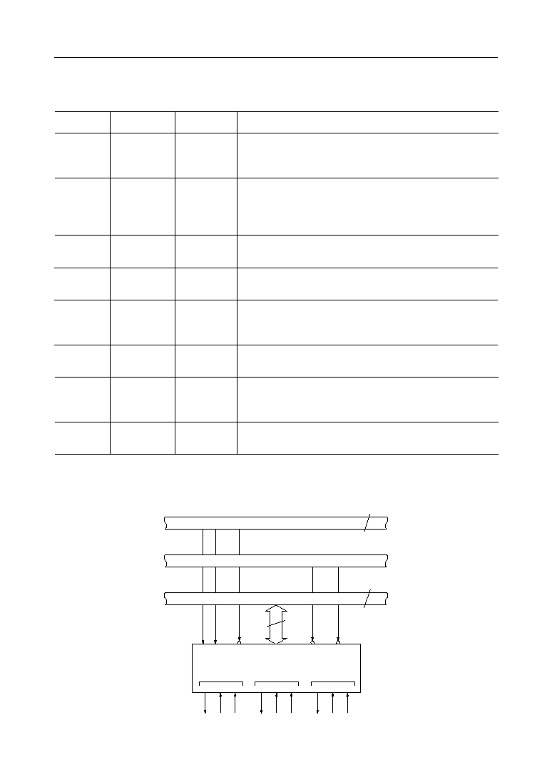
FUNCTIONAL BLOCK DIAGRAM
Data
Bus
Buffer
8
D
7
- D
0
Counter
#0
CLK
0
GATE
0
OUT
0
Read/
Write
Logic
Counter
#1
CLK
1
GATE
1
OUT
1
V
CC
GND
WR
RD
A
0
A
1
CS
Control
Word
Register
Counter
#2
CLK
2
GATE
2
OUT
2
Internal Bus
8

3/23
° Semiconductor
MSM82C54-2RS/GS/JS
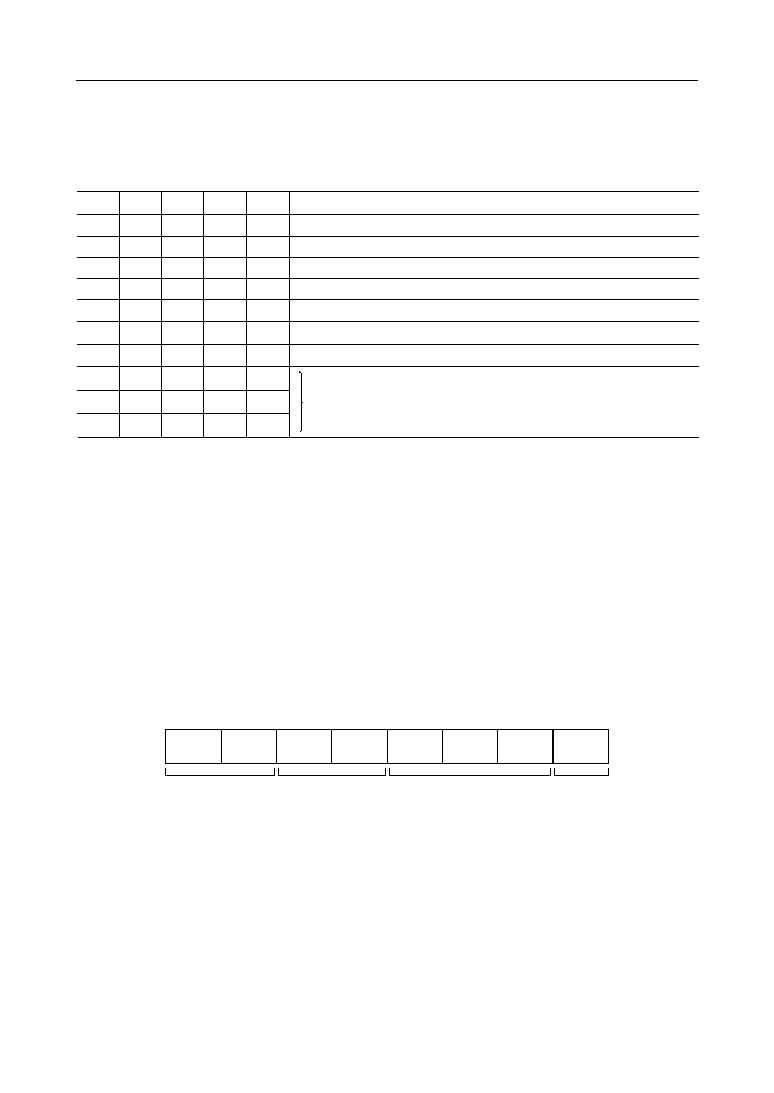
PIN CONFIGURATION (TOP VIEW)
1
2
3
4
5
6
7
8
9
10
11
12
24
23
22
21
20
19
18
17
16
15
14
13
D
7
D
6
D
5
D
4
D
3
D
2
D
1
D
0
V
cc
WR
RD
CS
A
1
A
0
CLK
2
OUT
2
CLK
0
OUT
0
GATE
0
GND
GATE
2
CLK
1
GATE
1
OUT
1
24 pin Plastic DIP
16
15
14
13
NC
D
7
D
6
D
5
NC
D
4
D
3
D
2
D
1
D
0
CLK
0
NC
OUT
0
GATE
0
GND
NC
NC
V
cc
WR
RD
NC
CS
A
1
A
0
CLK
2
OUT
2
GATE
2
NC
CLK
1
GATE
1
OUT
1
NC
1
2
3
4
5
6
7
8
9
10
11
12
32 pin Plastic SSOP
24
23
22
21
20
19
18
29
30
31
32
28
27
26
25
17
25
24
23
22
21
20
19
NC
CS
A
1
A
0
CLK
2
OUT
2
GATE
2
D
4
D
3
D
2
D
1
D
0
CLK
0
NC
12
13
14
15
16
17
18
OUT
0
GATE
0
GND
NC
OUT
1
GATE
1
CLK
1
4
3
2
1
28
27
26
D
5
D
6
D
7
NC
V
CC
WR
RD
5
6
7
8
9
10
11
28 pin Plastic QFJ
(NC denotes "not connected".)
4/23
° Semiconductor
MSM82C54-2RS/GS/JS
ABSOLUTE MAXIMUM RATING
≠55 to +150
MSM82C54-2RS
Power Supply Voltage
V
CC
≠0.5 to +7
V
Input Voltage
V
IN
≠0.5 to V
CC
+0.5
V
Output Voltage
V
OUT
≠0.5 to V
CC
+0.5
V
Storage Temperature
T
STG
∞C
Power Dissipation
P
D
0.7
W
Parameter
Unit
Symbol
With
respect to GND
--
Ta = 25∞C
Condition
Rating
MSM82C54-2GS MSM82C54-2JS
0.9
0.9
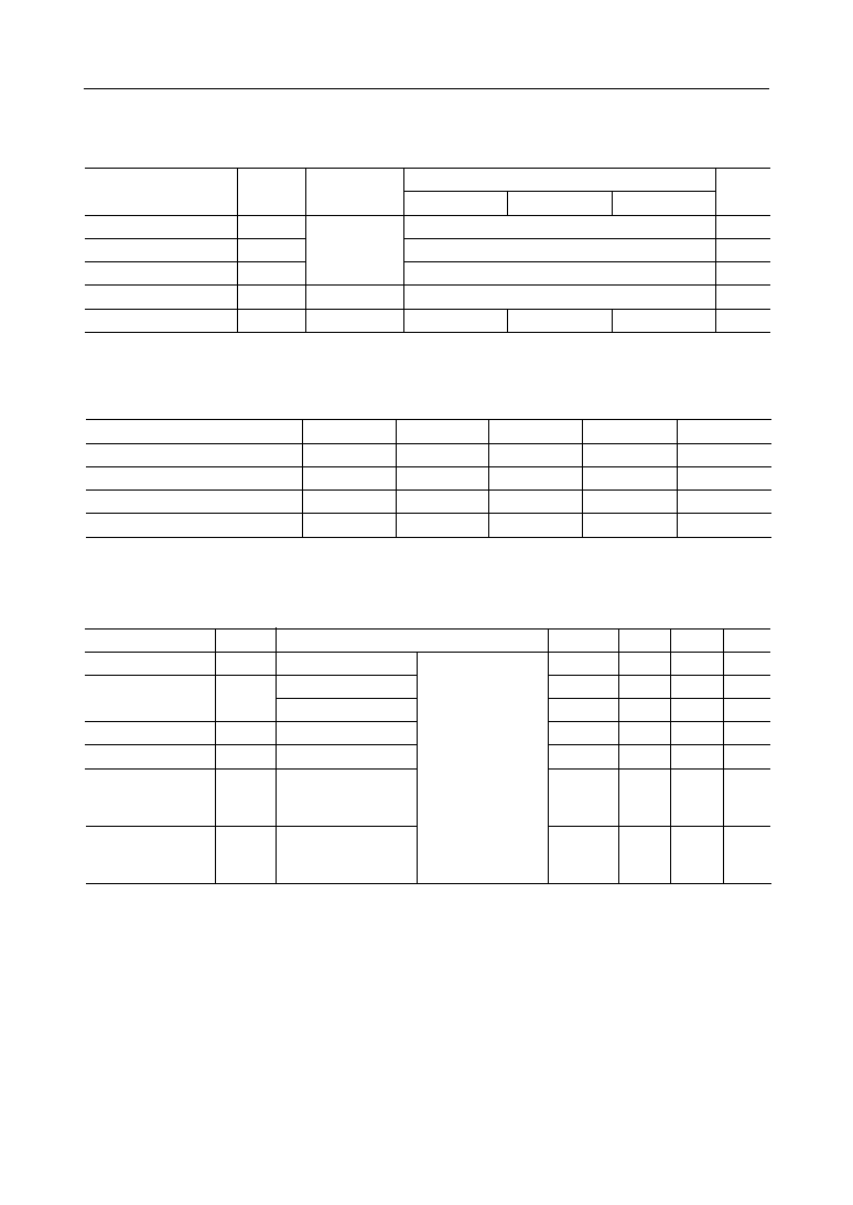
RECOMMENDED OPERATING CONDITIONS
DC CHARACTERISTICS
Typ.
Max.
"L" Output Voltage
V
OL
0.4
V
"H" Output Voltage
V
OH
--
V
--
V
Parameter
Unit
Symbol
Min.
--
3.0
V
CC
≠0.4
I
OL
= 2.5 mA
I
OH
= ≠2.5 mA
I
OH
= ≠100 mA
Conditions
V
CC
= 4.5 V to 5.5 V
Ta
= ≠40∞C to +85∞C
Input Leak Current
I
LI
10
mA
Output Leak Current
I
LO
10
mA
≠10
≠10
0 £ V
IN
£ V
CC
0 £ V
OUT
£ V
CC
cs V
CC
≠0.2 V
V
IH
V
CC
≠0.2 V
V
IH
£
0.2 V
Standby Supply
Current
I
CCS
mA
10
mA
--
--
t
CLK
=100 ns, C
L
= O pF
I
CC
Operating Supply
Curent
10
--
--
--
--
--
--
--
Typ.
Power Supply Voltage
V
CC
5
V
T
op
+25
"L" Input Voltage
V
IL
--
"H" Input Voltage
V
IH
--
Min.
4.5
≠40
≠0.5
2.2
Max.
5.5
+85
+0.8
V
CC
+ 0.5
Parameter
Unit
Symbol
∞C
V
V
Operating Temperature
5/23
° Semiconductor
MSM82C54-2RS/GS/JS
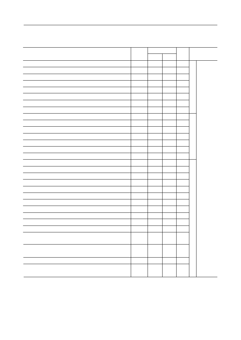
AC CHARACTERISTICS
Min.
Max.
Address Set-up Times to Falling Edge of RD
t
AR
30
--
ns
Chip Select Input Set-up Time to Falling Edge of RD
t
SR
0
--
ns
Parameter
Unit
Symbol
Conditions
Address Hold Time from Rising Edge of RD
t
RA
0
--
ns
RD Pulse Width
t
RR
95
--
ns
Data Access Time after Address Determination
t
AD
--
184
ns
Delay Time from Rising Edge of RD to Data Floting State
t
DF
5
65
ns
RD Recovery Time
t
RV
165
--
ns
Address Set-up Time to Falling Edge of WR
t
AW
0
--
ns
Chip Select Input Set-up Time to Falling Edge of WR
t
SW
0
--
ns
Address Hold Time from Rising Edge of WR
t
WA
0
--
ns
WR Pulse Width
t
WW
95
--
ns
Data Determination Set-up Time to Rising Edge of WR
t
DW
85
--
ns
Data Hold Time after Rising Edge of WR
t
WD
0
--
ns
WR Recovery Time
t
RV
165
--
ns
CLK Cycle Time
t
CLK
100
D.C.
ns
CLK "H" Level Width
t
PWH
30
--
ns
CLK "L" Level Width
t
PWL
50
--
ns
CLK Rise Time
t
r
--
25
ns
CLK Fall Time
t
f
--
25
ns
GATE "H" Level Width
t
GW
50
--
ns
GATE "L" Level Width
t
GL
50
--
ns
GATE Input Set-up Time before Rising Edge of CLK
t
GS
40
--
ns
GATE Input Hold Time before Rising Edge of CLK
t
GH
50
--
ns
Output Delay Time after Falling Edge of CLK
t
OD
--
100
ns
Output Delay Time after Falling Edge of GATE
t
ODG
--
100
ns
CLK Rise Delay Time after Rising Edge of WR for Count Value
Loading
t
WC
0
55
ns
t
WG
≠5
40
ns
GATE sampling delay time after rising edge of WR for count
loading
t
WO
--
240
ns
Output Delay Time after Falling Edge of WR for Mode Set
t
CL
≠40
40
ns
CLK Fall Set-up Time to Falling Edge of WR for Counter Latch
Command
C
L
= 150 pF
(V
CC
= 4.5 V to 5.5 V, Ta = ≠40∞C to +85∞C)
82C54-2
Data Access Time from Falling Edge of RD
t
RD
--
94
Read Timing
Write Timing
Clock Gate Timing
ns
Note:
Timing measured at V
L
= 0.8 V and V
H
= 2.2 V for both inputs and outputs.
6/23
° Semiconductor
MSM82C54-2RS/GS/JS
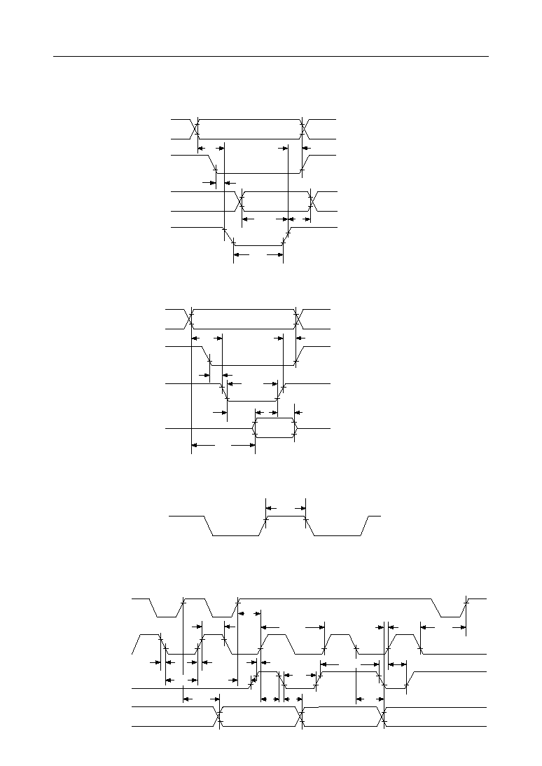
TIMING CHART
WriteTiming
Recovery Timing
Clock & Gate Timing
t
RV
RD, WR
A
0 - 1
D
0 - 7
t
AW
CS
WR
t
WA
t
SW
t
DW
t
WD
t
WW
Read Timing
A
0 - 1
RD
t
AR
CS
D
0 - 7
t
RA
t
SR
t
RR
t
RD
t
DF
t
AD
Valid
t
CL
t
GS
t
CLK
t
WC
t
PWH
t
f
t
r
t
WG
t
WO
t
GH
t
ODG
t
GL
t
OD
t
GW
t
GS
Mode
Count
Counter
Latch
WR
CLK
GATE
OUT
t
PWL
t
GH
7/23
° Semiconductor
MSM82C54-2RS/GS/JS
DESCRIPTION OF PIN FUNCTIONS
16 bits
Adress Bus
Control Bus
D
7
-
0
A
1
A
0
A
1
A
0
CS
8 bits
RD
WR
8 bits
Data Bus
MSM82C54-2
OUT GATE CLK
Counter #0
OUT GATE CLK
Counter #1
OUT GATE CLK
Counter #2
SYSTEM INTERFACING
D
7
- D
0
Name
Bidirectional
Data Bus
Input/Output
Pin Symbol
Input/Output
Function
RD
Read Input
Input
WR
Write Input
Input
A
0
, A
1
Address Input
Input
CLK
0
-
2
Clock Input
Input
GATE
0
-
2
Gate Input
Input
Three-state 8-bit bidirectional data bus used when writing control
words and count value, and reading count values upon reception of
WR and RD signals from CPU.
CS
Chip Select
Input
Input
Data transfer with the CPU is enabled when this pin is at low level.
When at high level, the data bus (D
0
thru D
7
) is switched to high
impedance state where neither writing nor reading can be executed.
Internal registers, however, remain unchanged.
Data can be transferred from MSM82C54-2 to CPU when this pin is
at low level.
Data can be transferred from CPU to MSM82C54-2 when this pin is
at low level.
One of the three internal counters or the control word register is
selected by A
0
/A
1
combination. These two pins are normally
connected to the two lower order bits of the address bus.
Supply of three clock signals to the three counters incorporated in
MSM82C54-2.
Control of starting, interruption, and restarting of counting in the
three respective counters in accordance with the set control word
contents.
OUT
0
-
2
Counter Output
Output
Output of counter output wave form in accordance with the set
mode and count value.
8/23
° Semiconductor
MSM82C54-2RS/GS/JS
DESCRIPTION OF BASIC OPERATIONS
Data transfers between the internal registers and external data bus is outlined in the following
table.
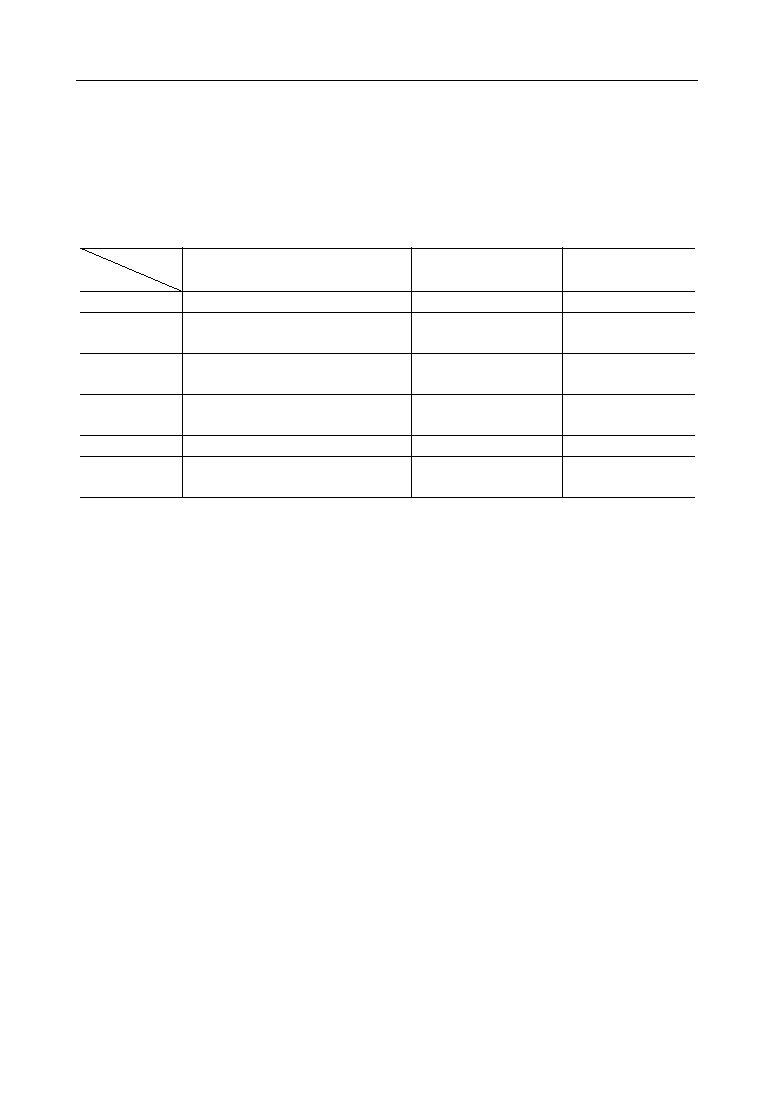
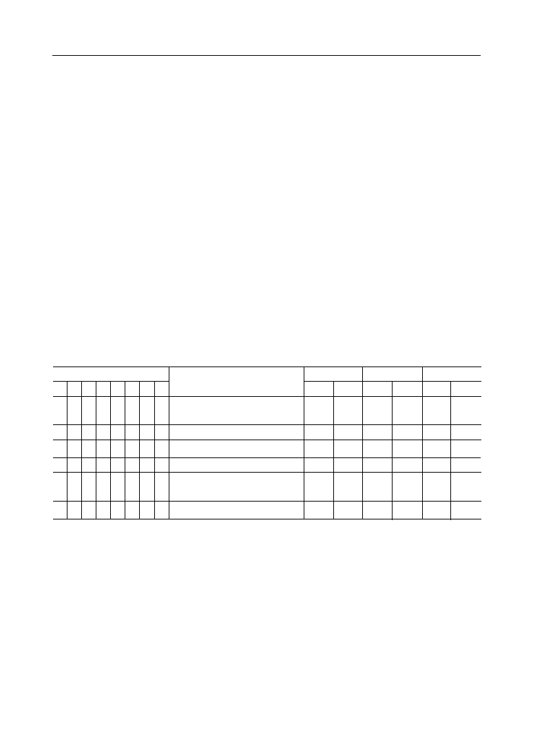
DESCRIPTION OF OPERATION
MSM82C54-2 functions are selected by control words from the CPU. In the required program
sequence, the control word setting is followed by the count value setting and execution of the
desired timer operation.
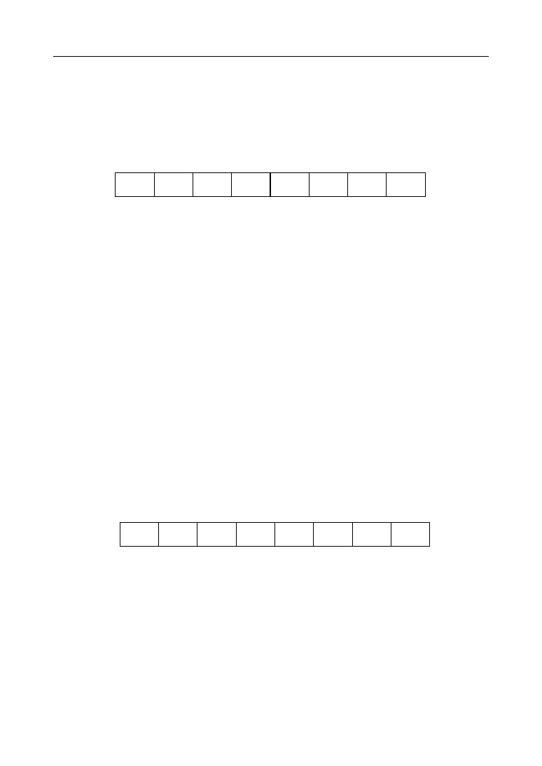
Control Word and Count Value Program
Each counter operating mode is set by control word programming. The control word format
is outlined below.
SC1
D
7
SC0
D
6
RL1
D
5
RL0
D
4
M2
D
3
M1
D
2
M0
D
1
BCD
D
0
Select Counter
Read/Load
Mode
BCD
(CS=0, A
0
, A
1
=1, 1, RD=1, WR=0)
0
0
0
0
0
CS
Function
0
0
0
1
0
1
1
1
0
1
RD
0
0
0
•
1
0
0
0
1
0
WR
1
1
1
•
1
0
1
1
0
0
A
1
0
1
1
•
•
1
0
1
0
0
A
0
1
0
1
•
•
Data Bus to Counter #0 Writing
Data Bus to Counter #1 Writing
Data Bus to Counter #2 Writing
Data Bus to Control Word Register Writing
Data Bus from Counter #0 Writing
Data Bus from Counter #1 Writing
Data Bus from Counter #2 Writing
Data Bus in High Impedance Status
•: denotes "not specified"
9/23
° Semiconductor
MSM82C54-2RS/GS/JS
∑ Select Counter (SC0, SC1):
Selection of set counter
0
1
1
0
SC1
Set Contents
1
0
1
0
SC0
Counter #0 selection
Counter #1 selection
Counter #2 selection
Read Back Command
∑ Read/Load (RL1, RL0):
Count value Reading/Loading format setting
0
1
1
0
RL1
Set Contents
1
0
1
0
RL0
Counter Latch Operation
Reading/Loading of Least Significant Byte (LSB)
Reading/Loading of Most Significant Byte (MSB)
Reading/Loading of LSB followed by MSB
∑ Mode (M2, M1, M0):
Operation waveform mode setting
∑ BCD:
Operation count mode setting
After setting Read/Load, Mode and BCD in each counter as outlined above, next set the desired
count value. (In some Modes, the count value is set first. In next clock, loading is performed,
then counting starts.) This count value setting must conform with the Read/Load format set
in advance. Note that the internal counters are reset to 0000H during control word setting. The
counter value (0000H) can't be read.
The program sequence of the MSM82C54-2 is flexible.
Free sequence programming is possible as long as the two following rules are observed:
(i) Write the control word before writing the initial count value in each counter.
(ii) Write the initial count value according to the count value read/write format specified by the
control word.
Note: Unlike the MSM82C53-2, the MSM82C54-2 allows count value setting for another
counter between LSB and MSB settings.
0
•
•
0
M2
Set Contents
0
1
1
0
M1
1
0
1
0
M0
1
1
0
0
0
1
Mode 0 (Interruput on Terminal Count)
Mode 1 (Programmable One-Shot)
Mode 2 (Rate Generator)
Mode 3 (Square Wave Generator)
Mode 4 (Software Triggered Strobe)
Mode 5 (Hardware Triggered Strobe)
•: denotes "not specified"
1
0
BCD
Set Contents
Binary Count (16-bit Binary)
BCD Count (4-decade Binary Coded Decimal)
10/23
° Semiconductor
MSM82C54-2RS/GS/JS
∑ Example of control word and count value setting
∑ The minimum and maximum count values which can be counted in each mode are listed
below.
Counter #0: Read/Load LSB only, Mode 3, Binaty count, count value 3H
Counter #1: Read/Load MSB only, Mode 5, Binaty count, count value AA00H
Counter #2: Read/Load LSB and MSB, Mode 0, BCD count, count value 1234
MVI A, 1EH
OUT n3
Counter #0 control word setting
MVI A, 6AH
OUT n3
Counter #1 control word setting
MVI A, B1H
OUT n3
Counter #2 control word setting
MVI A, 03H
OUT n0
Counter #0 count value setting
MVI A, AAH
OUT n1
Counter #1 count value setting
MVI A, 34H
OUT n2
Counter #2 count value setting (LSB then MSB)
MVI A, 12H
OUT n2
Notes: n0: Counter #0 address
n1: Counter #1 address
n2: Counter #2 address
n3: Control word register address
1
2
3
0
Mode
Remarks
1
2
2
1
MIn.
0
0
0
0
Max.
4
5
1
1
0
0
0 executes 10000H count (ditto in other mdoes)
--
1 cannot be counted
1 cannot be counted
--
--

11/23
° Semiconductor
MSM82C54-2RS/GS/JS
Internal Block Diagram of a Counter
Internal Data Bus
Control
Word
Register
Status
Latch
Status
Register
Control
Logic
CR
M
CR
L
CE
OL
M
OL
L
GATEn
CLK
n
OUT
n
NOTE : CR
M
:
CR
L
:
CE :
OL
M
:
OL
L
:
Count Register MSB
Count Register LSB
Counter Element
Output Latch MSB
Output Latch LSB

12/23
° Semiconductor
MSM82C54-2RS/GS/JS
Mode definition
Mode 0
∑ Application: Event counter
∑ Output operation: The output is set to "L" level by the control word setting, and kept at "L"
level until the counter value becomes 0.
∑ Gate function: "H" level validates the count operation, and "L" level invalidates it. The gate
does not affect the output.
∑ Count value load timing: after the control word and initial count value are written, the count
value is loaded to the CE at the falling edge of the next clock pulse. The first clock pulse does
not cause the count value to be decremented. In other words, if the initial count value is N,
the output is not set to "H" level until the input of (N+1) the clock pulse after the initial count
value writing.
∑ Count value writing during counting:
The count value is loaded in the CE at the falling edge of the next clock, and counting with the
new count value continues. The operation for 2-byte count is as follows:
1) The counting operation is suspended when the first byte is written. The output is
immediately set to "L" level. (no clock pulse is required.)
2) After the second byte is written, the new count value is loaded to the CE at the falling edge
of the next clock.
For the output to go to "H" level again, N+1 clock pulse are necessary after new count value
N is written.
∑ Count value writing when the gate signal is "L" level:
The count value is also loaded to the CE at the falling edge of the next clock pulse in this case.
When the gate signal is set to "H" level, the output is set to "H" level after the lapse of N clock
pulses. Since the count value is already loaded in the CE, no clock pulse for loading in the CE
is necessary.
Mode 1
∑ Application: Digital one-shot
∑ Output operation: The output is set to "H" level by the control word setting. It is set to "L"
level at the falling edge of the clock succeeding the gate trigger, and kept at "L" level until the
counter value becomes 0. Once the output is set to "H" level, it is kept at "H" level until the
clock pulse succeeding the next trigger pulse.
∑ Count value load timing:
After the control word and initial count value are written, the count value is loaded to the CE
at the falling edge of the clock pulse succeeding the gate trigger and set the output to "L" level.
The one-shot pulse starts in this way. If the initial count value is N, the one-shot pulse interval
equals N clock pulses. The one-shot pulse is not repetitive.
∑ Gate function: The gate signal setting to "L" level after the gate trigger does not affect the
output. When it is set to "H" level again from "L" level, gate retriggering occurs, the CR count
value is loaded again, and counting continues.
∑ Count value writing during counting
It does not affect the one-shot pulse being counted until retriggering occurs.

13/23
° Semiconductor
MSM82C54-2RS/GS/JS
Mode 2
∑ Application: Rate generator, real-time interrupt clock.
∑ Output operation: The output is set to "H" level by control word setting. When the initial
count value is decremented to 1, the output is set to "L" level during one clock pulse, and is
then set to "H" level again. The initial count value is reloaded, and the above sequence
repeats. In mode 2, the same sequence is repeated at intervals of N clock pulses if the initial
count value is N for example.
∑ Gate function: "H" level validates counting, and "L" level invalidates it. If the gate signal is
set to "L" level when the output pulse is "L" level, the output is immediately set to "H" level.
At the falling edge of the clock pulse succeeding the trigger, the count value is reloaded and
counting starts. The gate input can be used for counter synchronization in this way.
∑ Count value load timing:
After the control word and initial count value is written, the count value is loaded to the CE
at the falling edge of the next clock pulse. The output is set to "L" level upon lapse of N clock
pulses after writing the initial count value N. Counter synchronization By software is possible
in this way.
∑ Count value writing during counting:
Count value writing does not affect the current counting operation sequence. If new count
value writing completes and the gate trigger arrives before the end of current counting
operation, the count value is loaded to the CE at the falling edge of next clock pulse and
counting continues from the new count value. If no gate trigger arrives, the new count value
is loaded to the CE at the end of the current counting operation cycle. In mode 2, count value
of 1 is prohibited.
Mode 3
∑ Application: Baud rate generator, square wave generator
∑ Output operation: Same as mode 2 except that the output duty is different.
The output is set to "H" level by control word setting. When the count becomes half the initial
count value, the output is set to "L" level and kept at "L" level during the remainder of the
count. Mode 3 repeats the above sequence periodically. If the initial count value is N, the
output becomes a square wave with a period of N.
∑ Gate operation: "H" level validates counting, and "L" level invalidates it. If the gate signal
is set to "L" level when the output is "L" level, the output is immediately set to "H" level. The
initial count value is reloaded at the falling edge of the clock pulse succeeding the next gate
trigger. The gate can be used for counter synchronization in this way.
∑ Count value load timing:
After the control word and initial count value are written, the count value is loaded to the CE
at the falling edge of the next clock pulse, Counter synchronization by software is possible
in this way.
∑ Count value writing during counting:
The count value writing does not affect the current counting operation. When the gate trigger
input arrives before the end of a half cycle of the square wave after writing the new count
value, the new count value is loaded in the CE at the falling edge of the next clock pulse, and
counting continues using the new count value. If there is no gate trigger, the new count value
is loaded at the end of the half cycle and counting continues.
∑ Even number counting operation:
The output is initially set to "H" level. The initial count value is loaded to the CE at the falling
edge of the next clock pulse, and is decremented by 2 by consecutive clock pulses. When the
counter value becomes 2, the output is set to "L" level, the initial value is reloaded and then
the above operation is repeated.

14/23
° Semiconductor
MSM82C54-2RS/GS/JS
∑ Odd number counting operation:
The output is initially set to "H" level. At the falling edge of the next clock pulse, the initial
count value minus one is loaded in the CE, and then the value is decremented by 2 by
consecutive clock pulses. When the counter value becomes 0, the output is set to "L" level,
and then the initial count value minus 1 is reloaded to the CE. The value is then decremented
by 2 by consecutive clock pulses. When the counter value becomes 2, the output is again set
to "H" level and the initial count value minus 1 is again reloaded. The above operations are
repeated. In other words, the output is set to "H" level during (N+1)/2 counting and to "L"
level during (N-1)/2 counting in the case of odd number counting.
Mode 4
∑ Application: Software trigger strobe
∑ Output operation: The output is initially set to "H" level. When the counter value becomes
0, the output goes to "L" level during one clock pulse, and then restores "H" level again.
The count sequence starts when the initial count value is written.
∑ Gate function: "H" level validates counting, and "L" level invalidates counting. The gate
signal does not affect the output.
∑ Count value load timing:
After the control word and initial count value are written, the count value is loaded to the CE
at the falling edge of the next clock pulse. The clock pulse does not decrement the initial count
value. If the initial count value is N, the strobe is not output unless N+1 clock pulses are input
after the initial count value is written,
∑ Count value writing during counting:
The new count value is written to the CE at the falling edge of the next clock pulse, and
counting continues using the new count value. The operation for 2-byte count is as follows:
1) First byte writing does not affect the counting operation.
2) After the second byte is written, the new count value is loaded to the CE at the falling edge
of the next clock pulse.
This means that the counting operation is retriggered by software. The output strobe is set to
"L" level upon input of N+1 clock pulses after the new count value N is written.
Mode 5
∑ Application: Hardware trigger strobe
∑ Output operation:
The output is initially set to "H" level. When the counter value becomes 0 after triggering by
the rising edge of the gate pulse, the output goes to "L" level during one clock pulse, and then
restores "H" level.
∑ Count value load timing:
Even after the control word and initial count value are written, loading to the CE does not
occur until the input of the clock pulse succeeding the trigger. For the clock pulse for CE
loading, the count value is not decremented. If the initial count value is N, therefore, the
output is not set to "L" level until N+1 clock pulses are input after triggering.
∑ Gate function:
The initial count value is loaded to the CE at the falling edge of the clock pulse succeeding gate
triggering. The count sequence can be retriggered.
The gate pulse does not affect the output.
15/23
° Semiconductor
MSM82C54-2RS/GS/JS
∑ Count value writing during counting:
The count value writing does not affect the current counting sequence. If the gate trigger is
generated after the new count value is written and before the current counting ends, the new
count value is loaded to the CE at the falling edge of the next clock pulse, and counting
continues using the new count value. The various roles of the gate input signals in the above
modes are summarized in the following table.
0
1
"H" Level
"L" Level Falling Edge
Rising Edge
Mode
Gate
Counting not possible
Counting possible
(1)
(2)
Start of counting
Retriggering
2
(1)
(2)
Counting not possible
Counter output forced to "H" level
Start of counting
Counting possible
3
(1)
(2)
Counting not possible
Counter output forced to "H" level
Start of counting
Counting possible
4
Counting not possible
Counting possible
5
(1)
(2)
Start of counting
Retriggering
16/23
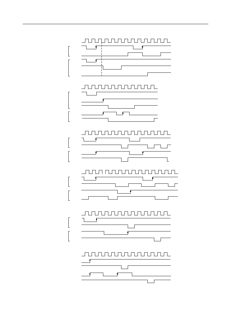
° Semiconductor
MSM82C54-2RS/GS/JS
4
3
2
1
0
2
1
0
(n=2)
(n=4)
(GATE = "H")
4
3
2
1
0
CLK
WR
OUT
WR
GATE
OUT
(n=4)
Mode 0
Mode 1
4
3
2
1
0
(n=4)
CLK
WR
GATE
OUT
GATE
OUT
4
3
2
4
3
2
1
0
(n=4)
4
3
2
1
4
1
2
1
(n=2)
(n=4)
(GATE = "H")
CLK
WR
OUT
GATE
OUT
4
3
2
1
4
3
2
2
4
3
2
1
Mode 2
4
2
4
2
4
(n=4)
CLK
WR
OUT
GATE
OUT (n=5)
Mode 3
(n=3)
2
4
2
3
2
3
3
4
2
0
4
2
4
2
0
4
2
4
2
(GATE = "H")
4
3
2
1
0
CLK
WR
OUT
GATE
OUT
3
2
1
0
Mode 4
(GATE = "H")
4
4
3
2
1
0
(n=4)
CLK
GATE
OUT
GATE
OUT
2
1
0
Mode 5
4
3
2
1
4
3
(n=4)
Note : "n" is the value set in the counter.
Figures in these diagrams refer to counter values.
(n=4)
17/23
° Semiconductor
MSM82C54-2RS/GS/JS
Reading Counter Values
All MSM82C54-2 counting is down-counting, the counting being in steps of 2 in mode 3.
Counter values can be read during counting by. (1) direct reading, (2) counter latching ("read
on the fly"), and (3) read back command.
(1) Direct reading
Counter values can be read by direct reading operations.
Since the counter value read according to the timing of the RD and CLK signals is not
guaranteed, it is necessary to stop the counting by a gate input signal, or to interrupt the
clock input temporarily by an external circuit to ensure that the counter value is correctly
read.
(2) Counter latching
In this method, the counter value is latched by writing counter latch command, thereby
enabling a stable value to be read without effecting the counting in any way at all. The
output latch (OL) of the selected counter latches the count value when a counter latch
command is written. The count value is held until it is read by the CPU or the control word
is set again.
If a counter latch command is written again before reading while a certain counter is latched,
the second counter latch command is ignored and the value latched by the first counter latch
command is maintained.
The MSM82C54-2 features independent reading and writing from and to the same counter.
When a counter is programmed for the 2-byte counter value, the following sequence is
possible:
1. Count value (LSB) reading
2. New count value (LSB) writing
3. Count value (MSB) reading
4. New count value (MSB) writing
An example of a counter latching program is given below.
Counter latching executed for counter #1 (Read/Load 2-byte setting)
0 1 0 0 • • • •
MVI A
Denotes counter latching
OUT n3
Write in control word address (n3)
IN n1
Reading of the LSB of the counter value
latched from counter #1.
n1: Conter #1 address
MOV B, A
IN n1
MOV C, A
Reading of MSB from counter #1
The counter value at this point is latching
18/23
° Semiconductor
MSM82C54-2RS/GS/JS
(3) Read Back Command Operation
Use of the read back command enables the user to check the count value, program mode,
output pin state and null count flag of the selected counter.
The command is written in the control word register, and the format is as shown below. For
this command, the counter selection occurs according to bits D
3
, D
2
and D
1
.
It is possible to latch multiple counters by using the read back command. Latching of a read
counter is automatically canceled but other counters are kept latched. If multiple read back
commands are written for the same counter, commands other than the first one are ignored.
It is also possible to latch the status information of each counter by using the read back
command. The status of a certain counter is read when the counter is read. The counter
status format is as follows:
Bits D
5
to D
0
indicate the mode programmed by the most recently written control word.
Bit D
7
indicates the status of the output pin.
Use of this bit makes it possible to monitor the counter output, so the corresponding
hardware may be omitted.
OUTPUT
D
7
NULL
COUNT
D
6
RL1
D
5
RL0
D
4
M2
D
3
M1
D
2
M0
D
1
BCD
D
0
D
7
: 1 = Output pin status is 1.
0 = Output pin status is 0.
D
6
: 1 = Null count
0 = Count value reading is effective
D
5
- D
0
: Programmed mode of counter
(See the control word format.)
1
D
7
1
D
6
COUNT
D
5
STATUS
D
4
CNT2
D
3
CNT1
D
2
CNT0
D
1
0
D
0
(CS=0, A
0
, A
1
=1, RD=1, WR=0)
D
5
: 0 = Selected counter latch operation
D
4
: 0 = Selected counter status latch operation
D
3
: 1 = Counter #2 selection
D
2
: 1 = Counter #1 selection
D
1
: 1 = Counter #0 selection
D
0
: 0
=
Fixed
19/23
° Semiconductor
MSM82C54-2RS/GS/JS
Null count indicates the count value finally written in the counter register (CR) has been
loaded in the counter element (CE). The time when the count value was loaded in the CE
depends on the mode of each counter, and it cannot be known by reading the counter value
because the count value does not tell the new count value if the counter is latched. The null
count operation is shown below.
Operation
Result
A. Control word register writing
Null count = 1
B. Count register (CR) writing
Null count = 1
C. New count loading to CE (CR∆CE)
Null count = 0
Note: The null count operation for each counter is independent. When the 2-byte count
is programmed, the null count is set to 1 when the count value of the second byte
is written.
If status latching is carried out multiple times before status reading, other than the first
status latch is ignored.
Simultaneous latching of the count and status of the selected counter is also possible. For
this purpose, set bits D
4
and D
3
, COUNT and STATUS bits, to 00. This is functionally the
same as writing two separate read back commands at the same time. If counter/status
latching is carried out multiple times before each reading, other than the first one is ignored
here again. The example is shown below.
Note:
The latch command at this time point is ignored, and the first latch command is valid.
If both the count and status are latched, the status latched in the first counter read operation
is read. The order of count latching and status latching is irrelevant.
The count(s) of the next one or two reading operations is or are read.
Note:
There is the possibility of glitch noise in the output low level when reading out the data.
Peak voltage in typical condition (5 V, 25
∞
C) is approximately 1V and in the worst
condition (5.5 V, ≠40
∞
C) is approximately 1.4V.
Counter 0
Counter 1
Command
Counter 2
Contents
D
7
D
6
D
5
D
4
D
3
D
2
D
1
D
0
1
0
0
0
0
1
0
1
1
0
0
1
0
0
1
1
0
1
1
0
0
1
0
1
1
0
0
0
1
0
0
0
1
0
0
1
1
0
0
0
1
0
Count Status Count Status Count Status
Read back status and count
(counter 0)
Read back status (counter 1)
Read back status (counter 1 and 2)
Read back status (counter 2)
Read back status and count
(counter 1)
Read back status (counter 0)
L
(NOTE)
(NOTE)
(NOTE)
L
--
--
--
--
L
L
--
L
--
--
L
L
--
L
--
L
L
L
--
L
L
L
L
L
L
L
L
L
L
L
L
L
L
L
1
1
1
1
1
1
20/23
° Semiconductor
MSM82C54-2RS/GS/JS
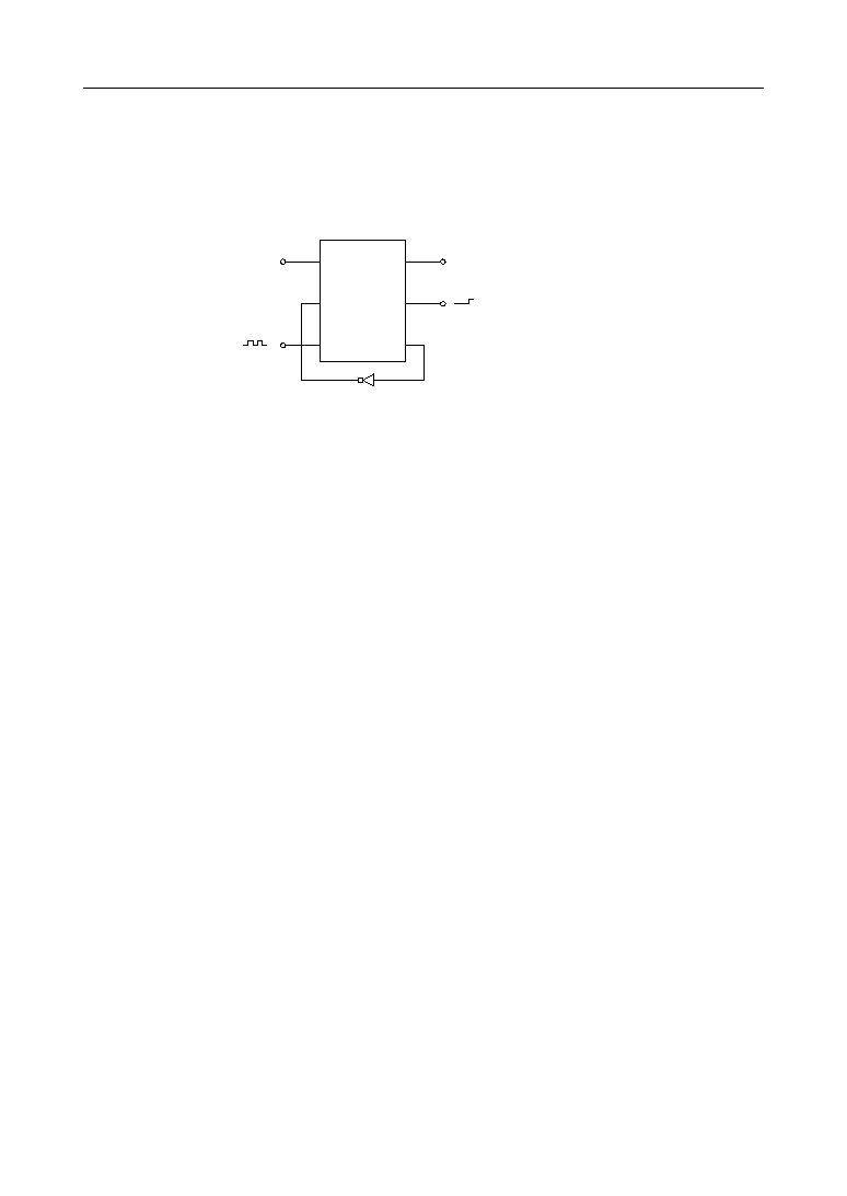
Example of Practical Application
∑ MSM82C54-2 used as a 32-bit counter.
MSM82C54 -2
CLK
0
OUT
0
CLK
1
OUT
1
CLK
2
OUT
2
Use counter #1 and counter #2
Counter #1: mode 0, upper order 16-bit counter value
Counter #2: mode 2, lower order 16-bit counter value
This setting enables counting up to a maximum of 2
32
.
21/23
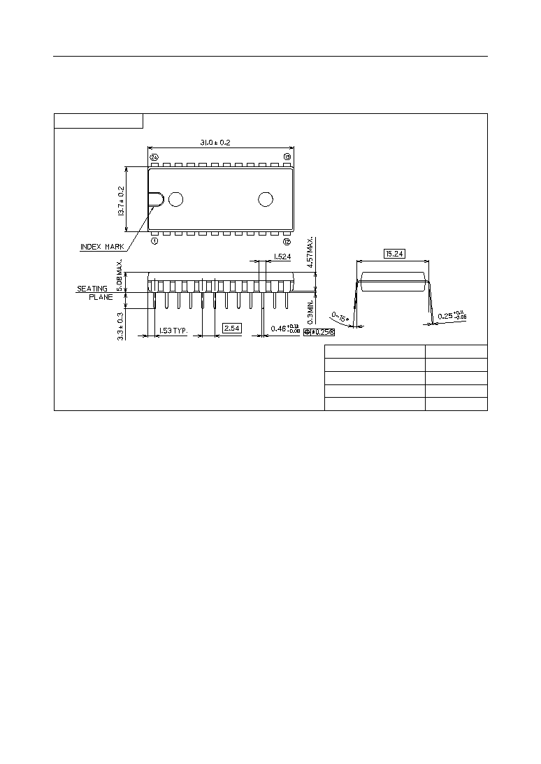
° Semiconductor
MSM82C54-2RS/GS/JS
(Unit : mm)
PACKAGE DIMENSIONS
Notes for Mounting the Surface Mount Type Package
The SOP, QFP, TSOP, SOJ, QFJ (PLCC), SHP and BGA are surface mount type packages, which
are very susceptible to heat in reflow mounting and humidity absorbed in storage.
Therefore, before you perform reflow mounting, contact Oki's responsible sales person for the
product name, package name, pin number, package code and desired mounting conditions
(reflow method, temperature and times).
DIP24-P-600-2.54
Package material
Lead frame material
Pin treatment
Solder plate thickness
Package weight (g)
Epoxy resin
42 alloy
Solder plating
5 mm or more
3.55 TYP.
22/23
° Semiconductor
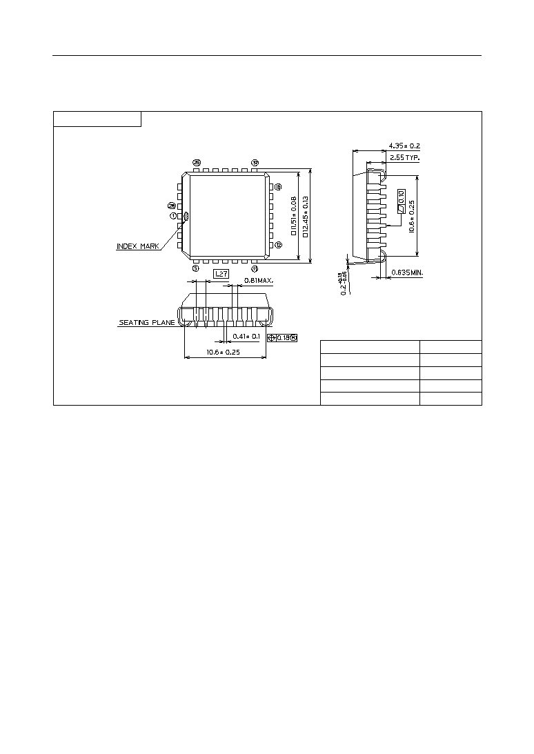
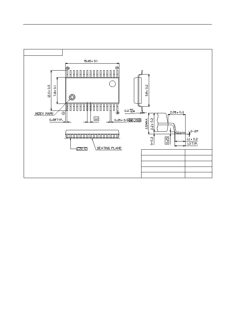
MSM82C54-2RS/GS/JS
(Unit : mm)
Notes for Mounting the Surface Mount Type Package
The SOP, QFP, TSOP, SOJ, QFJ (PLCC), SHP and BGA are surface mount type packages, which
are very susceptible to heat in reflow mounting and humidity absorbed in storage.
Therefore, before you perform reflow mounting, contact Oki's responsible sales person for the
product name, package name, pin number, package code and desired mounting conditions
(reflow method, temperature and times).
QFJ28-P-S450-1.27
Package material
Lead frame material
Pin treatment
Solder plate thickness
Package weight (g)
Epoxy resin
Cu alloy
Solder plating
5 mm or more
1.00 TYP.
Spherical surface
23/23
° Semiconductor
MSM82C54-2RS/GS/JS
(Unit : mm)
Notes for Mounting the Surface Mount Type Package
The SOP, QFP, TSOP, SOJ, QFJ (PLCC), SHP and BGA are surface mount type packages, which
are very susceptible to heat in reflow mounting and humidity absorbed in storage.
Therefore, before you perform reflow mounting, contact Oki's responsible sales person for the
product name, package name, pin number, package code and desired mounting conditions
(reflow method, temperature and times).
SSOP32-P-430-1.00-K
Package material
Lead frame material
Pin treatment
Solder plate thickness
Package weight (g)
Epoxy resin
42 alloy
Solder plating
5 mm or more
0.60 TYP.
Mirror finish