 | –≠–ª–µ–∫—Ç—Ä–æ–Ω–Ω—ã–π –∫–æ–º–ø–æ–Ω–µ–Ω—Ç: MSM82C84A | –°–∫–∞—á–∞—Ç—å:  PDF PDF  ZIP ZIP |
1/18
° Semiconductor
MSM82C84A-2RS/GS/JS
GENERAL DESCRIPTION
The MSM82C84A-2RS/GS is a clock generator designed to generate MSM80C86A-10 and
MSM80C88A-10 system clocks of 8MHz.
Due to the use of silicon gate CMOS technology, standby current is only 40 mA (MAX.), and the
power consumption is very low with 16 mA (MAX.) when a 8 MHz clock is generated.
FEATURES
∑ Operating frequency of 6 to 24 MHz (CLK output 2 to 8 MHz)
∑ 3 m silicon gate CMOS technology for low power consumption
∑ Built-in crystal oscillator circuit
∑ 3 V to 6 V single power supply
∑ Built-in synchronized circuit for MSM80C86A-10 and MSM80C88A-10 READY and RESET
∑ TTL compatible
∑ Built-in Schmitt trigger circuit (RES input)
∑ 18-pin Plastic DIP (DIP18-P-300-2.54): (Product name: MSM82C84A-2RS)
∑ 20-pin Plastic QFJ (QFJ20-P-S350-1.27): (Product name: MSM82C84A-2JS)
∑ 24-pin Plastic SOP (SOP24-P-430-1.27-K): (Product name: MSM82C84A-2GS-K)
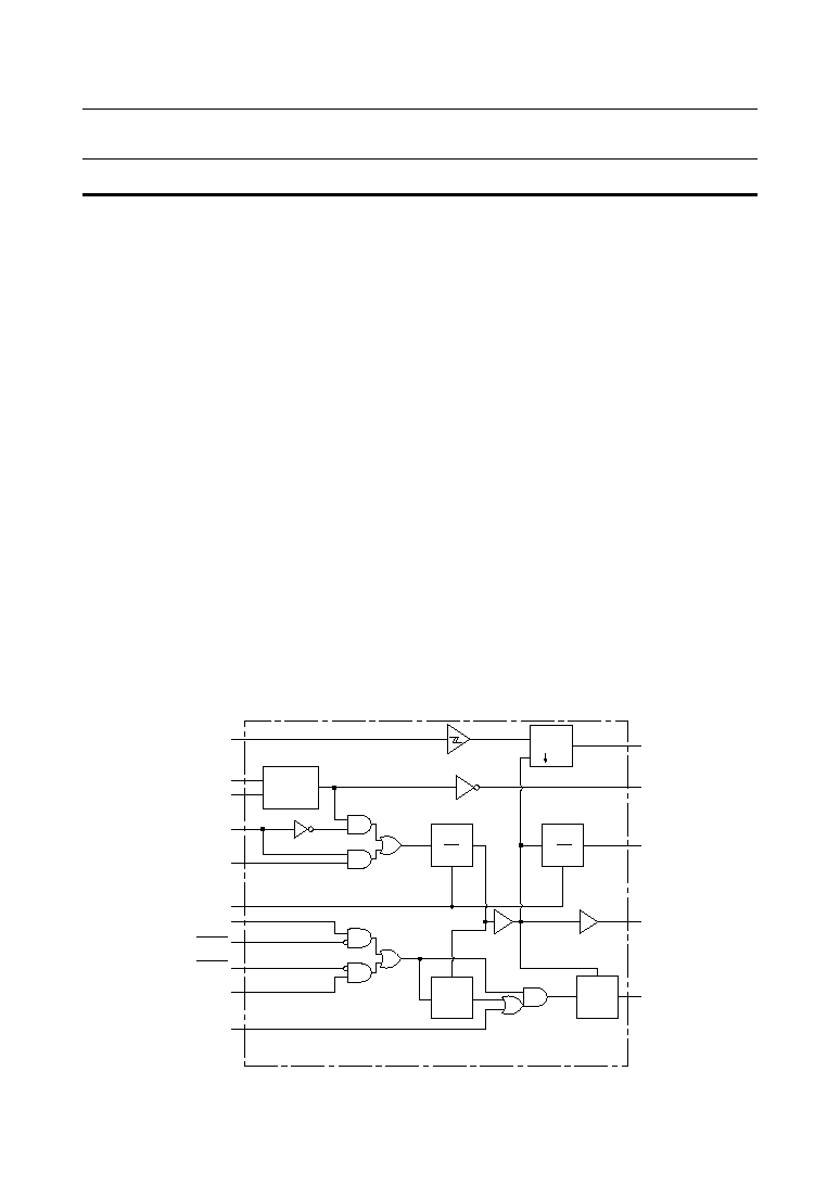
FUNCTIONAL BLOCK DIAGRAM
° Semiconductor
MSM82C84A-2RS/GS/JS
CLOCK GENERATOR AND DRIVER
RESET
OSC
PCLK
CLK
READY
D
C
Q
1
2
1
3
S
Y
N
C
S
Y
N
C
D
C
ÿ
Q
(F2)
D
C
Q
(F1)
RES
x
1
x
2
F/C
EFI
CSYNC
RDY
1
AEN
1
AEN
2
ASYNC
RDY
2
Crystal
Oscillator
E2O0012-27-X2
This version: Jan. 1998
Previous version: Aug. 1996
2/18
° Semiconductor
MSM82C84A-2RS/GS/JS
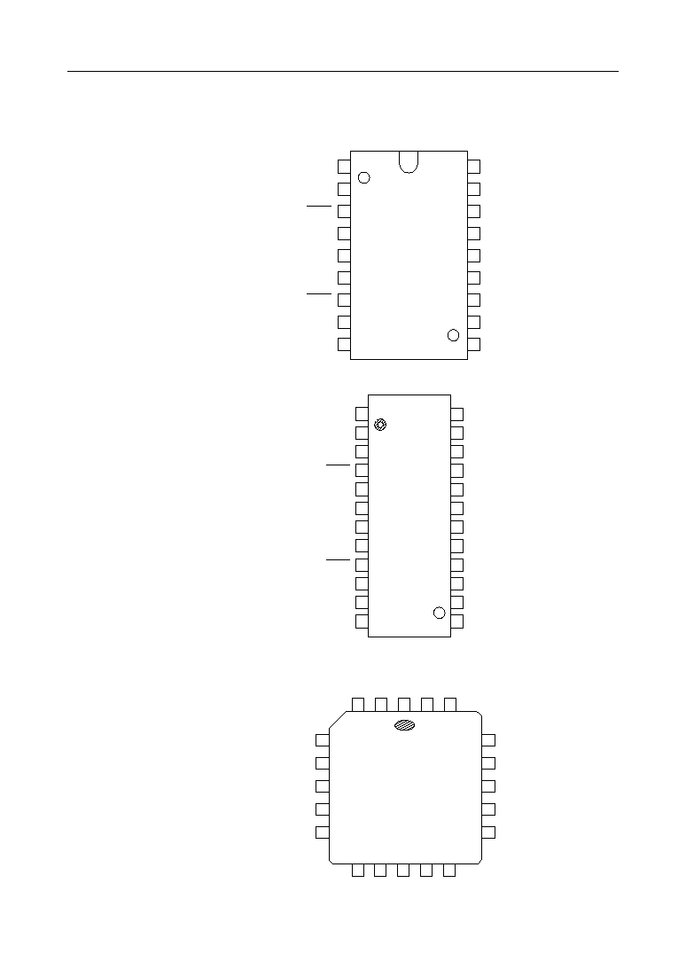
PIN CONFIGURATION (TOP VIEW)
18 pin Plastic DIP
24 pin Plastic SOP
20 pin Plastic QFJ
18
17
16
15
14
RDY
2
AEN
2
RDY
1
READY
NC
9
10
11
12
13
CLK
GND
RESET
RES
OSC
3
2
1
20
19
AEN
1
PCLK
CSYNC
X
1
4
5
6
7
8
V
CC
ASYNC
EFI
F/C
NC
X
2
X
2
NC
ASYNC
EFI
NC
F/C
OSC
NC
X
1
RES
RESET
NC
AEN
1
RDY
1
READY
NC
RDY2
AEN
2
NC
CSYNC
PCLK
CLK
GND
1
2
3
4
5
6
7
8
9
10
11
12
24
23
22
21
20
19
18
17
16
15
14
13
Vcc
1
2
3
4
5
6
7
8
9
18
17
16
15
14
13
12
11
10
ASYNC
EFI
F/C
OSC
X
2
X
1
RES
RESET
AEN
1
RDY
1
READY
RDY
2
AEN
2
CSYNC
PCLK
CLK
GND
V
CC
(NC not connected)
3/18
° Semiconductor
MSM82C84A-2RS/GS/JS
ABSOLUTE MAXIMUM RATINGS
≠55 to +150
MSM82C84A-2RS/JS
Supply Voltage
V
CC
≠0.5 to +7
V
Input Voltage
V
IN
≠0.5 to V
CC
+0.5
V
Output Voltage
V
OUT
≠0.5 to V
CC
+0.5
V
Storage Temperature
T
STG
∞C
Power Dissipation
P
D
W
Parameter
Unit
Symbol
Respect
to GND
--
Ta = 25∞C
Condition
Rating
MSM82C84A-2GS
0.7
0.8
OPERATING RANGES
Range
Supply Voltage
V
CC
3 to 6
V
Operating Temperature
T
op
≠40 to +85
∞C
Parameter
Unit
Symbol
RECOMMENDED OPERATING CONDITIONS
DC CHARACTERISTICS
Max.
"L" Level Output Voltage (CLK)
V
OL
0.4
V
"H" Output Voltage (CLK)
V
OL
0.4
V
Parameter
Unit
Symbol
Min.
--
--
V
CC
≠0.4
I
OL
= 4 mA
I
OL
= 2.5 mA
I
OH
= ≠4 mA
Condition
"H" Output Voltage (Others)
V
OH
--
V
V
CC
≠0.4
I
OH
= ≠1 mA
RES Input Hysteresis
V
IHR
-V
ILR
--
V
0.2*V
CC
Input Leak Current
(Except ASYNC)
I
LI
+1
mA
≠1
0 £ V
IN
£ V
CC
Input Current (ASYNC)
I
LIA
+10
mA
≠100
0 £ V
IN
£ V
CC
Standby Supply Current
I
CCS
40
mA
--
Note 1
Input Capacitance
C
IN
7
pF
f =1 MHz
--
"L" Level Output Voltage (Others)
Operating Supply Current
--
V
OH
--
V
I
CC
16
mA
f = 24 MHz, C
L
= O
P
F
(V
CC
= 5 V ± 10%, Ta = ≠40 to 85∞C)
Note:
1. X1
V
CC
≠ 0.2 V, X2 £ 0.2 V
F/C
V
CC
≠ 0.2 V, ASYNC = V
CC
or open
VIH
V
CC
≠ 0.2 V, VIL £ 0.2 V
Typ.
Supply Voltage
V
CC
5
V
T
op
+25
"L" Level Input Voltage
V
IL
V
IH
--
"H" Level Input Voltage (except RES)
--
Min.
4.5
≠40
≠0.5
2.2
Max.
5.5
+85
+0.8
V
CC
+0.5
Parameter
Unit
Symbol
∞C
V
V
0.6*V
CC
Operating Temperature
"H" Level Input Voltage (RES)

4/18
° Semiconductor
MSM82C84A-2RS/GS/JS
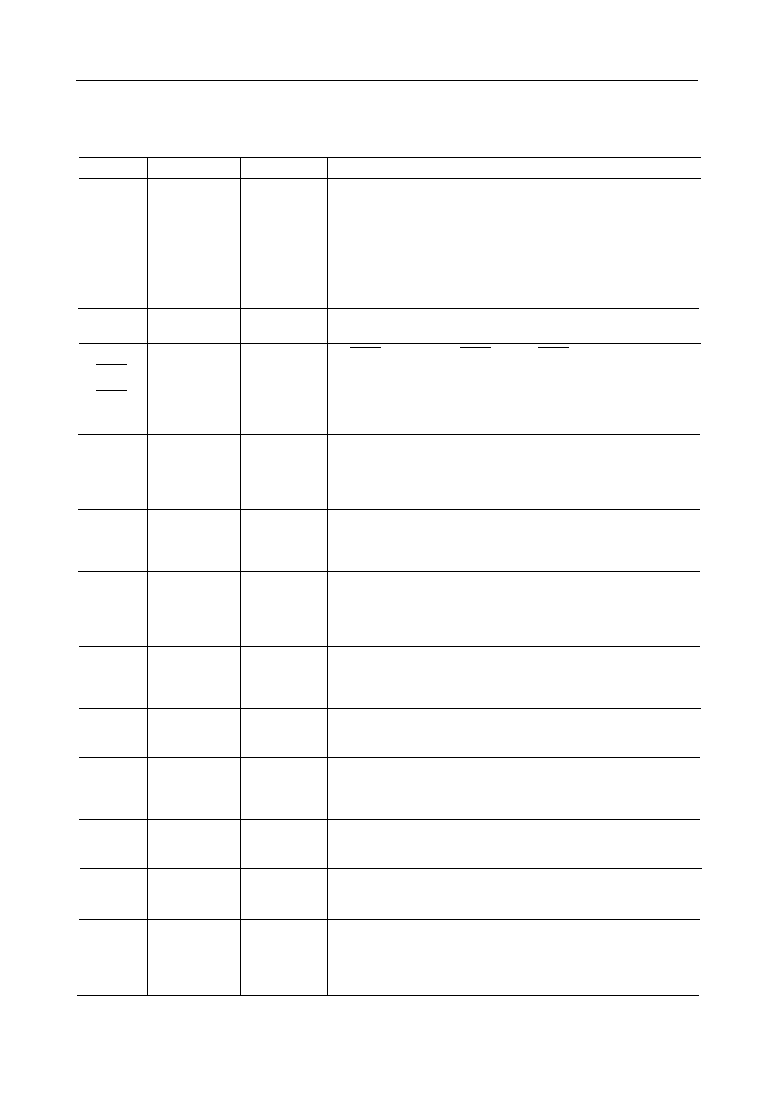
AC CHARACTERISTICS
(1)
Parameter
Symbol
Min.
Max.
Unit
EFI "H" Pulse Width
EFI "L" Pulse Width
Crystal Oscillator Frequency
Set up Time of RDY
1
or RDY
2
to
CLK Falling Edge (Active)
EFI Cycle Time
Conditions
Set up Time of RDY
1
or RDY
2
to
CLK Rising Edge (Active)
Set up Time of RDY
1
or RDY
2
to
CLK Falling Edge (Inactive)
Hold Time of RDY
1
or RDY
2
to
CLK Falling Edge
Set up Time of ASYNC to CLK
Falling Edge
Hold Time of ASYNC to
CLK Falling Edge
Set up Time of AEN
1
(AEN
2
) to
RDY
1
(RDY
2
) Rising Edge
Hold Time of AEN
1
(AEN
2
) to
CLK Falling Edge
Set up Time of CSYNC to EFI
Rising Edge
Hold Time of CSYNC to EFI
Rising Edge
CSYNC Pulse Width
Set up Time of RES to CLK Falling
Edge
Hold Time of RES to CLK Falling
Edge
Input Rising Edge Time
Input Falling Edge Time
t
EHEL
t
ELEH
t
ELEL
t
R1VCL
t
R1VCH
t
R1VCL
t
CLR1X
t
AYVCL
t
CLAYX
t
A1R1V
t
CLA1X
t
YHEH
t
YHYL
t
I1HCL
t
CLI1H
t
ILIH
t
IHIL
t
EHYL
--
13
17
36
6
35
35
35
0
50
0
15
0
20
10
2 •
t
ELEL
65
20
--
--
24
--
--
--
--
--
--
--
--
--
--
--
--
--
--
--
--
15
15
ns
ns
ns
ns
ns
ns
ns
ns
ns
ns
ns
ns
ns
MHz
ns
ns
ns
ns
ns
90% to 90%
10% to 10%
--
--
ASYNC
= High
ASYNC
= Low
--
--
--
--
--
--
--
--
--
--
--
--
--
Output Load
Capacitance
CLK output
C
L
= 100 pF
Others 30 pF
(V
CC
= 5 V ± 10%, Ta = ≠40 to 85∞C)
Note: Parameters where timing has not been indicated in the above table are measured at
V
L
= 1.5 V and V
H
= 1.5 V for both inputs and outputs.
5/18
° Semiconductor
MSM82C84A-2RS/GS/JS
AC CHARACTERISTICS
(2)
Parameter
Symbol
Min.
Max.
Unit
CLK Cycle Time
CLK "H" Pulse Width
CLK Rising and Falling Edge
Times
CLK "L" Pulse Width
Conditions
PCLK "H" Pulse Width
Time from READY Falling Edge
to CLK Falling Edge
Time from READY Rising Edge
to CLK Rising Edge
Delay from CLK Falling Edge
to RESET Falling Edge
Delay from CLK Falling Edge
to PCLK Rising Edge
Delay from CLK Falling Edge
to PCLK Falling Edge
Delay from OSC Falling Edge
to CLK Falling Edge
Output Rising Edge Time
(Except CLK)
Output Falling Edge Time
(Except CLK)
t
CLCL
t
CHCL
t
CLCH
t
CH1CH2
t
PHPL
t
RYLCL
t
RYHCH
t
CLIL
t
CLPH
t
CLPL
t
OLCL
t
OLOH
t
OHOL
125
--
T
CLCL
≠20
-8
--
--
--
2
--
--
10
--
--
--
40
22
22
35
--
--
--
15
15
ns
ns
ns
ns
ns
ns
ns
ns
ns
ns
ns
ns
ns
--
Output Load
Capacitance
CLK Output
C
L
= 100 pF
Others 30 pF
(V
CC
= 5 V ± 10%, Ta = -40 to 85∞C)
PCLK "L" Pulse Width
t
CL2CL1
t
PLPH
Delay from OSC Falling Edge
to CLK Rising Edge
t
OLCH
1
3
T
CLCL
+ 2
2
3
T
CLCL
≠15
T
CLCL
≠20
2
3
T
CLCL
≠15
≠5
--
22
ns
--
--
1.0 V to 3.5 V
--
--
--
--
--
--
--
--
--
0.8 V to 2.2 V
2.2 V to 0.8 V
Note: Parameters where timing has not been indicated in the above table are measured at
V
L
= 1.5 V and V
H
= 1.5 V for both inputs and outputs.
6/18
° Semiconductor
MSM82C84A-2RS/GS/JS
PIN DESCRIPTION
CSYNC
Name
Clock
Synchronization
Single
Input
Pin Symbol
Input/Output
Function
AEN
1
AEN
2
Address Enable
Signals
Input
RDY
1
RDY
2
Bus Ready
Signals
Input
READY
Ready Output
Output
CLK
Clock Output
Output
RES
Reset in
Input
Synchronizing signal for output of in-phase CLK signals when more
than one MSM82C84A-2 is used.
The internal counter is reset when this signal is at high level, and a
high level CLK output is generated. The internal counter is
subsequently activated and a 33% duty CLK output is generated when
this signal is switched to low level.
When this signal is used, external synchronization of EFI is necessary.
When the internal oscillator is used, it is necessary for this pin to be
kept to be low level.
PCLK
Output
This peripheral circuit clock signal is output in a 50% duty cycle at
a frequency half that of the clock signal.
The AEN
1
signal enables RDY
1
, and the AEN
2
signal RDY
2
.
The respective RDY inputs are activated when the level applied to
these pins is low.
Although two separate inputs are used in multi-master systems, only
the AEN which enables the RDY input to be used is to be switched to
low level in the case of not using multi-master systems.
Completion of data bus reading and writing by the device connected
to the system data bus is indicated when one of these signals is
switched to high level.
The relevant RDY input is enables only when the corresponding AEN
is at low level.
This signal is obtained by synchronizing the bus ready signal with
CLK.
This signal is output after guaranteeing the hold time for the
CPU in phase with the RDY input.
This signal is the clock used by the CPU and peripheral devices
connected to the CPU system data bus. The output waveform is
generated in a 33% duty cycle at a frequency 1/3 the oscillating
frequency of the crystal oscillator connected to the X
1
and X
2
pins,
or at a frequency 1/3 the EFI input frequency.
This low-level active input is used to generate a CPU reset signal.
Since a Schmitt trigger is included in the input circuit for this signal,
"power on resetting" can be achieved by connection of a simple RC
circuit.
RESET
Reset Output
Output
This signal is obtained by CLK synchronization of the input signal
applied to RES and is output in opposite phase to the RES input.
This signal is applied to the CPU as the system reset signal.
This signal selects the fundamental signal for generation of the CLK
signal. The CLK is generated from the crystal oscillator output when
this signal is at low level, and from the EFI input signal when at high
level.
The signal applied to this input pin generaters the CLK signal when
F/C is at high level. The frequency of the input signal needs to be
three times greater than the desired CLK frequency.
F/C
Clock Select
Signal
Input
OSC
Crystal
Resonator
Output
Output
EFI
External Clock
Signal
Input
Peripheral Clock
Output
Crystal oscillator connections.
The crystal oscillator frequency needs to be three times greater than
the desired CLK frequency.
X
1
, X
2
Crystal Oscillator
Connecting Pins
Input
Crystal oscillator output. This output frequency is the same as the
oscillating frequency of the oscillator connected to the X
1
and X
2
pins. As long as a Xtal oscillator is connected to the X
1
and X
2
pins,
this output signal can be obtained independently even if F/C is set to
high level to enable the EFI input to be used CLK generation purpose.
7/18
° Semiconductor
MSM82C84A-2RS/GS/JS
ASYNC
Name
Ready
synchronization
select signal
Input
Pin Symbol
Input/Output
Function
Signal for selection of the synchronization mode of the READY signal
generator circuit. When this signal is at low level, the READY signal is
generated by double synchronization. And when at high level, the
READY signal is generated by single synchronization.
This pin is equipped with internal pull-up resistor.
V
CC
--
+5 V power supply
--
GND
--
GND
--
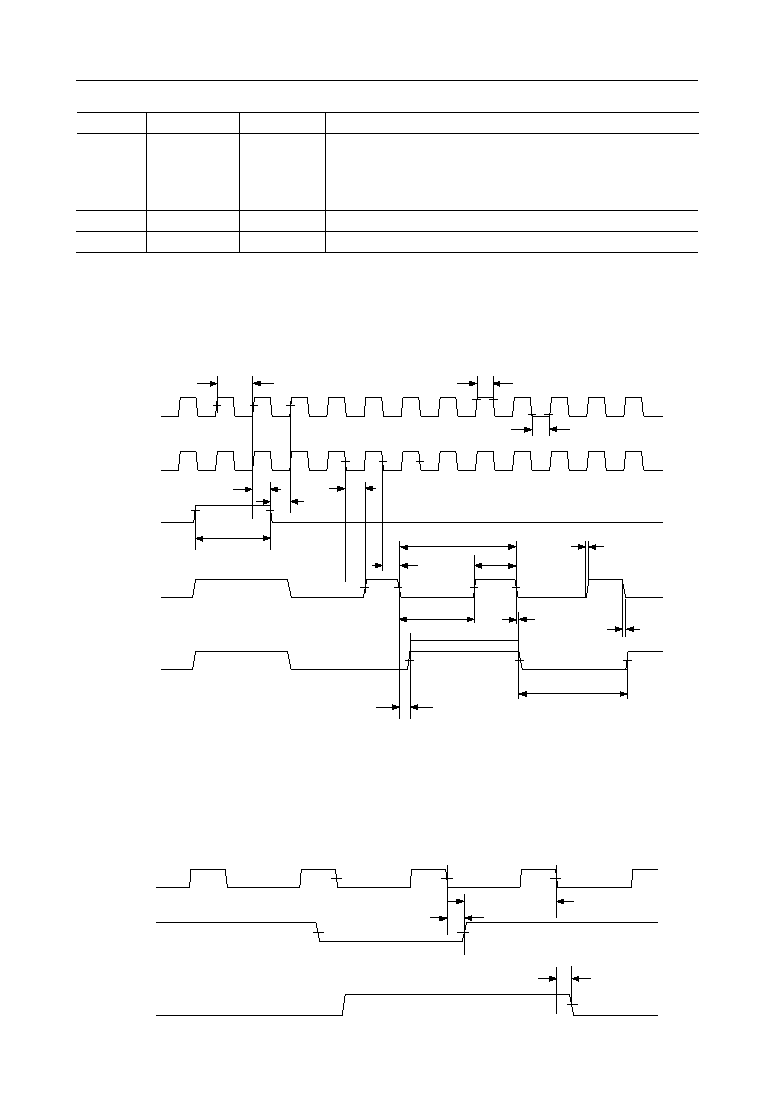
TIMING DIAGRAM
CLK ∑ PCLK ∑ OSC Waveforms
EFI
t
ELEL
t
EHEL
t
ELEH
t
EHYL
t
OLCH
t
YHEH
t
YHYL
t
CLCL
t
OLCL
t
CHCL
t
CH1CH2
t
CL2CL1
t
CLPL
t
CLCH
t
PHPL
t
CLPH
t
PLPH
OSC
CSYNC
CLK
PCLK
CLK
RES
RESET
t
CLI1H
t
I1HCL
t
CLIL
RESET Waveform
8/18
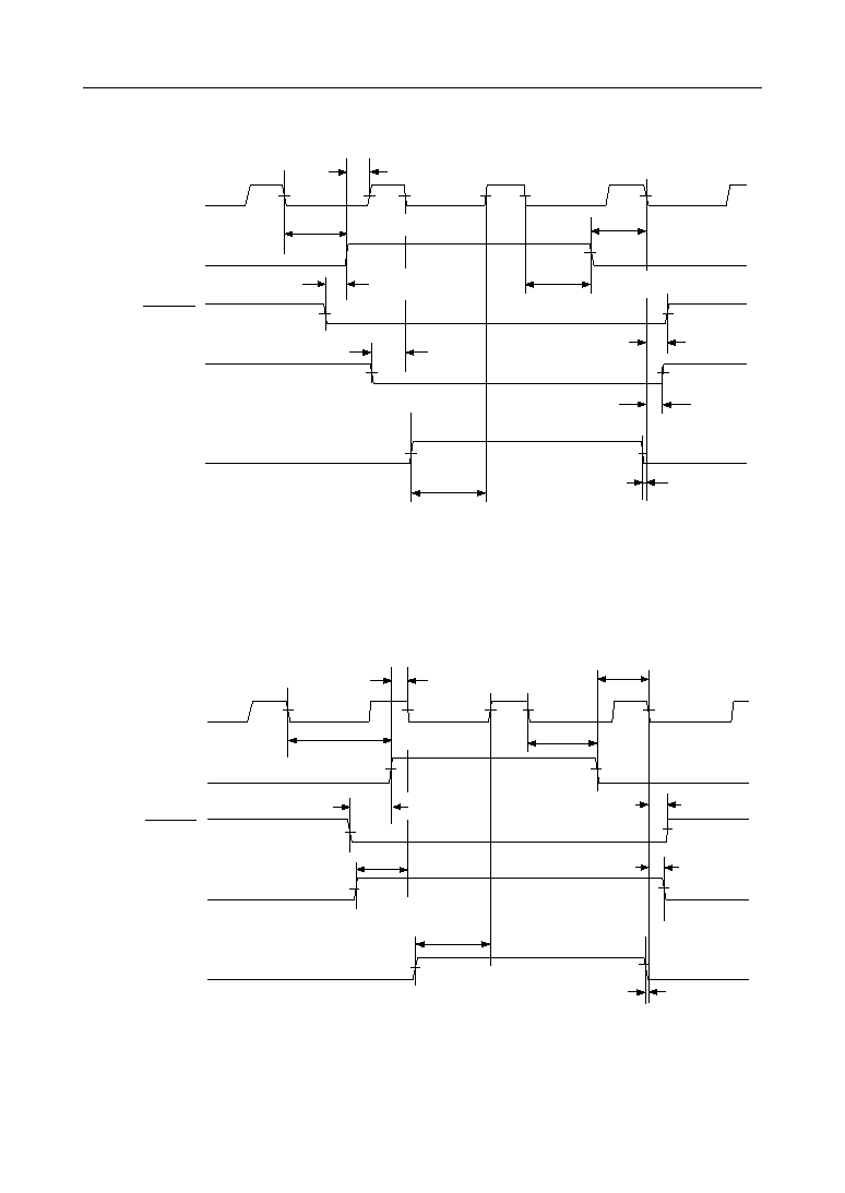
° Semiconductor
MSM82C84A-2RS/GS/JS
READY Waveform (ASYNC = L)
CLK
t
R1VCH
t
CLR1X
t
R1VCL
t
CLR1X
t
A1R1V
t
AYVCL
t
CLA1X
t
CLAYX
t
RYLCL
t
RYHCH
RDY
1
-
2
AEN
1
-
2
ASYNC
READY
t
CLR1X
t
R1VCL
t
CLR1X
t
R1VCL
t
CLA1X
t
CLAYX
t
RYLCL
t
RYHCH
t
AYVCL
t
A1R1V
CLK
RDY
1
-
2
AEN
1
-
2
ASYNC
READY
READY Waveform (ASYNC = H)
9/18
° Semiconductor
MSM82C84A-2RS/GS/JS
OPERATIONAL DESCRIPTION
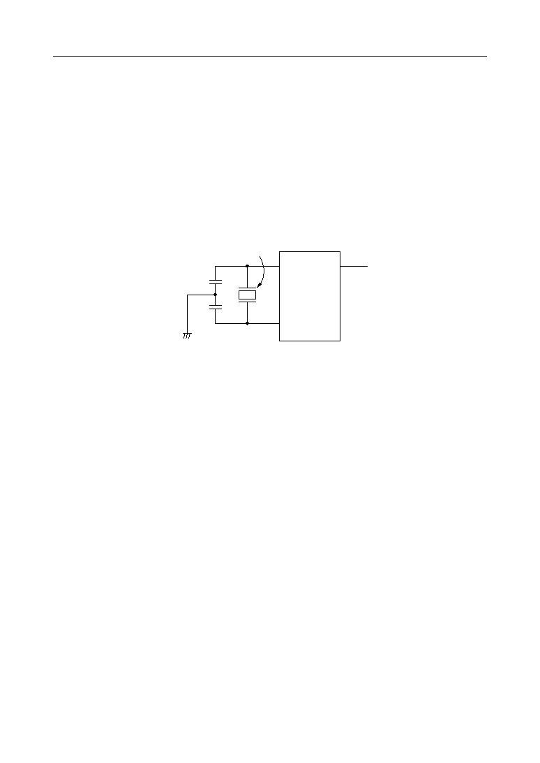
(1) Oscillator Circuit
The MSM82C84A-2 internal oscillator circuit can be driven by connecting a crystal oscillator to
the X
1
and X
2
pins.
The frequency of the crystal oscillator in this case needs to be three times greater than the desired
CLK frequency.
Since the oscillator circuit output (the same output as for the crystal resonator frequency)
appears at the OSC pin, independent use of this output is also possible.
Oscillator Circuit Example
C
1
C
2
X
1
X
2
MSM
82C84A-2
OSC
Crystal Oscillator
When input frequency is 6 to 15 MHz
C
1
= C
2
= 33 pF
When input frequency is 15 to 24 MHz
C
1
= C
2
= 10 pF
Note: Because Oscillator circuit and values depend on crystal oscillator characteristics,
OKI recommends to make contact with crystal oscillator vendor to determine
the best circuit and values for customers' application.
(2) Clock Generator Circuit
This circuit generates two clock outputs-CLK obtained by dividing the input external clock or
crystal oscillator circuit output by three, and PCLK obtained by halving CLK. CLK and PCLK
are generated from the external clock applied to the EFI pin when F/C is at high level, and are
generated from the crystal oscillator circuit when at low level.
(3) Reset Circuit
Since a Schmitt trigger circuit is used in the RES input, the MSM82C84A-2 can be reset by "power
on" by connection to a simple RC circuit. If the MSM80C86A-10 or MSM80C88A-10 is used as
the CPU in this case, it is necessary to keep the RES input at low level for at least 50 ms after Vcc
reaches the 4.5V level.
10/18
° Semiconductor
MSM82C84A-2RS/GS/JS
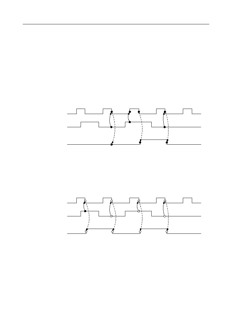
(4) Ready Circuit
The READY signal generator circuit can be set to synchronization mode by ASYNC.
(i)
When ASYNC is at low level
The RDY input is output as the READY signal by double synchronization.
The high-level RDY input is synchronized once by the rising edge of the CLK of the first
stage flip-flop (F1 in the circuit diagram), and then synchronized again by the falling
edge of the CLK of the next stage flip-flop (F2 in the circuit diagram), resulting in output
of a high-level READY output signal (see diagram below).
The low-level RDY input is synchronized directly by the falling-edge of the CLK of the
next stage flip-flop, resulting in output of a low-level READY output signal (see
diagram below).
(ii) When ASYNC is at high level
The RDY input is output as the READY signal by single synchronization.
Both low-level and high-level RDY inputs are synchronized by the falling edge of the
CLK of the next stage flip-flop, resulting output of respective low-level and high-level
READY output signals (see diagram below).
CLK
RDY
READY
CLK
RDY
READY
11/18
° Semiconductor
MSM82C84A-2RS/GS/JS
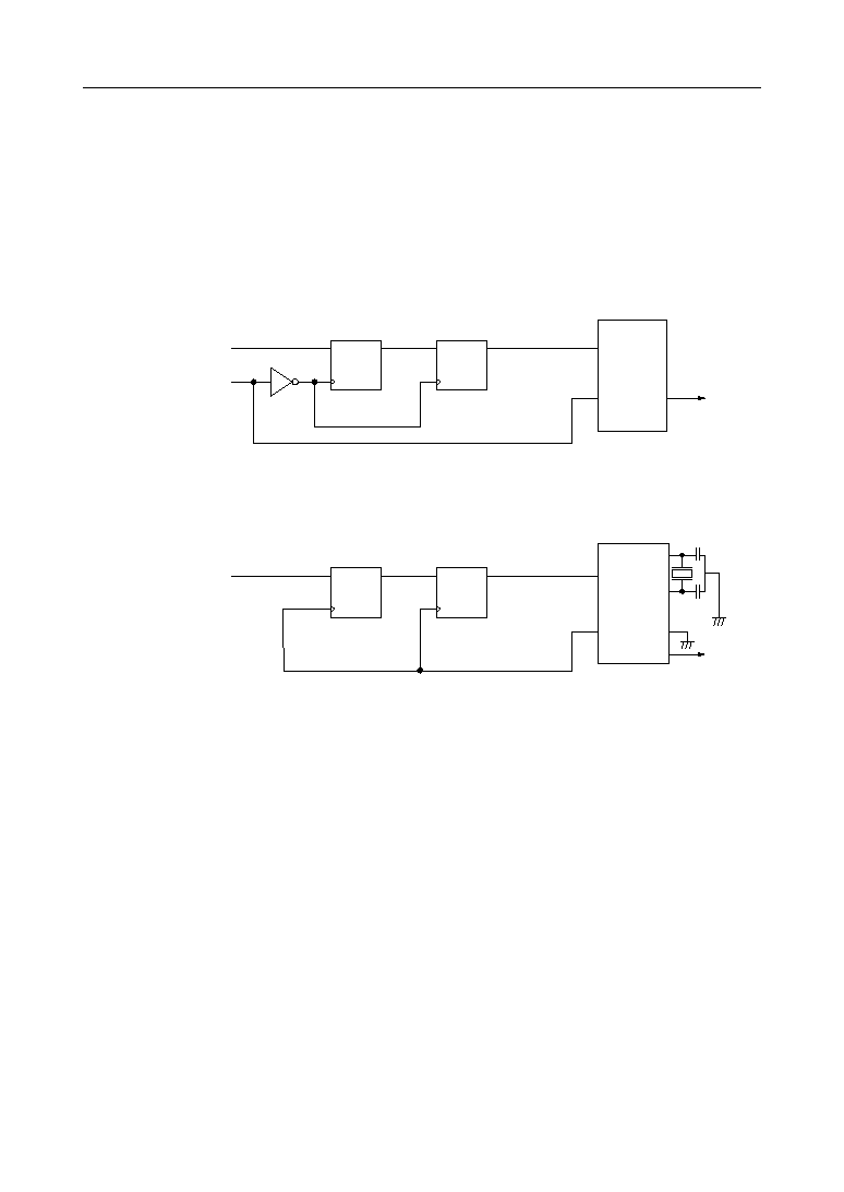
EXAMPLE OF USE (CSYNC)
The MSM82C84A-2 1/3 frequency divider counter is unsettled when the power is switched
on. Therefore, the CSYNC pin has been included to synchronize CLK with another signal.
When CSYNC is at high level, both CLK and PCLK are high-level outputs. If CSYNC is then
switched to low level, CLK is output from the next input clock rising edge, and is divided
by 3.
If CSYNC has not been synchronized with the input clock, use the following circuit to
achieve the required synchronization
External Sychronizing
Signal
D
CK
Q
D
CKÿ
Q
EFI
CLK
CLK
CSYNC
MSM
82C84A-2
External Clock
Signal (EFI)
When an external clock EFI is used as the clock source
External Sychronizing
Signal
D
CK
Q
D
CKÿ
Q
OSC
CLK
F/C
CSYNC
MSM
82C84A-2
When the crystal oscillator is used as the clock source
CLK
X
1
X
2
NOTES ON USE
The MSM82C84A-2 cannot be used if the MSM80C86A-10 or MSM80C88A-10 is used within the
range of 8 MHz < operating frequency £ 10 MHz.

12/18
° Semiconductor
MSM82C84A-2RS/GS/JS
NOTICE ON REPLACING LOW-SPEED DEVICES WITH HIGH-SPEED DEVICES
The conventional low speed devices are replaced by high-speed devices as shown below.
When you want to replace your low speed devices with high-speed devices, read the replacement
notice given on the next pages.
High-speed device (New)
Low-speed device (Old)
Remarks
M80C85AH
M80C85A/M80C85A-2
8bit MPU
M80C86A-10
M80C86A/M80C86A-2
16bit MPU
M80C88A-10
M80C88A/M80C88A-2
8bit MPU
M82C84A-2
M82C84A/M82C84A-5
Clock generator
M81C55-5
M81C55
RAM.I/O, timer
M82C37B-5
M82C37A/M82C37A-5
DMA controller
M82C51A-2
M82C51A
USART
M82C53-2
M82C53-5
Timer
M82C55A-2
M82C55A-5
PPI
13/18
° Semiconductor
MSM82C84A-2RS/GS/JS
Differences between MSM82C84A and MSM82C84A-5/MSM82C84A-2
1) Manufacturing Process
All these devices use a 3 m Si-Gate CMOS process technology.
The chip size of these devices is same.
The chip of the MSM82C84A-5 is entirely identical to that of the MSM82C84A-2.
2) Functions
3) Electrical Characteristics
3-1) DC Characteristics
As shown above, the MSM82C84A-5/MSM82C84A-2 satisfies the characteristics (except for V
OL
and input current (ASYNC) of the MSM82C84A.
Item
MSM82C84A
MSM82C84A-5/-2
Internal processing of ASYNC pin
Normal CMOS input pin
Input pin with built-in pull up resistor
Notes on use
The pin should have a pullup or
pulldown resistor if it is unused.
The value of pulldown resistor
(when used) is limited. (See page 3.)
Parameter
Symbol
MSM82C84A
MSM82C84A-5/-2
''L''Level Output Voltage (CLK)
0.45 V maximum (+5 mA)
0.40 V maximum (+4 mA)
''L''Level Output Voltage
(Other than CLK)
0.45 V maximum (+5 mA)
0.40 V maximum (+2.5 mA)
V
OL
V
OL
V
OH
V
OH
V
IHR-
V
ILR
I
LIA
I
LI
I
CCS
''H''Level Output Voltage (CLK)
3.7 V minimum (-1 mA)
V
CC
-0.1 V minimum (-4 mA)
''H''Level Output Voltage
(Other than CLK)
3.7 V minimum (-1 mA)
V
CC-
0.1 V minimum (-1 mA)
RES Input Hysteresis Width
0.25 V minimum
0.2 • V
CC
min
Input Current (ASYNC)
-10 mA to +10 mA
-100 mA~+10 mA
Input Leak Current
-10 mA to +10 mA
-1 mA~+1 mA
Supply Current (Standby)
100 mA maximum
40 mA maximum
14/18
° Semiconductor
MSM82C84A-2RS/GS/JS
3-2) AC Charasteristics
1) MSM82C84A and MSM82C84A-2
As shown above, the MSM82C84A-2 satisfies the characteristics (except for Input Rise/Fall Time)
of the MSM82C84A.
1) MSM82C84A-5 and MSM82C84A-2
As shown above, the MSM82C84A-2 satisfies the characteristics of the MSM82C84A-5.
Parameter
Symbol
MSM82C84A-5
MSM82C84A-2
EFI High Time
20 ns minimum
13 ns minimum
EFI Low Time
20 ns minimum
17 ns minimum
t
EHEL
t
ELEH
--
t
CHCL
Crystal Frequency
15 MHz maximum
24 MHz maximum
CLK Period
200 ns minimum
125 ns minimum
EFI Period
t
ELEL
66 ns minimum
36 ns minimum
Parameter
Symbol
MSM82C84A
MSM82C84A-2
Input Rise Time
20 ns maximum
15 ns maximum
Input Fall Time
20 ns maximum
15 ns maximum
t
ILIH
t
ILIH
t
CLCH
t
CH1CH2
t
PHPL
t
RYHCH
CLK Low Time
119 ns minimum
2/3 t
CLCL
-15 ns minimum
CLK Rise/Fall Time
15 ns maximum
10 ns maximum
PCLK High Time
180 ns minimum
t
CLCL
-20 ns minimum
READY Falling to CLK Rising
114 ns minimum
2/3 t
CLCL
-15 ns minimum
t
PLPH
PCLK Low Time
180 ns minimum
t
CLCL
-20 ns minimum
CLK High Time
t
CHCL
t
CL1CL2
65 ns minimum
1/3 t
CLCL
+2 ns minimum

15/18
° Semiconductor
MSM82C84A-2RS/GS/JS
4) Notices on use
Note the following when replacing devices as the ASYNC pin is differently treated between the
MSM82C84A and the MSM82C84A-5/MSM82C84A-2:
Case 1: When only a pullup resistor is externally connected to.
The MSM82C84A can be replaced by the MSM82C84A-2.
Case 2: When only pulldown resistor is externally connected to.
When the pulldown resistor is 8 kiloohms or less, the MSM82C84A can be replaced by the
MSM82C84A-2.
When the pulldown resistor is greater than 8 kiloohms, use a pulldown resistor of 8 kiloohms or less.
Case 3: When an output of the other IC device is connected to the device.
The MSM82C84A can be replaced by the MSM82C84A-2 when the I
OL
pin of the device to drive the
ASYNC pin of the MSM82C84A-2 has an allowance of 100 mA or more.
16/18
° Semiconductor
MSM82C84A-2RS/GS/JS
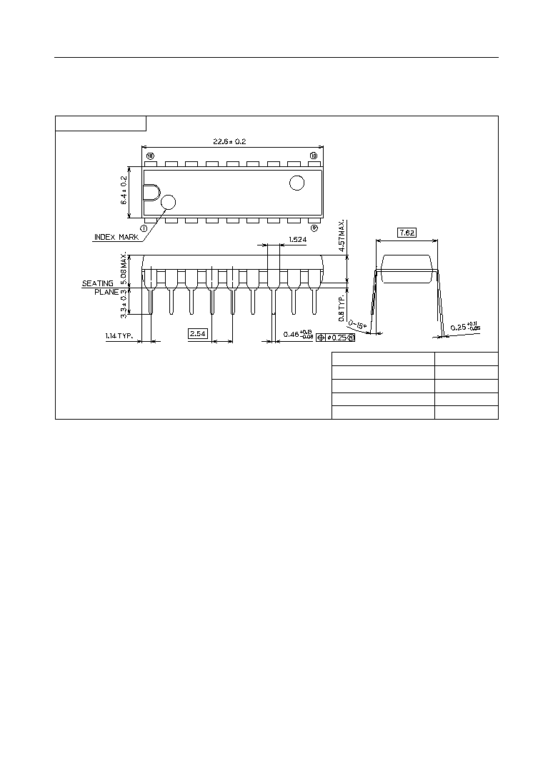
(Unit : mm)
PACKAGE DIMENSIONS
Notes for Mounting the Surface Mount Type Package
The SOP, QFP, TSOP, SOJ, QFJ (PLCC), SHP and BGA are surface mount type packages, which
are very susceptible to heat in reflow mounting and humidity absorbed in storage.
Therefore, before you perform reflow mounting, contact Oki's responsible sales person for the
product name, package name, pin number, package code and desired mounting conditions
(reflow method, temperature and times).
DIP18-P-300-2.54
Package material
Lead frame material
Pin treatment
Solder plate thickness
Package weight (g)
Epoxy resin
42 alloy
Solder plating
5 mm or more
1.30 TYP.
17/18
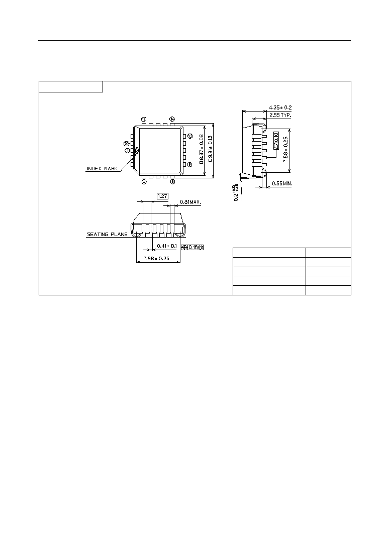
° Semiconductor
MSM82C84A-2RS/GS/JS
(Unit : mm)
Notes for Mounting the Surface Mount Type Package
The SOP, QFP, TSOP, SOJ, QFJ (PLCC), SHP and BGA are surface mount type packages, which
are very susceptible to heat in reflow mounting and humidity absorbed in storage.
Therefore, before you perform reflow mounting, contact Oki's responsible sales person for the
product name, package name, pin number, package code and desired mounting conditions
(reflow method, temperature and times).
QFJ20-P-S350-1.27
Package material
Lead frame material
Pin treatment
Solder plate thickness
Package weight (g)
Epoxy resin
Cu alloy
Solder plating
5 mm or more
0.59 TYP.
Spherical surface
18/18
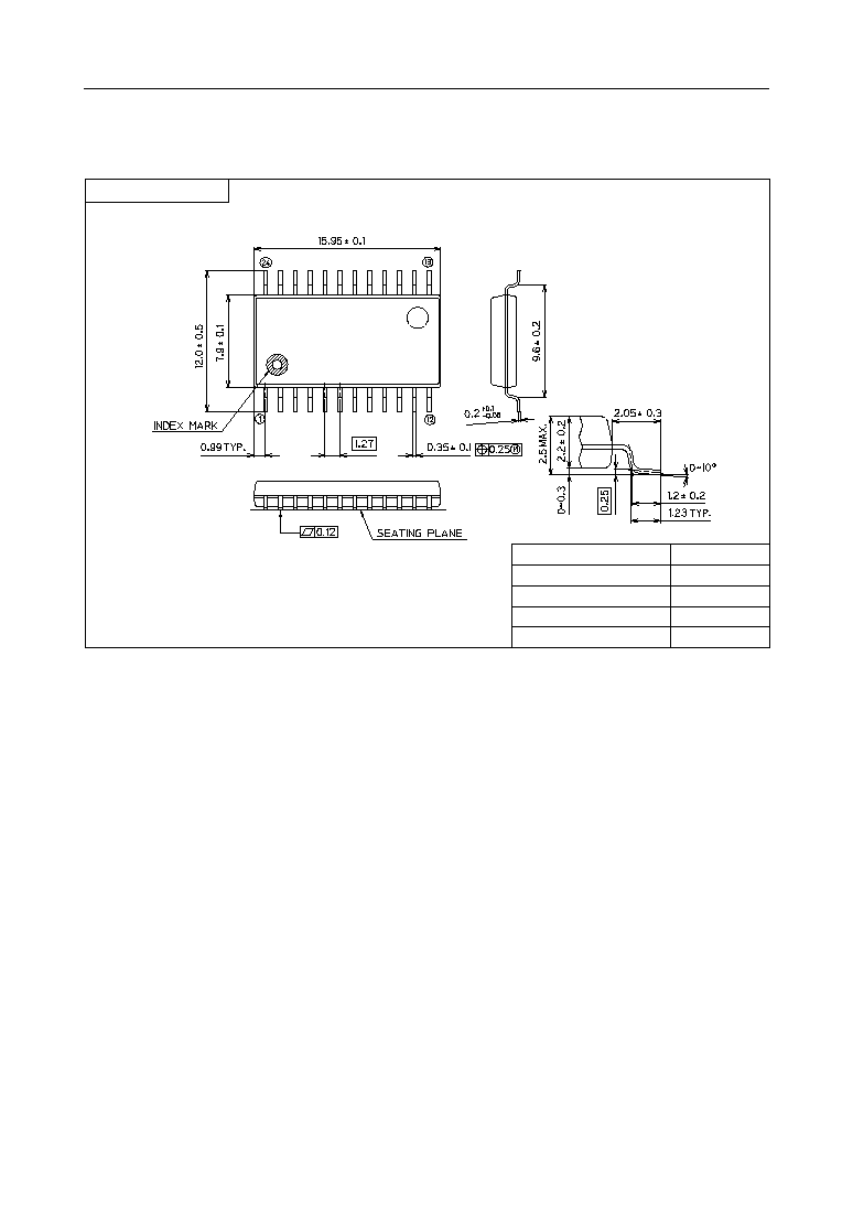
° Semiconductor
MSM82C84A-2RS/GS/JS
(Unit : mm)
Notes for Mounting the Surface Mount Type Package
The SOP, QFP, TSOP, SOJ, QFJ (PLCC), SHP and BGA are surface mount type packages, which
are very susceptible to heat in reflow mounting and humidity absorbed in storage.
Therefore, before you perform reflow mounting, contact Oki's responsible sales person for the
product name, package name, pin number, package code and desired mounting conditions
(reflow method, temperature and times).
SOP24-P-430-1.27-K
Package material
Lead frame material
Pin treatment
Solder plate thickness
Package weight (g)
Epoxy resin
42 alloy
Solder plating
5 mm or more
0.58 TYP.
Mirror finish