
° Semiconductor
MSM9210
1/20
FEDL9210-04
GENERAL DESCRIPTION
The MSM9210 is a full CMOS controller/driver for Duplex or Triplex (1/2 duty or 1/3 duty)
vacuum fluorescent display tube. It consists of a 32-segment driver multiplexed to drive up to
96 segments, and 10-bit digital dimming circuit.
MSM9210 features a selection of a master mode and a slave mode, and therefore it can be used
to expand segments for the VFD driver with keyscan and A/D converter function.
MSM9210 provides an interface with a microcontroller only by three signal lines: DATA IN,
CLOCK and CS.
FEATURES
∑ Logic supply voltage (V
DD
)
: 4.5 to 5.5V
∑ Driver supply voltage (V
DISP
)
: 8 to 18V
∑ Duplex/Triplex (1/2 duty / 1/3 duty) selectable
DUP/TRI=1/2 duty selectable at "H" level
DUP/TRI=1/3 duty selectable at "L" level
∑ Number of display segments
Max. 64-segment display (during 1/2 duty mode)
Max. 96-segment display (during 1/3 duty mode)
∑ Master/Slave selectable
M/S=Master mode selectable at "H" level
M/S=Slave mode selectable at "L" level
∑ Interface with a microcontroller
Three lines: CS, CLOCK, and DATA IN
∑ 32-segment driver outputs
: I
OH
=≠5mA at V
OH
=V
DISP
≠0.8V (SEG1 to 22)
(can be directly connected to VFD tube
: I
OH
=≠10mA at V
OH
=V
DISP
≠0.8V (SEG23 to 32)
and require no external resisters)
: I
OL
=500mA at V
OL
=2V (SEG1 to 32)
∑ 3-grid pre-driver outputs
: I
OH
=≠5.0mA at V
OH
=V
DISP
≠0.8V
(require external drivers)
I
OL
=10mA at V
OL
=2V
∑ Logic outputs
: I
OH
=≠200mA at V
OH
=V
DD
≠0.8V
I
OL
=200mA at V
OL
=0.8V
∑ Built-in digital dimming circuit (10-bit resolution)
∑ Built-in oscillation circuit (external R and C)
∑ Built-in Power-On-Reset circuit
∑ Package options:
56-pin plastic QFP (QFP56-P-910-0.65-2K)
Product name: MSM9210GS-2K
64-pin plastic QFP (QFP64-P-1414-0.80-BK)
Product name: MSM9210GS-BK
° Semiconductor
MSM9210
32-Bit Duplex/Triplex (1/2 duty / 1/3 duty) VF Controller/Driver with Digital Dimming
FEDL9210-04
This version: May 2000
Previous version: Set. 1999
° Semiconductor
MSM9210
2/20
FEDL9210-04
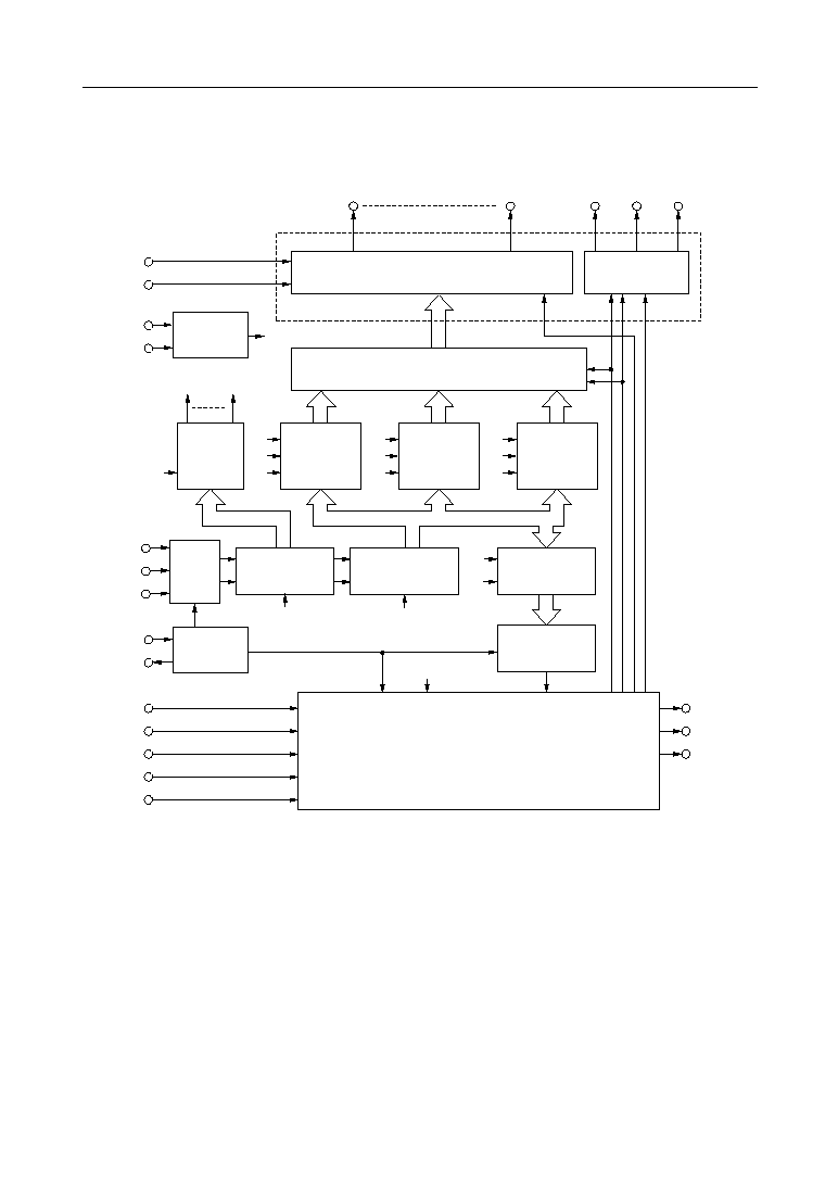
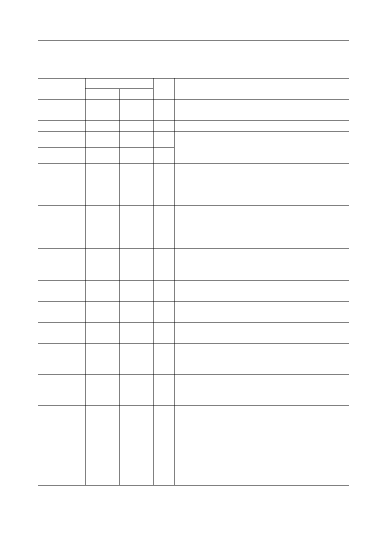
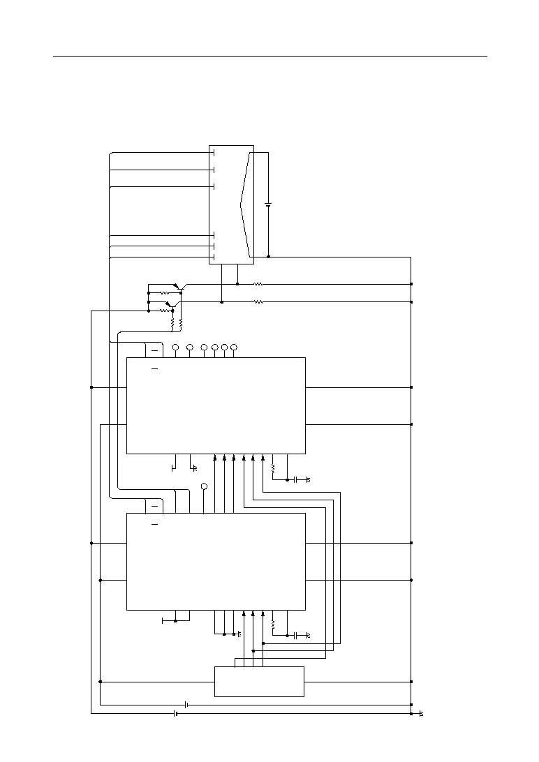
BLOCK DIAGRAM
Timing Generator
DIM OUT
SYNC OUT1
SYNC OUT2
DIM IN
SYNC IN1
SYNC IN2
M/S
DUP/TRI
OSC
Control
Out1-32
32bit Shift Register
in1-10
Dimming Latch
Out1-10
10bit Digital
Dimming
POR
OSC0
OSC1
CS
CLOCK
DATA IN
Out1-3
3bit Shift Register
POR
POR
POR
4H
Out1-32
Segment Latch
3
in1-32
0H
3H
POR
Out1-32
Segment Latch
2
in1-32
0H
2H
POR
Out1-32
Segment Latch
1
in1-32
0H
1H
POR
Mode Select
in1-3
POR
0H
4H
Power
On
Reset
V
DD
L-GND
POR
Out1-32
96 to 32 Segment Control
in1-32
in1-32
in1-32
in1-32
32 Segment Driver
V
DISP
D-GND
3 Grid pre Driver
GRID2 GRID3
GRID1
SEG32
SEG1
° Semiconductor
MSM9210
3/20
FEDL9210-04
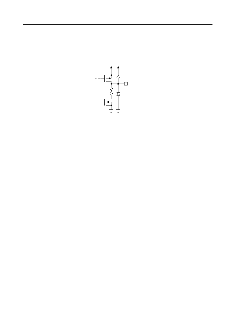
INPUT AND OUTPUT CONFIGURATION
Schematic Diagram of Driver Output Circuit
V
DISP
OUTPUT
D-GND
D-GND
V
DISP
° Semiconductor
MSM9210
4/20
FEDL9210-04
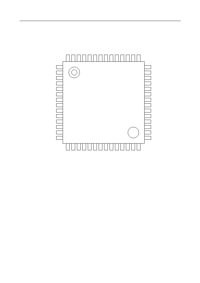
PIN CONFIGURATION (TOP VIEW)
42
41
40
39
38
37
36
35
34
33
32
1
2
3
4
5
6
7
8
9
10
11
SEG25
SEG26
SEG27
SEG28
SEG29
SEG30
SEG31
SEG32
GRID1
GRID2
GRID3
SEG13
SEG12
SEG11
SEG10
SEG9
SEG8
SEG7
SEG6
SEG5
SEG4
SEG3
56
55
54
53
52
51
50
49
48
V
DISP
SEG24
SEG23
SEG22
SEG21
SEG20
SEG19
D-GND
SEG18
15
16
17
18
19
20
21
22
23
DIM IN
SYNC IN 1
SYNC IN 2
CS
CLOCK
DATA IN
L-GND
OSC1
OSC0
12
D-GND
13
NC
14
V
DD
24
DUP/
TRI
25
M/
S
26
SYNC OUT 2
27
SYNC OUT 1
28
DIM OUT
31 SEG2
30 SEG1
29 NC
47
SEG17
46
SEG16
45
SEG15
44
SEG14
43
V
DISP
NC: No connection
56-pin Plastic QFP
° Semiconductor
MSM9210
5/20
FEDL9210-04
NC: No connection
64-pin Plastic QFP
48
47
46
45
44
43
42
41
40
39
38
1
2
3
4
5
6
7
8
9
10
11
NC
SEG25
SEG26
SEG27
SEG28
SEG29
SEG30
SEG31
SEG32
GRID1
GRID2
NC
NC
SEG13
SEG12
SEG11
SEG10
SEG9
SEG8
SEG7
SEG6
SEG5
64
63
62
61
60
59
58
57
56
55
54
V
DISP
NC
SEG24
SEG23
SEG22
SEG21
SEG20
SEG19
D-GND
SEG18
SEG17
17
18
19
20
21
22
23
24
25
26
27
NC
DIM IN
SYNC IN1
SYNC IN2
CS
CLOCK
DATA IN
L-GND
OSC1
OSC0
DUP/
TRI
12
GRID3
13
D-GND
14
NC
15
V
DD
16
NC
28
M/
S
29
SYNC OUT2
30
SYNC OUT1
31
DIM OUT
32
NC
37 SEG4
36 SEG3
35 SEG2
34 SEG1
33 NC
53
SEG16
52
SEG15
51
SEG14
50
NC
49
V
DISP
° Semiconductor
MSM9210
6/20
FEDL9210-04
PIN DESCRIPTIONS
Symbol
QFP56
Type
Description
V
DISP
43,56
--
Power supply pins for VFD driver circuit.
43 pin and 56 pin should be connected externally.
V
DD
14
--
Power supply pin for logic drive.
D-GND
12, 49
--
L-GND
21
--
SEG1 to 22
30 to 42,
44 to 48,
50 to 53
O
D-GND is ground pin for the VFD driver circuit. L-GND is ground
pin for the logic circuit. 12pin, 21pin and 49pin should be
connected externally.
Segment (anode) signal output pins for a VFD tube.
These pins can be directly connected to the VFD tube.
External circuit is not required.
IOH£≠5 mA
SEG23 to 32
1 to 8,
54, 55
O
Segment (anode) signal output pins for a VFD tube.
These pins can be directly connected to the VFD tube.
External circuit is not required.
IOH£≠10 mA
GRID1 to 3
9, 10, 11
O
Inverted Grid signal output pins.
For pre-driver, the external circuit is required.
IOL£10 mA
CS
18
I
Chip select input pin.
Data is not transferred when CS is set to a Low level.
CLOCK
19
I
Shift clock input pin.
Serial data shifts at the rising edge of the CLOCK.
DATA IN
20
I
Serial data input pin (positive logic).
Data is input to the shift register at the rising edge of the CLOCK signal.
DUP/TRI
24
I
Duplex/Triplex operation select input pin.
Duplex (1/2 duty) operation is selected when this pin is set to V
DD
.
Triplex (1/3 duty) operation is selected when this pin is set to L-GND.
M/S
25
I
Master/Slave mode select input pin.
Master mode is selected when this pin is set to V
DD
.
Slave mode is selected when this pin is set to L-GND.
Dimming pulse input.
When the slave mode is selected, the pulse width of the all segment
output are controlled by a input pulse width of DIM IN.
Connect this pin to the master side DIM OUT pin at the slave mode.
When the master mode is selected, the input level of this pin is
ignored and the pulse width of the all grids and segment outputs are
controlled by a built-in 10-bit dimming circuit.
Connect this pin to V
DD
or L-GND at the master mode.
DIM IN
15
I
QFP64
49,64
15
13, 56
24
34 to 46,
51 to 55,
57 to 60
2 to 9,
61, 62
10, 11, 12
21
22
23
27
28
18
Pin
° Semiconductor
MSM9210
7/20
FEDL9210-04
Symbol
QFP56
Type
Description
SYNC OUT 1, 2
26, 27
O
Synchronous signal output.
Connect these pins to the slave side SYNC IN 1, and 2 pins.
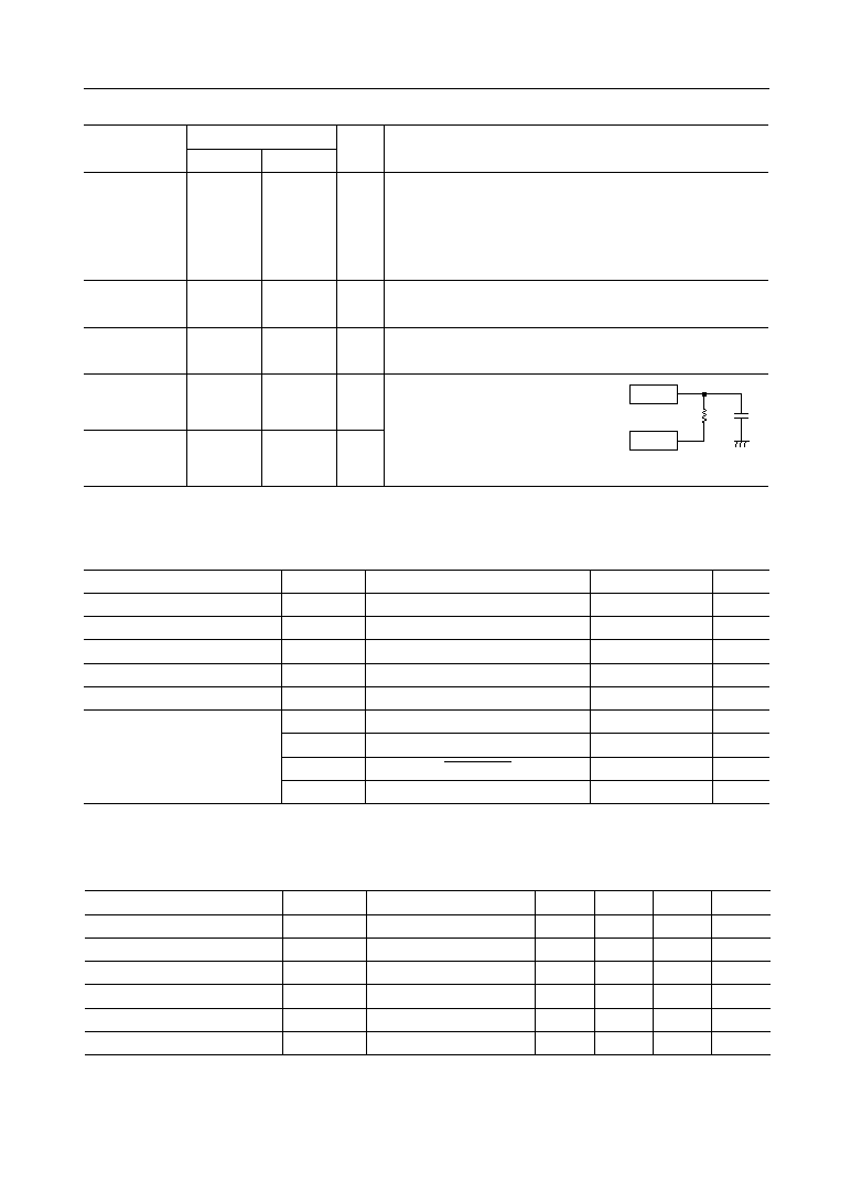
OSC0
23
I
OSC1
22
O
RC oscillator connecting pins.
Oscillation frequency depends on
display tubes to be used.
For details, refer to ELECTRICAL
CHARACTERISTICS.
OSC0
OSC1
R
C
QFP64
29, 30
26
25
Pin
SYNC IN 1, 2
16, 17
I
Synchronous signal input.
When the slave mode is selected, connect these pins to the master
side SYNC OUT 1, and 2 pins.
When the master mode is selected, the input level of these pins are ignored.
Connect these pins to V
DD
or L-GND at the master mode.
DIM OUT
28
O
Dimming pulse output.
Connect this pin to the slave side DIM IN pin.
19, 20
31
ABSOLUTE MAXIMUM RATING
RECOMMENDED OPERATING CONDITIONS
Parameter
Symbol
V
DISP
Driver Supply Voltage
V
DD
Logic Supply Voltage
V
IH
High Level Input Voltage
V
IL
Low Level Input Voltage
f
C
Clock Frequency
T
OP
Operating Temperature
Condition
Min.
Typ.
Max.
Unit
--
8.0
13.0
18.0
V
--
4.5
5.0
5.5
V
All inputs except OSC0
0.8V
DD
--
--
V
All inputs except OSC0
--
--
0.2V
DD
V
--
--
--
1.0
MHz
--
≠40
--
+85
∞C
Parameter
Symbol
Condition
Ratings
Unit
V
DISP
--
≠0.3 to +20
V
Driver Supply Voltage
V
DD
--
V
Logic Supply Voltage
V
IN
--
V
Input Voltage
P
D
Ta25
∞
C
mW
Power Dissipation
T
STG
--
∞
C
Storage Temperature
I
O1
SEG1 to 22
mA
I
O2
SEG23 to 32
mA
Output Current
I
O3
GRID1 to 3
mA
I
O4
DIM OUT, SYNC OUT1, SYNC OUT2
mA
≠0.3 to +6.5
≠0.3 to V
DD
+0.3
260
≠55 to +150
≠10.0 to +2.0
≠20.0 to +2.0
≠10.0 to +20.0
≠2.0 to +2.0
° Semiconductor
MSM9210
8/20
FEDL9210-04
When a 1/2 duty VFD tube is used
When a 1/3 duty VFD tube is used
Parameter
Symbol
f
OSC
Oscillation Frequency
f
FR
Frame Frequency
Condition
Min.
Typ.
Max.
Unit
R=8.2KW±5%, C=22pF±5%
1.0
1.5
2.0
MHz
R=8.2KW±5%, C=22pF±5%
122
183
244
Hz
Parameter
Symbol
f
OSC
Oscillation Frequency
f
FR
Frame Frequency
Condition
Min.
Typ.
Max.
Unit
R=6.2KW±5%, C=22pF±5%
1.5
2.25
3.0
MHz
R=6.2KW±5%, C=22pF±5%
122
183
244
Hz
° Semiconductor
MSM9210
9/20
FEDL9210-04
ELECTRICAL CHARACTERISTICS
DC Characteristics
Parameter
Symbol
V
IH
High Level Input Voltage
V
IL
Low Level Input Voltage
I
IH
High Level Input Current
I
IL
Low Level Input Current
V
OH1
V
OH2
V
OH3
High Level Output Voltage
Condition
Min.
Max.
Unit
--
0.8V
DD
--
V
--
--
0.2V
DD
V
V
IH
=V
DD
≠1.0
+1.0
m
A
V
IL
=GND
≠1.0
+1.0
m
A
V
DISP
≠0.8
--
V
V
DISP
≠0.8
--
V
V
DISP
≠0.8
--
V
V
DD
≠0.8
--
V
V
DISP
=9.5V
Applied pin
*1)
*1)
*1)
*1)
SEG1-22
SEG23-32
GRID1-3
V
OH4
*2)
V
DD
=4.5V
I
OH1
=≠5mA
I
OH2
=≠10mA
I
OH3
=≠5mA
I
OH4
=≠200mA
V
OL1
V
OL2
V
OL3
Low Level Output Voltage
--
2.0
V
--
2.0
V
--
2.0
V
--
0.8
V
V
DISP
=9.5V
SEG1-22
SEG23-32
GRID1-3
V
OL4
*2)
V
DD
=4.5V
I
OL1
=500mA
I
OL2
=500mA
I
OL3
=10mA
I
OL4
=200mA
--
5.0
mA
I
DD
V
DD
Supply Current
--
100
m
A
I
DISP
V
DISP
f
OSC
=3.0MHz, no load
f
OSC
=3.0MHz, no load
Ta=≠40 to +85∞C,V
DISP
=8.0 to 18.0V, V
DD
=4.5 to 5.5V
*1) CS, CLOCK, DATA IN, DIM IN, SYNC IN 1, SYNC IN 2, M/S, DUP/TRI
*2) DIM OUT, SYNC OUT 1, SYNC OUT 2
° Semiconductor
MSM9210
10/20
FEDL9210-04
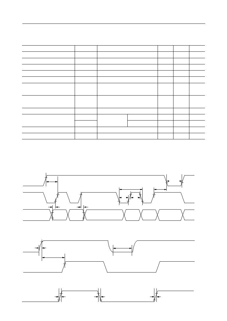
AC Characteristics
TIMING DIAGRAM
l
Data Input Timing
≠0.8V
DD
≠0.2V
DD
≠0.8V
DD
≠0.2V
DD
≠0.8V
DD
≠0.2V
DD
CS
CLOCK
DATA IN
t
DS
t
DH
t
CSS
1/f
C
t
CW
t
CW
t
CSH
t
CSL
VALID
VALID
VALID
VALID
l
Reset Timing
t
POF
t
PRZ
V
DD
CS
t
RSOFF
≠0.8V
DD
≠0.0V
≠0.8V
DD
≠0.0V
l
Driver Output Timing
≠0.8V
DISP
≠0.2V
DISP
SEG1-32, GRID1-3
t
R
t
R
t
F
Parameter
Symbol
f
C
Clock Frequency
t
CW
Clock Pulse Width
t
DS
Data Setup Time
t
DH
Data Hold Time
t
CSL
CS Off Time
t
CSS
t
R
t
PRZ
CS Setup Time
(CS-Clock)
Output Slew Rate Time
V
DD
Rise Time
Condition
Min.
Max.
Unit
--
--
1.0
MHz
--
400
--
ns
--
400
--
ns
--
400
--
ns
--
20
--
m
s
--
400
--
ns
t
R
=20% to 80%
--
2.0
m
s
t
F
=80% to 20%
--
2.0
m
s
Mounted in a unit
--
100
m
s
C
L
=100pF
t
CSH
CS Hold Time
(Clock-CS)
--
400
--
ns
t
POF
V
DD
Off Time
Mounted in a unit, V
DD
=0.0V
5.0
--
ms
t
RSOFF
CS Wait Time
--
400
--
m
s
t
F
Ta=≠40 to +85∞C,V
DISP
=8.0 to 18.0V, V
DD
=4.5 to 5.5V
° Semiconductor
MSM9210
11/20
FEDL9210-04
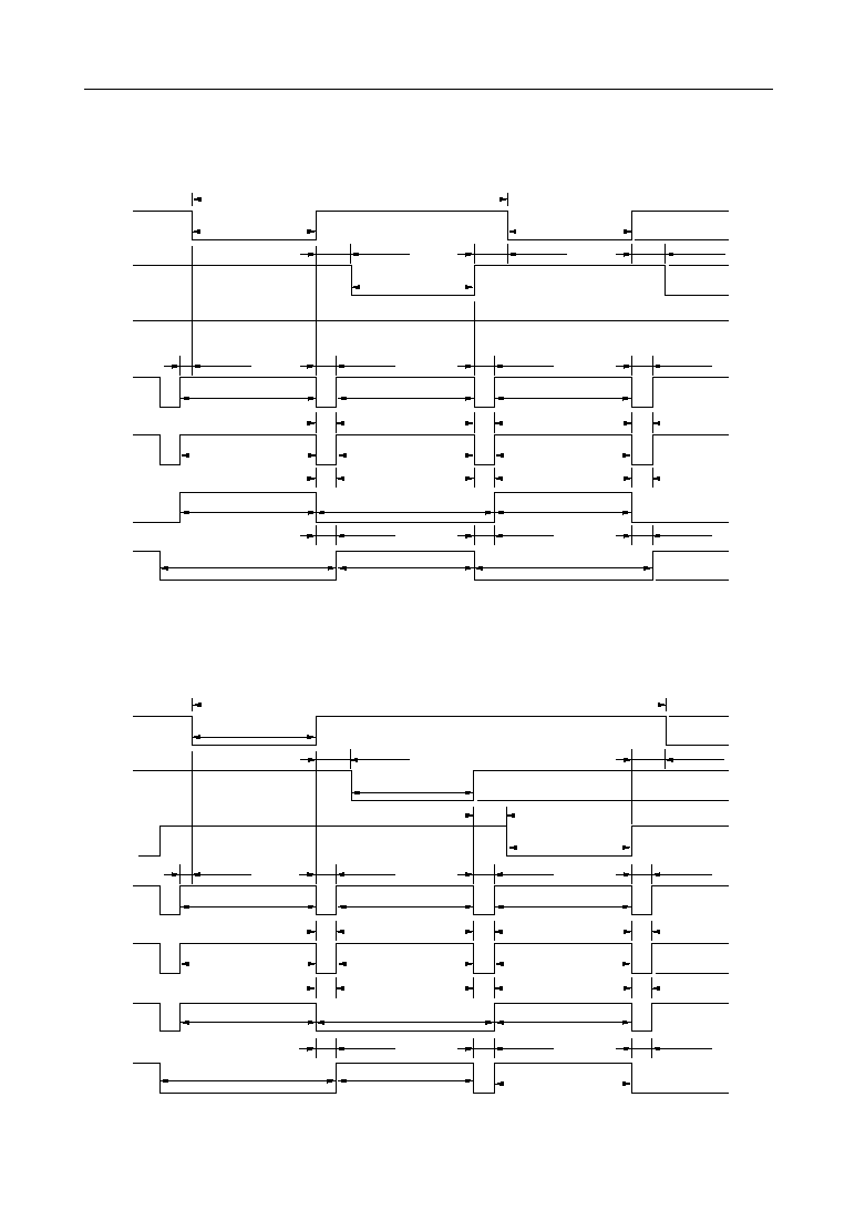
l
Output Timing (Duplex Operation)
*1bit time=4/f
OSC
(The dimming data is 1016/1024 at the master mode)
GRID1
V
DISP
D-GND
GRID2
V
DISP
D-GND
GRID3
SEG1-32
V
DISP
D-GND
DIM OUT
V
DD
L-GND
SYNC OUT1
V
DD
L-GND
SYNC OUT2
V
DD
L-GND
V
DISP
D-GND
2048bit times (1 display cycle)
1016bit times
1016bit times
1016bit times
1019bit times
1019bit times
1019bit times
1019bit times
1019bit times
1019bit times
1029bit times
1019bit times
1019bit times
1019bit times
1029bit times
1029bit times
5bit times
5bit times
5bit times
3bit times
8bit times
8bit times
8bit times
5bit times
5bit times
5bit times
5bit times
5bit times
5bit times
5bit times
5bit times
5bit times
l
Output Timing (Triplex Operation)
*1bit time=4/f
OSC
(The dimming data is 1016/1024 at the master mode)
GRID1
V
DISP
D-GND
GRID2
V
DISP
D-GND
GRID3
SEG1-32
V
DISP
D-GND
DIM OUT
V
DD
L-GND
SYNC OUT1
V
DD
L-GND
SYNC OUT2
V
DD
L-GND
V
DISP
D-GND
3072bit times (1 display cycle)
1016bit times
1016bit times
1019bit times
1019bit times
1019bit times
1019bit times
1019bit times
1019bit times
1029bit times
1019bit times
1019bit times
1019bit times
1029bit times
5bit times
5bit times
5bit times
3bit times
8bit times
8bit times
5bit times
5bit times
5bit times
5bit times
5bit times
5bit times
5bit times
5bit times
5bit times
1019bit times
1016bit times
8bit times
° Semiconductor
MSM9210
12/20
FEDL9210-04
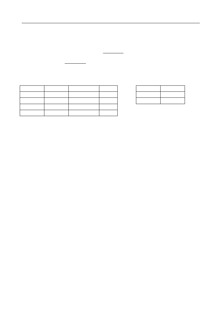
Segment Data Input [Function Mode: 0 to 3]
∑ MSM9210 receives the segment data when function mode 0 to 3 are selected.
∑ The same segment data is transferred to the 3 segment data latches corresponding to GRID 1
to 3 at the same time when the function mode 0 is selected.
∑ The segment data is transferred to only one segment data latch corresponding to the specified
GRID when the function mode is 1, 2 or 3 is selected.
∑ Segment output (SEG1 to 32) becomes High level (lightning) when the segment data (S1 to S32)
is set to "1".
[Data Format]
Input Data
: 35 bits
Segment Data : 32 bits
Mode Data
: 3 bits
FUNCTIONAL DESCRIPTION
Power-on Reset
When power is turned on, MSM9210 is initialized by the internal power-on reset circuit.
The status of the internal circuit after initialization is as follows:
∑ The contents of the shift registers and latches are set to "0".
∑ The digital dimming duty cycle is set to "0".
∑ All segment outputs are set to Low level.
∑ All grid outputs are set to High level.
Data Transfer Method
Data can be transferred between the rising edge and the next falling edge of chip select input.
The mode data, segment data and dimming data are written by a serial transfer method. The
serial data is input to the shift register at the rising edge of a shift clock pulse.
The mode data (M0 to M2) must be transferred after the segment data and dimming data
succeedingly.
When the chip select input falls, an internal LOAD signal is automatically generated and data is
loaded to the latches.
Function Mode
Function mode is selected by the mode data (M0 to M2). The relation between function mode and
mode data is as follows:
FUNCTION MODE
OPERATING MODE
FUNCTION DATA
M0
M1
M2
0
0
0
0
Segment Data for GRID1-3 Input
1
0
0
1
Segment Data for GRID1 Input
0
1
0
2
Segment Data for GRID2 Input
1
1
0
3
Segment Data for GRID3 Input
0
0
1
4
Digital Dimming Data Input
1
S1
2
S2
3
S3
4
S4
29
S29
30
S30
31
S31
32
S32
33
M0
34
M1
35
M2
Bit
Input Data
Segment Data (32bits)
Mode Data
(3bits)
° Semiconductor
MSM9210
13/20
FEDL9210-04
[Bit correspondence between segment output and segment data]
1
S1
17
S17
2
S2
18
S18
3
S3
19
S19
4
S4
20
S20
5
S5
21
S21
6
S6
22
S22
7
S7
23
S23
8
S8
24
S24
9
S9
25
S25
10
S10
26
S26
11
S11
27
S27
12
S12
28
S28
13
S13
29
S29
14
S14
30
S30
15
S15
31
S31
16
S16
32
S32
SEG n
Segment data
SEG n
Segment data
Digital Dimming Data Input [Function Mode: 4]
∑ MSM9210 receives the digital dimming data when function mode 4 is selected.
∑ The output duty changes in the range of 0/1024 (0%) to 1016/1024 (99.2%) for each grid.
∑ The 10-bit digital dimming data is input from LSB.
[Data Format]
Input Data
: 13 bits
Digital Dimming Data: 10 bits
Mode Data
: 3 bits
1
D1
2
D2
3
D3
4
D4
7
D7
8
D8
9
D9
10
D10
11
M0
12
M1
13
M2
Bit
Input Data
Digital Dimming Data (10bits)
Mode Data
(3bits)
5
D5
6
D6
D10
0
0
1
1
1
1
D9
0
0
1
1
1
1
D8
0
0
1
1
1
1
D7
0
0
1
1
1
1
D6
0
0
1
1
1
1
D5
0
0
1
1
1
1
D4
0
0
0
1
1
1
D3
0
0
1
0
0
1
D2
0
0
1
0
0
1
D1
0
1
1
0
1
1
Dimming Data
(MSB)
(LSB)
Duty Cycle
0/1024
1/1024
1015/1024
1016/1024
1016/1024
1016/1024
LSB
MSB
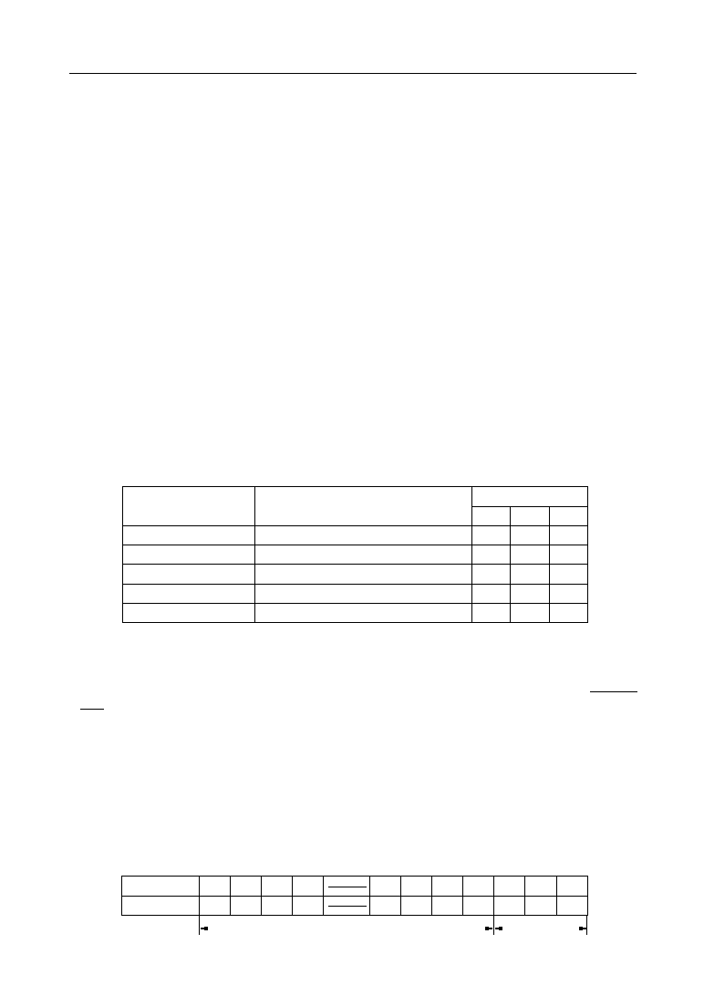
Master Mode
Master Mode is selected when M/S pin is set at High level. The master mode operation is as
follows:
∑ The input levels of DIM IN, SYNC IN1 and SYNC IN2 are ignored, and these pins should be
connected to L-GND or V
DD
.
∑ The pulse width of GRID1 to 3 and SEG1 to 32 are controlled by the internal digital dimming
circuit.
∑ The segment Latch1 to 3 corresponding to GRID1 to 3 are selected by the internal timing
generator.
° Semiconductor
MSM9210
14/20
FEDL9210-04
SYNC IN 1
SYNC IN 2
Segment Latch
GRID
0
0
No
No
1
0
Latch1
GRID1
0
1
Latch2
GRID2
1
1
Latch3
GRID3
DIM IN
SEG1 to 32
0
Low
1
High
Slave Mode
Slave Mode is selected when M/S pin is set at Low level. The slave mode operation is as follows:
∑ The internal dimming circuit is ignored.
∑ The pulse width of SEG1 to 32 are controlled by the pulse width of DIM IN signal.
∑ The segment Latch1 to 3 corresponding to GRID1 to 3 are selected by SYNC IN1 and SYNC IN2
signals.
∑ The output levels of GRID1 to 3 are set at High level. The output levels of DIM OUT, SYNC
OUT1 and SYNC OUT2 are set at Low level.
[Correspondence between SYNC IN1, 2 and Segment Latch1 to 3] [Correspondence between DIM IN and SEG1 to 32]
Note: Low: Lights OFF
High: Lights ON
° Semiconductor
MSM9210
15/20
FEDL9210-04
APPLICATION CIRCUITS
1. Circuit for the duplex VFD tube with 128 segments (2 Grid
•
64 Anode)
MSM9210
(MASTER)
V
DISP
V
DD
D-GND
L-GND
OSC 0
OSC 1
CLOCK
DATA IN
CS
DIM IN
SYNC IN 1
SYNC IN 2
M/S
DUP/TRI
DIM OUT
SYNC OUT 1
SYNC OUT 2
GRID2
GRID1
GRID3
SEG1
SEG32
MSM9210
(SLAVE)
V
DISP
V
DD
D-GND
L-GND
OSC 0
OSC 1
CLOCK
DATA IN
CS
DIM IN
SYNC IN 1
SYNC IN 2
DIM OUT
SYNC OUT 1
SYNC OUT 2
GRID2
GRID1
GRID3
SEG1
SEG32
V
DD
Duplex VF Tube
S62 S63 S64
S1 S2 S3
G1
G2
Microcontroller
V
DISP
V
DD
M/S
GND
DUP/TRI
V
DD
Ef
GND
GND
GND
R
C
GND
R
C
° Semiconductor
MSM9210
16/20
FEDL9210-04
2. Circuit for the triplex VFD tube with 192 segments (3 Grid
•
64 Anode)
MSM9210
(MASTER)
V
DISP
V
DD
D-GND
L-GND
OSC 0
OSC 1
CLOCK
DATA IN
CS
DIM IN
SYNC IN 1
SYNC IN 2
DUP/TRI
M/S
DIM OUT
SYNC OUT 1
SYNC OUT 2
GRID2
GRID1
GRID3
SEG1
SEG32
MSM9210
(SLAVE)
V
DISP
V
DD
D-GND
L-GND
OSC 0
OSC 1
CLOCK
DATA IN
CS
DIM IN
SYNC IN 1
SYNC IN 2
DUP/TRI
M/S
DIM OUT
SYNC OUT 1
SYNC OUT 2
GRID2
GRID1
GRID3
SEG1
SEG32
V
DD
Triplex VF Tube
S62 S63 S64
S1 S2 S3
G1
G2
Microcontroller
V
DISP
V
DD
GND
Ef
GND
GND
R
C
GND
GND
R
C
G3
° Semiconductor
MSM9210
17/20
FEDL9210-04
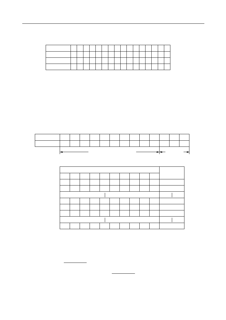
NOTES ON TURNING POWER ON/OFF
∑ Connect L-GND and D-GND externally to be an equal potential voltage.
∑ To avoid wrong operations, turn on the driver power supply after turning on the logic power
supply. Conversely, turn off the logic power supply after tuning off the driver power supply.
[Voltage]
[Time]
V
DD
V
DISP
° Semiconductor
MSM9210
18/20
FEDL9210-04
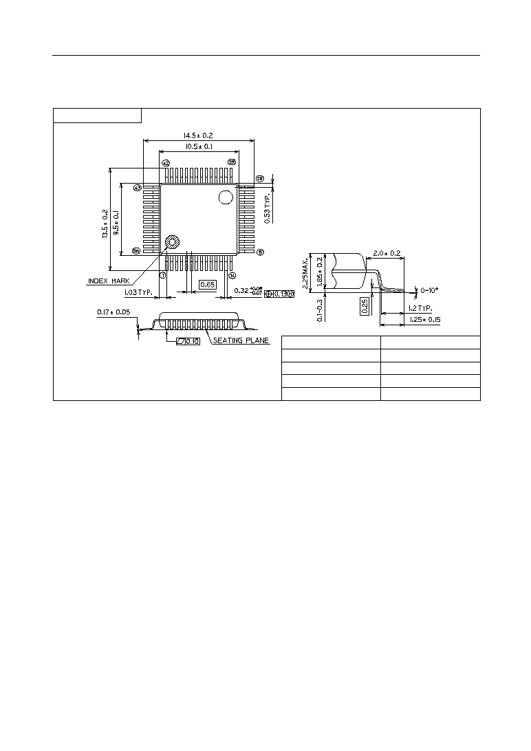
(Unit : mm)
PACKAGE DIMENSIONS
Notes for Mounting the Surface Mount Type Package
The SOP, QFP, TSOP, SOJ, QFJ (PLCC), SHP and BGA are surface mount type packages, which
are very susceptible to heat in reflow mounting and humidity absorbed in storage.
Therefore, before you perform reflow mounting, contact Oki's responsible sales person for the
product name, package name, pin number, package code and desired mounting conditions
(reflow method, temperature and times).
QFP56-P-910-0.65-2K
Mirror finish
Package material
Lead frame material
Pin treatment
Package weight (g)
Oki Electric Industry Co., Ltd.
Rev. No./Last Revised
Epoxy resin
42 alloy
Solder plating (5 mm)
0.43 TYP.
4/Nov. 28, 1996
° Semiconductor
MSM9210
19/20
FEDL9210-04
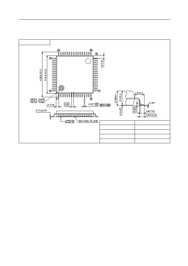
(Unit : mm)
Notes for Mounting the Surface Mount Type Package
The SOP, QFP, TSOP, SOJ, QFJ (PLCC), SHP and BGA are surface mount type packages, which
are very susceptible to heat in reflow mounting and humidity absorbed in storage.
Therefore, before you perform reflow mounting, contact Oki's responsible sales person for the
product name, package name, pin number, package code and desired mounting conditions
(reflow method, temperature and times).
QFP64-P-1414-0.80-BK
Package material
Lead frame material
Pin treatment
Package weight (g)
Oki Electric Industry Co., Ltd.
Rev. No./Last Revised
Epoxy resin
42 alloy
Solder plating (5 mm)
0.87 TYP.
5/Sept. 21, 1999

° Semiconductor
MSM9210
20/20
FEDL9210-04
NOTICE
1.
The information contained herein can change without notice owing to product and/or
technical improvements. Before using the product, please make sure that the information
being referred to is up-to-date.
2.
The outline of action and examples for application circuits described herein have been
chosen as an explanation for the standard action and performance of the product. When
planning to use the product, please ensure that the external conditions are reflected in the
actual circuit, assembly, and program designs.
3.
When designing your product, please use our product below the specified maximum
ratings and within the specified operating ranges including, but not limited to, operating
voltage, power dissipation, and operating temperature.
4.
Oki assumes no responsibility or liability whatsoever for any failure or unusual or
unexpected operation resulting from misuse, neglect, improper installation, repair, alteration
or accident, improper handling, or unusual physical or electrical stress including, but not
limited to, exposure to parameters beyond the specified maximum ratings or operation
outside the specified operating range.
5.
Neither indemnity against nor license of a third party's industrial and intellectual property
right, etc. is granted by us in connection with the use of the product and/or the information
and drawings contained herein. No responsibility is assumed by us for any infringement
of a third party's right which may result from the use thereof.
6.
The products listed in this document are intended for use in general electronics equipment
for commercial applications (e.g., office automation, communication equipment,
measurement equipment, consumer electronics, etc.). These products are not authorized
for use in any system or application that requires special or enhanced quality and reliability
characteristics nor in any system or application where the failure of such system or
application may result in the loss or damage of property, or death or injury to humans.
Such applications include, but are not limited to, traffic and automotive equipment, safety
devices, aerospace equipment, nuclear power control, medical equipment, and life-support
systems.
7.
Certain products in this document may need government approval before they can be
exported to particular countries. The purchaser assumes the responsibility of determining
the legality of export of these products and will take appropriate and necessary steps at their
own expense for these.
8.
No part of the contents contained herein may be reprinted or reproduced without our prior
permission.
9.
MS-DOS is a registered trademark of Microsoft Corporation.
Copyright 2000 Oki Electric Industry Co., Ltd.
Printed in Japan