 | –≠–ª–µ–∫—Ç—Ä–æ–Ω–Ω—ã–π –∫–æ–º–ø–æ–Ω–µ–Ω—Ç: MSM92RB09 | –°–∫–∞—á–∞—Ç—å:  PDF PDF  ZIP ZIP |
MSM30R/32R/92R
0.5µm Sea Of Gates and
Customer Structured Arrays
August 2002
O
K
I
A
S
I
C
P
R
O
D
U
C
T
S
D
ATA
S
HEET

0
Oki Semiconductor
I
I
≠≠≠≠≠≠≠≠≠≠≠≠≠≠≠≠≠≠≠≠≠≠≠≠≠≠≠≠≠≠≠≠≠≠≠≠≠≠≠≠≠≠≠≠≠≠≠≠≠≠≠≠≠≠≠≠≠≠≠≠≠≠≠≠≠≠≠≠≠≠≠≠≠≠≠≠≠≠≠≠≠≠≠≠≠≠≠≠≠≠≠
CONTENTS
Description ................................................................................................................................................................1
Features ....................................................................................................................................................................1
MSM30R/32R/92R Family Listing .......................................................................................................................2
Array Architecture ...................................................................................................................................................3
MSM92R000 CSA Layout Methodology ........................................................................................................3
Electrical Characteristics .........................................................................................................................................5
Macro Library .........................................................................................................................................................10
Macrocells for Driving Clock Trees ..............................................................................................................11
Oki Advanced Design Center Cad Tools ..........................................................................................................1 2
Design Process .................................................................................................................................................13
Automatic Test Pattern Generation ..............................................................................................................14
Floorplanning Design Flow ...........................................................................................................................14
IEEE JTAG Boundary Scan Support .............................................................................................................15
Package Options .....................................................................................................................................................16
1
Oki Semiconductor
MSM30R/32R/92R
Second-Generation 0.5
µ
m Sea of Gates and Customer Structured Arrays
DESCRIPTION
Oki's second-generation 0.5µm ASIC products are available in both Sea Of Gates (SOG) and Customer
Structured Array (CSA) architectures. The MSM30R Series, MSM32R Series, and MSM92R Series all offer
increased density over their first-generation counterparts, as well as 3-V I/O buffers that are 5-V tolerant.
Both the SOG-based MSM30R Series and the CSA-based MSM92R Series use a three-layer metal process
on 0.5µm drawn (0.4µm L-effective) CMOS technology. The SOG-based MSM32R Series uses the same
SOG base-array architecture as the MSM30R Series, but offers two metal layers instead of three. The
semiconductor process is adapted from Oki's production-proven 16-Mbit DRAM manufacturing process.
The second-generation 0.5µm family retains the high speed and low power of Oki's first-generation
0.5µm MSM13R/12R/98R family. The second-generation 0.5µm family also shares the same die sizes for
arrays with corresponding I/O counts, but the second-generation arrays can contain up to 60% more
gates than their first-generation counterparts. The second-generation family is optimized for 3-V core
operation, with optimized 3-V I/O buffers and 3-V I/O buffers that are 5-V tolerant, whereas the first-
generation family offers separate I/O buffers for mixed 3-V and 5-V operation. Oki's first-generation and
second-generation 0.5µm families together offer an unusually flexible mixed-voltage ASIC capability.
The 3-layer-metal MSM30R SOG Series contains 8 array bases, offering up to 448 I/O pads and over 600K
raw gates. The 2-layer metal MSM32R SOG Series contains five array bases, offering up to 320 I/O pads
and over 300K raw gates. These SOG array sizes are designed to fit the most popular Quad Flat Pack
(QFP) and Plastic Ball Grid Array (PBGA) packages. The MSM30R and MSM32R Series' SOG architec-
ture allows rapid prototyping turnaround times, additionally offering the most cost-effective solution for
pad-limited circuits (particularly the 2-layer metal MSM32R Series).
The 3-layer-metal MSM92R CSA Series contains 36 array bases, offering a wider span of gate and I/O
counts than SOG Series. Oki uses the EPOCH memory compiler from Cascade Design Automation to
generate optimized single- and dual-port RAM macrocells for CSA designs. As such, the MSM92R Series
is suited to memory-intensive ASICs and high-volume designs where fine tuning of package size pro-
duces significant cost or real-estate savings.
FEATURES
∑ 0.5
µm drawn two and three-layer metal CMOS
∑ Optimized 3.3-V core
∑ Optimized 3-V I/O and 3-V I/O that is 5-V tolerant
∑ SOG and CSA architecture availability
∑ 120-ps typical gate propagation delay (for a 2-input
4x-drive NAND gate with a fan-out of 2 and 0mm of
wire, operating at 3.3 V)
∑ Up to 1.2M raw gates and 624 pads
∑
User-configurable I/O with V
SS
, V
DD
, TTL, 3-state,
and 1 mA ~ 24 mA options
∑ Slew-rate-controlled outputs for low-radiated noise
∑ Clock tree cells with
0.5-ns clock skew, worst-case
(fan-out
9000 at 75 MHz)
∑ User-configurable single and dual-port memories
∑ Specialized macrocells, including phase-locked loop,
GTL, PECL, and PCI cells
∑ Floorplanning for front-end simulation, back-end
layout controls, and link to synthesis
∑ JTAG boundary scan and scan-path ATPG
∑ Support for popular CAE systems, including
Cadence, IKOS, Mentor Graphics, Synopsys,
Viewlogic, and Zycad
2
Oki Semiconductor
I
MSM30R/32R/92R
I
≠≠≠≠≠≠≠≠≠≠≠≠≠≠≠≠≠≠≠≠≠≠≠≠≠≠≠≠≠≠≠≠≠≠≠≠≠≠≠≠≠≠≠≠≠≠≠≠≠≠≠≠≠≠≠≠≠≠≠≠≠≠≠≠≠≠≠≠≠≠≠≠≠≠≠≠
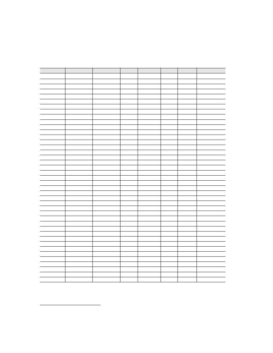
MSM30R/32R/92R FAMILY LISTING
CSA Part#
CSA Master#
SOG Part#
I/O Pads
Raw Gates
Rows
[1]
1. Row and column numbers are used to evaluate the number and size of mega macrocells that may be included into each array.
Columns
Usable Gates
[2]
2. Usable gate count is design dependent and varies based upon the number of fan-outs per net, internal busses, floor plan,
RAM/ROM blocks, etc.
MSM92RB01
B92R020X020
--
80
14,688
72
204
11,750
MSM92RB02
B92R024X024
--
96
22,784
89
256
18,227
MSM92RB03
B92R026X026
MSM30R0020
104
27,440
98
280
21,952
MSM92RB04
B92R030X030
--
120
37,720
115
328
30,176
MSM92RB05
B92R032X032
--
128
43,296
123
352
34,637
--
--
MSM32R0050
144
56,000
140
400
26,880
MSM92RB06
B92R036X036
MSM30R0050
144
56,000
140
400
42,000
MSM92RB07
B92R038X038
--
152
63,176
149
424
47,382
MSM92RB08
B92R040X040
--
160
70,336
157
448
52,752
MSM92RB09
B92R042X042
--
168
78,352
166
472
58,764
--
--
MSM32R0080
176
86,304
174
496
38,837
MSM92RB10
B92R044X044
MSM30R0080
176
86,304
174
496
60,413
MSM92RB11
B92R048X048
--
192
103,904
191
544
72,733
MSM92RB12
B92R050X050
--
200
114,400
200
572
80,080
--
--
MSM32R0120
208
123,968
208
596
49,587
MSM92RB13
B92R052X052
MSM30R0120
208
123,968
208
596
86,778
MSM92RB14
B92R056X056
--
224
144,900
225
644
101,430
MSM92RB15
B92R060X060
--
240
167,464
242
692
117,225
--
--
MSM32R0190
256
191,660
259
740
72,831
MSM92RB16
B92R064X064
MSM30R0190
256
191,660
259
740
126,496
MSM92RB17
B92R068X068
--
272
217,488
276
788
143,542
MSM92RB18
B92R072X072
--
288
244,948
293
836
161,666
MSM92RB19
B92R076X076
--
304
274,040
310
884
180,866
--
--
MSM32R0300
320
306,072
327
936
110,186
MSM92RB20
B92R080X080
MSM30R0300
320
306,072
327
936
195,886
MSM92RB21
B92R084X084
--
336
338,496
344
984
216,637
MSM92RB22
B92R088X088
--
352
372,552
361
1032
238,433
MSM92RB23
B92R092X092
--
368
408,240
378
1080
261,274
MSM92RB24
B92R096X096
MSM30R0440
384
445,560
395
1128
276,247
MSM92RB25
B92R100X100
--
400
484,512
412
1176
300,397
MSM92RB26
B92R104X104
--
416
525,096
429
1224
325,560
MSM92RB27
B92R108X108
--
432
569,096
446
1276
352,840
MSM92RB28
B92R112X112
--
448
613,012
463
1324
367,807
MSM92RB29
B92R118X118
--
472
682,644
489
1396
409,586
MSM92RB30
B92R122X122
--
488
730,664
506
1444
438,398
MSM92RB31
B92R126X126
--
504
780,316
523
1492
468,190
MSM92RB32
B92R132X132
--
528
857,072
548
1564
514,243
MSM92RB33
B92R138X138
--
552
941,360
574
1640
564,816
MSM92RB34
B92R144X144
--
576
1,025,488
599
1712
615,293
MSM92RB35
B92R150X150
--
600
1,115,000
625
1784
669,000
MSM92RB36
B92R156X156
--
624
1,206,400
650
1856
723,840
3
Oki Semiconductor
≠≠≠≠≠≠≠≠≠≠≠≠≠≠≠≠≠≠≠≠≠≠≠≠≠≠≠≠≠≠≠≠≠≠≠≠≠≠≠≠≠≠≠≠≠≠≠≠≠≠≠≠≠≠≠≠≠≠≠≠≠≠≠≠≠≠≠≠≠≠≠≠≠≠≠
I
MSM30R/32R/92R
I
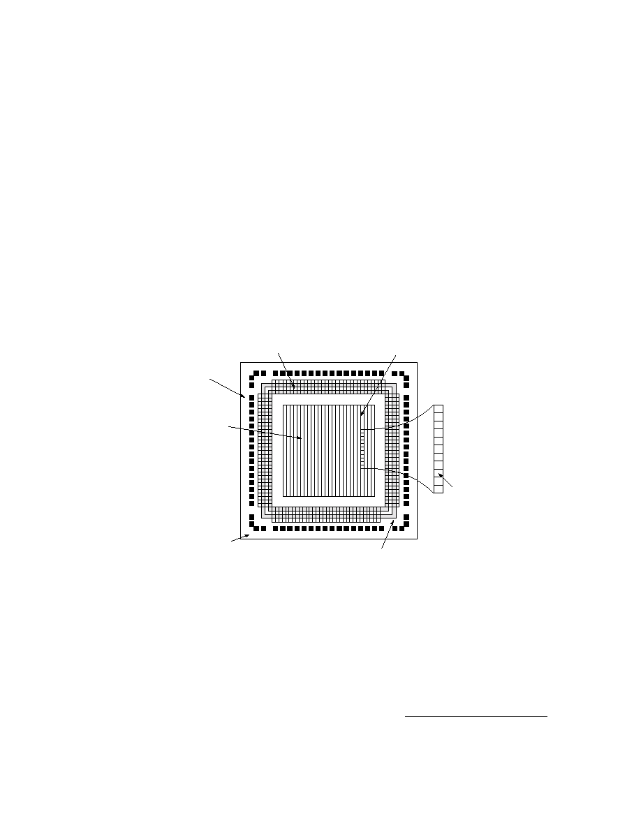
ARRAY ARCHITECTURE
The primary components of a 0.5
µ
m MSM30R/32R/92R circuit include:
∑ I/O base cells
∑ Configurable I/O pads for V
DD
, V
SS
, or I/O (optimized 3-V I/O and 3-V I/O that is 5-V tolerant)
∑ V
DD
and V
SS
pads dedicated to wafer probing
∑ Separate power bus for output buffers
∑ Separate power bus for internal core logic and input buffers
∑ Core base cells containing N-channel and P-channel pairs, arranged in column of gates
∑ Isolated gate structure for reduced input capacitance and increased routing flexibility
Each array has 24 dedicated corner pads for power and ground use during wafer probing, with four pads
per corner. The arrays also have separate power rings for the internal core functions (V
DDC
and V
SSC
)
and output drive transistors (V
DDO
and V
SSO
).
Figure 7. MSM30R0000 Array Architecture
MSM92R000 CSA Layout Methodology
The procedure to design, place, and route a CSA follows.
1. Select suitable base array frame from the available predefined sizes. To select an array size:
- Identify the macrocell functions required and the minimum array size to hold the macrocell
functions.
Core base cell
with 4 transistors
Separate power bus (V
DDO
, V
SSO
)
over I/O cell for output buffers(2nd
metal/3rd metal)
V
DD
, V
SS
pads (4) in each
corner for
wafer probing only
Configurable I/O pads
for V
DD
, V
SS
, or I/O
Separate power bus (V
DDC
, V
SSC
) for
internal core logic (2nd metal/3rd metal
I/O base cells
1,2, or 3 layer metal
interconnection in
core area